fabrication and characterization of carbon … · fabrication and characterization of carbon...
TRANSCRIPT

FABRICATION AND CHARACTERIZATION OF CARBON NANOTUBES
FOR BIOMEDICAL APPLICATIONS
by
Zhiyang Rong
A Thesis
Submitted to the Faculty
of the
WORCESTER POLYTECHNIC INSTITUTE
in partial fulfillment of the requirements for the
Degree of Master of Science
in
Mechanical Engineering
August 2008
APPROVED:
Dr. Jianyu Liang, Advisor
Dr. Cosme Furlong, Graduate committee
representative
Dr. Hong Zhou, Committee member
Dr. Richard D. Sisson, Jr., Committee
member
i
ABSTRACT
Recently, nanomaterials have been vigorously studied for the development of
biosensors. Among them, carbon nanotubes (CNTs) have stimulated enormous
interest for constructing biosensors due to their unique physical and chemical
properties such as high surface-to-volume ratio, high conductivity, high strength and
chemical inertness. Our study is to develop a general design of biosensors based on
vertically aligned CNT arrays. Glucose biosensor is selected as the model system to
verify the design of biosensors. In the preliminary design, glucose oxidase (GOx) is
attached to the walls of the porous alumina membrane by adsorption. Porous highly
ordered anodized aluminum oxide (AAO) prepared by two-step anodization are used
as templates. Deposited gold on both sides of template surfaces serve as a contact and
prevent non-specific adhesion of GOx on the surface. In order to find out optimized
thickness of gold coating, the oxidation and reduction (redox) reaction in [Fe(CN)6]3–
/[Fe(CN)6]4– system is monitored by Cyclic Voltammetry (CV). Subsequently,
enzymatic redox reaction in glucose solutions is also attempted by CV. We expect
protein layers with GOx form a conductive network. However, no obvious enzymatic
redox reaction is detected in the voltammogram. To take advantage of the attractive
properties of CNTs, the design of enzyme electrodes is modified by attaching CNT
onto the sidewalls of AAO template nanopores and then immobilizing GOx to the
sidewalls and tips of CNTs. AAO templates provided vertical, parallel, well separated
and evenly spacing nanochannels for CNT growth. Cobalt is used as a catalyst to
fabricate CNTs. As a result, multi-walled carbon nanotubes (MWCNTs) are fabricated
ii
inside the AAO templates by catalytic chemical vapor deposition (CCVD).
Characterization of AAO templates and cobalt electrochemical deposition are
employed by scanning electron microscope (SEM), and energy dispersive X-ray
spectrometry (EDS). Detailed structure and texture of CNTs are examined by
transmission electron microscope (TEM).
iii
ACKNOWLEDGMENTS
I would like to sincerely thank my advisor Dr. Jianyu Liang for being such an
incredible mentor during my graduate period. Professor Liang is a diligent person
with great energy. Her passion for work has deeply impressed me. I have also been
motivated by her keen perspective on academic research. Throughout the whole
project, she gave me many precious suggestions and has always been ready to answer
my questions. I’m very glad that I had a chance to work in her Nanomaterials and
Nanomanufacturing Laboratory for the past two years. It leaves me with a most
valuable memory in my academic life. I have learned more than I could ever image.
I would also like to thank all my colleagues at WPI. In particular, I’d like to thank
Dr. Boquan Li, who has provided me with training on the SEM and TEM. Dr. Li is an
accommodating person. Without his help, I would not be able to take any SEM or
TEM images for my thesis. Additionally, I’d like to thank all the members in our
group: Shelley Dougherty, Huanan Duan, Dawei Zhang and Ryan Blair. They are all
warmhearted people who have helped me in my research and thesis. As the eldest
graduate students in our lab, Shelley and Huanan have taught me a lot during the
experiments. Shelley has collaborated on some of my earliest work. Without her
initially getting me started, I would have taken a much longer time to get on the right
track. Huanan has always been willing to share his broad knowledge with me. Thanks
to his demonstration on the fabrication of anodized aluminum oxidase, I was able to
continue my research much further. I would also like to thank, Dawei Zhang and
Ryan, who have made their efforts in improving my thesis.
iv
Additionally, I would like to give my special thank to my family: my father
(Yixiang Rong), my mother (Pei Qi), my uncle (Yiming Rong) and my aunt (Jiaoshi
Dong). They encouraged me to attend graduate college abroad and have been
inspirational throughout my life. Without their great love and lifelong support, I
certainly would not be able to achieve what I’ve done.
Finally, I would like to thank my friends Yue Wang, Dong Lu, Xuekun Li, Hua
Li, Lei Zhang and Feng Liu. All of you have made my days at WPI very
unforgettable.
v
TABLE OF CONTENTS
ABSTRACT i
ACKNOWLEDGMENTS iii
TABLE OF CONTENTS v
LIST OF FIGURES vii
LIST OF TABLES ix
ABBREVIATIONS AND SYMBOLS xii
1. Introduction 1 1.1 Introduction to carbon nanotubes (CNTs) 1
1.1.1 Structure of CNTs 3
1.1.2 Properties and applications of CNTs 6
1.1.3 Synthesis of nanotubes growth 10
1.1.3.1 Electric arc-discharge method 10
1.1.3.2 Laser ablation method 12
1.1.3.3 Catalytic chemical vapor deposition (CCVD) 13
1.1.3.4 Comparison of different CNT growth methods 15
1.2 Introduction to biosensors 16
1.2.1 Glucose biosensors 17
1.2.2 GOx immobilization 20
1.2.3 CNT-based biosensors 22
1.3 Introduction to characterization methods 24
1.3.1 Characterization of CNTs 24
1.3.2 Electrochemical methods 25
2. Materials and methods 29 2.1 Anodized aluminum oxide (AAO) template 29
2.2 Methodology of electrode design 32
2.2.1 Preliminary electrode design 32
vi
2.2.2 CNT-based electrode design 34
3. Experimental 36 3.1 Preparation of AAO template 36
3.2 Study of gold deposition 37
3.3 Preliminary biosensor construction 38
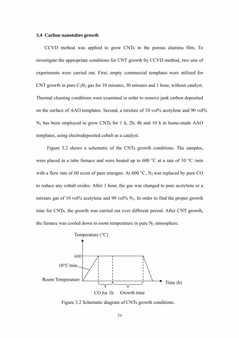
3.4 Carbon nanotubes growth 39
4. Results and discussions 41 4.1 Characterization of AAO templates 41
4.2 Study of Au coating 43
4.3 Characterization of cobalt deposition 45
4.4 Observation of CNTs 48
4.3.1 CNT growth in pure C2H2 48
4.3.2 CNT growth in C2H2 and N2 mixture gas 50
5. Conclusions 54
6. Future work 55
7. References 56
APPENDIX 62 Appendix A Demonstrated image analysis by ImageJ software 62
Appendix B Other image analysis by ImageJ 67
vii
LIST OF FIGURES
Figure 1.1 High resolution TEM images of MWCNTs, showing different diameters and diverse numbers of graphene sheets [1]. 1
Figure 1.2 Rolling of graphite sheet into a SWCNT [4]. 1
Figure 1.4 Textures of MWCNTs (a) herringbone texture and (b) bamboo texture [8]. 3
Figure 1.3 Three structures of SWCNTs: (a) armchair, (b) zigzag, (c) chiral nanotubes and (d) the structure of MWCNTs. (Adapted from [8]) 3
Figure 1.5 Construction of graphene sheet and important parameters for CNTs:
Cv
is chiral vector, T is tube axis, θ is chiral angle (Adapted from [8]). 4
Figure 1.6 Different electronic properties with respect to various chiral angles. is semi-conductive, while is metallic (Adapted from [11]). 7
Figure 1.7 Sketch of an electric arc reactor [8]. 10
Figure 1.8 Sketch of synthesizing CNTs by a laser vaporization method [8]. 12
Figure 1.9 Experimental arrangement of synthesizing carbon nanotubes from hydrocarbon gas by catalytic chemical vapor deposition (CCVD) (adapted from [8]). 13
Figure 1.10 Two mechanisms of CNT growth: (a) base-growth (b) top-growth models. 14
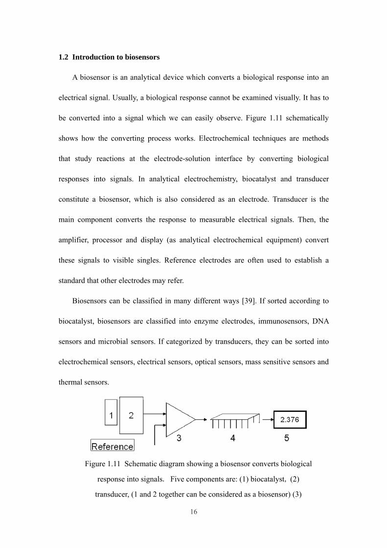
Figure 1.11 Schematic diagram showing a biosensor converts biological response into signals. Five components are: (1) biocatalyst, (2) transducer, (1 and 2 together can be considered as a biosensor) (3) amplifier, (4) processor and (5) display. 16
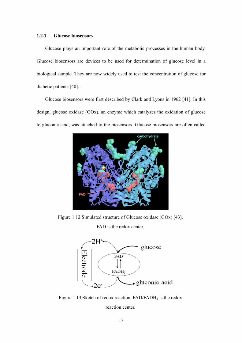
Figure 1.12 Simulated structure of Glucose oxidase (GOx) [43]. FAD is the redox center. 17
Figure 1.13 Sketch of redox reaction. FAD/FADH2 is the redox reaction center. 17
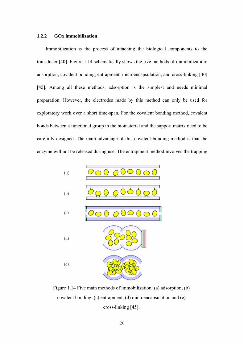
Figure 1.14 Five main methods of immobilization: (a) adsorption, (b) covalent bonding, (c) entrapment, (d) microencapsulation and (e) cross-linking [45]. 20
viii
Figure 1.15 Immobilization of GOx via the walls (a) [56] and tips (b) [55] of CNTs. 23
Figure 1.16 Triangular potential in cyclic voltammetry technique (adapted from [66]). 25
Figure 1.17 Typical cyclic voltammogram, showing one cycle of reversible redox reaction [66]. 26
Figure 2.1 Schematic diagram of the two-step anodization process. (a) first anodization; (b) pretextured Al; (c) second anodization [68]. 29
Figure 2.2 Diagram of the typical porous alumina structure when fabricated using bulk aluminum [73]. 30
Figure 2.3 Methodology of preliminary electrochemical glucose biosensor design. 32
Figure 2.4 Chemical structure of APA (a) and GA (b). 33
Figure 2.5 Methodology of CNT-based electrochemical glucose biosensor design. 34
Figure 2.6 Schematic diagrams of CNT-based electrode fabrication (a) and GOx immobilization (b). 35
Figure 3.1 Schematic diagram of preparing AAO templates with gold coating. 37
Figure 3.2 Schematic diagram of CNTs growth conditions. 39
Figure 4.1 Top-view (a) and cross-section (b) SEM images of AAO template after two-step anodization. 41
Figure 4.2 Top-view SEM image of AAO template after pore widening. 42
Figure 4.3 Cyclic voltammogram of homemade AAO template with different thickness of gold coating. 43
Figure 4.4 Top-view SEM image of empty homemade AAO template with 50nm thickness gold coating. 44
Figure 4.5 Top-view (a) and cross-section (b) SEM images of AAO template after cobalt deposition. 45
ix
Figure 4.6 Cross-section EDS spectrum of the AAO template after cobalt deposition. 45
Figure 4.7 Cross-section SEM image of the AAO template after cobalt deposition (a) and EDS spectrum line scan along the length of the nanopore from bottom to top. (b). 47
Figure 4.8 Schematic diagram of thermal cleaning. 48
Figure 4.9 Top-view SEM images of commercial AAO templates before (a) and after (b) thermal cleaning. 48
Figure 4.11 High resolution top-view SEM images of AAO templates with CNTs inside nanopores after 5h etching. 50
Figure 4.10 (a) Top-view and (b) cross-section SEM images of AAO templates after 1h CNT growth. 50
Figure 4.12 TEM images of MWCNT with an open tip (b, c) and bubble texture (a). 51
Figure 4.13 Top-view SEM images of AAO template after 2h (a), 4h (b) and 10h (c) CNT growth. 52
Figure 4.14 Top-view SEM image of homemade AAO template after thermal cleaning procedure for 2 h CNT growth. 53
Figure 4.15 Cross-section SEM image of homemade AAO template for 4 h CNT growth. 53
Fig. A1 Tool bar of ImageJ 62
Fig. A2 Set scale in ImageJ 63
Fig. A4 Threshold adjusting result figure in imageJ. 64
Fig. A3 Adjust threshold in ImageJ. 64
Fig. A5 Analyze particles dialogue window in imageJ. 65
Fig. A6 Analysis result figure in ImageJ. 66
x
Fig. B1 ImageJ analysis results image of AAO template after pore widening. 67
Fig. B2 ImageJ analysis results image of empty homemade AAO template with 50nm thickness gold coating. 68
Fig. B3 ImageJ analysis results image of top-view SEM images of AAO templates with CNTs inside nanopores after 5h etching. 68

xi
LIST OF TABLES
Table 2.1 Optimized anodization conditions for various electrolytes [70] 31
Table 4.1 SEM cross-section and EDS line scan results of electrodeposited cobalt length for 1 min 46
xii
ABBREVIATIONS AND SYMBOLS
AAO anodized aluminum oxide
AFM atomic force microscopy
APA 3-amino propylphosphonic acid
CCVD catalytic chemical vapor deposition
CNTs carbon nanotubes
CV cyclic voltammetry
DET direct electron transfer
EDS energy dispersive spectrometer
FAD flavin adenine dinucleotide
[Fe(CN)6]3– ferricyanide
[Fe(CN)6]4– ferrocyanide
GA glutaraldehyde
GOx glucose oxidase
MWCNTs multi-walled carbon nanotubes
redox oxidation and reduction
sccm standard-state cubic centimeter per minute
SCE saturated calomel electrode
SEM scanning electron microscopy
SHE standard hydrogen electrode
STM scanning tunneling microscopy
SWCNTs single-walled carbon nanotubes
xiii
TEM transmission electron microscopy
XRD X-ray diffraction
θ chiral angle
ΔE peak separation
A electrode area
C concentration
Cv
chiral vector
D diffusion coefficient
E0 standard redox potential
E1/2 polarographic half-wave potential
Ep peak potential
Ep/2 half-peak potential
n number of electrons
T tube axis
v potential scan rate
1
1. Introduction
1.1 Introduction to carbon nanotubes (CNTs)
Carbon nanotubes (CNTs) are rolled up cylinders of graphene sheets. They were
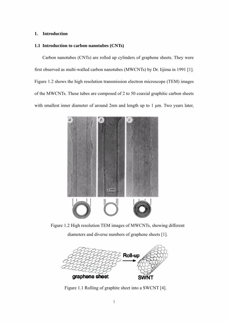
first observed as multi-walled carbon nanotubes (MWCNTs) by Dr. Iijima in 1991 [1].
Figure 1.2 shows the high resolution transmission electron microscope (TEM) images
of the MWCNTs. These tubes are composed of 2 to 50 coaxial graphitic carbon sheets
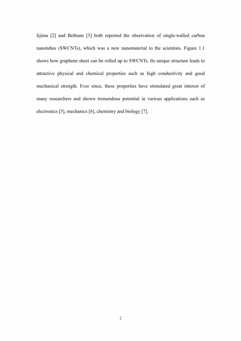
with smallest inner diameter of around 2nm and length up to 1 μm. Two years later,
Figure 1.1 Rolling of graphite sheet into a SWCNT [4].
Figure 1.2 High resolution TEM images of MWCNTs, showing different
diameters and diverse numbers of graphene sheets [1].
2
Iijima [2] and Bethune [3] both reported the observation of single-walled carbon
nanotubes (SWCNTs), which was a new nanomaterial to the scientists. Figure 1.1
shows how graphene sheet can be rolled up to SWCNTs. Its unique structure leads to
attractive physical and chemical properties such as high conductivity and good
mechanical strength. Ever since, these properties have stimulated great interest of
many researchers and shown tremendous potential in various applications such as
electronics [5], mechanics [6], chemistry and biology [7].
3
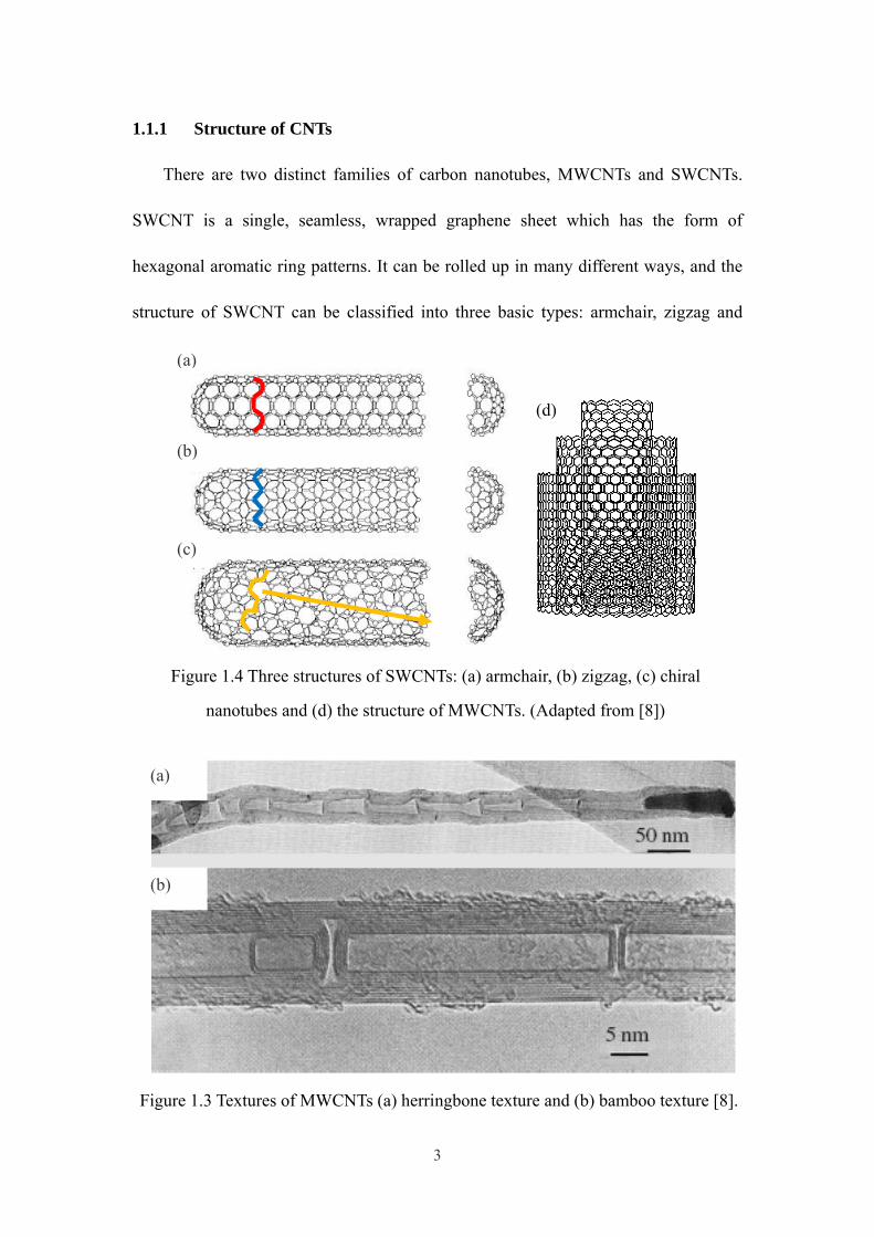
1.1.1 Structure of CNTs
There are two distinct families of carbon nanotubes, MWCNTs and SWCNTs.
SWCNT is a single, seamless, wrapped graphene sheet which has the form of
hexagonal aromatic ring patterns. It can be rolled up in many different ways, and the
structure of SWCNT can be classified into three basic types: armchair, zigzag and
(d)
(a)
(b)
(c)
Figure 1.4 Three structures of SWCNTs: (a) armchair, (b) zigzag, (c) chiral
nanotubes and (d) the structure of MWCNTs. (Adapted from [8])
(a)
(b)
Figure 1.3 Textures of MWCNTs (a) herringbone texture and (b) bamboo texture [8].
4
chiral (Figure 1.4 (a), (b), (c), respectively). MWCNTs consist of coaxial SWCNT
sheets. Figure 1.4 (d) shows the schematic structure of MWCNTs. When MWCNTs
were first discovered by Dr. Iijima, the numbers of SWCNT layers varied from 2 to
50 [1]. Theoretically, the coaxial layers are from 2 to infinite [8]. The distance
between sheets is 0.34nm [8].
MWCNTs are materials with various textures. Two common features [8] are
shown in Figure 1.3. One is the so-called herringbone texture, in which graphene
layers are at an angle with respect to the nanotube axis. The other is the so-called
“bamboo” texture, in which graphene sheets are oriented perpendicular to the
nanotubes axis.
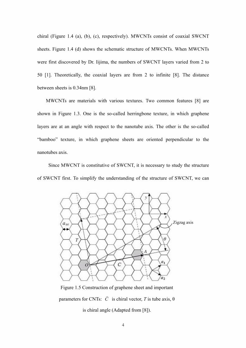
Since MWCNT is constitutive of SWCNT, it is necessary to study the structure
of SWCNT first. To simplify the understanding of the structure of SWCNT, we can
Zigzag axis
Figure 1.5 Construction of graphene sheet and important
parameters for CNTs: Cv
is chiral vector, T is tube axis, θ
is chiral angle (Adapted from [8]).
5
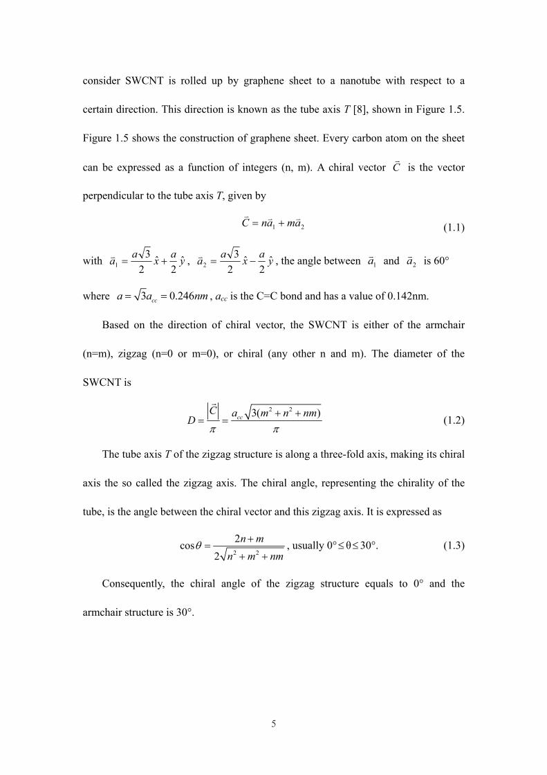
consider SWCNT is rolled up by graphene sheet to a nanotube with respect to a
certain direction. This direction is known as the tube axis T [8], shown in Figure 1.5.
Figure 1.5 shows the construction of graphene sheet. Every carbon atom on the sheet
can be expressed as a function of integers (n, m). A chiral vector Cv
is the vector
perpendicular to the tube axis T, given by
21 amanC vvv+= (1.1)
with yaxaa ˆ2
ˆ2
31 +=v , yaxaa ˆ
2ˆ
23
2 −=v , the angle between 1av and 2av is 60°
where 3 0.246cca a nm= = , acc is the C=C bond and has a value of 0.142nm.
Based on the direction of chiral vector, the SWCNT is either of the armchair
(n=m), zigzag (n=0 or m=0), or chiral (any other n and m). The diameter of the
SWCNT is
2 23( )cc
C a m n nmD
π π+ +
= =
r
(1.2)
The tube axis T of the zigzag structure is along a three-fold axis, making its chiral
axis the so called the zigzag axis. The chiral angle, representing the chirality of the
tube, is the angle between the chiral vector and this zigzag axis. It is expressed as
2 2
2cos2
n mn m nm
θ +=
+ +, usually 0°≤θ≤30°. (1.3)
Consequently, the chiral angle of the zigzag structure equals to 0° and the
armchair structure is 30°.
6
1.1.2 Properties and applications of CNTs
The unique structures of CNTs result in many attractive properties. In general, the
diameters of CNTs are in the nanometer range while the length could be at
micro-scale [9]-[11]. SWCNTs have stimulated intense interest for detailed structure
and property studies, because the original structure of SWCNTs leads to the novel
properties. For instance, SWCNTs are stable up to 750 °C in air and up to
1500-1800 °C in an inert atmosphere [8]. Properties of MWCNTs vary depending on
the structure and the texture of MWCNTs. The bond strength is quite different along
the in-plane direction and the direction perpendicular to the plane. Along the in-plane
direction, very strong covalent strength results in short bonds of 0.142nm [8].
However, in the direction perpendicular to the plane, only very weak Van der Waals
forces exist and cause loose bonds of 0.34nm [8]. Such heterogeneity can be observed
in bundles of SWNCTs and MWCNTs, but not found in individual SWCNT. Thus,
properties of CNTs may change significantly depending on whether MWCNTs or
SWCNTs are considered.
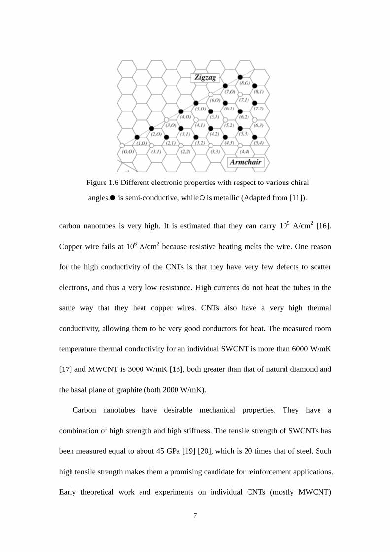
SWCNTs are unique nanostructures with unusual electronic properties, because
of the one–dimensional quantum effect. Figure 1.6 shows the early prediction that
CNTs could be either semi-conducting or metallic depending on their diameter and
the chirality of the constituent graphene tubules [12] [13]. For example, the zigzag
structure has semi-conductor or quasi-metallic properties whereas the armchair
structure behaves as a metallic material. This prediction of CNTs properties was later
confirmed experimentally [14] [15]. In the metallic state, the conductivity of the
7
carbon nanotubes is very high. It is estimated that they can carry 109 A/cm2 [16].
Copper wire fails at 106 A/cm2 because resistive heating melts the wire. One reason
for the high conductivity of the CNTs is that they have very few defects to scatter
electrons, and thus a very low resistance. High currents do not heat the tubes in the
same way that they heat copper wires. CNTs also have a very high thermal
conductivity, allowing them to be very good conductors for heat. The measured room
temperature thermal conductivity for an individual SWCNT is more than 6000 W/mK
[17] and MWCNT is 3000 W/mK [18], both greater than that of natural diamond and
the basal plane of graphite (both 2000 W/mK).
Carbon nanotubes have desirable mechanical properties. They have a
combination of high strength and high stiffness. The tensile strength of SWCNTs has
been measured equal to about 45 GPa [19] [20], which is 20 times that of steel. Such
high tensile strength makes them a promising candidate for reinforcement applications.
Early theoretical work and experiments on individual CNTs (mostly MWCNT)
Figure 1.6 Different electronic properties with respect to various chiral
angles. is semi-conductive, while is metallic (Adapted from [11]).
8
confirmed that they were one of the stiffest structures. The bending modulus of
defective MWCNTs was measured to be 2-30 GPa [21]-[23]. They buckle like straws
but do not break, and can theoretically be straightened back without any damage.
Most materials fracture on bending because of the presence of defects such as
dislocations or grain boundaries. However, this does not occur to CNTs, mainly
because they have so few defects in the structure of their walls. Another reason why
they do not fracture is that as they are bent severely, the almost hexagonal carbon
rings in the walls change in structure but do not break, which can be explained by the
rehybridization of their sp2 bonds [16].
CNTs have a high surface-to-volume ratio, high conductivity and are chemically
inert. These properties make CNTs an attractive candidate for constructing biosensors.
Large surface-to-volume ratio offers large accessible surface. High conductivity offers
a good opportunity for direct electron transfer (DET). Their chemical inertness avoids
unnecessary noise introduced to the system. On the other hand, CNTs are able to be
functionalized to connect to biomolecules. As the reactivity of graphite is known to
occur mainly through edges, perfect SWCNTs have almost no chemically active
dangling bonds. The chemical reactivity of SWCNTs comes mainly from the caps,
where pentagons exist [16]. CNTs with defects or open ends have intrinsically higher
reactivity, due to the occurrence of accessible edges at the nanotube surfaces.
The unique properties of CNTs make them promising materials in
many inorganic applications such as battery electrodes [24], mechanical
reinforcement [25] [26]and nanoprobes [27]. Meanwhile, CNTs show great potential

9
in biomedical applications such as drug delivery [28] and biosensors [29] [30].
10
1.1.3 Synthesis of nanotubes growth
1.1.3.1 Electric arc-discharge method
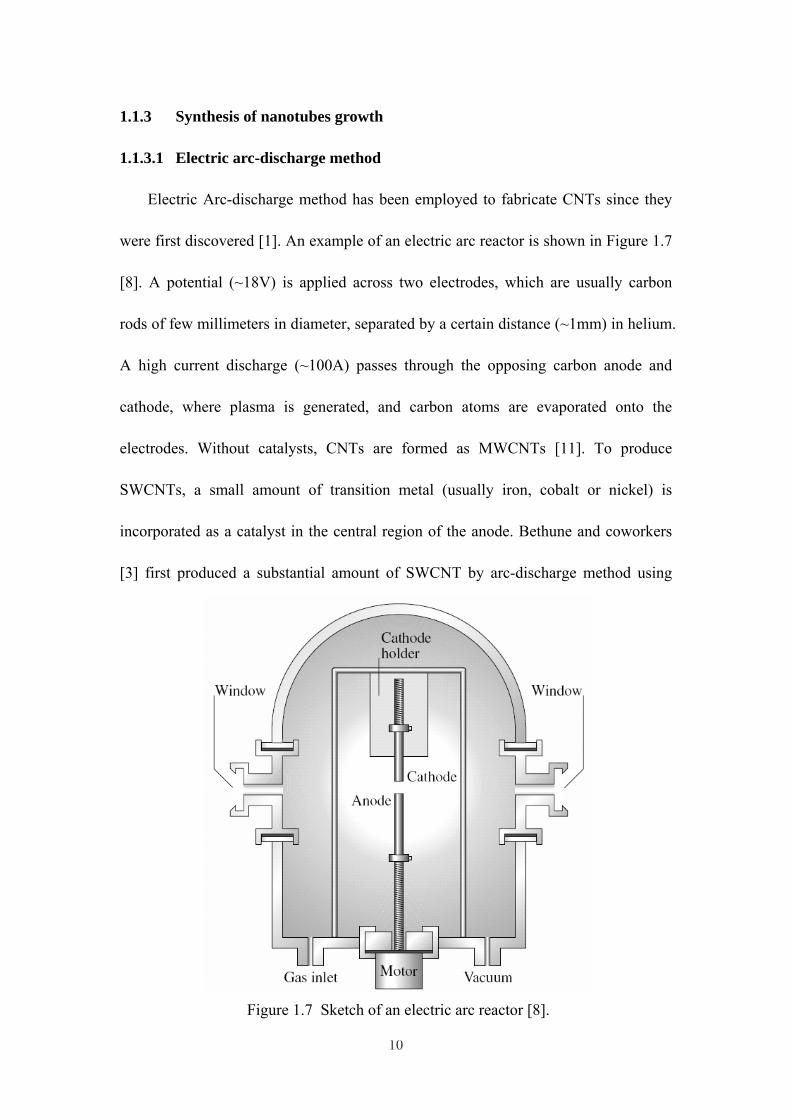
Electric Arc-discharge method has been employed to fabricate CNTs since they
were first discovered [1]. An example of an electric arc reactor is shown in Figure 1.7
[8]. A potential (~18V) is applied across two electrodes, which are usually carbon
rods of few millimeters in diameter, separated by a certain distance (~1mm) in helium.
A high current discharge (~100A) passes through the opposing carbon anode and
cathode, where plasma is generated, and carbon atoms are evaporated onto the
electrodes. Without catalysts, CNTs are formed as MWCNTs [11]. To produce
SWCNTs, a small amount of transition metal (usually iron, cobalt or nickel) is
incorporated as a catalyst in the central region of the anode. Bethune and coworkers
[3] first produced a substantial amount of SWCNT by arc-discharge method using
Figure 1.7 Sketch of an electric arc reactor [8].

11
cobalt as the catalyst. Currently, arc-discharge is the prevailing method to synthesis
high quality SWCNTs and MWCNTs.

1.1.
evap
the
A w
lase
gas,
onto
5-20
this
also
.3.2 Laser
Figure 1.8
poration me
catalyst is p
water-cooled
er beam is i
, such as a
o the colder
0nm in diam
method [31
o been synth
Figure 1.8
ablation m
8 illustrates
ethod [8]. A
placed in a f
d copper co
incident on
rgon, then
r copper col
meter and te
1]. In additi
hesized by t
8 Sketch of
method
an examp
A quartz tub
furnace and
ollector is p
the target,
sweeps the
llector wher
ens to hundr
ion to the ar
this method
f synthesizin
12
ple of the a
be containin
d maintained
partially con
evaporating
e carbon at
re they con
reds of micr
rc-discharge
[33].
ng CNTs by
apparatus fo
ng inert gas
d at a tempe
ntained in th
g carbon fr
oms from t
dense into n
rometers in
e method, h
y a laser vap
or making
and a grap
erature at 12
he tube. An
om the grap
the high-tem
nanotubes.
length hav
high-quality
porization m
CNTs by l
phite target
200°C [31]
n intense pu
phite. The i
mperature z
MWCNTs
e been mad
y SWCNTs h
method [8].
laser
with
[32].
ulsed
inert
zone
with
de by
have
13
1.1.3.3 Catalytic chemical vapor deposition (CCVD)
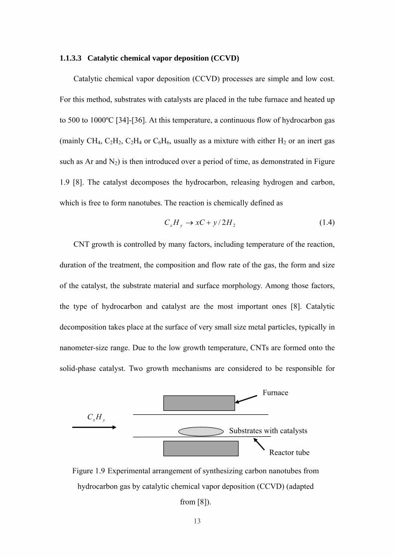
Catalytic chemical vapor deposition (CCVD) processes are simple and low cost.
For this method, substrates with catalysts are placed in the tube furnace and heated up
to 500 to 1000ºC [34]-[36]. At this temperature, a continuous flow of hydrocarbon gas
(mainly CH4, C2H2, C2H4 or C6H6, usually as a mixture with either H2 or an inert gas
such as Ar and N2) is then introduced over a period of time, as demonstrated in Figure
1.9 [8]. The catalyst decomposes the hydrocarbon, releasing hydrogen and carbon,
which is free to form nanotubes. The reaction is chemically defined as
22/ HyxCHC yx +→ (1.4)
CNT growth is controlled by many factors, including temperature of the reaction,
duration of the treatment, the composition and flow rate of the gas, the form and size
of the catalyst, the substrate material and surface morphology. Among those factors,
the type of hydrocarbon and catalyst are the most important ones [8]. Catalytic
decomposition takes place at the surface of very small size metal particles, typically in
nanometer-size range. Due to the low growth temperature, CNTs are formed onto the
solid-phase catalyst. Two growth mechanisms are considered to be responsible for
Substrates with catalysts yx HC
Furnace
Reactor tube
Figure 1.9 Experimental arrangement of synthesizing carbon nanotubes from
hydrocarbon gas by catalytic chemical vapor deposition (CCVD) (adapted
from [8]).
14
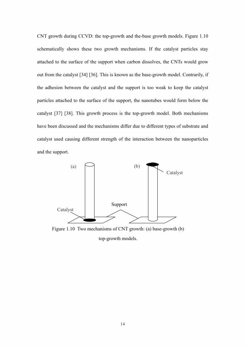
CNT growth during CCVD: the top-growth and the-base growth models. Figure 1.10
schematically shows these two growth mechanisms. If the catalyst particles stay
attached to the surface of the support when carbon dissolves, the CNTs would grow
out from the catalyst [34] [36]. This is known as the base-growth model. Contrarily, if
the adhesion between the catalyst and the support is too weak to keep the catalyst
particles attached to the surface of the support, the nanotubes would form below the
catalyst [37] [38]. This growth process is the top-growth model. Both mechanisms
have been discussed and the mechanisms differ due to different types of substrate and
catalyst used causing different strength of the interaction between the nanoparticles
and the support.
Support Catalyst
(a) (b)Catalyst
Figure 1.10 Two mechanisms of CNT growth: (a) base-growth (b)
top-growth models.
15
1.1.3.4 Comparison of different CNT growth methods
The advantages of the electric arc-discharge technique lie in the fact that very
uniform and almost defect-free nanotubes can be formed during the growing process.
The major drawback of this technique is that it is not efficient for large scale
production. Both electric arc-discharge and laser ablation techniques are well
developed to understand the mechanism of nanotube nucleation and growth. Other
disadvantages of these two techniques are the high cost and difficulty to obtain
individually separated CNTs. For example, high temperature is required for the CNT
growth and undesired tangled-shape CNTs are commonly formed. Though
arc-discharge and the laser ablation methods are generally considered not as
competitive as the CCVD method in the long term for low-cost production, they are
methods currently used to prepare CNTs for commercial products [8]. The CCVD
method is considered to be the most favorable method for mass production. Besides
its economic advantage, it is the only method of the three that can produce MWCNTs
with open end. CCVD technique creates defects, providing lots of C dangling bonds.
These dangling bonds are desirable for immobilization of biomolecules.
16
1.2 Introduction to biosensors
A biosensor is an analytical device which converts a biological response into an
electrical signal. Usually, a biological response cannot be examined visually. It has to
be converted into a signal which we can easily observe. Figure 1.11 schematically
shows how the converting process works. Electrochemical techniques are methods
that study reactions at the electrode-solution interface by converting biological
responses into signals. In analytical electrochemistry, biocatalyst and transducer
constitute a biosensor, which is also considered as an electrode. Transducer is the
main component converts the response to measurable electrical signals. Then, the
amplifier, processor and display (as analytical electrochemical equipment) convert
these signals to visible singles. Reference electrodes are often used to establish a
standard that other electrodes may refer.
Biosensors can be classified in many different ways [39]. If sorted according to
biocatalyst, biosensors are classified into enzyme electrodes, immunosensors, DNA
sensors and microbial sensors. If categorized by transducers, they can be sorted into
electrochemical sensors, electrical sensors, optical sensors, mass sensitive sensors and
thermal sensors.
Figure 1.11 Schematic diagram showing a biosensor converts biological
response into signals. Five components are: (1) biocatalyst, (2)
transducer, (1 and 2 together can be considered as a biosensor) (3)
17
1.2.1 Glucose biosensors
Glucose plays an important role of the metabolic processes in the human body.
Glucose biosensors are devices to be used for determination of glucose level in a
biological sample. They are now widely used to test the concentration of glucose for
diabetic patients [40].
Glucose biosensors were first described by Clark and Lyons in 1962 [41]. In this
design, glucose oxidase (GOx), an enzyme which catalyzes the oxidation of glucose
to gluconic acid, was attached to the biosensors. Glucose biosensors are often called
Figure 1.12 Simulated structure of Glucose oxidase (GOx) [43].
FAD is the redox center.
Figure 1.13 Sketch of redox reaction. FAD/FADH2 is the redox
reaction center.
18
enzyme electrodes and have been developed for five decades [42]. One persisting
challenge we face today is the establishment of efficient DET between GOx and the
electrode surface. Figure 1.13 shows a detailed stimulated structure of GOx molecule
[43]. Flavin adenine dinucleotide (FAD, red part in Figure 1.13) is part of GOx
structure, where redox (short form of oxidation-reduction) reaction takes place. This
FAD/FADH2 redox center is insulated deep inside the protein shell [44]. Thus, the
reactive enzyme site is a distance away from the electrode surfaces, as illustrated in
Figure 1.12. Then, the main concern for constructing biosensors becomes to establish
an efficient DET between the FAD center and the electrode surface.
The early glucose biosensors employed the reduction of glucose by oxygen:
glucose + O2 GOx⎯⎯⎯→ gluconic acid + hydrogen peroxide (1.5)
H2O2 → O2 + 2H+ +2e- (1.6)
One limitation of this method is that errors occur because of the oxygen deficit.
The concentration of oxygen is lower than that of glucose by approximately an order
of magnitude [42]. To overcome this disadvantage, mediators are used to transfer
electrons by the following scheme:
glucose + GOx (FAD) → gluconic acid + GOx (FADH2) (1.7)
GOx (FADH2) + 2M(ox) → GOx (FAD) + 2M(red)+ + 2e- (1.8)
2M(red) → 2M(ox) + 2e- (1.9)
where M(ox) and M(red) are the oxidized and reduced forms of the mediator. The
electrochemical measurements become basically independent of oxygen by using
mediators. One commonly used mediator today is ferrocene or ferricyanide [42].

19
However, mediator modified electrodes still have limitations due to the leaching
problems. Thus a more efficient electron transfer method is needed to overcome this
shortcoming.
20
1.2.2 GOx immobilization
Immobilization is the process of attaching the biological components to the
transducer [40]. Figure 1.14 schematically shows the five methods of immobilization:
adsorption, covalent bonding, entrapment, microencapsulation, and cross-linking [40]
[45]. Among all these methods, adsorption is the simplest and needs minimal
preparation. However, the electrodes made by this method can only be used for
exploratory work over a short time-span. For the covalent bonding method, covalent
bonds between a functional group in the biomaterial and the support matrix need to be
carefully designed. The main advantage of this covalent bonding method is that the
enzyme will not be released during use. The entrapment method involves the trapping
(a) (b) (c) (d) (e)
Figure 1.14 Five main methods of immobilization: (a) adsorption, (b)
covalent bonding, (c) entrapment, (d) microencapsulation and (e)
cross-linking [45].
21
of the biomaterial in a polymeric gel, which is prepared in a solution containing the
biomaterials. Unfortunately, this can cause large barriers, inhibiting the diffusion of
substrate and slowing the reaction. Enzyme activity also decreases due to pores in the
gel. Microencapsulation is quite adaptable and does not interfere with the reliability of
the enzyme. Enabling close contact between the biomaterial and the transducer, the
biomaterial is held in place behind a membrane. This method also limits
contamination and biodegradation. The cross-linking method bonds the biomaterial to
solid supports chemically or to another supporting material such as a gel. Again,
diffusion limitation and damages to the biomaterial exist.
In practice, modified electrodes with polymer coatings that facilitate the
immobilization of the biocomponents through incorporating multiple immobilization
methods are quite common for electrochemical biosensors.
Since GOx serves as the catalyst in the glucose electrolyte, GOx immobilization
on the electrodes is essential for the construction of glucose biosensors. As described
in section 1.2.1, the redox center of GOx is insulated deep inside the protein shell, so
an efficient way to establish the connections between the redox center and the
electrode surfaces is highly needed. Among all methods of immobilization, covalent
bond is the most desirable one. Functionalized CNTs offer a connection between the
FAD redox center and electrode surface by carefully designed covalent bond. Details
are discussed in the following section.
22
1.2.3 CNT-based biosensors
The main advantage of CNTs is their large accessible surface areas due to a high
surface-to-volume ratio. This offers possibility of constructing biosensors with high
sensitivity. CNT-based electrochemical glucose biosensors have improved the
performance of enzyme electrodes dramatically with high sensitivity, fast response
and good reversibility [46]-[54].
Functionalized CNTs have been studied to properly immobilize GOx [53]. There
are two ways to functionalize CNTs. One approach is to first chemically oxidize the
tips or structural defects of the CNTs and then couple them with other molecules via
carboxylic, carbonyl and/or hydroxyl groups located at the nanotube tips or its defects.
The other method is to directly add the molecules to the graphitic-like surface of the
CNTs. For both method, covalent functionalization is of the majority and is associated
with the rehybridization of sp2 bond [8]. Noncovalent functionalization is also
possible and has been achieved by wrapping the nanotubes in a polymer [8].
The most commonly used CNT-based glucose biosensors are CNT-coated
electrodes [51] . One disadvantage of these CNT-coated biosensors is the insolubility
of CNTs in most solvents. The insolubility of CNTs prohibits the electron transfer due
to the limited accessible surface. To overcome this shortcoming, Nafion was utilized
to dissolve CNTs [46].
Another advantage is that CNTs provide a direct connection between the FAD
redox center of GOx and the electrodes. Glucose biosensors based on vertically
aligned CNTs have recently received great attention [47] [55]-[57]. Figure 1.15 shows
23
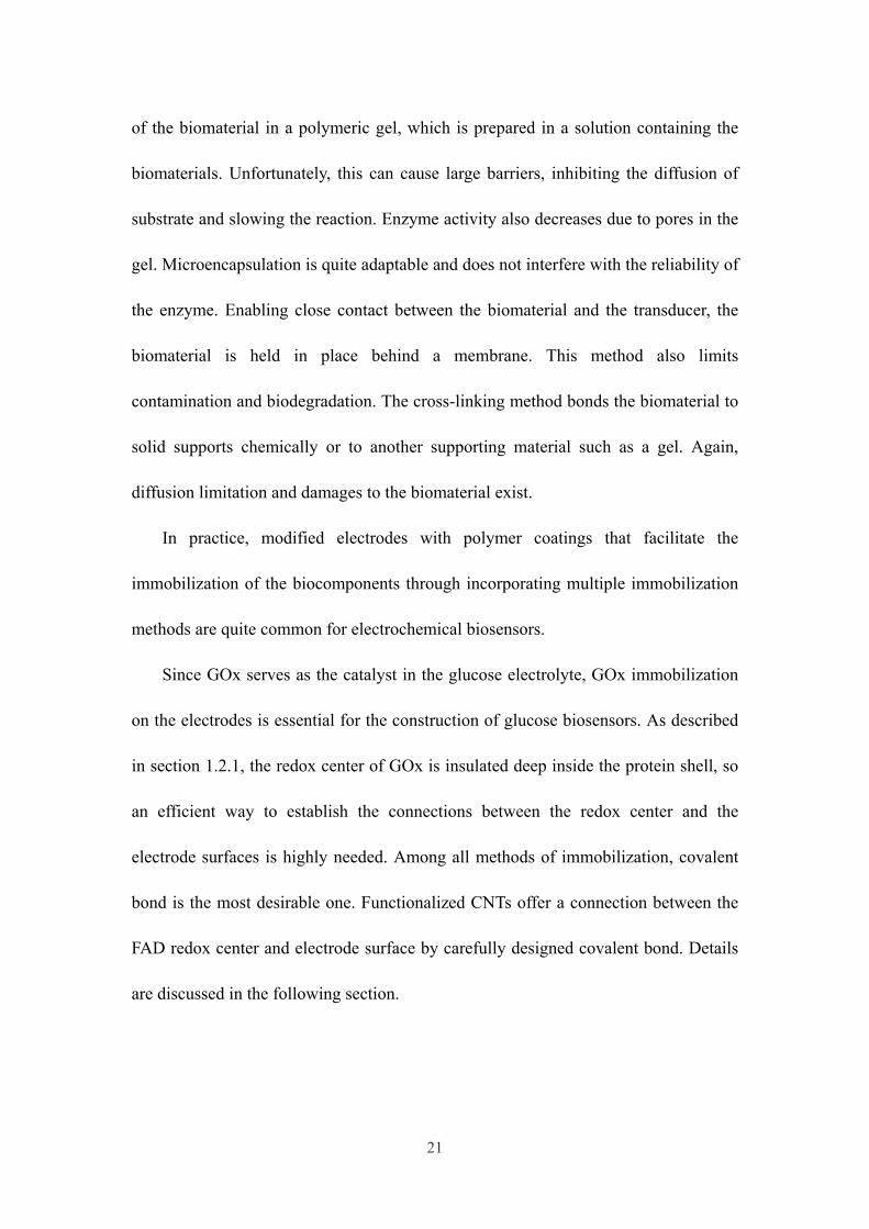
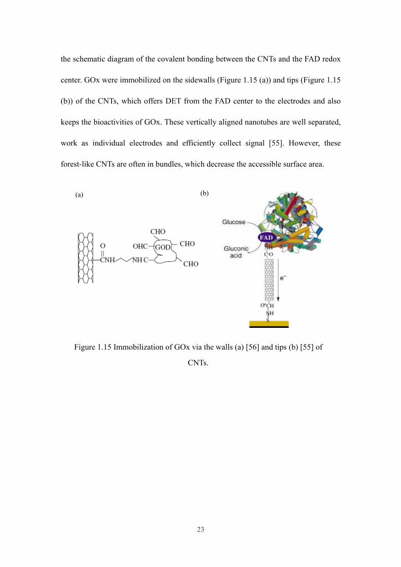
the schematic diagram of the covalent bonding between the CNTs and the FAD redox
center. GOx were immobilized on the sidewalls (Figure 1.15 (a)) and tips (Figure 1.15
(b)) of the CNTs, which offers DET from the FAD center to the electrodes and also
keeps the bioactivities of GOx. These vertically aligned nanotubes are well separated,
work as individual electrodes and efficiently collect signal [55]. However, these
forest-like CNTs are often in bundles, which decrease the accessible surface area.
Figure 1.15 Immobilization of GOx via the walls (a) [56] and tips (b) [55] of
CNTs.
(a) (b)

24
1.3 Introduction to characterization methods
1.3.1 Characterization of CNTs
To understand properties of CNTs, it is quite necessary to characterize their
structure at an atomic level. Various analytic methods have been employed to
investigate the structure of nanomaterials. For instance, scanning electron microscope
(SEM) and transmission electron microscopy (TEM) are very useful tools for imaging
and structure analysis [58] [59]. Among all electron beam instruments, SEM is the
most commonly used to obtain nanoscale information from various nanomaterials.
High-quality images are obtained with an image resolution of 0.5 nm. TEM
determines the atomic structure of interfaces and defects with high position accuracy.
The resolution of TEM reaches as high as 0.1nm. Another advantage of electron
microscope is that it offers the accessibility of associated spectroscopy and diffraction.
For example, SEM and TEM provide quantitative analysis and chemical composition
determination when combined with energy dispersive X-ray spectrometry (EDS).
To study the structure of CNTs, the most commonly used to explore the overall
structure of CNTs is TEM, which have been used ever since CNTs were discovered [1]
[2]. There are other methods that have been used to study the structure of CNTs such
as scanning tunneling microscopy (STM) [60] [61], Raman spectroscopy [62]-[64],
atomic force microscopy (AFM) [9] and X-ray Diffraction (XRD) [10].
25
1.3.2 Electrochemical methods
Among all electrochemical methods, cyclic voltammetry is the most widely used
technique for acquiring quantitative information about oxidation and reduction (redox)
reactions [65] [66]. Cyclic voltammetry studies redox properties of chemicals and
interfacial structures. It has the ability to rapidly provide considerable information on
the thermodynamics of redox processes and the kinetics of heterogeneous electron
transfer reactions and on coupled chemical reactions or adsorption processes. In an
electroananlytical study, cyclic voltammetry is often the first experiment performed.
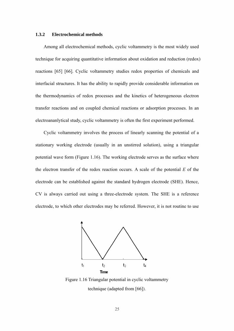
Cyclic voltammetry involves the process of linearly scanning the potential of a
stationary working electrode (usually in an unstirred solution), using a triangular
potential wave form (Figure 1.16). The working electrode serves as the surface where
the electron transfer of the redox reaction occurs. A scale of the potential E of the
electrode can be established against the standard hydrogen electrode (SHE). Hence,
CV is always carried out using a three-electrode system. The SHE is a reference
electrode, to which other electrodes may be referred. However, it is not routine to use
Figure 1.16 Triangular potential in cyclic voltammetry
technique (adapted from [66]).
26
SHE as a reference electrode because it is explosive. Other secondary reference
electrodes are used in practice. They give reproducible electrode potentials and have
low coefficients of variation with temperature. The silver-silver chloride (Ag/AgCl)
electrode and the saturated calomel electrode (SCE) are commonly used ones. The
electrodes have potentials of +0.22V and +0.24V relative to SHE, respectively. A
counter electrode, also known as an auxiliary electrode is, as well, needed in the
electrochemical system.
Single or multiple cycles can be employed to extract information about the
electrochemical process. During the potential sweep, the current resulting from the
applied potential is measured. The current and potential are then both plotted on a
diagram called a cyclic voltammogram. This diagram is a complicated,
time-dependent function of a large number of physical and chemical parameters.
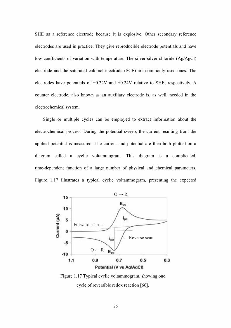
Figure 1.17 illustrates a typical cyclic voltammogram, presenting the expected
O → R
O ← R
Forward scan →
← Reverse scan
Figure 1.17 Typical cyclic voltammogram, showing one
cycle of reversible redox reaction [66].
27
response of a reversible redox couple during a single potential cycle. The reversible
redox reaction is states as:
O + ne- ⎯→← R
where O is the oxidized form, R is the reduced form.
The potential increases or decreases linearly as a function of time. When the
potential approaches a certain value E0 during the forward scan, the current begins to
increase dramatically, where the reduction process starts. The potential is then
reversed at the region that is at least 90/n mV beyond the peak. During the reverse
scan, reduced production, generated in the forward half-cycle, is reoxidized back to
the oxidized form.
The peak current for a reversible couple (25°C) is given by the Randles-Sevcik
equation
2/12/12/35 )1069.2( vACDnip ×= (1.10)
where n is the number of electrons, A the electrode area (in cm2), C the concentration
(in mol/cm3), D the diffusion coefficient (in cm2/s), and v the potential scan rate (in
V/s).
The reverse-to-forward peak current ratio, ipr/ipf, is 1 for a simple reversible
couple. The potential at which the peak occurs, Ep, is related to the standard redox
potential E0, expressed as:
2
0 pcpa EEE
+= (1.11)
The separation between the peak potentials (for a reversible couple) is given by
28
0.059p pc paE E E V
nΔ = − = (1.12)
It is possible to relate the half-peak potential Ep/2, where the current is half of the
peak current, to the polarographic half-wave potential, E1/2:
/2 1/20.056
pE E Vn
= ± (1.13)
One of the most common redox reactions used to illustrate a reversible cyclic
voltammetric response is the redox between the ferricyanide ion and ferrocyanide:
−−− ⎯→←+ 46
36 ])([])([ CNFeeCNFe (1.14)
If the electrode process is irreversible, the peaks will be reduced in size and
widely separated. However, the average of the two peak potentials is still E0. The peak
current, given by
5 1/2 1/2 1/2(2.69 10 ) ( )p ai n n ACD vα= × (1.15)
is still proportional to the bulk concentration, but will be lower in amplitude.
For a quasi-reversible system, the current is controlled by both the charge transfer
and mass transport. The voltammogram of a quasi-reversible system exhibits a greater
separation in peak potentials compared to a reversible system, but less than an
irreversible system.

29
2. Materials and methods
2.1 Anodized aluminum oxide (AAO) template
Lithography is a conventional technique used to develop controllable pattern of
small size. However, it has both technical and economical limitations such as low
throughput, long exposure time, small field size and high cost of equipment for large
scale integrated fabrication. The template-assisted technique offers a platform that
could produce large amounts of nanometer-scaled structures by well patterned
nanoarrays, which overcomes the difficulty for conventional lithography. As a
commonly used template for filtration, anodized aluminum oxide (AAO) has been
well studied over the past half century [67]-[76]. This self-organizing method offers a
promising route to synthesizing nanostructures due to AAO’s high surface-to-area
ratio, controllable pore diameter and ideal cylindrical shape. AAO template pattern
provides uniform pore diameter adjustable from 20-200nm, uniform pore periodicity
in the range of 50-400nm, and a high packing density of 109-1011 cm-2 [68]. The pore
diameter, the spacing and the array size varies over ranges that are beyond the reach
of standard e-beam lithography. Another advantage of fabrication using AAO
Figure 2.1 Schematic diagram of the two-step anodization process.
(a) first anodization; (b) pretextured Al; (c) second anodization [68].
30
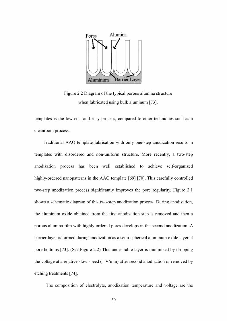
templates is the low cost and easy process, compared to other techniques such as a
cleanroom process.
Traditional AAO template fabrication with only one-step anodization results in
templates with disordered and non-uniform structure. More recently, a two-step
anodization process has been well established to achieve self-organized
highly-ordered nanopatterns in the AAO template [69] [70]. This carefully controlled
two-step anodization process significantly improves the pore regularity. Figure 2.1
shows a schematic diagram of this two-step anodization process. During anodization,
the aluminum oxide obtained from the first anodization step is removed and then a
porous alumina film with highly ordered pores develops in the second anodization. A
barrier layer is formed during anodization as a semi-spherical aluminum oxide layer at
pore bottoms [73]. (See Figure 2.2) This undesirable layer is minimized by dropping
the voltage at a relative slow speed (1 V/min) after second anodization or removed by
etching treatments [74].
The composition of electrolyte, anodization temperature and voltage are the
Figure 2.2 Diagram of the typical porous alumina structure
when fabricated using bulk aluminum [73].
31
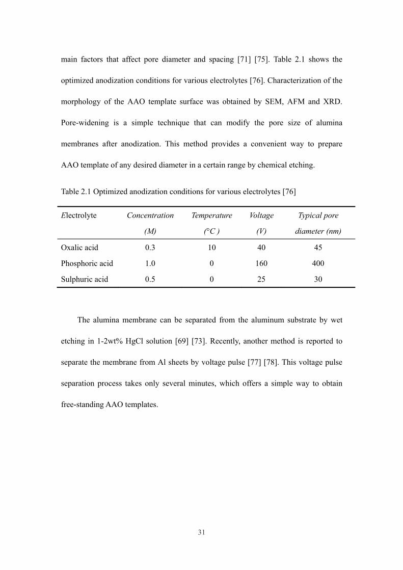
main factors that affect pore diameter and spacing [71] [75]. Table 2.1 shows the
optimized anodization conditions for various electrolytes [76]. Characterization of the
morphology of the AAO template surface was obtained by SEM, AFM and XRD.
Pore-widening is a simple technique that can modify the pore size of alumina
membranes after anodization. This method provides a convenient way to prepare
AAO template of any desired diameter in a certain range by chemical etching.
Table 2.1 Optimized anodization conditions for various electrolytes [76]
The alumina membrane can be separated from the aluminum substrate by wet
etching in 1-2wt% HgCl solution [69] [73]. Recently, another method is reported to
separate the membrane from Al sheets by voltage pulse [77] [78]. This voltage pulse
separation process takes only several minutes, which offers a simple way to obtain
free-standing AAO templates.
Electrolyte Concentration
(M)
Temperature
(°C )
Voltage
(V)
Typical pore
diameter (nm)
Oxalic acid 0.3 10 40 45
Phosphoric acid 1.0 0 160 400
Sulphuric acid 0.5 0 25 30

32
2.2 Methodology of electrode design
2.2.1 Preliminary electrode design
The object of the research is to develop a general design for biosensors. Glucose
biosensor is selected as the model system to verify the design of the biosensors.
Figure 2.3 shows the preliminary design of glucose biosensor. In this design, there are
four main steps: AAO template fabrication, gold deposition, GOx immobilization and
characterization. Porous highly ordered AAO templates are prepared by two-step
anodization. Deposited gold on both sides of electrodes surfaces serve as contacts and
prevent non-specific adhesion of GOx on the surface. And then GOx is adsorbed to
the sidewalls of the porous alumina membrane’s nanopores. Electrochemical
characterization provides feedback for optimizing the nanostructured electrode device.
Cyclic Voltammetry (CV) in [Fe(CN)6]3– /[Fe(CN)6]4– system is carried out to
determine the minimum thickness of Au coating as effective contact. Finally, study of
Design of Electrode
Gold Deposition
AAO Template Fabrication
GOx Immobilization
Characterization
Biomedical Application
Figure 2.3 Methodology of preliminary electrochemical
glucose biosensor design.
33
enzymatic redox in glucose solutions by CV is attempted.
One method of GOx immobilization is to adsorb several layers of protein
nanotubes (known as binding agents) onto the pore of AAO template and then attach
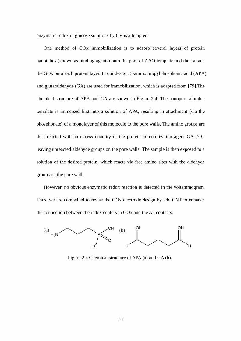
the GOx onto each protein layer. In our design, 3-amino propylphosphonic acid (APA)
and glutaraldehyde (GA) are used for immobilization, which is adapted from [79].The
chemical structure of APA and GA are shown in Figure 2.4. The nanopore alumina
template is immersed first into a solution of APA, resulting in attachment (via the
phosphonate) of a monolayer of this molecule to the pore walls. The amino groups are
then reacted with an excess quantity of the protein-immobilization agent GA [79],
leaving unreacted aldehyde groups on the pore walls. The sample is then exposed to a
solution of the desired protein, which reacts via free amino sites with the aldehyde
groups on the pore wall.
However, no obvious enzymatic redox reaction is detected in the voltammogram.
Thus, we are compelled to revise the GOx electrode design by add CNT to enhance
the connection between the redox centers in GOx and the Au contacts.
Figure 2.4 Chemical structure of APA (a) and GA (b).
(b) (a) H2N P
OH
HOO
H
OH
H
OH
34
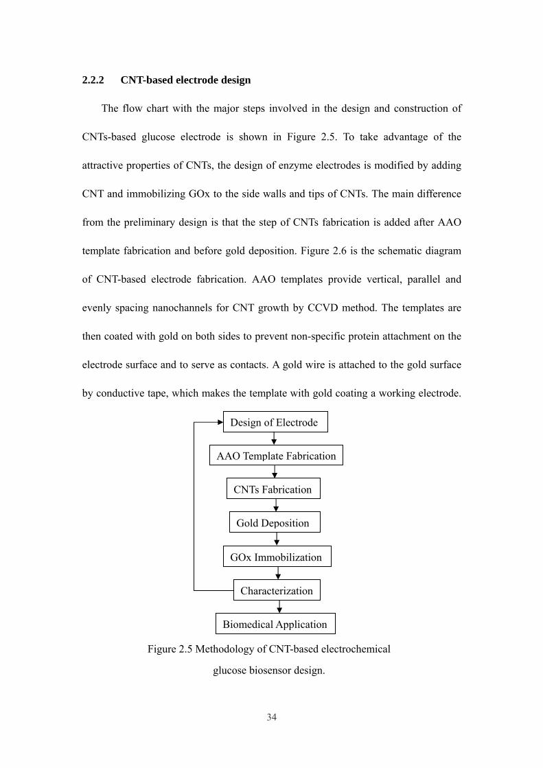
2.2.2 CNT-based electrode design
The flow chart with the major steps involved in the design and construction of
CNTs-based glucose electrode is shown in Figure 2.5. To take advantage of the
attractive properties of CNTs, the design of enzyme electrodes is modified by adding
CNT and immobilizing GOx to the side walls and tips of CNTs. The main difference
from the preliminary design is that the step of CNTs fabrication is added after AAO
template fabrication and before gold deposition. Figure 2.6 is the schematic diagram
of CNT-based electrode fabrication. AAO templates provide vertical, parallel and
evenly spacing nanochannels for CNT growth by CCVD method. The templates are
then coated with gold on both sides to prevent non-specific protein attachment on the
electrode surface and to serve as contacts. A gold wire is attached to the gold surface
by conductive tape, which makes the template with gold coating a working electrode.
Design of Electrode
Gold Deposition
CNTs Fabrication
AAO Template Fabrication
GOx Immobilization
Characterization
Biomedical Application
Figure 2.5 Methodology of CNT-based electrochemical
glucose biosensor design.

35
Figure 2.6 (b) shows the GOx immobilization process. Ideally, GOx molecules are
immobilized on the side walls and tips of CNTs. For future study, further
characterization of this CNT based glucose biosensor by CV and is desirable.
Figure 2.6 Schematic diagrams of CNT-based electrode fabrication (a) and GOx
immobilization (b).
(b)
+ binding agents ★ glucose oxidase
(a)
36
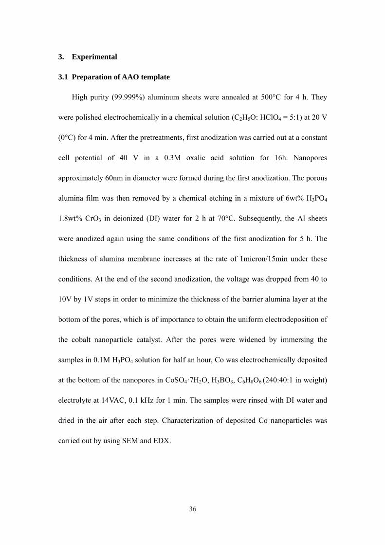
3. Experimental
3.1 Preparation of AAO template
High purity (99.999%) aluminum sheets were annealed at 500°C for 4 h. They
were polished electrochemically in a chemical solution (C2H5O: HClO4 = 5:1) at 20 V
(0°C) for 4 min. After the pretreatments, first anodization was carried out at a constant
cell potential of 40 V in a 0.3M oxalic acid solution for 16h. Nanopores
approximately 60nm in diameter were formed during the first anodization. The porous
alumina film was then removed by a chemical etching in a mixture of 6wt% H3PO4
1.8wt% CrO3 in deionized (DI) water for 2 h at 70°C. Subsequently, the Al sheets
were anodized again using the same conditions of the first anodization for 5 h. The
thickness of alumina membrane increases at the rate of 1micron/15min under these
conditions. At the end of the second anodization, the voltage was dropped from 40 to
10V by 1V steps in order to minimize the thickness of the barrier alumina layer at the
bottom of the pores, which is of importance to obtain the uniform electrodeposition of
the cobalt nanoparticle catalyst. After the pores were widened by immersing the
samples in 0.1M H3PO4 solution for half an hour, Co was electrochemically deposited
at the bottom of the nanopores in CoSO4·7H2O, H3BO3, C6H8O6 (240:40:1 in weight)
electrolyte at 14VAC, 0.1 kHz for 1 min. The samples were rinsed with DI water and
dried in the air after each step. Characterization of deposited Co nanoparticles was
carried out by using SEM and EDX.

37
3.2 Study of gold deposition
Two groups of samples were prepared for characterization optimized Au
thickness. Group A consisted of two commercial templates purchased from Whatman
Company with pore diameter of 200nm and membrane diameter of 13mm. Group B
consisted of the empty AAO templates fabricated by two-step anodization in our lab.
To remove the barrier layer of the homemade AAO template, the sample was
immersed in 0.5M phosphoric acid solution at room temperature for 1 h before Au
deposition. 1 wt% HgCl2 solution was used to separate the AAO template from the Al
substrate underneath. Gold deposition was carried out to form a continuous coating on
both sides for both groups, following the schematic steps shown in Figure 3.1.
For Group A, templates were coated with thickness of 5nm, 20nm or 50nm Au on
the front side and 5nm thick Au on the back side using an e-beam evaporator. During
the e-beam evaporation, the base pressure was controlled between 4-5x10⁻⁷ torr and
the evaporation rate of 1 Å/s. Gold wires were then attached to the front surfaces of
the templates with conductive tape, to form the working electrodes.
CV studies were carried out using a BAS 100 B/W Potentiostat C3 cell in a
three-electrode system. The template served as a working electrode, a platinum wire
as a counter electrode, and a Ag/AgCl electrode as a reference electrode.
Figure 3.1 Schematic diagram of preparing AAO templates with gold coating.
38
3.3 Preliminary biosensor construction
The AAO templates with gold coated on both sides were immersed in a 5 mM
APA solution at 5.8 pH for 24 hours. Afterwards, the samples were immersed in a 2.5
wt% solution of GA for 12 hours. Finally, the GOx were deposited by vacuum
filtration of the 10 mg/mL GOx solution through the membrane, using a Millipore
mini-vacuum system. A gold wire was attached to the top of the AAO template by
conductive taping.
39
3.4 Carbon nanotubes growth
CCVD method was applied to grow CNTs in the porous alumina film. To
investigate the appropriate conditions for CNT growth by CCVD method, two sets of
experiments were carried out. First, empty commercial templates were utilized for
CNT growth in pure C2H2 gas for 10 minutes, 30 minutes and 1 hour, without catalyst.
Thermal cleaning conditions were examined in order to remove junk carbon deposited
on the surface of AAO templates. Second, a mixture of 10 vol% acetylene and 90 vol%
N2 has been employed to grow CNTs for 1 h, 2h, 4h and 10 h in home-made AAO
templates, using electrodeposited cobalt as a catalyst.
Figure 3.2 shows a schematic of the CNTs growth conditions. The samples,
were placed in a tube furnace and were heated up to 600 °C at a rate of 10 °C /min
with a flow rate of 60 sccm of pure nitrogen. At 600 °C, N2 was replaced by pure CO
to reduce any cobalt oxides. After 1 hour, the gas was changed to pure acetylene or a
mixture gas of 10 vol% acetylene and 90 vol% N2. In order to find the proper growth
time for CNTs, the growth was carried out over different period. After CNT growth,
the furnace was cooled down to room temperature in pure N2 atmosphere.
Figure 3.2 Schematic diagram of CNTs growth conditions.
Room Temperature
Temperature (°C)
600
Time (h)
10°C/min
CO for 1h Growth time
40
For SEM observation, the AAO template was wet etched in a mixture solution of
6wt% H3PO4 and 1.8wt% CrO3 for 5 hours to partially expose the CNTs. For TEM
observation, the CNTs were released by removing the alumina template in 0.5M
NaOH solution. The collected CNTs were rinsed by DI water using centrifuge and
dispersed in ethanol by sonication. TEM samples were made by dropping a few drops
of the ethanol solution containing the CNTs onto copper grids.
41
4. Results and discussions
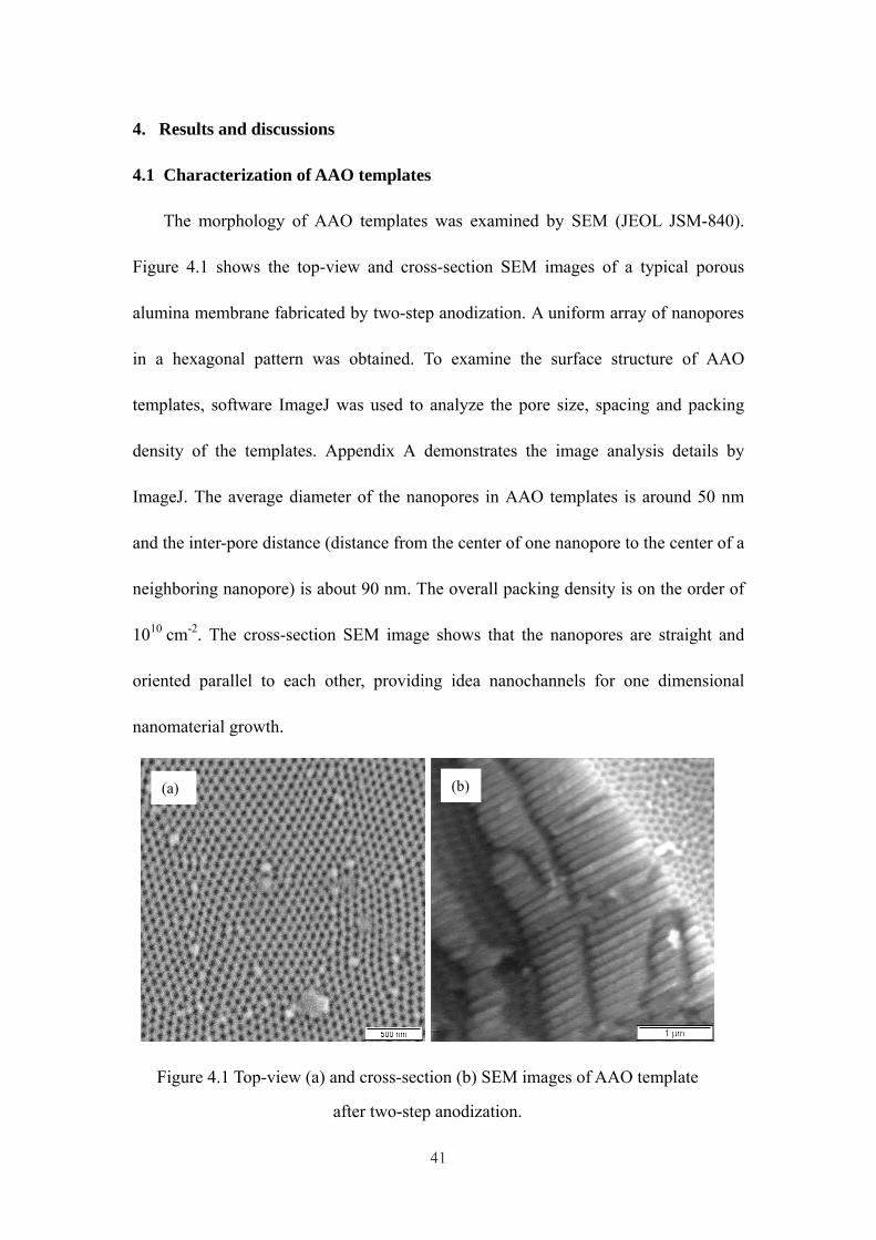
4.1 Characterization of AAO templates
The morphology of AAO templates was examined by SEM (JEOL JSM-840).
Figure 4.1 shows the top-view and cross-section SEM images of a typical porous
alumina membrane fabricated by two-step anodization. A uniform array of nanopores
in a hexagonal pattern was obtained. To examine the surface structure of AAO
templates, software ImageJ was used to analyze the pore size, spacing and packing
density of the templates. Appendix A demonstrates the image analysis details by
ImageJ. The average diameter of the nanopores in AAO templates is around 50 nm
and the inter-pore distance (distance from the center of one nanopore to the center of a
neighboring nanopore) is about 90 nm. The overall packing density is on the order of
1010 cm-2. The cross-section SEM image shows that the nanopores are straight and
oriented parallel to each other, providing idea nanochannels for one dimensional
nanomaterial growth.
Figure 4.1 Top-view (a) and cross-section (b) SEM images of AAO template
after two-step anodization.
(a) (b)
42
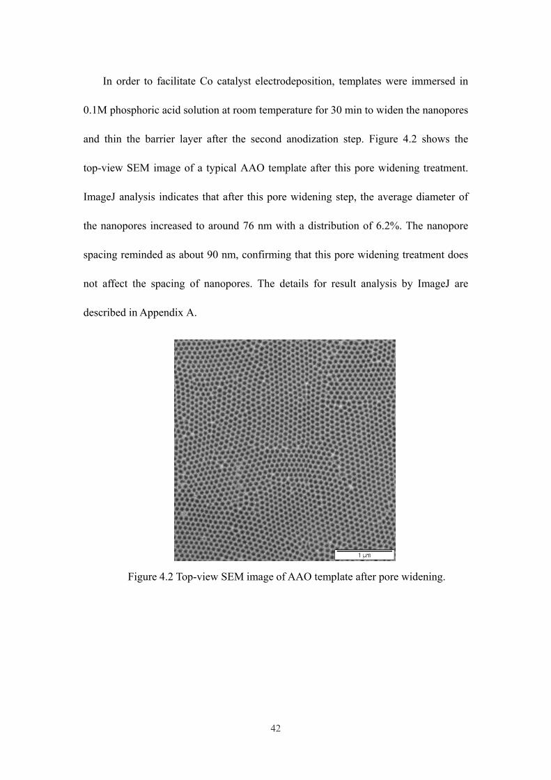
In order to facilitate Co catalyst electrodeposition, templates were immersed in
0.1M phosphoric acid solution at room temperature for 30 min to widen the nanopores
and thin the barrier layer after the second anodization step. Figure 4.2 shows the
top-view SEM image of a typical AAO template after this pore widening treatment.
ImageJ analysis indicates that after this pore widening step, the average diameter of
the nanopores increased to around 76 nm with a distribution of 6.2%. The nanopore
spacing reminded as about 90 nm, confirming that this pore widening treatment does
not affect the spacing of nanopores. The details for result analysis by ImageJ are
described in Appendix A.
Figure 4.2 Top-view SEM image of AAO template after pore widening.
43
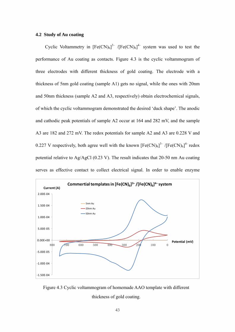
4.2 Study of Au coating
Cyclic Voltammetry in [Fe(CN)6]3– /[Fe(CN)6]4– system was used to test the
performance of Au coating as contacts. Figure 4.3 is the cyclic voltammogram of
three electrodes with different thickness of gold coating. The electrode with a
thickness of 5nm gold coating (sample A1) gets no signal, while the ones with 20nm
and 50nm thickness (sample A2 and A3, respectively) obtain electrochemical signals,
of which the cyclic voltammogram demonstrated the desired ‘duck shape’. The anodic
and cathodic peak potentials of sample A2 occur at 164 and 282 mV, and the sample
A3 are 182 and 272 mV. The redox potentials for sample A2 and A3 are 0.228 V and
0.227 V respectively, both agree well with the known [Fe(CN)6]3– /[Fe(CN)6]4– redox
potential relative to Ag/AgCl (0.23 V). The result indicates that 20-50 nm Au coating
serves as effective contact to collect electrical signal. In order to enable enzyme
Figure 4.3 Cyclic voltammogram of homemade AAO template with different
thickness of gold coating.
‐1.50E‐04
‐1.00E‐04
‐5.00E‐05
0.00E+00
5.00E‐05
1.00E‐04
1.50E‐04
2.00E‐04
0100200300400500600700800
Current (A)
Potential (mV)
Commertial templates in [Fe(CN)6]3– /[Fe(CN)6]4– system
5nm Au
20nm Au
50nm Au
44
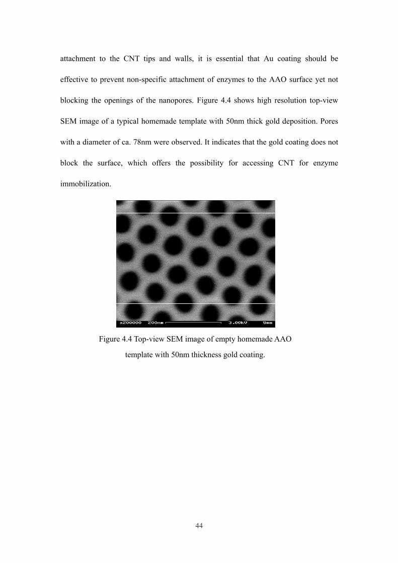
attachment to the CNT tips and walls, it is essential that Au coating should be
effective to prevent non-specific attachment of enzymes to the AAO surface yet not
blocking the openings of the nanopores. Figure 4.4 shows high resolution top-view
SEM image of a typical homemade template with 50nm thick gold deposition. Pores
with a diameter of ca. 78nm were observed. It indicates that the gold coating does not
block the surface, which offers the possibility for accessing CNT for enzyme
immobilization.
Figure 4.4 Top-view SEM image of empty homemade AAO
template with 50nm thickness gold coating.
45
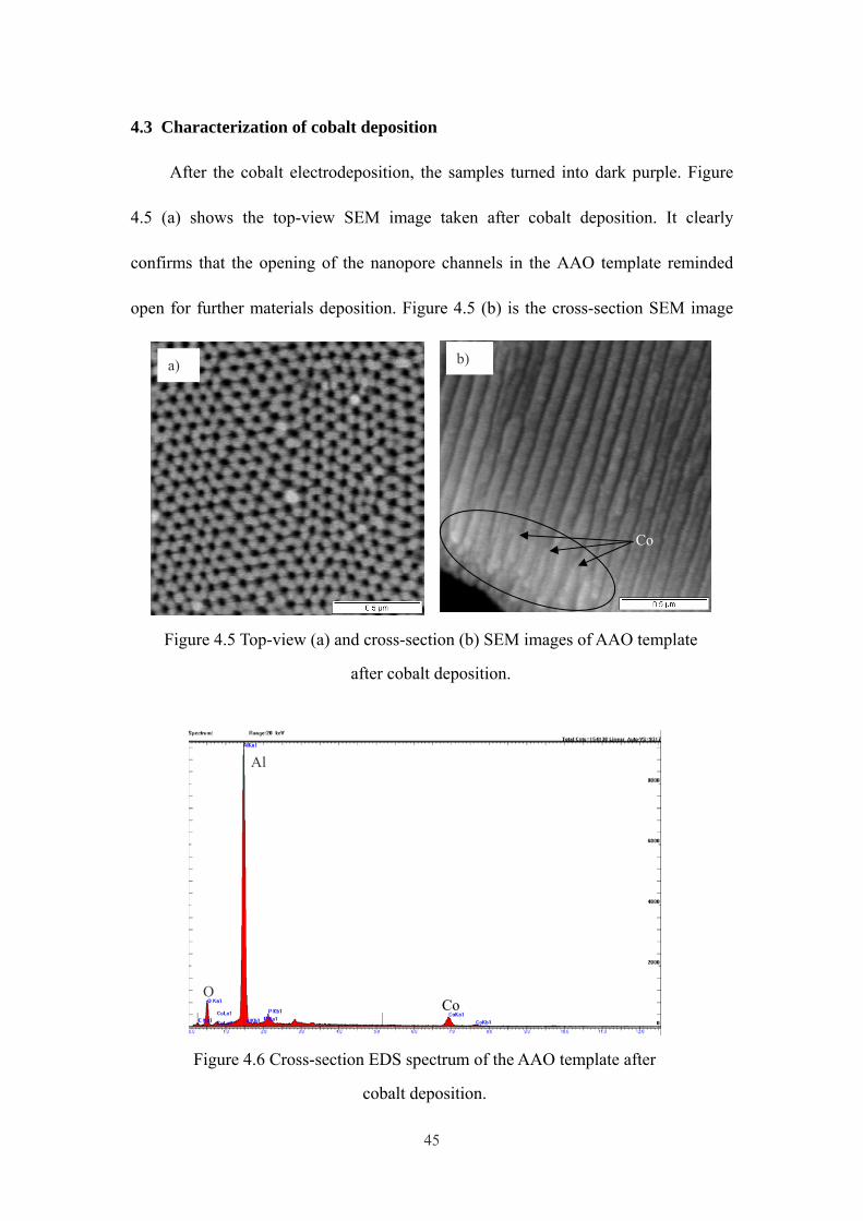
4.3 Characterization of cobalt deposition
After the cobalt electrodeposition, the samples turned into dark purple. Figure
4.5 (a) shows the top-view SEM image taken after cobalt deposition. It clearly
confirms that the opening of the nanopore channels in the AAO template reminded
open for further materials deposition. Figure 4.5 (b) is the cross-section SEM image
a) b)
Co
Figure 4.5 Top-view (a) and cross-section (b) SEM images of AAO template
after cobalt deposition.
Co
Al
O
Figure 4.6 Cross-section EDS spectrum of the AAO template after
cobalt deposition.
46
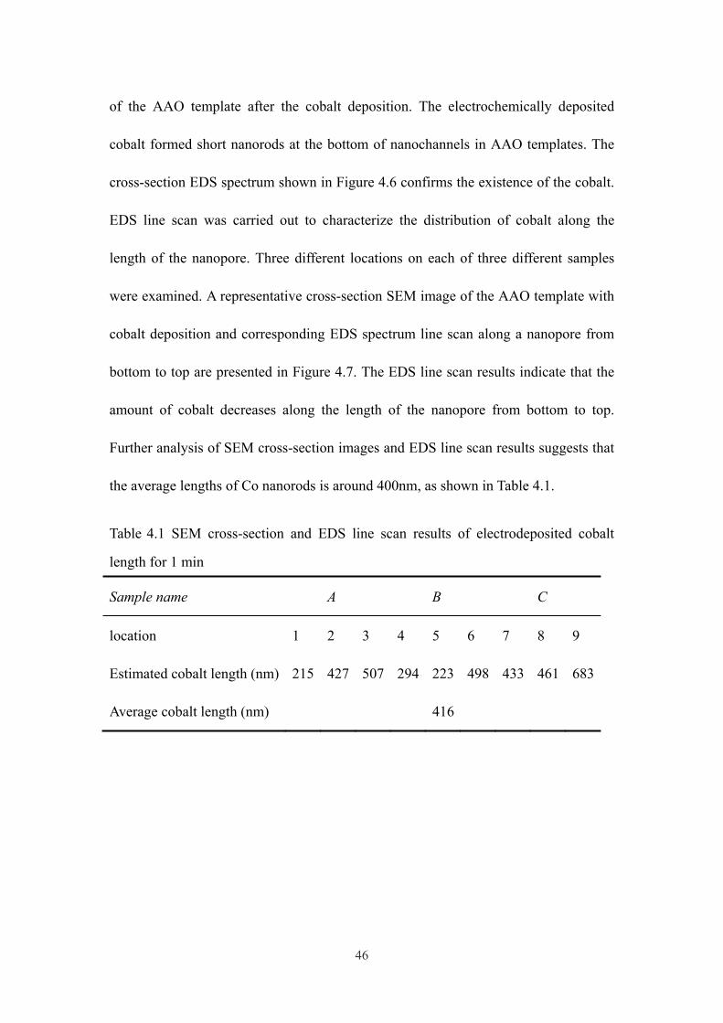
of the AAO template after the cobalt deposition. The electrochemically deposited
cobalt formed short nanorods at the bottom of nanochannels in AAO templates. The
cross-section EDS spectrum shown in Figure 4.6 confirms the existence of the cobalt.
EDS line scan was carried out to characterize the distribution of cobalt along the
length of the nanopore. Three different locations on each of three different samples
were examined. A representative cross-section SEM image of the AAO template with
cobalt deposition and corresponding EDS spectrum line scan along a nanopore from
bottom to top are presented in Figure 4.7. The EDS line scan results indicate that the
amount of cobalt decreases along the length of the nanopore from bottom to top.
Further analysis of SEM cross-section images and EDS line scan results suggests that
the average lengths of Co nanorods is around 400nm, as shown in Table 4.1.
Table 4.1 SEM cross-section and EDS line scan results of electrodeposited cobalt
length for 1 min
Sample name A B C
location 1 2 3 4 5 6 7 8 9
Estimated cobalt length (nm) 215 427 507 294 223 498 433 461 683
Average cobalt length (nm) 416
Co Co
47
Figure 4.7 Cross-section SEM image of the AAO template after cobalt deposition (a)
and EDS spectrum line scan along the length of the nanopore from bottom to top.
1500nm
Co - 76
Co
(a) (b) tensity
48
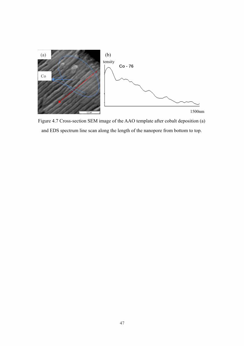
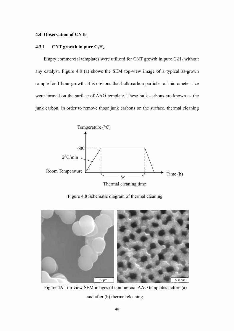
4.4 Observation of CNTs
4.3.1 CNT growth in pure C2H2
Empty commercial templates were utilized for CNT growth in pure C2H2 without
any catalyst. Figure 4.8 (a) shows the SEM top-view image of a typical as-grown
sample for 1 hour growth. It is obvious that bulk carbon particles of micrometer size
were formed on the surface of AAO template. These bulk carbons are known as the
junk carbon. In order to remove those junk carbons on the surface, thermal cleaning
Figure 4.9 Top-view SEM images of commercial AAO templates before (a)
and after (b) thermal cleaning.
Figure 4.8 Schematic diagram of thermal cleaning.
Room Temperature Time (h)
2°C/min
Thermal cleaning time
Temperature (°C)
600
49
conditions were studied. The cleaning procedure employed a temperature profile
shown in Figure 4.8. The templates were heated to 600°C at 2 °C/min and kept for
various periods in air. Three different thermal cleaning periods were tested: 10 min,
30min and 1h. It was found that 1 hour was needed to thoroughly clean the surface
with junk carbon. Junk carbon on the AAO surface was removed partially for 10 min
or 30 min. Figure 4.9 (b) shows the top-view SEM images of commercial AAO
templates after 1 hour thermal cleaning. However, no CNTs were observed after this
thermal cleaning process. Even though there were reports suggesting that AAO
template can sever as a weak catalyst for CNT CCVD growth [80], under the growth
conditions in our study, the catalytic effect might be too weak to result in significant
CNT growth. In addition, large size junk carbon might have been formed from the
beginning of the growth due to the easy access to the top surface and blocked the
passage to the inside of nanopore channels for CNT growth. Thus, a second group of
samples were fabricated by employing a mixture of 10 vol% acetylene and 90 vol%
N2 to grow CNTs for 1 h, 2h, 4h and 10 h in home-made AAO templates, using
electrodeposited cobalt as catalyst.
50
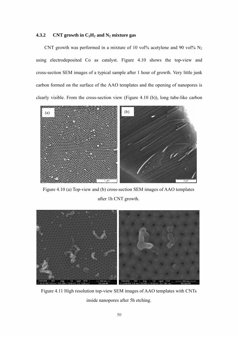
4.3.2 CNT growth in C2H2 and N2 mixture gas
CNT growth was performed in a mixture of 10 vol% acetylene and 90 vol% N2
using electrodeposited Co as catalyst. Figure 4.10 shows the top-view and
cross-section SEM images of a typical sample after 1 hour of growth. Very little junk
carbon formed on the surface of the AAO templates and the opening of nanopores is
clearly visible. From the cross-section view (Figure 4.10 (b)), long tube-like carbon
Figure 4.11 High resolution top-view SEM images of AAO templates with CNTs
inside nanopores after 5h etching.
Figure 4.10 (a) Top-view and (b) cross-section SEM images of AAO templates
after 1h CNT growth.
(a) (b)
51
was observed.
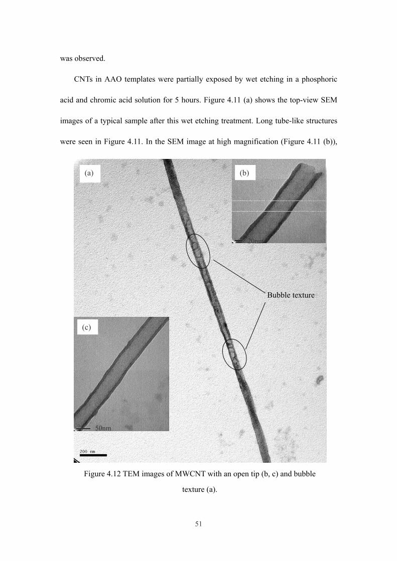
CNTs in AAO templates were partially exposed by wet etching in a phosphoric
acid and chromic acid solution for 5 hours. Figure 4.11 (a) shows the top-view SEM
images of a typical sample after this wet etching treatment. Long tube-like structures
were seen in Figure 4.11. In the SEM image at high magnification (Figure 4.11 (b)),
Figure 4.12 TEM images of MWCNT with an open tip (b, c) and bubble
texture (a).
Bubble texture
20nm
(b)
50nm
(a)
(c)
52
in addition to these long tube-like structures, it was observed that shape of the
opening of nanopore channels changed to irregular shapes compared with samples
without CNT growth (Figure 4.10 (a)) and the diameter of the opening of nanopore
channels decreased to 30 nm (analysis by ImageJ) due to the growth of CNTs along
the inner wall of nanopore channels. Further CNTs characterization was carried out
using TEM (JEOL 100kV TEM). CNTs were released by dissolving the templates in
NaOH solution. Figure 4.12 (a) is the TEM image of MWCNT with a hollow shape.
Figure 4.12 (b) shows that the tip of as fabricated MWCNTs is open. Figure 4.12
shows that the diameter of the MWCNTs is around 60nm, which agrees with the
diameter of the pore size of the AAO template. The length of MWCNTs varies up to
the micron scale.
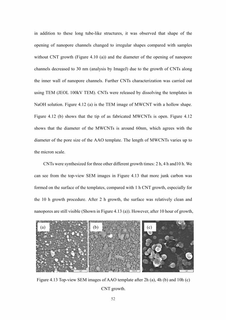
CNTs were synthesized for three other different growth times: 2 h, 4 h and10 h. We
can see from the top-view SEM images in Figure 4.13 that more junk carbon was
formed on the surface of the templates, compared with 1 h CNT growth, especially for
the 10 h growth procedure. After 2 h growth, the surface was relatively clean and
nanopores are still visible (Shown in Figure 4.13 (a)). However, after 10 hour of growth,
Figure 4.13 Top-view SEM images of AAO template after 2h (a), 4h (b) and 10h (c)
CNT growth.
(a) (b) (c)
53
only large carbon particles can be resolved by top-view SEM observation. It was
confirmed that the thermal cleaning procedure we developed were effective to remove
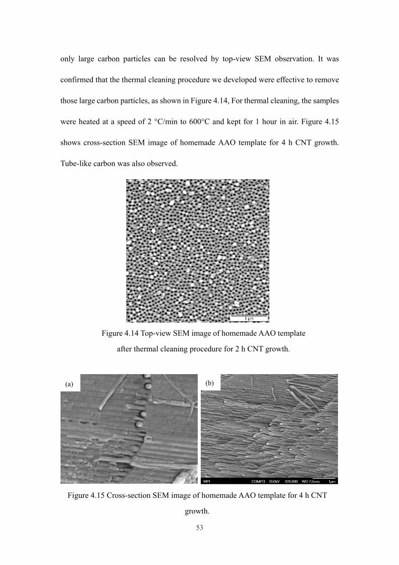
those large carbon particles, as shown in Figure 4.14, For thermal cleaning, the samples
were heated at a speed of 2 °C/min to 600°C and kept for 1 hour in air. Figure 4.15
shows cross-section SEM image of homemade AAO template for 4 h CNT growth.
Tube-like carbon was also observed.
Figure 4.15 Cross-section SEM image of homemade AAO template for 4 h CNT
growth.
Figure 4.14 Top-view SEM image of homemade AAO template
after thermal cleaning procedure for 2 h CNT growth.
(a) (b)

54
5. Conclusions
A general design of electrochemical biosensors based on vertically aligned CNTs
arrays has been developed. Electrochemically deposited Co was employed as the
catalyst to facilitate the CNT growth. MWCNTs with open tips were successfully
fabricated by catalytic chemical vapor deposition. The fabricated MWCNTs were
characterized using SEM and TEM. CV testing in both [Fe(CN)6]3– /[Fe(CN)6]4–
system and glucose system show the redox reactions have been observed. Gold
deposition of 20nm thickness on the surface of AAO was confirmed to be sufficient to
provide effective contact for electrochemical measurements.
55
6. Future work
Our success in well aligned CNT growth by CCVD and preliminary work on
constructing nanostructured biosensors provided unique opportunities for further
study of:
1. The growth mechanisms of CNT by CCVD;
2. Highly controllable immobilization of GOx on well-aligned CNT arrays;
3. Synthesis of ultrasensitive glucose nanobiosensor;
4. Electrochemical behaviors of this novel glucose nanobiosensors by CV;
5. Immobilization of other biomolecules such as enzymes on well-aligned CNT;
6. Synthesis and electrochemical characterization of nanobiosensors;
7. The general design of the nanobiosensors based on vertically aligned CNT
arrays.
56
7. References
[1]. Iijima, S. Nature 1991, 354, 56-8.
[2]. Iijima, S.; Ichihashi, T. Nature 1993, 363, 603.
[3]. Bethune, D. S.; Klang, C. H.; de Vries, M. S.; Gorman, G.; Savoy, R.; Vazquez,
J.; Beyers, R. Nature 1993, 363, 605.
[4]. Dresselhaus, M. S.; Dresselhaus, G.; Hofmann, M. Vib. Spectrosc. 2007, 45,
71-81.
[5]. Martel, R.; Schmidt, T.; Shea, H. R.; Hertel, T.; Avouris, P., Applied Physics
Letters 1998, 73, 2447.
[6]. Cheung, C. L.; Hafner, J. H.; Lieber, C. M. Proc. Natl. Acad. Sci. U.S.A. 2000, 79,
3809-13.
[7]. Wong, S. S.; Joselevich, E.; Woolley, A. T.; Cheung, C. L.; Lieber, C. M. Nature
1998, 394, 52-5.
[8]. Bhushan, B., Ed. Springer handbook of nanotechnology New York:
Spinger-Verlag Berlin Heidelberg, 2003.
[9]. Tsang , S.; de Oliveira, P.; Davis, J. J.; Green, M. L. H.; Hill, H. A. O. Chem.
Phys. Lett. 1996, 249, 413-22.
[10]. Monthioux, M.; Smith, B. W.; Vurteaux, B.; Claye, A.; Fischer, J. E.; Luzzi, D.
E.; Carbon 2001, 39, 1251-72.
[11]. Ebbesen, T. W.; Ajayan, P. M. Nature 1992, 358, 220-2.
[12]. Saito, R.; Fujita, M.; Dresselhaus, G.; Dresselhaus, Appl. Phys. Lett. 1992, 60,
2204.
57
[13]. Hamada, N.; Sawada, S.; Oshiyama, A. Phys. Rev. Lett. 1992, 68, 1579-81.
[14]. Wildoer, J. W. G.; Venema, L. C.; Rinzier, A. G.; Smalley, R. E.; Dekker, C.
Nature 1998, 391, 59.
[15]. Odom, T. W.; Huang, J.-L.; Kim, P.; Lieber, C. M. Nature 1998, 391, 62.
[16]. Poole Jr., C. P.; Owens, F. J. Introduction to Nanotechnology Hoboken: John
Wiley & Sons, Inc. 2003.
[17]. Berber, S.; Kwon, Y.; Tomanek, D. Phys. Rev. Lett. 2002, 84, 4613-6.
[18]. Baughman, R. H.; Zakhidov, A. A.; de Heer, W. A. Science 2002, 297, 787-92.
[19]. Yu, M.; Lourie, O.; Dyer, M. J.; Moloni, K.; Kelly, T. F.; Ruoff, R. S. Science
2000, 287, 637-40.
[20]. Walters, D. A.; Ericson, L. M.; Casavant, M. J.; Liu, J.; Colbert, D. T.; Smith, K.
A.; Smalley, R. E. Appl. Phys. Lett. 1999, 74, 3803-5.
[21]. Yakobson, B. I.; Brabec, C. J.; Bernholc, J. Phys. Rev. Lett. 1996, 76, 2511-4.
[22]. Wong, E. W.; Sheehan, P. E.; Lieber, C. M. Science 1997, 277, 1971-5.
[23]. Gao, R.; Wang, Z. L.; Bai, Z.; de Heer, W. A.; Dai, L.; Gao, M. Phys. Rev. Lett.
2000, 85, 622-5.
[24]. Zhao, J.; Buldum, A.; Han, J.; Ping Lu, J. Phys. Rev. Lett. 2000, 85, 1706-9.
[25]. Cadek, M.; Coleman, J. N.; Barron, V. Appl. Phys. Lett. 2002, 81, 5123-5.
[26]. Tasca, F.; Gorton, L.; Wagner, J. B.; Nöll, G. Biosens. Bioelectron. 2008, 24,
272-8.
[27]. Cheung, C. L.; Hafner, J. H.; Odom, T. W.; Kim, K.; Lieber, C. M. Appl. Phys.
Lett. 2000, 76, 3136-8.
58
[28]. Bianco, A.; Kostarelos, K.; Prato, M. Curr. Opin. Chem. Biol. 2005, 9, 674-9.
[29]. Zhao, Q.; Gan, Z.; Zhuang, Q. Electroanalysis 2002, 14, 1609-13.
[30]. Wei, T.; Fan, Z.; Luo, G.; Wei, F.; Zhao, D.; Fan, J. Mater. Res. Bull. 2008, 43,
2806-9.
[31]. Guo, T.; Nikolaev, P.; Rinzler, A. G.; Tomanek, D.; Colbert, D. T.; Smalley, R. E.
Chem. Phys. Lett. 1995, 99, 10694-7.
[32]. Guo, T.; Nikolaev, P.; Thess, A.; Colbert, D. T.; Smalley, R. E. Chem. Phys. Lett.
1995, 243, 49-54.
[33]. Thess, A.; Lee, R.; Nikolaev, P.; Dai, H.; Petit, P.; Robert, J.; Xu, C.; Lee, Y. H.;
Kim, S. G.; Rinzler, A. G.; Colbert, D. T.; Scuseria, G. E.; Tománek, D.; Fischer,
J. E. and Smalley; R. E. Science 1996, 273, 483.
[34]. Li, J.; Papadopoulos, C.; Xu, J. M.; Moskovits, M. Appl. Phys. Lett. 1999, 75,
367-9.
[35]. Yuan, Z.; Huang, H.; Liu, L.; Fan, S. Chem. Phys. Lett. 2001, 345, 39-43.
[36]. Kong, J.; Cassel, A. M.; Dai, H. Chem. Phys. Lett. 1998, 292, 567-74.
[37]. Lee, J. S.; Gu, G. H.; Kim, H.; Jeong, K. S.; Bae, J.; Suh, J. Chem. Mater., 2001,
13, 2387-91
[38]. Yun, Y.; Shanov, V.; Tu, Y.; Subramaniam, S.; Schulz, M. J. J. Phys. Chem. B
2006, 110, 23920-5.
[39]. Cass, A. E. G. Biosensors: A Practical Approach Oxford: IRL Press, 1990.
[40]. Eggins, Brian Biosensors: An Introduction, Teubner: John Wiley & Sons, Ltd and
B. G. 2006.
59
[41]. Clark, L. C.; Lyons, C. Ann. N. Y. Acad. Sci. 1962, 102, 29.
[42]. Wang, J. Electroanalysis 2001, 13, 983-8.
[43]. Goodsell, D. S. Molecule of the Month 2006.
http://www.rcsb.org/pdb/static.do?p=education_discussion/molecule_of_the_mon
th/molecule_list_2006.html
[44]. Degani, Y.; Heller, A. J. Phys. Chem. 1987, 91, 1285-9.
[45]. Kim, J.; Jia, H.; Wang, P. Biotech. Adv., 2006, 24, 296-308.
[46]. Wang, J.; Musameh, M.; Lin, Y. J. Am. Chem. Soc. 2003, 125, 2408-9.
[47]. Lin, Y.; Lu, F.; Tu, Y.; Ren, Z. Nano Lett. 2004, 4, 191-5.
[48]. Zou, Y.; Xiang, C.; Sun, L.; Xu, F. Electrochim. Acta 2008, 53, 4089-95.
[49]. Cao, Z.; Jiang, X.; Xie, Q.; Yao, S. Biosens. Bioelectron. 2008, 24, 222-7.
[50]. Wu, B.; Hou, S.; Yu, M.; Qin, X.; Li, S.; Chen, Q. DNLM, 2008, In Press.
[51]. Wang, J. Electroanalysis 2005, 17, 7-14.
[52]. Vamvakakl, V.; Tsagarakl, K.; Chanlotakls, N. Anal. Chem. 2006 78, 5538-42.
[53]. Withey, G. D.; Lazareck, A. D.; Tzolov, M. B.; Yin, A.; Aich, P.; Yeh, J. I.; Xu, J.
M. Biosens. Bioelectron. 2006, 21, 1560-5.
[54]. Gouveia-Caridade, C.; Pauliukaite, R.; Brett, C. M. A. Electrochim. Acta 2008,
53, 6732-9.
[55]. Patolsky, F.; Weizmann, Y. and Willner, I. Angew. Chem. Int. Ed. 2004, 43,
2113.
[56]. Li, J.; Wang, Y.; Qiu, J.; Sun, D.; Xia, X. Anal. Bioanal. Chem. 2005, 383,
918-22.
60
[57]. Signore, M. A.; Rizzo, A.; Rossi, R.; Piscopiello, E.; Luccio, T. D.; Capodieci, L.;
Dikonimos, T.; Giorgi, R. Diamond Relat. Mater. 2008, In Press.
[58]. Newbury, D. E.; Williams, D. B. Acta. Mater. 2000, 48, 323-46.
[59]. Wang, Z. L., Ed. Characterization of Nanophase Materials Weinheim:
WILEY-VCH Verlag GmbH, 2000.
[60]. Ge, M.; Sattler, K. Appl. Phys. Lett. 1994, 65, 2284-6.
[61]. Zhang, Z.; Lieber, C. M. Appl. Phys. Lett. 1993, 62, 2792-4.
[62]. Rao, A. M.; Eklund, P. C.; Bandow, S.; Thess, A.; Smalley, R. E. Nature 1950
1997, 388, 257-9.
[63]. Dresselhaus, M. S.; Dresselhaus, G.; Satio, R. Jorio, A. Phys. Rep. 2005, 409,
47-99.
[64]. Dresselhaus, M. S.; Villalpando-Paez, F.; Samsonidze, G. G.; Chou, S. G.;
Dresselhaus, G.; Jiang, J.; Saito, R.; Souza Filho, A. G.; Jorio, A.; Endo, M.; Kim,
Y. -A.; Physica. E 2007, 37, 81-7.
[65]. Wang, J. Analytical electrochemistry 3rd ed., Hoboken: John Wiley & Sons, Inc.
2006.
[66]. Bard, A.J.; Faulkner, L.R. Electrochemical Methods: Fundamentals and
Applications. New York: John Wiley & Sons, 2nd Edition, 2000.
[67]. Anton, A. H.; Sayre, D. F. J. Pharmacol. Exp. Ther. 1962, 138, 360-75.
[68]. Chik, H.; Xu, J. M. Mater. Sci. Eng. R Rep. 2004, 43, 103-36.
[69]. Masuda, H.; Fukuda, K. Science 1995, 268, 1466-8.
61
[70]. Masuda, H.; Yamada, H.; Satoh, M.; Asoh, H.; Nakao, M.; Tamamura, T. Appl.
Phys. Lett. 1997, 71, 2770-2.
[71]. Li, A. P.; Müller, F.; Birner, A.; Nielsch, K.; Gösele, U. J. Appl. Phys. 1998, 84,
6023-6.
[72]. Jessensky, O.; Müller, F.; Gösele, U. J. Electrochem. Soc. 1998, 145, 3735-40.
[73]. Crouse, D.; Lo, Y.; Miller, A. E.; Croue, M. Appl. Phys. Lett. 2000, 76, 49-51.
[74]. Liang, J.; Chik, H.; Yin, A.; Xu, J. J. Appl. Phys. 2001, 91, 2544-6.
[75]. Wang, X.; Han, G. Microelectronic Engineering 2003, 66, 166-70.
[76]. Liang, J.; Chik, H.; Xu, J. IEEE J Quantum Electron, 2005, 8, 998-1008.
[77]. Yuan, J. H.; He, F. H.; Sun, D. C.; Xia, X. H. Chem. Mater. 2004, 16, 1841-4.
[78]. Zhao, S.; Chan, K.; Yelon, A.; Veres, T. Nanotechnology, 2007, 18, 245304-8.
[79]. Hou, S.; Wang, J.; Martin, C. R. Nano Lett. 2005, 5, 231-4.
[80]. Kyotani, T.; Tsai, L.; Tomita, A. Chem. Mater. 1996, 8, 2109-13.
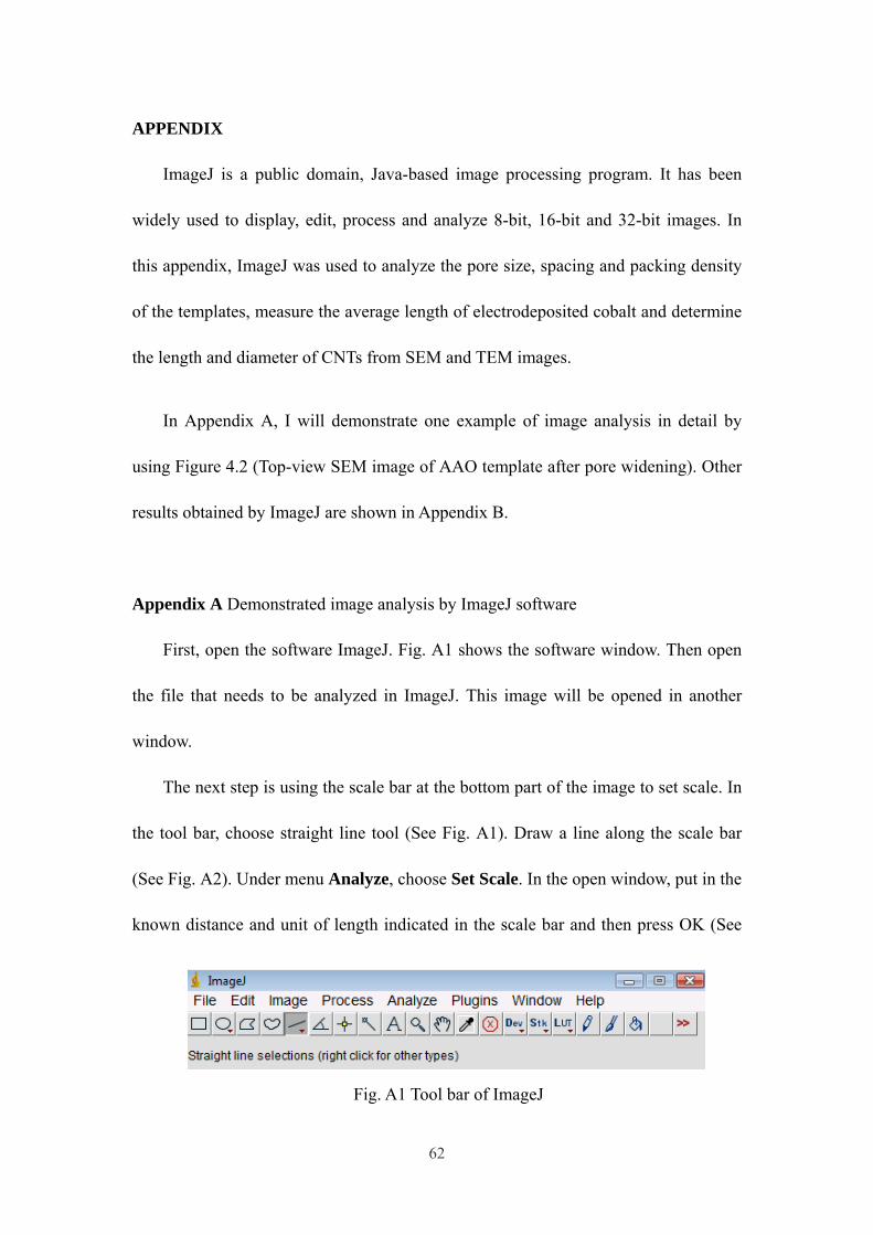
62
APPENDIX
ImageJ is a public domain, Java-based image processing program. It has been
widely used to display, edit, process and analyze 8-bit, 16-bit and 32-bit images. In
this appendix, ImageJ was used to analyze the pore size, spacing and packing density
of the templates, measure the average length of electrodeposited cobalt and determine
the length and diameter of CNTs from SEM and TEM images.
In Appendix A, I will demonstrate one example of image analysis in detail by
using Figure 4.2 (Top-view SEM image of AAO template after pore widening). Other
results obtained by ImageJ are shown in Appendix B.
Appendix A Demonstrated image analysis by ImageJ software
First, open the software ImageJ. Fig. A1 shows the software window. Then open
the file that needs to be analyzed in ImageJ. This image will be opened in another
window.
The next step is using the scale bar at the bottom part of the image to set scale. In
the tool bar, choose straight line tool (See Fig. A1). Draw a line along the scale bar
(See Fig. A2). Under menu Analyze, choose Set Scale. In the open window, put in the
known distance and unit of length indicated in the scale bar and then press OK (See
Fig. A1 Tool bar of ImageJ

63
Fig. A2).
Fig. A2 Set scale in ImageJ
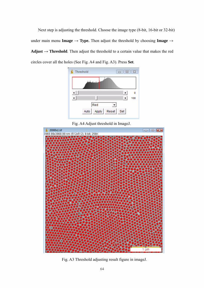
64
Next step is adjusting the threshold. Choose the image type (8-bit, 16-bit or 32-bit)
under main menu Image → Type. Then adjust the threshold by choosing Image →
Adjust → Threshold. Then adjust the threshold to a certain value that makes the red
circles cover all the holes (See Fig. A4 and Fig. A3). Press Set.
Fig. A4 Adjust threshold in ImageJ.
Fig. A3 Threshold adjusting result figure in imageJ.
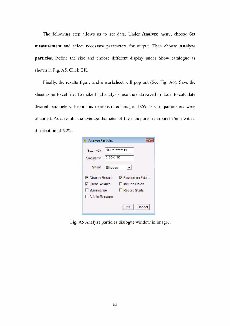
65
The following step allows us to get data. Under Analyze menu, choose Set
measurement and select necessary parameters for output. Then choose Analyze
particles. Refine the size and choose different display under Show catalogue as
shown in Fig. A5. Click OK.
Finally, the results figure and a worksheet will pop out (See Fig. A6). Save the
sheet as an Excel file. To make final analysis, use the data saved in Excel to calculate
desired parameters. From this demonstrated image, 1869 sets of parameters were
obtained. As a result, the average diameter of the nanopores is around 76nm with a
distribution of 6.2%.
Fig. A5 Analyze particles dialogue window in imageJ.
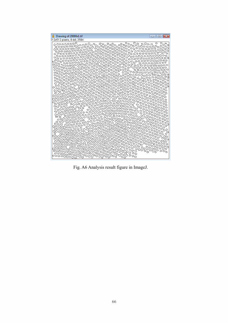
66
Fig. A6 Analysis result figure in ImageJ.

67
Appendix B Other image analysis by ImageJ
Using the same analysis procedures demonstrated above, Figure 4.1 (Top-view
SEM images of AAO template after two-step anodization), Figure 4.4 (Top-view SEM
image of empty homemade AAO template with 50nm thickness gold coating) and
Figure 4.11 (b) (top-view SEM images of AAO templates with CNTs inside nanopores
after 5h etching) were examined by ImageJ.
Fig. B1 shows the analysis results image of Figure 4.1. The average diameter of
the nanopores in AAO templates is around 50 nm and the inter-pore distance (distance
from the center of one nanopore to the center of a neighboring nanopore) is about
90nm. The overall packing density is on the order of 1010 cm-2.
Fig. B1 ImageJ analysis results image of AAO template after
pore widening.
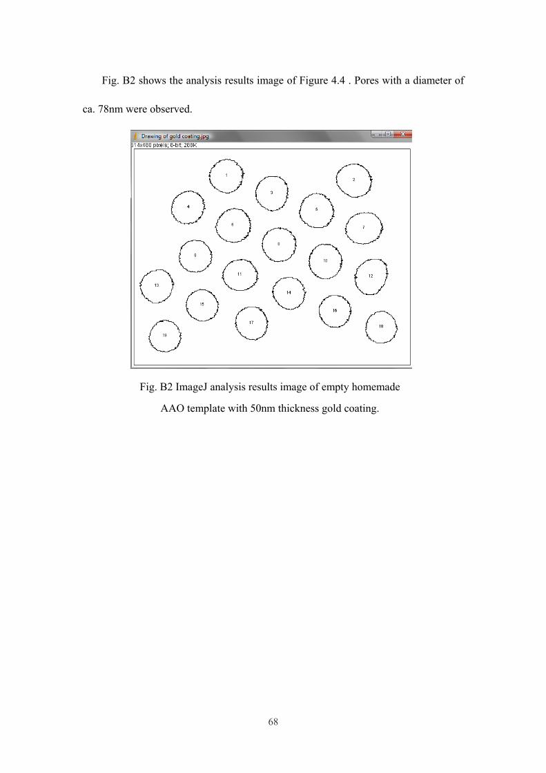
68
Fig. B2 shows the analysis results image of Figure 4.4 . Pores with a diameter of
ca. 78nm were observed.
Fig. B2 ImageJ analysis results image of empty homemade
AAO template with 50nm thickness gold coating.
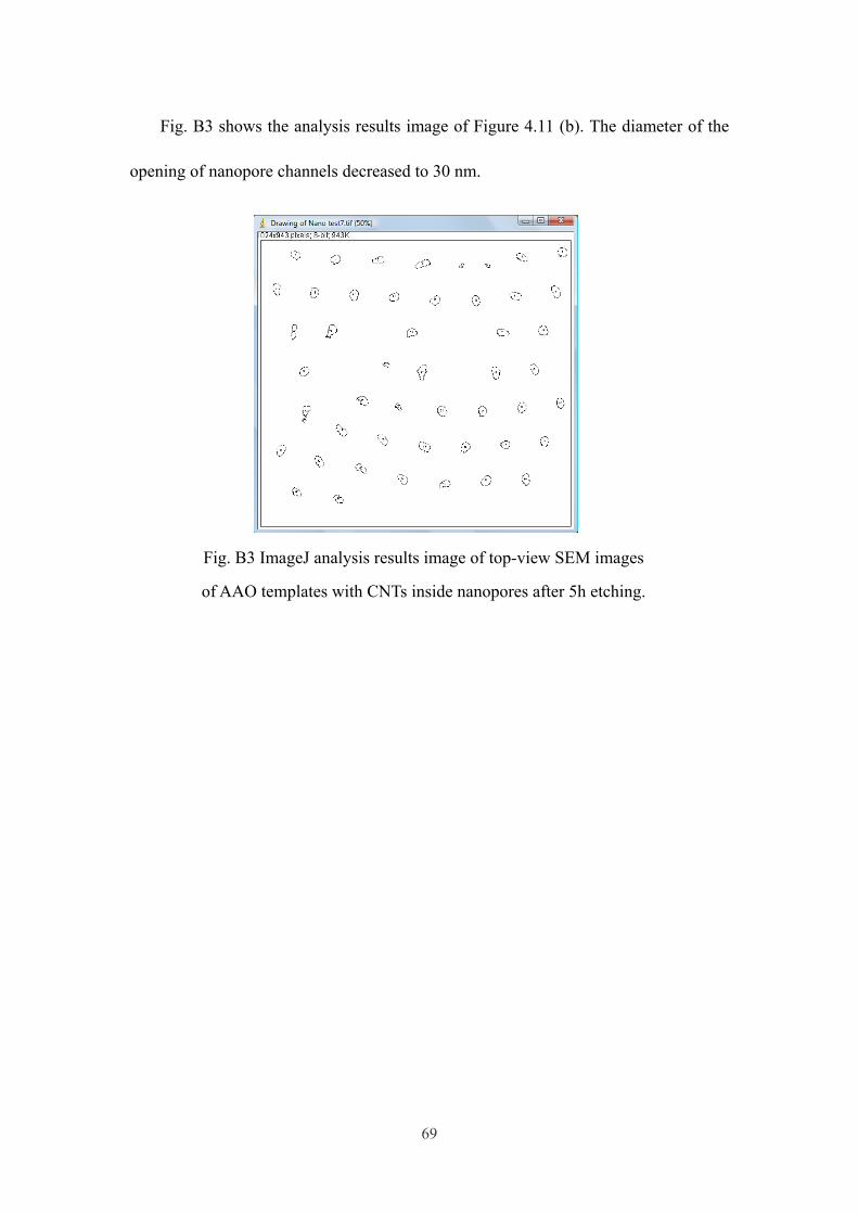
69
Fig. B3 shows the analysis results image of Figure 4.11 (b). The diameter of the
opening of nanopore channels decreased to 30 nm.
Fig. B3 ImageJ analysis results image of top-view SEM images
of AAO templates with CNTs inside nanopores after 5h etching.