fabrication and characterization of micro and nano … and...fabrication and characterization of...
TRANSCRIPT
Fabrication and Characterization ofMicro and Nano Scale SiC UV Photodetectors
Author:Ludwig Östlund
Supervisors:Dr. Qin Wang (Acreo)
Dr. Wlodek Kaplan (Acreo)
Examiner:Professor Sebastian Lourdudoss
(KTH)
StockholmNovember, 2011


Abstract
The focus of this master thesis work is on the fabrication of micro- and nano-scale metal-semiconductor-metal silicon carbide (SiC) UV photodetectors and subsequent electrical andoptical evaluation of the fabricated devices. The UV photodetectors have significant potentialto address the needs of many applications such as detection of corona discharge and flames, in-dustrial machine viewing, and bacteria in water or paper mills. Micro-scale devices in 4H-SiCand 6H-SiC have been fabricated successfully with good photoresponse and low dark current.Reduction in size of the 4H-SiC UV detectors from micro-scale to nano-scale has been achievedby the use of nano imprint lithography (NIL). The performance of these nano-devices havebeen characterized, and experiment results reveal good photo sensitivity at very low appliedbiases.
III

IV

Acknowledgments
First I would like to thank Acreo for founding this project.
A big thanks to my very supportive supervisor Qin Wang, who have made the time at Acreoa true pleasure.
Thanks to my supervisor Wlodek Kaplan and my examiner Sebastian Lourdudoss for allsupport.
Thanks to all lab personal and SiC people for all help throughout this project: SusanneAlmqvist, Helena Strömberg, Reza Nikpars, Malin Gustavsson , Romain Esteve, Sergey Re-shanov, Andy Zhang, Jang-Kwon Lim, Mietek Bakowski and Adolf Schöner.
I would also want to thank all my student friends at Acreo and KTH for being so supportiveand such nice company during this project: Boban Gavric, Ali Asadollahi, Sandine van Frank,Xun Li (Anneli), Norbert Kwietniewski, Laiq Hussain and Marine Disdero.
Also thanks to all other Acreo and IR-Nova personal that have not been mentioned abovefor being helpful and very nice company.
Finally thanks to my family, to my dear girlfriend and near friends who always have beena great support.
V

VI
Contents
Abstract III
Acknowledgments V
Contents VII
List of Figures VIII
List of Tables X
List of Abbreviations XII
1 Introduction 11.1 Project description . . . . . . . . . . . . . . . . . . . . . . . . . . . . . . . . . . 11.2 Extended Work . . . . . . . . . . . . . . . . . . . . . . . . . . . . . . . . . . . . 21.3 UV Detector Applications . . . . . . . . . . . . . . . . . . . . . . . . . . . . . . 2
2 SiC Materials and Devices 42.1 Silicon Carbide . . . . . . . . . . . . . . . . . . . . . . . . . . . . . . . . . . . . 4
2.1.1 SiC Polytypes and Properties . . . . . . . . . . . . . . . . . . . . . . . . 52.1.2 Epitaxial Growth . . . . . . . . . . . . . . . . . . . . . . . . . . . . . . . 5
2.2 Metal-Semiconductor-Metal Photodetector . . . . . . . . . . . . . . . . . . . . . 62.2.1 Schottky Barrier Diode . . . . . . . . . . . . . . . . . . . . . . . . . . . 62.2.2 MSM Junction as Photo Detector . . . . . . . . . . . . . . . . . . . . . . 10
3 Lithography Techniques 123.1 Photolithography . . . . . . . . . . . . . . . . . . . . . . . . . . . . . . . . . . . 123.2 Nano Imprint Lithography . . . . . . . . . . . . . . . . . . . . . . . . . . . . . . 13
3.2.1 Principles of NIL . . . . . . . . . . . . . . . . . . . . . . . . . . . . . . . 133.2.2 NIL Stamp Fabrication by e-beam Lithography . . . . . . . . . . . . . . 153.2.3 Stamp Replication by NIL . . . . . . . . . . . . . . . . . . . . . . . . . . 153.2.4 UV Curable Nano Imprint Resists . . . . . . . . . . . . . . . . . . . . . 153.2.5 Adhesion . . . . . . . . . . . . . . . . . . . . . . . . . . . . . . . . . . . 16
4 Fabrication of Micro Scale Devices 174.1 Fabrication Process . . . . . . . . . . . . . . . . . . . . . . . . . . . . . . . . . . 17
4.1.1 Cleaning . . . . . . . . . . . . . . . . . . . . . . . . . . . . . . . . . . . . 174.1.2 Anti Reflective Coating . . . . . . . . . . . . . . . . . . . . . . . . . . . 17
VII
4.1.3 Photolithography Patterning . . . . . . . . . . . . . . . . . . . . . . . . 184.1.4 Metallization . . . . . . . . . . . . . . . . . . . . . . . . . . . . . . . . . 194.1.5 Lift-off . . . . . . . . . . . . . . . . . . . . . . . . . . . . . . . . . . . . . 20
4.2 Fabricated Micro Scale MSM Devices . . . . . . . . . . . . . . . . . . . . . . . . 20
5 Fabrication of Nano Scale Devices 245.1 Preparation . . . . . . . . . . . . . . . . . . . . . . . . . . . . . . . . . . . . . . 24
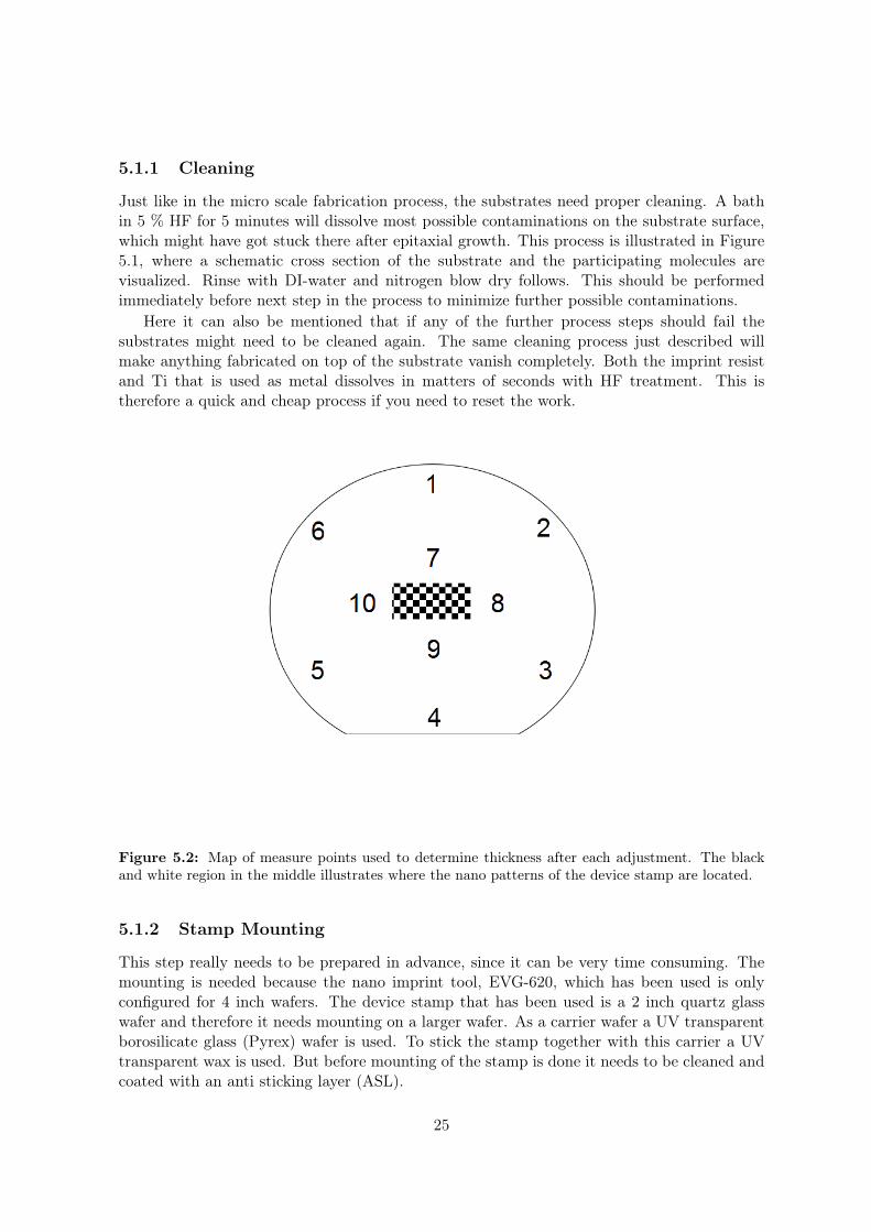
5.1.1 Cleaning . . . . . . . . . . . . . . . . . . . . . . . . . . . . . . . . . . . . 255.1.2 Stamp Mounting . . . . . . . . . . . . . . . . . . . . . . . . . . . . . . . 25
5.2 Fabrication Process . . . . . . . . . . . . . . . . . . . . . . . . . . . . . . . . . . 285.2.1 Metallization . . . . . . . . . . . . . . . . . . . . . . . . . . . . . . . . . 285.2.2 Nano Imprint Lithography . . . . . . . . . . . . . . . . . . . . . . . . . . 295.2.3 Residual Resist Etch by Dry Etching . . . . . . . . . . . . . . . . . . . . 295.2.4 Metal Etch . . . . . . . . . . . . . . . . . . . . . . . . . . . . . . . . . . 305.2.5 Resist Stripping by Dry Etch . . . . . . . . . . . . . . . . . . . . . . . . 32
5.3 Fabricated Nano Scale MSM Devices . . . . . . . . . . . . . . . . . . . . . . . . 34
6 Characterization of Devices 376.1 Material Characterization . . . . . . . . . . . . . . . . . . . . . . . . . . . . . . 38
6.1.1 Scanning Electron Microscopy . . . . . . . . . . . . . . . . . . . . . . . . 386.1.2 Atomic Force Microscopy . . . . . . . . . . . . . . . . . . . . . . . . . . 396.1.3 Doping Profile . . . . . . . . . . . . . . . . . . . . . . . . . . . . . . . . 406.1.4 Optical Characteristics of SiC Epitaxial Layers on Substrates . . . . . . 42
6.2 Spectral Response for Micro Scale MSM Devices . . . . . . . . . . . . . . . . . 446.3 Photo Response and I-V Characteristics . . . . . . . . . . . . . . . . . . . . . . 45
6.3.1 Micro Scale Devices . . . . . . . . . . . . . . . . . . . . . . . . . . . . . 456.3.2 Nano Scale Devices . . . . . . . . . . . . . . . . . . . . . . . . . . . . . . 48
7 Conclusions and Future Work 507.1 Conclusions . . . . . . . . . . . . . . . . . . . . . . . . . . . . . . . . . . . . . . 507.2 Future Work . . . . . . . . . . . . . . . . . . . . . . . . . . . . . . . . . . . . . 51
Bibliography 52
A 4H- and 6H-SiC UV photodetectors 54
B A theoretical and experimental comparison of 4H- and 6H-SiC MSM UVphotodetectors 58
VIII
List of Figures
2.1 Band diagrams of metal and n-type semiconductor apart. . . . . . . . . . . . . 72.2 Band diagrams of a Schottky contact between metal and n-type semiconductor. 72.3 The change of built in voltage as a function of the donor doping concentration
in 4H-SiC. . . . . . . . . . . . . . . . . . . . . . . . . . . . . . . . . . . . . . . . 82.4 Depletion region width vs. applied bias in a Ni/4H-SiC Schottky diode for
several donor concentrations. . . . . . . . . . . . . . . . . . . . . . . . . . . . . 92.5 MSM device biased and exposed to photons. . . . . . . . . . . . . . . . . . . . . 11
3.1 Droplet disposal. The stamp is then pressed against the surface. . . . . . . . . . 133.2 The resist is cured by UV light. . . . . . . . . . . . . . . . . . . . . . . . . . . . 143.3 Stamp is released from the surface, leaving the nano pattern in the resist. . . . 14
4.1 SiC substrate with epilayers and SiO2. . . . . . . . . . . . . . . . . . . . . . . . 184.2 Patterning of the resist with a photo mask. . . . . . . . . . . . . . . . . . . . . 184.3 The SiO2 is etched down to the epitaxial layers. . . . . . . . . . . . . . . . . . . 194.4 Metal is applied. . . . . . . . . . . . . . . . . . . . . . . . . . . . . . . . . . . . 194.5 The resist and remaining metal is removed in the lift-off process, here is the
cross section of the final product. . . . . . . . . . . . . . . . . . . . . . . . . . . 204.6 Mask design at chip level. . . . . . . . . . . . . . . . . . . . . . . . . . . . . . . 214.7 MSM device sketch. . . . . . . . . . . . . . . . . . . . . . . . . . . . . . . . . . 214.8 Optical microscope image of a symmetric MSM device on 4H-SiC. . . . . . . . . 22
5.1 Cleaning of the surface with diluted hydrofluoric acid. . . . . . . . . . . . . . . 245.2 Map of measure points used to determine thickness after each adjustment. The
black and white region in the middle illustrates where the nano patterns of thedevice stamp are located. . . . . . . . . . . . . . . . . . . . . . . . . . . . . . . 25
5.3 A 3D sketch of an adjusted stamp made in MATLAB. The ten measure pointsshown in Figure 5.2 has been used while the other points are approximatedfrom the slopes between them. Unit for this sketch is meter. . . . . . . . . . . . 26
5.4 A picture captured from an optical microscope of a test imprint after satisfyingadjustments of the stamp mounting. . . . . . . . . . . . . . . . . . . . . . . . . 27
5.5 Deposition of titanium on substrate surface by e beam evaporation in a highvacuum chamber. . . . . . . . . . . . . . . . . . . . . . . . . . . . . . . . . . . . 28
5.6 Dry etching of the remaining resist down to the metal by plasma with gasesSF6 and O2. . . . . . . . . . . . . . . . . . . . . . . . . . . . . . . . . . . . . . . 29
5.7 Patterned resist on top of the metal before wet etch. . . . . . . . . . . . . . . . 305.8 Remaining metal structures after wet etch. . . . . . . . . . . . . . . . . . . . . . 31
IX
5.9 Dry selective etching of the metal down to the substrate. . . . . . . . . . . . . . 325.10 Dry etching to strip any remaining of the resist. . . . . . . . . . . . . . . . . . . 335.11 Complete nano devices with varying finger width and finger spacing. . . . . . . 335.12 Complete nano devices cross section. . . . . . . . . . . . . . . . . . . . . . . . . 345.13 Map of devices from the 2 inch stamp. . . . . . . . . . . . . . . . . . . . . . . . 355.14 Sketch of circular shaped nano MSM devices. . . . . . . . . . . . . . . . . . . . 35
6.1 An array of 2 by 5 MSM photo detectors by SEM capture. . . . . . . . . . . . . 376.2 Cross section SEM capture of 4H-SiC epitaxial layers. . . . . . . . . . . . . . . 386.3 Cross section SEM capture of 6H-SiC epitaxial layers. . . . . . . . . . . . . . . 396.4 Surface of epitaxially grown 6H-SiC. . . . . . . . . . . . . . . . . . . . . . . . . 406.5 Doping profile of n-type 4H-SiC epitaxial layers. . . . . . . . . . . . . . . . . . . 416.6 Doping profile of p-type 6H-SiC epitaxial layers. . . . . . . . . . . . . . . . . . . 416.7 Fabricated devices on 4H-SiC (left) and 6H-SiC (right). . . . . . . . . . . . . . 426.8 Optical absorption spectra for 4H- and 6H-SiC substrates with epitaxial layers.
A-F corresponds to different measurement points. . . . . . . . . . . . . . . . . . 426.9 Spectral response for Micro Scale 4H- and 6H-SiC MSM Photodetectors. . . . . 446.10 Photoresponse in symmetrical electrode type MSM. . . . . . . . . . . . . . . . . 466.11 Photoresponse in symmetrical electrode type MSM. . . . . . . . . . . . . . . . . 476.12 Photoresponse in asymmetric electrode type MSM. . . . . . . . . . . . . . . . . 486.13 Photoresponse nano scale MSM photo detectors. . . . . . . . . . . . . . . . . . 48
X

List of Tables
2.1 Important properties of SiC polytypes . . . . . . . . . . . . . . . . . . . . . . . 5
4.1 Specifications of micro scale MSM devices investigated in this work. . . . . . . . 22
5.1 Nano scale MSM photo detector specifications. . . . . . . . . . . . . . . . . . . 36
XI

List of AbbreviationsAFM atomic force microscopeARC anti reflective coatingASL anti sticking layerC-V capacitance/voltageCVD chemical vapor depositionDI-water deionized waterIR infra redI-V current/voltageLPCVD low pressure chemical vapor depositionMSM metal semiconductor metalNIL nano imprint lithographyQD quantum dotsSEM scanning electron microscopeUV ultravioletUV-LED ultraviolet light emitting diode
XII

Chapter 1
Introduction
In this chapter background and content of this master thesis project will be described alongwith some thoughts about applications for UV detectors.
1.1 Project description
This master thesis work has been carried out at Acreo, Kista, during October 2010 until May2011. Acreo is a research institute which has been active in the SiC field since 1993 and coversall aspects of SiC technology from device design to epitaxy and device manufacturing. Acreohas also been developing the NIL technique since 2005. This has provided a good base forthe fabrication of nano scale devices. For example, nano scale UV detectors based on GaNhave been demonstrated [1]. The main goal of this project has been to fabricate silicon car-bide (SiC) based metal-semiconductor-metal ultraviolet (UV) photodetectors by nano imprintlithography (NIL). Subsequent electrical and optical measurements of the fabricated devicesshould be done to characterize the product. Nano-scale MSM UV photodetectors on SiC hasnot been fabricated before. The NIL fabrication technique will bring the detectors from microscale to nano scale, where higher sensitivity and faster time response can be expected [2]. Inthe long-term, it is believed that the effect of shrinking SiC device sizes to nano scale will havea dramatic effect on the performance of devices and open new avenues for the design of nextgeneration SiC components and compact systems. UV detectors have significant potential toaddress the needs of many applications such as detection of corona discharge and flames, in-dustrial machine viewing, and bacteria in water or paper mills. This can be achieved throughthe use of nanotechnology, which is an important enabling technology for the production of acomplete detection system with high sensitivity and stability.
My work has involved the following tasks:
• Design of the SiC epitaxial structure and growth, together with experienced personnelat Acreo
• Clean room processing of the nano scale SiC UV detectors using NIL, reactive ion etchingand metallization techniques
• Measurement of electrical and optical performance of the fabricated devices
• Written report
1
1.2 Extended Work
Originally the plan was five months for this project, but due to extension of the work also thetime plan was extended. In order to compare the nano scale to micro scale devices, it wasdecided that micro scale MSM photo detectors should also be fabricated and characterized.The fabrication of these detectors was done by ordinary UV photo lithography, metallizationand lift off processes.
Another extended work carried out was further development of NIL process based on existNIL technique developed at Acreo since 2005. New NIL resist, adhesion promoters, wafer-scaleNIL resist coating techniques and stamp replications were investigated to optimize stabilityand high throughput of the NIL process. Also, utilizing successfully optimized NIL process inthis work, photodetectors based on other semiconductors than SiC as Schottky photodiodesin nano scale were pursued.
In summary, following tasks were involved as extended work in frame of this thesis:
• Designing and processing of micro scale SiC UV detectors using photolithography, met-allization and lift off
• Processing of NIL techniques in Electrum Laboratory
• Fabrication of nano scale GaSb, Si, InSb and InAs quantum dots (QD) devices usingNIL
Due to success and great performance in the fabricated micro scale SiC UV detectorsan article was written and presented at the 16th Semiconducting and Insulating MaterialsConference (SIMC-XVI) in Stockholm, Kista 2011. This article can be read in Appendix A.Difference in device performance for different substrates also lead to a simulation work byJ.-K. Lim at Acreo. This article is included in Appendix B.
1.3 UV Detector Applications
The target for UV detectors are many. They can be used to observe naturally occurring UVlight such as from the sun and reflections from it, or by exposure from various UV light sources.It is important not to mix UV reflection with fluorescence since pure UV reflection cannot beseen directly by a human eye. What you usually can see when emitting UV radiation on forexample white colored materials, is fluorescence. The high energy UV radiation is absorbedand reflected with less energy in the visible range. To actually see the pure UV light reflectedyou need a UV detector.
Applications for UV detectors are many. There are for example flame detection systemscombining infrared (IR) and UV detection lower the rate of false alarms and also to characterizewhat is burning. For instance, black body radiation from a thermal source can more easily besorted out. This kind of spectroscopy could also be used for military applications.
One way of water bacteria treatment is to illuminate water with high power UV lightwhich eliminates bacterias. These bacterias are also visible in the UV range, which make UVdetectors a good way of monitoring the water quality.
In astronomy it can be important to view distant objects in different wavelength rangessuch as UV. Stars, including our own sun, look very different in the IR, visible, UV and X-rayranges. Also in nature you can find variation in appearance looking in UV. Birds and insects
2

can for example see UV light, enabling them to see other colors in flowers, feathers and organicmaterials.
Bringing the UV photodetectors to nano scale should increase time response. Fast timeresponse could be used for example in UV fiber optics to increase speed in data transfer.
3
Chapter 2
SiC Materials and Devices
This chapter will give the reader the basic information about the material silicon carbideneeded for this project. The theory of the metal-semiconductor-metal (MSM) photodetectordevices will be briefly described. MSM devices are based on Schottky diodes why they alsoare mentioned in this chapter, not to mix up with pn-diodes.
2.1 Silicon Carbide
SiC is a group IV semiconductor material, which is a hot topic nowadays. It has a lot ofdifferent applications in electronics and mechanics due to its properties and advantages. It isalmost as hard as diamond (9-9.5 on the Mohs scale, 10 for diamond) [3] and in low dopingconcentrations it is almost fully transparent visually. Electrical devices in this material canbe operated at very high temperatures, over 500 degrees celsius. SiC is also very tolerant toheavy high energy radiation. This makes the material suitable for space applications where itwould need no shielding mechanism, which otherwise increases the total mass of the devices.Low mass and high tolerance to heat and external radiation makes it perfect for extremeenvironments such as outer space. This is just one application and we could go on make thelist very long.
Moreover due to its wide band gap SiC is very suitable for UV photo detection whereas itcorresponds very well to the limit between visible and UV light, 400 nm. Therefore no externalfilters would be needed in order to block light in the visible range for the detector. Opticalfilters might also reduce the intensity of incoming UV light. The construction of a detectorwill be simpler and the fabrication process will therefore be cheaper, while the performanceshould be better.
In former projects at Acreo [1] GaN has been used as semiconductor for MSM UV detectors.SiC is an indirect bandgap material while GaN has a direct band gap and usually directbandgap materials are preferred as photo detectors. However SiC is a much more maturematerial when it comes to quality, both dislocation density and numbers of crystal domainsare many order of magnitudes lower in SiC. Also the electron affinity is higher in GaN thanin SiC making the Schottky barrier height smaller in GaN, resulting in a higher dark current.
4
2.1.1 SiC Polytypes and Properties
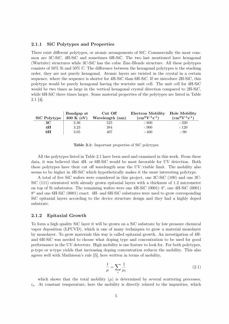
There exist different polytypes, or atomic arrangements of SiC. Commercially the most com-mon are 3C-SiC, 4H-SiC and sometimes 6H-SiC. The two last mentioned have hexagonal(Wurtzite) structures while 3C-SiC has the cubic Zinc-Blende structure. All these polytypesconsists of 50% Si and 50% C. The difference between the hexagonal polytypes is the stackingorder, they are not purely hexagonal. Atomic layers are twisted in the crystal in a certainsequence, where the sequence is shorter for 4H-SiC than 6H-SiC. If we introduce 2H-SiC, thispolytype would be purely hexagonal having the wurtzite unit cell. The unit cell for 4H-SiCwould be two times as large in the vertical hexagonal crystal direction compared to 2H-SiC,while 6H-SiC three times larger. Some material properties of the polytypes are listed in Table2.1 [4].
Bandgap at Cut Off Electron Mobility Hole MobilitySiC Polytype 300 K (eV) Wavelength (nm) (cm2V-1s-1) (cm2V-1s-1)
3C 2.36 525 <800 <3204H 3.23 384 <900 <1206H 3.05 407 <400 <90
Table 2.1: Important properties of SiC polytypes
All the polytypes listed in Table 2.1 have been used and examined in this work. From thesedata, it was believed that 4H- or 6H-SiC would be most favorable for UV detection. Boththese polytypes have their cut off wavelength near the UV/visible limit. The mobility alsoseems to be higher in 4H-SiC which hypothetically makes it the most interesting polytype.
A total of five SiC wafers were considered in this project, one 3C-SiC (100) and one 3C-SiC (111) orientated with already grown epitaxial layers with a thickness of 1.2 micrometeron top of Si substrates. The remaining wafers were one 4H-SiC (0001) 4o, one 4H-SiC (0001)8o and one 6H-SiC (0001) exact. 4H- and 6H-SiC substrates were used to grow correspondingSiC epitaxial layers according to the device structure design and they had a highly dopedsubstrate.
2.1.2 Epitaxial Growth
To form a high quality SiC layer it will be grown on a SiC substrate by low pressure chemicalvapor deposition (LPCVD), which is one of many techniques to grow a material monolayerby monolayer. To grow materials this way is called epitaxial growth. An investigation of 4H-and 6H-SiC was needed to choose what doping type and concentration to be used for goodperformance in the UV detectors. High mobility is one feature to look for. For both polytypes,p-type or n-type yields that increasing doping concentration reduces the mobility. This alsoagrees well with Mathieson’s rule [5], here written in terms of mobility,
1
µ=∑i
1
µi(2.1)
which shows that the total mobility (µ) is determined by several scattering processes,is. At constant temperature, here the mobility is directly related to the impurities, which
5

is caused by doping of the material. More impurities results in less mobility due to higherscattering of electrons and shorter mean free path. So whichever doping type will be used itis good to have a low doping concentration. However n-type has higher mobility than p-typefrom which you can draw the conclusion that n-type is preferable.The focus was set on the 4H-SiC substrates since the cut-off is well below the visible/UVlimit but still not too far away. n-type mobility was the highest among the investigated SiCpolytypes. One 2 inch 4H-SiC (0001) 4o, one 2 inch 4H-SiC (0001) 8o and one 6H-SiC (0001)exact substrate were grown in this project. The doping level of the substrates in the 4H-SiCwas around 1019 cm-3 and 1018 cm-3 for 6H-SiC. With the focus to grow n-type 4H-SiC, 6H-SiCwas grown in the same run since it should be possible. The recipe is however more favorablefor 4H-SiC growth rather than 6H-SiC growth. Target thickness for the layers were 6 mm,which takes several hours to complete. Epitaxial growth is performed in Electrum Laboratoryin Kista by Acreo in a hot wall reactor at 1600 degrees Celsius. CVD is performed at 75 mbarwith H2 as carrier gas. HCl is used for increased growth rate, growth materials are SiH4 andC3H8 and a low amount of N2 is used to ensure n-type growth. The amount of N2 is low tokeep the doping concentration low.
2.2 Metal-Semiconductor-Metal Photodetector
2.2.1 Schottky Barrier Diode
When a metal is in contact with a semiconductor, the electrical behavior of the contact mightbe ohmic or have Schottky diode characteristics. Usually when diodes are discussed the pn-diode is of interest, where a built in voltage is formed between two different doped regionswithin a semiconductor. On one side of the diode the doping is p-type and on the other n-type.The doping concentrations of each region determines the built in or "turn on" voltage, wherethe diode becomes conductive.
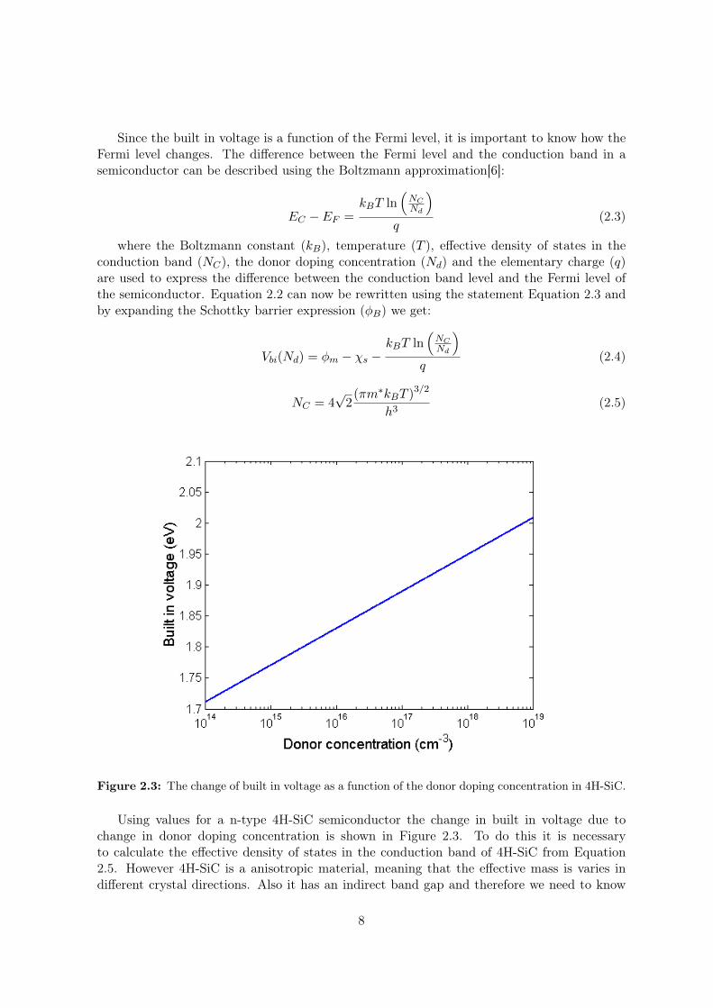
However for the metal semiconductor interface, depending on the magnitude of the workfunction of the metal (φm) and the electron affinity of the semiconductor (χs), an ohmic ora Schottky contact can be formed. The metal work function is the energy difference betweenthe vacuum level (Evac) and the Fermi level of the metal (EF ). For the electron affinityof a semiconductor the definition is the difference between the vacuum energy level and theconduction band energy level (EC) of the semiconductor. In an ideal case the transitionforms a Schottky barrier when the electron affinity of the semiconductor is smaller than thework function of the metal. Figure 2.1 shows the important properties of the materials. Thedifference between the conduction band of the semiconductor and the Fermi level of the metalthat determines the height of the Schottky barrier (φB = φm − χs), when vacuum levels ofthe semiconductor and the metal are aligned. In Figure 2.2 one can also see how the built involtage (Vbi) is formed by the band bending due to alignment of the Fermi levels. The builtin voltage can be written as:
Vbi = φB − (EC − EF ) (2.2)
6
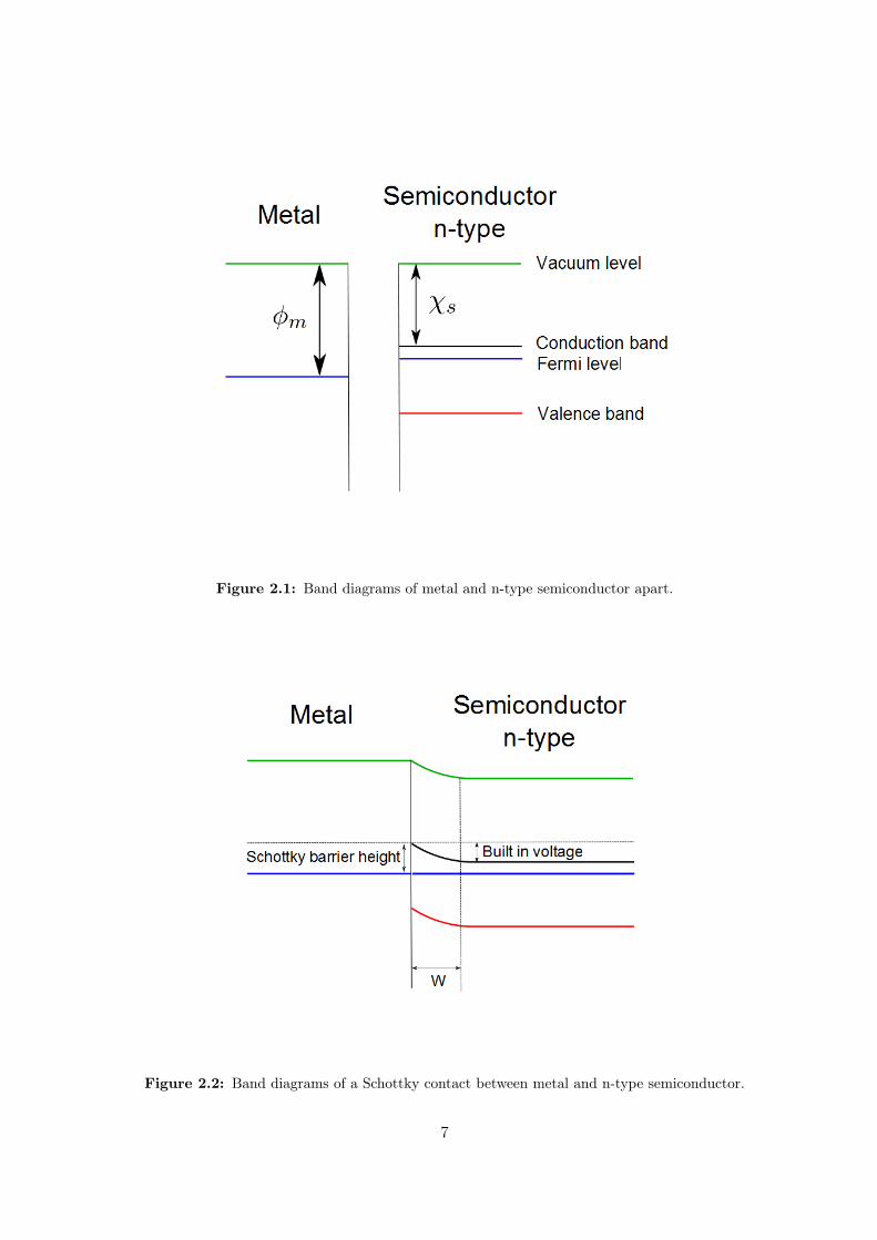
Figure 2.1: Band diagrams of metal and n-type semiconductor apart.
Figure 2.2: Band diagrams of a Schottky contact between metal and n-type semiconductor.
7
Since the built in voltage is a function of the Fermi level, it is important to know how theFermi level changes. The difference between the Fermi level and the conduction band in asemiconductor can be described using the Boltzmann approximation[6]:
EC − EF =kBT ln
(NCNd
)q
(2.3)
where the Boltzmann constant (kB), temperature (T ), effective density of states in theconduction band (NC), the donor doping concentration (Nd) and the elementary charge (q)are used to express the difference between the conduction band level and the Fermi level ofthe semiconductor. Equation 2.2 can now be rewritten using the statement Equation 2.3 andby expanding the Schottky barrier expression (φB) we get:
Vbi(Nd) = φm − χs −kBT ln
(NCNd
)q
(2.4)
NC = 4√2(πm∗kBT )
3/2
h3(2.5)
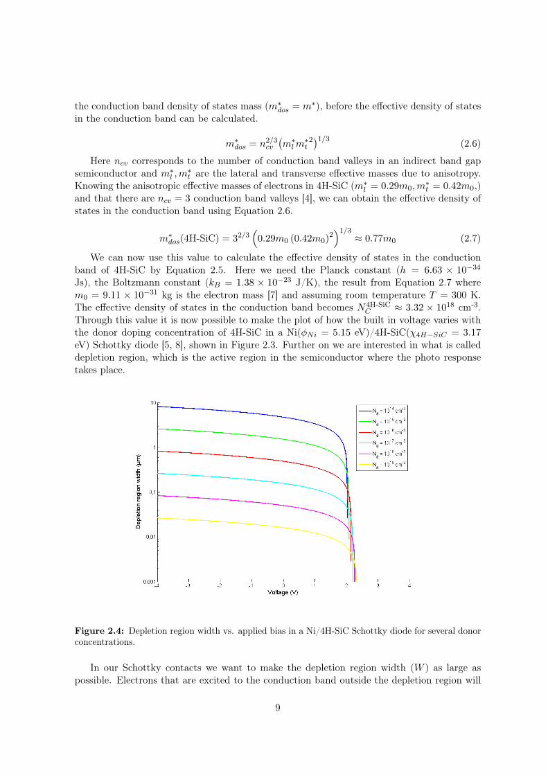
Figure 2.3: The change of built in voltage as a function of the donor doping concentration in 4H-SiC.
Using values for a n-type 4H-SiC semiconductor the change in built in voltage due tochange in donor doping concentration is shown in Figure 2.3. To do this it is necessaryto calculate the effective density of states in the conduction band of 4H-SiC from Equation2.5. However 4H-SiC is a anisotropic material, meaning that the effective mass is varies indifferent crystal directions. Also it has an indirect band gap and therefore we need to know
8
the conduction band density of states mass (m∗dos = m∗), before the effective density of states
in the conduction band can be calculated.
m∗dos = n2/3cv
(m∗
lm∗t2)1/3 (2.6)
Here ncv corresponds to the number of conduction band valleys in an indirect band gapsemiconductor and m∗
l ,m∗t are the lateral and transverse effective masses due to anisotropy.
Knowing the anisotropic effective masses of electrons in 4H-SiC (m∗l = 0.29m0,m
∗t = 0.42m0,)
and that there are ncv = 3 conduction band valleys [4], we can obtain the effective density ofstates in the conduction band using Equation 2.6.
m∗dos(4H-SiC) = 32/3
(0.29m0 (0.42m0)
2)1/3
≈ 0.77m0 (2.7)
We can now use this value to calculate the effective density of states in the conductionband of 4H-SiC by Equation 2.5. Here we need the Planck constant (h = 6.63 × 10⁻³⁴
Js), the Boltzmann constant (kB = 1.38 × 10⁻²³ J/K), the result from Equation 2.7 wherem0 = 9.11 × 10⁻³¹ kg is the electron mass [7] and assuming room temperature T = 300 K.The effective density of states in the conduction band becomes N4H-SiC
C ≈ 3.32 × 1018 cm-3.Through this value it is now possible to make the plot of how the built in voltage varies withthe donor doping concentration of 4H-SiC in a Ni(φNi = 5.15 eV)/4H-SiC(χ4H−SiC = 3.17eV) Schottky diode [5, 8], shown in Figure 2.3. Further on we are interested in what is calleddepletion region, which is the active region in the semiconductor where the photo responsetakes place.
Figure 2.4: Depletion region width vs. applied bias in a Ni/4H-SiC Schottky diode for several donorconcentrations.
In our Schottky contacts we want to make the depletion region width (W ) as large aspossible. Electrons that are excited to the conduction band outside the depletion region will
9

not make it to the electrode before they are recombined in the semiconductor. The electronsexcited to the conduction band within the depletion region can however make it to the electrodebefore recombination in the semiconductor and in this case we have photodetection. Figure2.4 shows how the depletion region width changes with different doping concentration andapplied bias (Vapp). This relation is described by Equation 2.8 [6].
W =
√2εrε0q
(Vbi(Nd)− Vapp
)Nd
(2.8)
Here εrε0 = 10.03×8.85×10−12 Fm-1 [4] is the permittivity for 4H-SiC and Vbi(Nd)−Vappis the difference between built in voltage and applied bias as a function of the donor dopingconcentration. Increasing the depletion region width will make devices fully depleted even atlow voltages, since the ones fabricated in this project will have similar or smaller structurescompared to the depletion region at zero applied bias. For low n-doped 4H-SiC (Nd = 1014
cm-3), with q = 1.60 × 10⁻¹⁹ C and no applied bias, the depletion region width becomesW ≈ 4.74 mm.
2.2.2 MSM Junction as Photo Detector
Now we know the characteristics of a metal-semiconductor junction, so let us have a look atthe metal-semiconductor-metal (MSM) junction as a photodetector. In Figure 2.5 the basicprinciple is explained. The tilt of the model illustrates the downslope created from appliedbias. To actually detect light we need the presence of photons with higher energy than theband gap. If that is the case and the energy is absorbed by an electron, it is allowed totravel through the conduction band of the semiconductor. Now the distance to the counterelectrode and the life time of the conduction band electron play a role if it will get to thecounter electrode before recombination in the semiconductor. If the carrier makes it to thecounter electrode it can be measured as a current and therefore we have a photoresponse.Here we can also define the so called quantum efficiency which is the ratio of input effect fromphotons, divided by the electrical output effect. Ideal is of course 100 %, which means thatall the present photon energy is transformed in to electrical energy.
However, if there are no photons with enough energy to emit electrons into the conductionband, there will still be a weak current passing through the junction. This current is calleddark current and mainly from thermal excitation of electrons which is the origin of the noisecurrent. The ratio between photo- and dark current is important in order to get a good signalto noise ratio of the device.
10
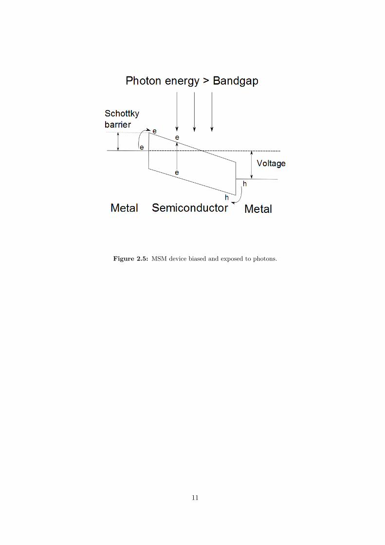
Figure 2.5: MSM device biased and exposed to photons.
11
Chapter 3
Lithography Techniques
The most common patterning technique for fabrication of micro scale devices today is pho-tolithography. But since device density is increasing to get more and more devices in a smallarea, devices need to shrink. Today’s most advanced deep UV step lithography techniquesproduce high performance processors with line widths down to 32 nm [9], but there are manyspeculations about how far down optical lithography can reach. For next generation lithog-raphy there are several candidates such as electron beam lithography, X-ray lithography andNIL. However the outlook for electron beam lithography seems to be poor since patterns arecreated by a single beam of electrons, making the process very time consuming and expensivein large scale fabrication. But if a single master pattern is fabricated it can be replicated bythe NIL technique, which is more promising for large scale fabrication. Here line widths downto 5 nm have been demonstrated [10], while it is a simple way to transfer the pattern bothcheap and fast.
This chapter will go through the two lithography techniques used in this project, pho-tolithography and NIL with focus on the latter.
3.1 Photolithography
This technique is widely used for almost all nano- and microelectronic fabrication these days,due to its simplicity and high throughput. The main principle is to expose a wafer preparedwith photoresist to UV light through a photomask. Compared to a photography the resultwill be binary in terms of exposed or non-exposed regions. If the resist is positive exposedregions are soluble in a developer while non-exposed regions remain. As the name suggests anegative resist have the opposite behavior. When the mask pattern is transfered to the resistfurther etching can be done in order to transfer pattern to substrate.
The limitations of this technique is mainly the wavelength used to expose the resist, dueto diffraction patterns. Basically it is hard to produce higher resolution than the wavelengthused for exposure. Therefore it is suggested to use as short wavelength as possible, whyphotolithography mainly is performed in the UV region. In this project a so lift-off processhas been used to fabricate micro scale MSM devices. This is described in further detail inChapter 4 Fabrication of Micro Scale Devices.
12
3.2 Nano Imprint Lithography
3.2.1 Principles of NIL
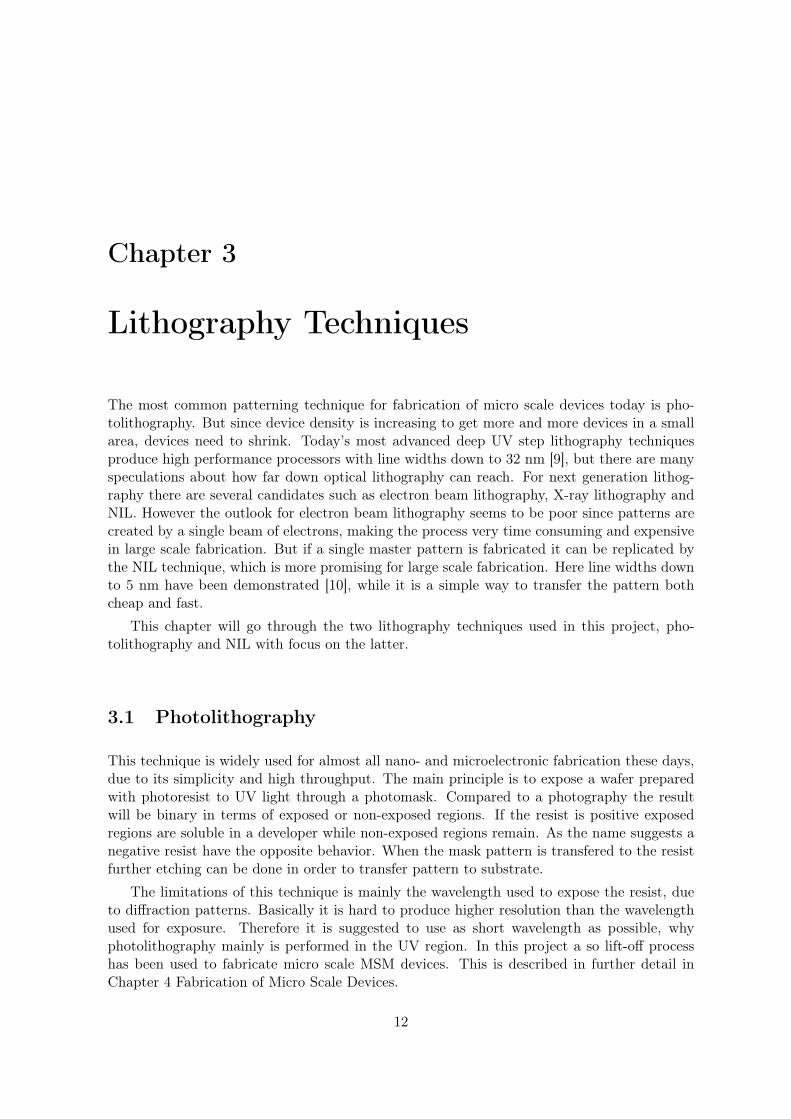
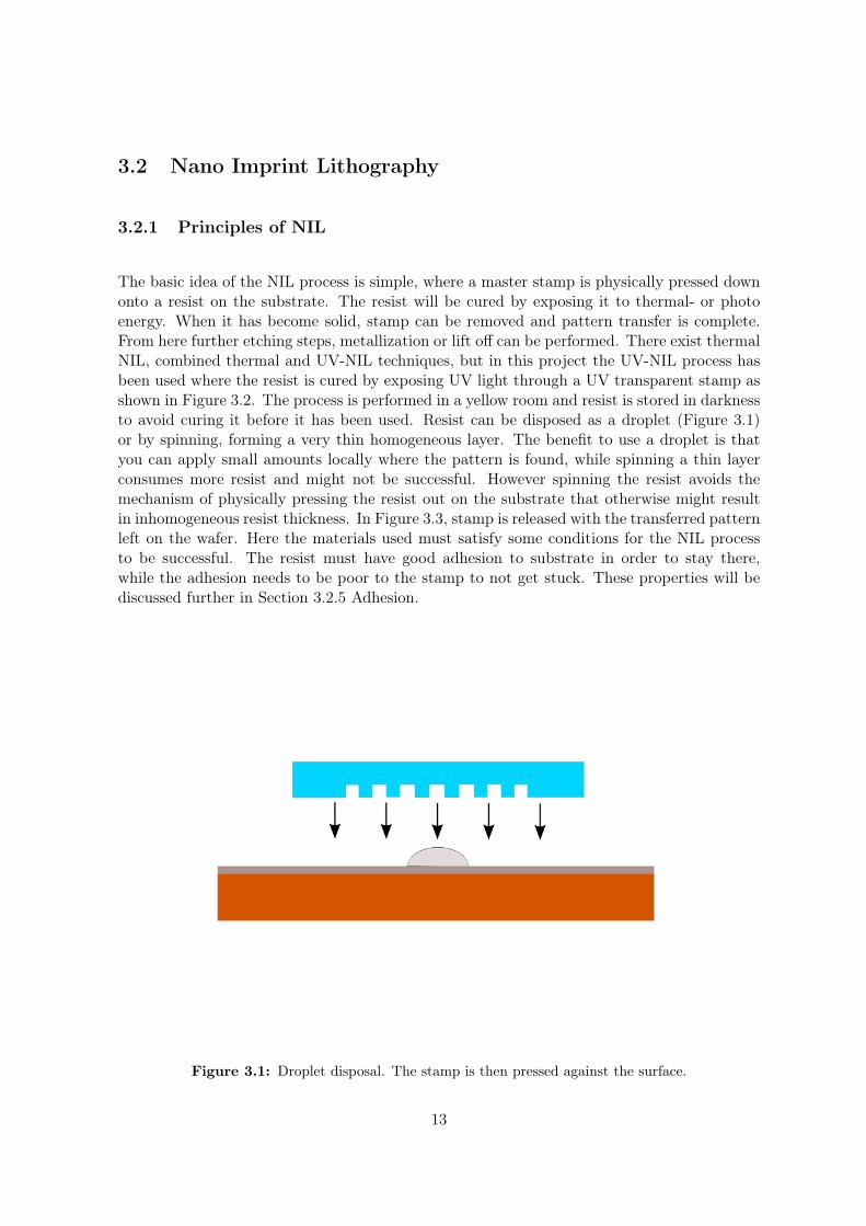
The basic idea of the NIL process is simple, where a master stamp is physically pressed downonto a resist on the substrate. The resist will be cured by exposing it to thermal- or photoenergy. When it has become solid, stamp can be removed and pattern transfer is complete.From here further etching steps, metallization or lift off can be performed. There exist thermalNIL, combined thermal and UV-NIL techniques, but in this project the UV-NIL process hasbeen used where the resist is cured by exposing UV light through a UV transparent stamp asshown in Figure 3.2. The process is performed in a yellow room and resist is stored in darknessto avoid curing it before it has been used. Resist can be disposed as a droplet (Figure 3.1)or by spinning, forming a very thin homogeneous layer. The benefit to use a droplet is thatyou can apply small amounts locally where the pattern is found, while spinning a thin layerconsumes more resist and might not be successful. However spinning the resist avoids themechanism of physically pressing the resist out on the substrate that otherwise might resultin inhomogeneous resist thickness. In Figure 3.3, stamp is released with the transferred patternleft on the wafer. Here the materials used must satisfy some conditions for the NIL processto be successful. The resist must have good adhesion to substrate in order to stay there,while the adhesion needs to be poor to the stamp to not get stuck. These properties will bediscussed further in Section 3.2.5 Adhesion.
Figure 3.1: Droplet disposal. The stamp is then pressed against the surface.
13
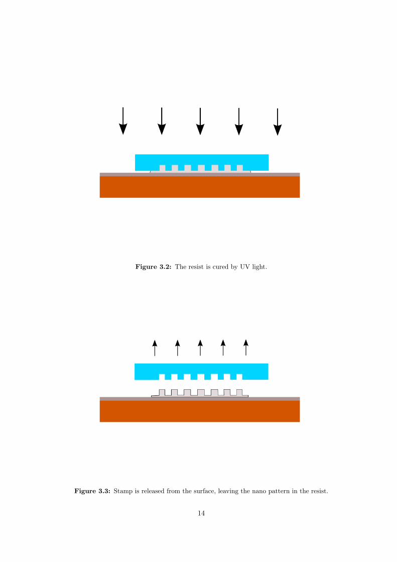
Figure 3.2: The resist is cured by UV light.
Figure 3.3: Stamp is released from the surface, leaving the nano pattern in the resist.
14
3.2.2 NIL Stamp Fabrication by e-beam Lithography
To be able to fabricate the small nano patterns in a NIL stamp you can no longer use ordinaryphotolithography. This is beyond its limits since it is very hard to make smaller structures thanthe wavelength used. However there exists lithography techniques that can reach the nanoscale such as e-beam lithography. The E-beam lithography technique can fabricate patternsbelow 15 nm, but the problem with this method the low throughput. Fabrication is made byevaporating resist with a single electron beam by scanning it through the targeted pattern.For wafer scale production this would be impossible in long term since this is way to timeconsuming for making a profit. But if a single wafer is produced with e-beam lithography thepattern can be replicated with the NIL technique, which is much faster and cheaper. BasicallyNIL share the same physical limits as e-beam lithography. Since NIL stamps are dependenton e-beam lithography, they are expensive to fabricate. But on the other hand the stamp canbe used thousands of times without having any larger defects.
3.2.3 Stamp Replication by NIL
Making a backup of a master stamp is a very good idea since they are is expensive and timeconsuming to fabricate. The loss of a master stamp because of disappearing or by damage couldbe devastating. Instead of making many stamps of the same type with e-beam lithographythey can be copied by the NIL technique. Replicating stamps this way is rather simple andjust like backing up critical data on a computer hard drive, the master stamp is not criticalanymore if broken or lost.
To fabricate a copy you first need to make an imprint with the master stamp to createa mirror image. This mirrored pattern can either be used as a negative stamp for lift-offprocesses, or like in this case to make another imprint to create the copy of the master stamp.Since the pattern has been inverted twice in this process it should look the same as the masterstamp.
3.2.4 UV Curable Nano Imprint Resists
There are a few ways to turn a liquid resist into a solidified polymer. The two common methodsusing NIL are UV exposure, thermal baking or a combination of both. In this project two typesof UV curable resists have been worked with, PAK-01 and mrCur21. PAK-01 is fabricated bythe Japanese company "TOYO GOSEI" and has been used in previous projects at Acreo as anano imprint resist. Disposal is made by droplet or spinning. The polymer itself contains Siand makes it hard to etch. A pure oxygen plasma is not enough to etch the polymer, howevera mixture of oxygen and SF6 has proven to work fine in previous NIL projects.
mrCur21 is another UV curable polymer that was investigated in this project. It is manu-factured by the German company "micro resist technology GmbH". It does not contain Si likePAK-01 and is therefore easier to etch. However the mixture of oxygen and SF6 was preferredduring this project even though the etching rate is very fast. Disposal is done by droplet orspinning. Detailed user instructions are included and it can be mixed with a thinner to createa 100 nm thin layer by spinning.
15
3.2.5 Adhesion
When the stamp is removed from the cured resist, the patterned NIL resist should stay onthe substrate. If the adhesive force to the stamp is larger than that to the substrate, thepatterned nano features cannot be transferred properly. It turns out that the NIL resist maypartly stuck on the stamp side, or in worst case the stamp and the substrate could not beseparated. In such case, the stamp has to be cleaned, and this step is rather time consuming.The adhesive force on the stamp or substrate is govern by surface energy between the stamp(or substrate) and the NIL resist. High surface energy provides a hydrophilic surface and havebetter adhesion, in contrary a lower surface energy causes hydrophobic surface and results inless adhesion. In this work the substrates surface energy was modified by applying adhesivepromoting layer to ensure good contact of patterned nanostructures on the substrate after theNIL process. To form a hydrophobic surface on the stamp side an anti sticking layer (ASL)was utilized to solve the potential problem of NIL resist remaining on the stamp.
Anti Sticking Layer
The ASL that is applied to the stamp surface is very thin, just a mono layer of the moleculeused. it is recommended to use some sort of fluorocarbon since these chemicals tend to havevery low friction and almost no materials get stuck to them. One example of fluorocarbon isTEFLON which is commercially found in almost every frying pan nowadays. A chemical calledtrichloro(1H, 1H, 2H, 2H-perfluorooctyl)silane (C8H4Cl3F13Si) was investigated since the resistprovider "micro resist technology GmbH" recommends it as a anti sticking agent. Howeverthis chemical was not tested enough to be in the fabrication process. Instead another antisticking agent that have similar properties which is called chlorotrimethylsilane (C3H9ClSi)was used. It has been used in earlier NIL projects successfully at Acreo [1] and that is themain reason it was used in this work as well.
To apply the chemical, the stamp and the chemical needs to be in an oxygen free at-mosphere since chlorotrimethylsilane is very flammable and a strong oxidizer. The stamp isloaded into a wafer box, a bit larger than the stamp itself, with about 5-6 drops from a pipettearound it inside the box. Now the wafer box should be sealed for 10 minutes. The drops ofthe chemical will be evaporated. Its vapors will grow a monolayer on all surfaces inside thebox, including the stamp.
Adhesion Promoter
To ensure a good contact between the resist and the substrate, resist providers recommendthat an adhesion promoter should be used. This layer should be as thin as possible sinceadditional materials makes etching processes more complicated. In this project a chemicalcalled mr-APS1 from micro resist technology was investigated. The substrate is coated withspin coating at 5000 rpm for 60 seconds and then baked at 150 degrees Celsius for another60 seconds. A 20 nm thick layer of adhesive promoter will remain on the surface ready touse. However the adhesion promoter was never needed for the fabrication in this project, thecontact between substrate and resist was good enough. Cleaning of substrates by acetone,2-propanol and a quick O2 plasma cleaning etch step was performed. No further pretreatmentwas necessary.
16
Chapter 4
Fabrication of Micro Scale Devices
As described in Section 1.2 Extended Work, micro scale devices were fabricated to be able tocompare performance when going to nano scale. To investigate the performance of micro scaledevices more detailed device properties can also be obtained, in this case comparison betweendifferent SiC polytypes with different finger spacing and finger widths of the MSM devices.
The fabrication process of the micro scale devices has been designed together with experi-enced personnel in the SiC research field at Acreo. It describes how the process is done afterepitaxial growth step. Therefore it will be given that before this process is performed, thesubstrates already have their designed epilayers. Chapter 4 covers fabrication and design ofthe micro scale MSM photodetectors.
4.1 Fabrication Process
4.1.1 Cleaning
Before any fabrication process is made on the substrates they need proper cleaning. A bathin 5 % HF for 5 minutes will dissolve most of the contaminations on the substrate surfacewhich might have got stuck there after the epitaxial growth. Rinse with DI-water and nitrogenblow dry follows. This should be performed immediately before next step in the process tominimize further possible contaminations.
4.1.2 Anti Reflective Coating
First a thin layer of silicon dioxide (SiO2) will be applied in the fabrication process. This hastwo purposes. Since SiO2 is an insulator the layer will prevent leaky currents on the surfacein the final devices, for example due to contaminations. Also, we will design the thickness (d)of this layer is calculated to fit constructive interference for a specific wavelength, λ = 365nm. This will increase the intensity and minimize reflection of the light in this wavelengthregion [11]. The specific wavelength has been chosen since our UV-LED used to carry outphotoresponse measurements has its peak intensity at 365 nm. The result from this antireflective coating should be a stronger signal for a certain amount of illuminated light, givingthe detector a higher sensitivity. To optimize the thickness of this layer we use the followingequation that describes constructive interference for such layer:
4dn cos θ = mλ (4.1)
17
For SiO2 the refractive index is n = 1.6 [12] and if the incident angle of incoming light θto the device is assumed to be close to zero. Here we also focus on the first order interferencem = 1 since we just want to increase one specific wavelength. Using these values we get:
d =λ
4n= 57 nm (4.2)
The SiO2 layer is grown on top of the SiC epitaxial layers by CVD and characterized bylight interferometry to determine that the target thickness has been reached.
Figure 4.1: SiC substrate with epilayers and SiO2.
4.1.3 Photolithography Patterning
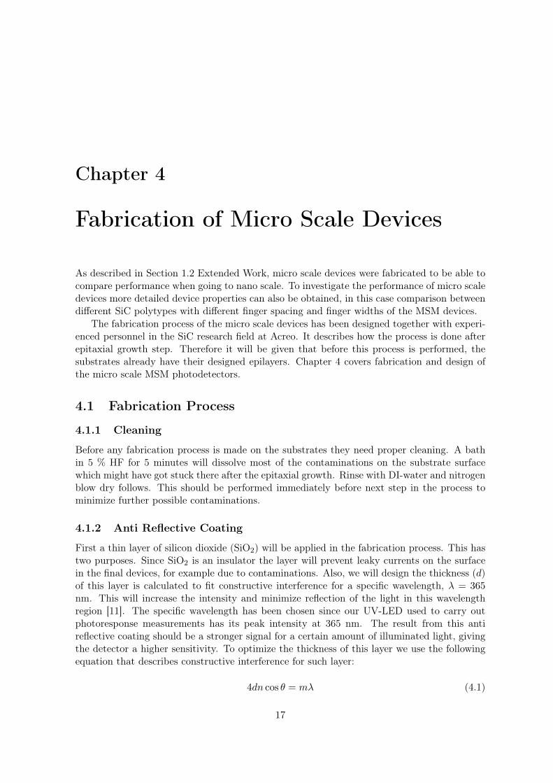
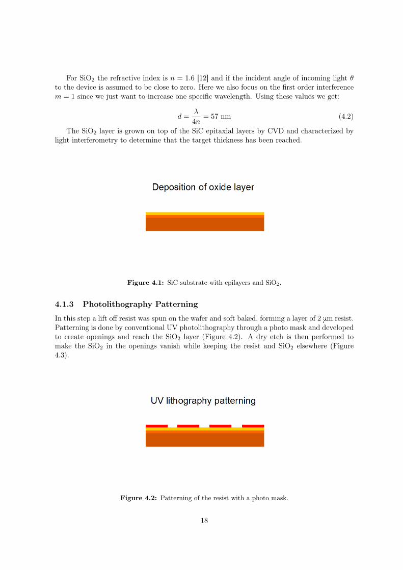
In this step a lift off resist was spun on the wafer and soft baked, forming a layer of 2 mm resist.Patterning is done by conventional UV photolithography through a photo mask and developedto create openings and reach the SiO2 layer (Figure 4.2). A dry etch is then performed tomake the SiO2 in the openings vanish while keeping the resist and SiO2 elsewhere (Figure4.3).
Figure 4.2: Patterning of the resist with a photo mask.
18
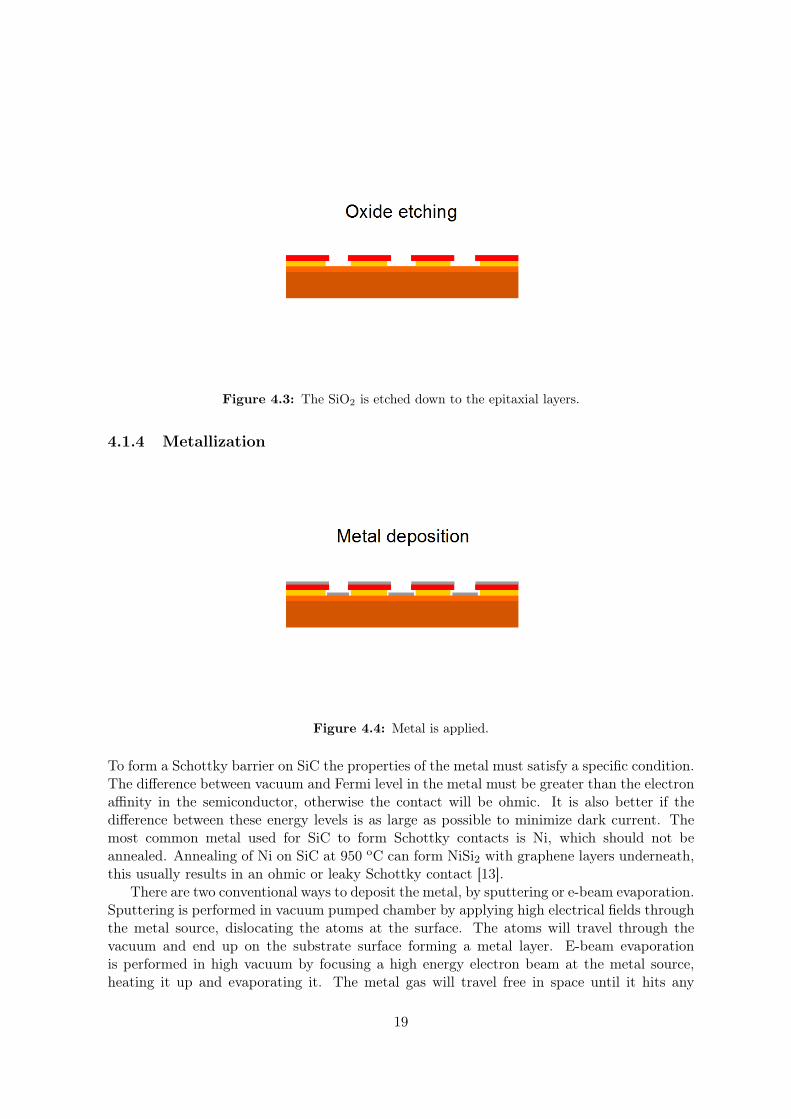
Figure 4.3: The SiO2 is etched down to the epitaxial layers.
4.1.4 Metallization
Figure 4.4: Metal is applied.
To form a Schottky barrier on SiC the properties of the metal must satisfy a specific condition.The difference between vacuum and Fermi level in the metal must be greater than the electronaffinity in the semiconductor, otherwise the contact will be ohmic. It is also better if thedifference between these energy levels is as large as possible to minimize dark current. Themost common metal used for SiC to form Schottky contacts is Ni, which should not beannealed. Annealing of Ni on SiC at 950 oC can form NiSi2 with graphene layers underneath,this usually results in an ohmic or leaky Schottky contact [13].
There are two conventional ways to deposit the metal, by sputtering or e-beam evaporation.Sputtering is performed in vacuum pumped chamber by applying high electrical fields throughthe metal source, dislocating the atoms at the surface. The atoms will travel through thevacuum and end up on the substrate surface forming a metal layer. E-beam evaporationis performed in high vacuum by focusing a high energy electron beam at the metal source,heating it up and evaporating it. The metal gas will travel free in space until it hits any
19
surface and will stick there. In this fabrication process the sputtering technique was used. Itwas thought that too high energy might damage the lift-off resist. For the 4H- and 6H SiCsamples 100 nm of Ni with 50 nm gold on top was deposited. Attempts to form Schottkycontacts on two different 3C-SiC (111) and (100) samples was also performed. Here Pt wasused as metal and the only way available to deposit it was with the e-beam evaporation tool.A 100 nm thick layer of Pt was formed on these substrates.
4.1.5 Lift-off
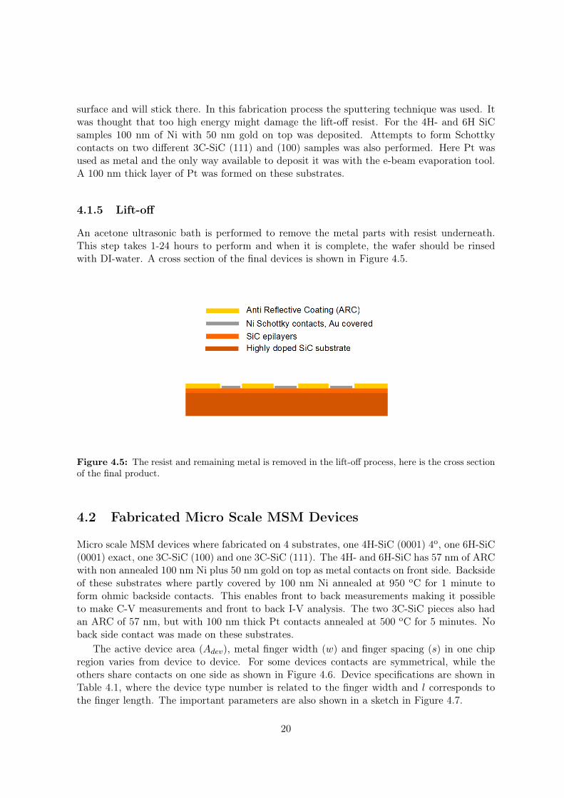
An acetone ultrasonic bath is performed to remove the metal parts with resist underneath.This step takes 1-24 hours to perform and when it is complete, the wafer should be rinsedwith DI-water. A cross section of the final devices is shown in Figure 4.5.
Figure 4.5: The resist and remaining metal is removed in the lift-off process, here is the cross sectionof the final product.
4.2 Fabricated Micro Scale MSM Devices
Micro scale MSM devices where fabricated on 4 substrates, one 4H-SiC (0001) 4o, one 6H-SiC(0001) exact, one 3C-SiC (100) and one 3C-SiC (111). The 4H- and 6H-SiC has 57 nm of ARCwith non annealed 100 nm Ni plus 50 nm gold on top as metal contacts on front side. Backsideof these substrates where partly covered by 100 nm Ni annealed at 950 oC for 1 minute toform ohmic backside contacts. This enables front to back measurements making it possibleto make C-V measurements and front to back I-V analysis. The two 3C-SiC pieces also hadan ARC of 57 nm, but with 100 nm thick Pt contacts annealed at 500 oC for 5 minutes. Noback side contact was made on these substrates.
The active device area (Adev), metal finger width (w) and finger spacing (s) in one chipregion varies from device to device. For some devices contacts are symmetrical, while theothers share contacts on one side as shown in Figure 4.6. Device specifications are shown inTable 4.1, where the device type number is related to the finger width and l corresponds tothe finger length. The important parameters are also shown in a sketch in Figure 4.7.
20
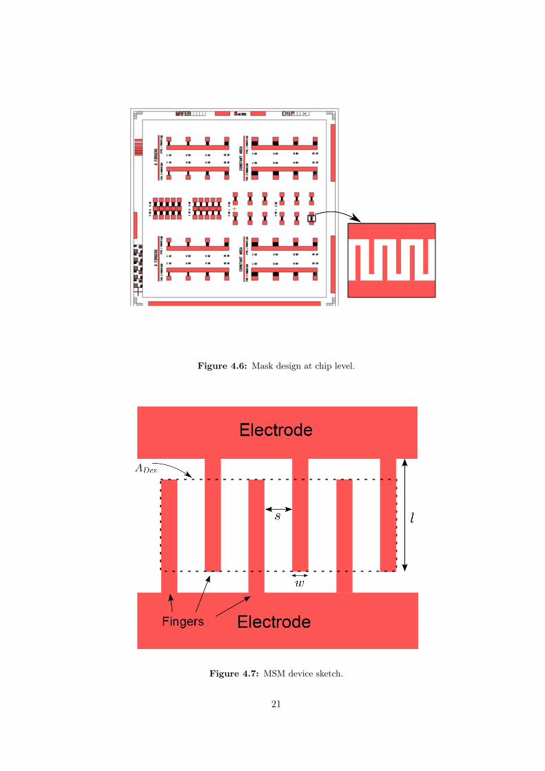
Figure 4.6: Mask design at chip level.
Figure 4.7: MSM device sketch.
21
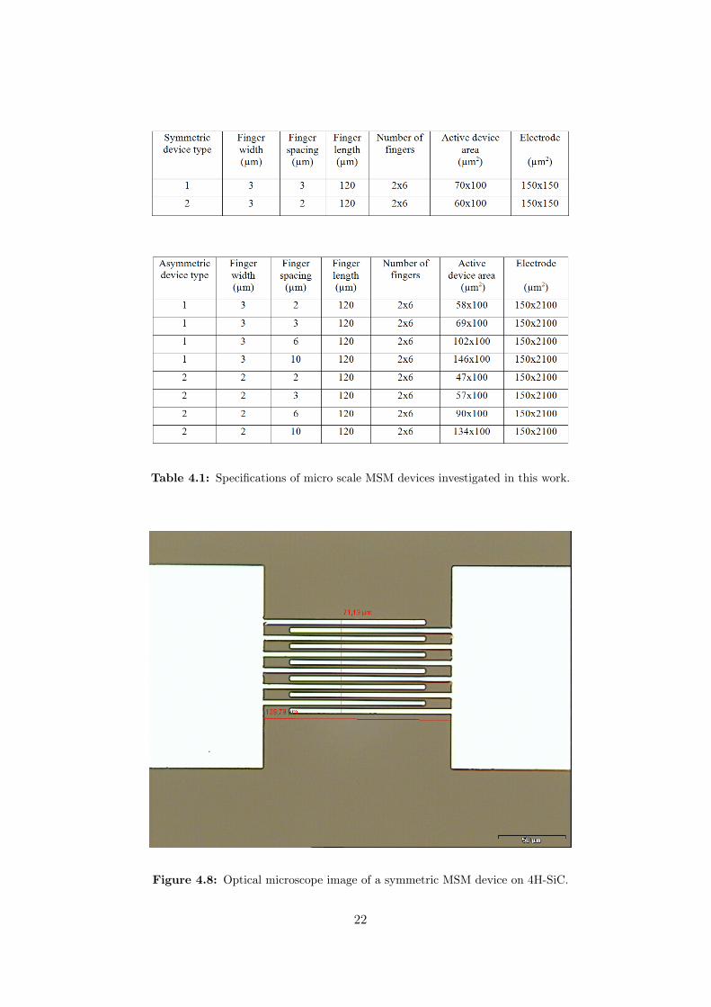
Table 4.1: Specifications of micro scale MSM devices investigated in this work.
Figure 4.8: Optical microscope image of a symmetric MSM device on 4H-SiC.
22

Fabrication for all 4 pieces of SiC was successful and most devices were visually well defined.In Figure 4.8 we can see one of the smallest features, where the finger width is 3 mm and thespacing between them is 2 mm and they are all well defined.
23
Chapter 5
Fabrication of Nano Scale Devices
The technology used to fabricate nano scale devices in this project is NIL. This chapter willcover the whole process in detail, give some insight in issues that may arise during fabrication.Device specifications and some results of fabricated devices seen through an optical microscopeare also included here.
5.1 Preparation
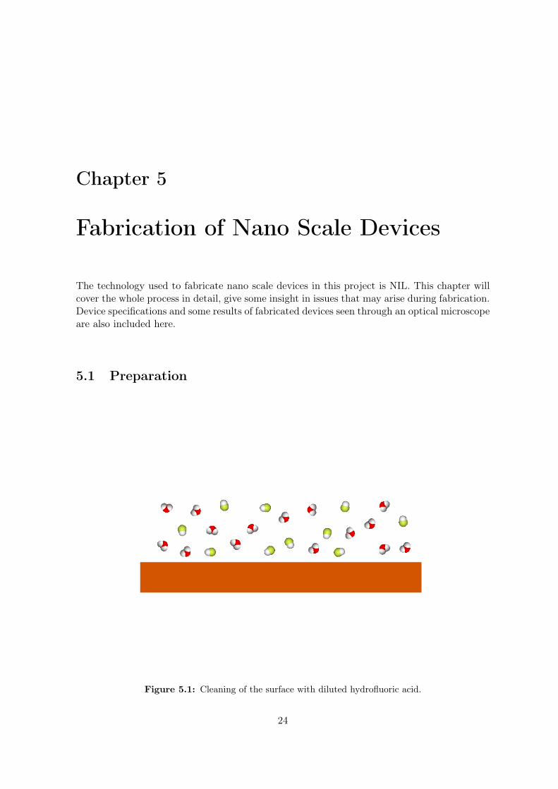
Figure 5.1: Cleaning of the surface with diluted hydrofluoric acid.
24
5.1.1 Cleaning
Just like in the micro scale fabrication process, the substrates need proper cleaning. A bathin 5 % HF for 5 minutes will dissolve most possible contaminations on the substrate surface,which might have got stuck there after epitaxial growth. This process is illustrated in Figure5.1, where a schematic cross section of the substrate and the participating molecules arevisualized. Rinse with DI-water and nitrogen blow dry follows. This should be performedimmediately before next step in the process to minimize further possible contaminations.
Here it can also be mentioned that if any of the further process steps should fail thesubstrates might need to be cleaned again. The same cleaning process just described willmake anything fabricated on top of the substrate vanish completely. Both the imprint resistand Ti that is used as metal dissolves in matters of seconds with HF treatment. This istherefore a quick and cheap process if you need to reset the work.
Figure 5.2: Map of measure points used to determine thickness after each adjustment. The blackand white region in the middle illustrates where the nano patterns of the device stamp are located.
5.1.2 Stamp Mounting
This step really needs to be prepared in advance, since it can be very time consuming. Themounting is needed because the nano imprint tool, EVG-620, which has been used is onlyconfigured for 4 inch wafers. The device stamp that has been used is a 2 inch quartz glasswafer and therefore it needs mounting on a larger wafer. As a carrier wafer a UV transparentborosilicate glass (Pyrex) wafer is used. To stick the stamp together with this carrier a UVtransparent wax is used. But before mounting of the stamp is done it needs to be cleaned andcoated with an anti sticking layer (ASL).
25
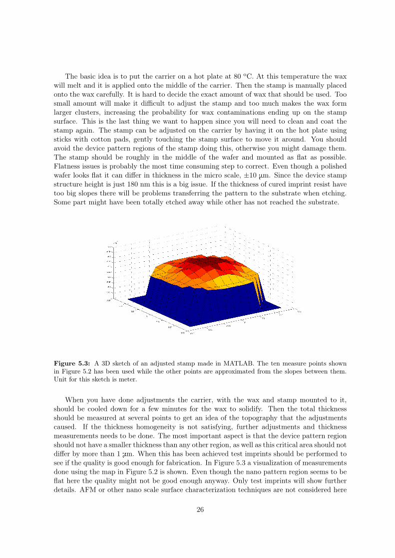
The basic idea is to put the carrier on a hot plate at 80 oC. At this temperature the waxwill melt and it is applied onto the middle of the carrier. Then the stamp is manually placedonto the wax carefully. It is hard to decide the exact amount of wax that should be used. Toosmall amount will make it difficult to adjust the stamp and too much makes the wax formlarger clusters, increasing the probability for wax contaminations ending up on the stampsurface. This is the last thing we want to happen since you will need to clean and coat thestamp again. The stamp can be adjusted on the carrier by having it on the hot plate usingsticks with cotton pads, gently touching the stamp surface to move it around. You shouldavoid the device pattern regions of the stamp doing this, otherwise you might damage them.The stamp should be roughly in the middle of the wafer and mounted as flat as possible.Flatness issues is probably the most time consuming step to correct. Even though a polishedwafer looks flat it can differ in thickness in the micro scale, ±10 mm. Since the device stampstructure height is just 180 nm this is a big issue. If the thickness of cured imprint resist havetoo big slopes there will be problems transferring the pattern to the substrate when etching.Some part might have been totally etched away while other has not reached the substrate.
Figure 5.3: A 3D sketch of an adjusted stamp made in MATLAB. The ten measure points shownin Figure 5.2 has been used while the other points are approximated from the slopes between them.Unit for this sketch is meter.
When you have done adjustments the carrier, with the wax and stamp mounted to it,should be cooled down for a few minutes for the wax to solidify. Then the total thicknessshould be measured at several points to get an idea of the topography that the adjustmentscaused. If the thickness homogeneity is not satisfying, further adjustments and thicknessmeasurements needs to be done. The most important aspect is that the device pattern regionshould not have a smaller thickness than any other region, as well as this critical area should notdiffer by more than 1 mm. When this has been achieved test imprints should be performed tosee if the quality is good enough for fabrication. In Figure 5.3 a visualization of measurementsdone using the map in Figure 5.2 is shown. Even though the nano pattern region seems to beflat here the quality might not be good enough anyway. Only test imprints will show furtherdetails. AFM or other nano scale surface characterization techniques are not considered here
26
since it would be more time consuming than a test imprint and it also might damage thepattern.
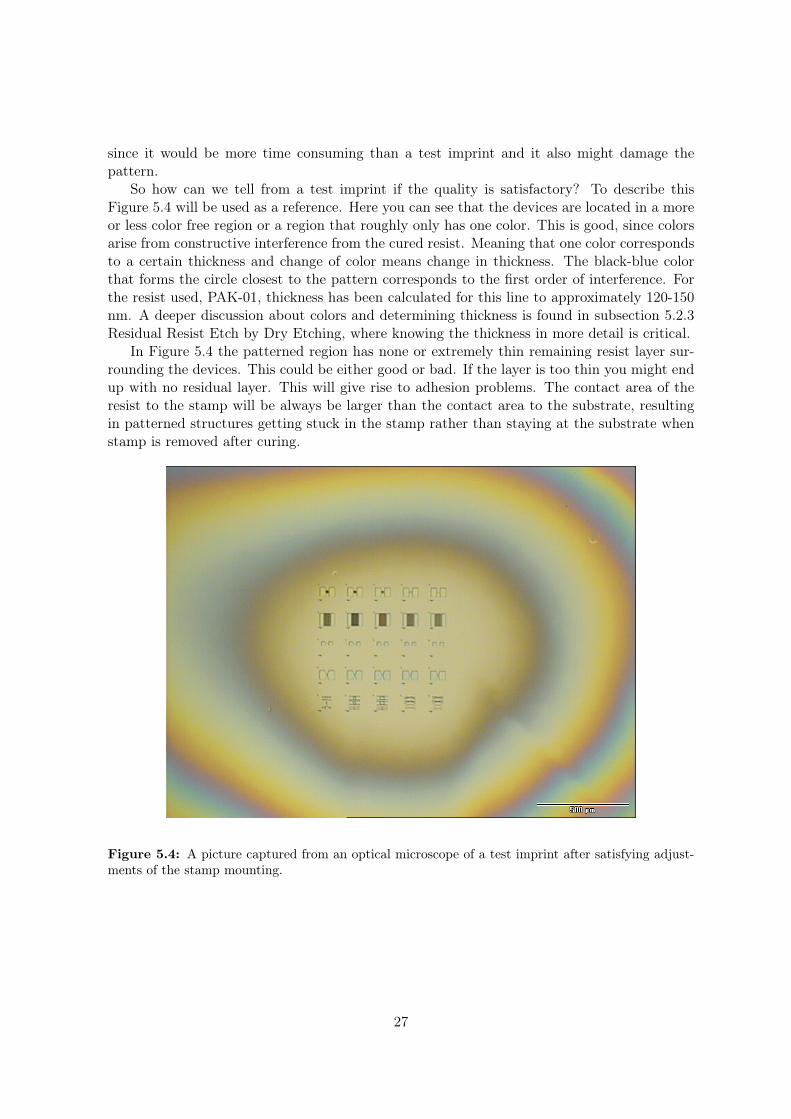
So how can we tell from a test imprint if the quality is satisfactory? To describe thisFigure 5.4 will be used as a reference. Here you can see that the devices are located in a moreor less color free region or a region that roughly only has one color. This is good, since colorsarise from constructive interference from the cured resist. Meaning that one color correspondsto a certain thickness and change of color means change in thickness. The black-blue colorthat forms the circle closest to the pattern corresponds to the first order of interference. Forthe resist used, PAK-01, thickness has been calculated for this line to approximately 120-150nm. A deeper discussion about colors and determining thickness is found in subsection 5.2.3Residual Resist Etch by Dry Etching, where knowing the thickness in more detail is critical.
In Figure 5.4 the patterned region has none or extremely thin remaining resist layer sur-rounding the devices. This could be either good or bad. If the layer is too thin you might endup with no residual layer. This will give rise to adhesion problems. The contact area of theresist to the stamp will be always be larger than the contact area to the substrate, resultingin patterned structures getting stuck in the stamp rather than staying at the substrate whenstamp is removed after curing.
Figure 5.4: A picture captured from an optical microscope of a test imprint after satisfying adjust-ments of the stamp mounting.
27
5.2 Fabrication Process
The target of this fabrication is to form top metal contacts with metal fingers by nano imprintlithography on SiC, to bring the features of the MSM photodetectors to the nano scale.Usually Ni is used as a metal with SiC for Schottky contact, since the adhesion is good andthe Schottky barrier height is rather high. However a lift off process was not possible since nosuitable stamp was available and there was no time to fabricate one either. Selective etchingwas therefore needed and that is very hard using Ni as metal. Instead Ti was used which has aslightly lower Schottky barrier height, but it has been processed in selective etches with nanoimprint at Acreo before with good results.
Active device areas will be of different types with varying metal finger width and spacing,forming rectangular and circular shapes. This will give a good base for investigating effective-ness for different geometries of the devices. The smallest features in any of these devices are50 nm.
5.2.1 Metallization
Figure 5.5: Deposition of titanium on substrate surface by e beam evaporation in a high vacuumchamber.
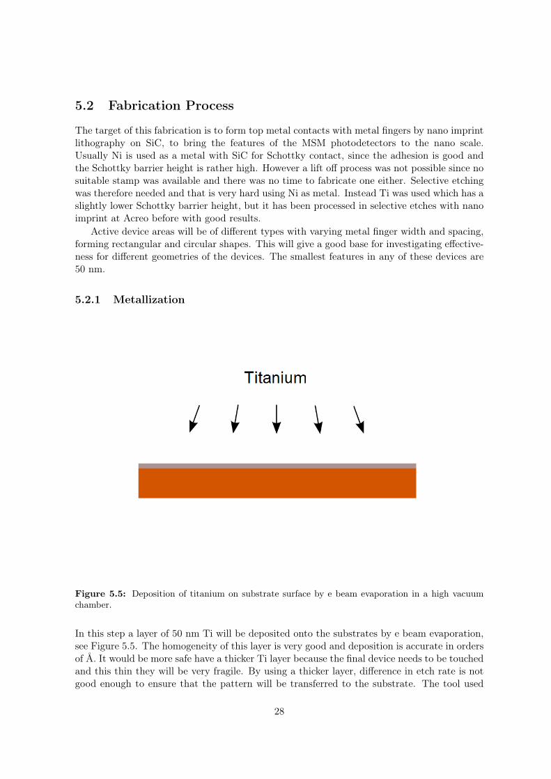
In this step a layer of 50 nm Ti will be deposited onto the substrates by e beam evaporation,see Figure 5.5. The homogeneity of this layer is very good and deposition is accurate in ordersof Å. It would be more safe have a thicker Ti layer because the final device needs to be touchedand this thin they will be very fragile. By using a thicker layer, difference in etch rate is notgood enough to ensure that the pattern will be transferred to the substrate. The tool used
28
needs to pump down to high vacuum using a cryo pump. Reaching the working pressure of5.0× 10−7 mbar takes 2 hours before process can be done.
5.2.2 Nano Imprint Lithography
Before the imprint is carried out, low energy 5 minute oxygen plasma at 150 W will beperformed. This step has proven to increase adhesion between imprint polymer and substrate.Dispense of PAK-01 is made by applying a very small drop at the substrate surface in theregion where the devices will be formed, when stamp is in contact. The size of the drop whenapplied should not be larger or smaller than 2 mm for best result. More resist will give athicker layer, perhaps too thick to transfer the pattern properly by etching. Less resist canresult in no residual layer around the pattern, which makes the cured resist to go with thestamp rather than staying on the substrate surface. Also too small amount may not fill outthe patterns.
There is no aligning needed, so the imprint is now ready to be carried out. An exposuredose of 520 mJ, which corresponds to 40 seconds in the EVG-620 nano imprint tool used, hasproven in former projects enough to cure the imprint polymer with a satisfactory result. Overexposure should not be a problem, but it can lead to different etching rates later on. Afterexposure stamp and substrate are carefully separated to avoid damaging the pattern.
5.2.3 Residual Resist Etch by Dry Etching
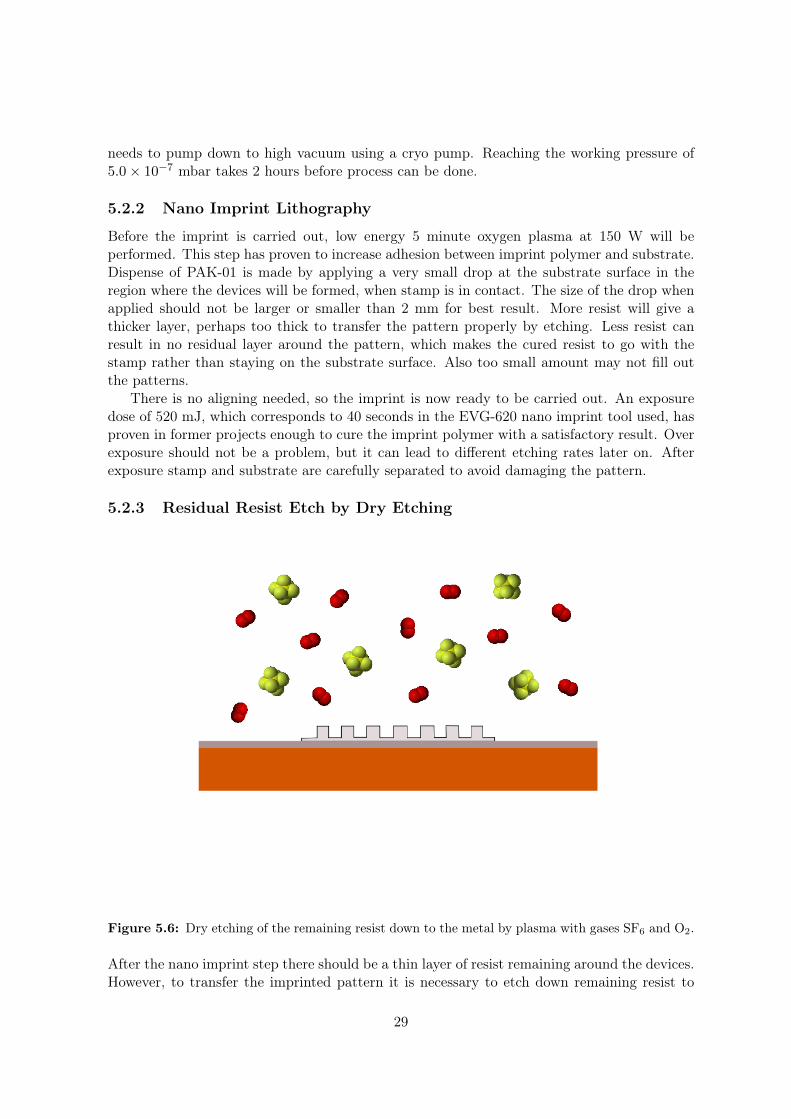
Figure 5.6: Dry etching of the remaining resist down to the metal by plasma with gases SF6 and O2.
After the nano imprint step there should be a thin layer of resist remaining around the devices.However, to transfer the imprinted pattern it is necessary to etch down remaining resist to
29
the metal. Here it is very important to know the thickness of the remaining resist and etchingrate to accurately process the sample. To measure the thickness one can use a thin filminterferometry tool. Knowing the refractive index of the cured resist n = 1.508 [14] it ispossible to examine constructive interference for wavelengths to determine thickness. Therewas no such program for the tool used though and there was no knowledge or time to investigatehow to make a new program, so a similar already existing program was used that originallydesigned to measure film thickness of SiO2 on a Si substrate. The main difference is thatthe refractive index of SiO2 is slightly higher n = 1.6, but since it is almost the same it canbe used for giving an approximation of the thickness. Looking at Equation 4.2 one can seethat the increase of the refractive index will give a smaller thickness.This is good since it willreduce the probability of over etching from calculations of etching time knowing the thicknessand etch rate. It is better to make two or more runs of etching being on the safe side, ratherthan over etching which might destroy the pattern.
5.2.4 Metal Etch
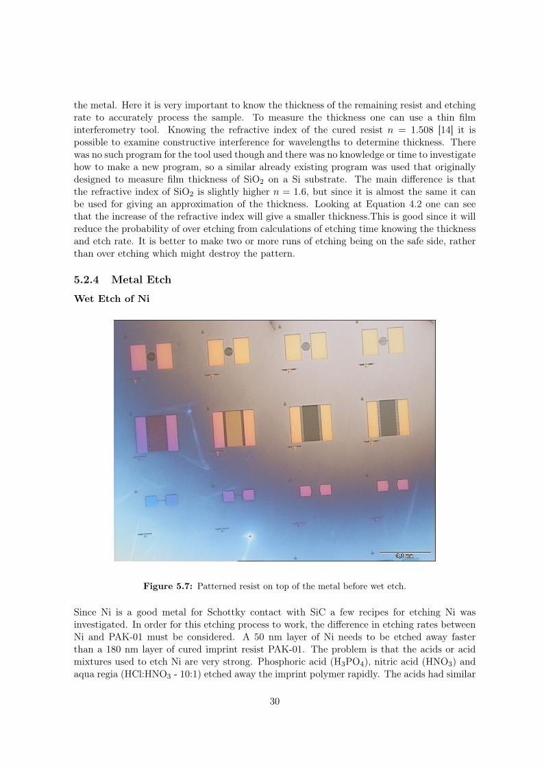
Wet Etch of Ni
Figure 5.7: Patterned resist on top of the metal before wet etch.
Since Ni is a good metal for Schottky contact with SiC a few recipes for etching Ni wasinvestigated. In order for this etching process to work, the difference in etching rates betweenNi and PAK-01 must be considered. A 50 nm layer of Ni needs to be etched away fasterthan a 180 nm layer of cured imprint resist PAK-01. The problem is that the acids or acidmixtures used to etch Ni are very strong. Phosphoric acid (H3PO4), nitric acid (HNO3) andaqua regia (HCl:HNO3 - 10:1) etched away the imprint polymer rapidly. The acids had similar
30
behavior, they lifted the resist from the surface before it was etched away making it impossibleto transfer the pattern. However a more gentle and suitable recipe was investigated consistingof a mixture of phosphoric acid, nitric acid, acetic acid and DI-water with the ratio 3:3:1:1.This mixture has a very temperature sensitive etching rate, but at 34 oC the etching rate wasfound to be around 1.1 nm/s. The etching of PAK-01 was much slower for this recipe, buteven though this was the best attempt to wet etch Ni the result is clearly that it does not suitnano scale device fabrication. Device pattern before wet etching is shown in Figure 5.7 andafter in Figure 5.8.
Figure 5.8: Remaining metal structures after wet etch.
The etching time for the device that is shown in Figure 5.8 was 45 seconds. It was theonly device that one could be recognized from the stamp pattern after this process, so theconclusion is that wet etching of Ni is not an option. Instead the metal was switched to Tiwhich has been used to fabricate similar devices on GaN in earlier project.
Dry Etch of Ti
Since no suitable recipe to etch Ni was found, Ti would have to be used instead. It hasbeen used in the same fabrication process before, also dry etching of this metal has been welloptimized. The dry etch is performed with O2, N2, BCl3 and CF4 gases with forward powerof 600 W with the P5000 tool in Electrum laboratory. Etching rate is fast so only 13 secondsis needed to etch down the metal layer to the epitaxial layers. This recipe does also etch theresist very fast but only two times as fast as the Ti. Since the Ti thickness is 50 nm and theresist thickness 180 nm, there is no harm done if the sample should be slightly over etched.
31
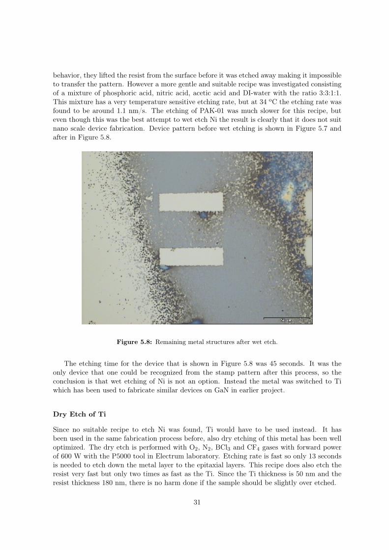
Figure 5.9: Dry selective etching of the metal down to the substrate.
5.2.5 Resist Stripping by Dry Etch
When the metal etch is complete there should be some remaining resist on the MSM devicesif not strongly over etched. This must be removed in order to measure the devices at a probestation since the imprint resist PAK-01 is insulating. To determine how thick this layer isAFM is used. It is known that the metal thickness is 50 nm, so any value that is larger in stepheight from metal finger to substrate is considered as remaining resist. When the step heightis determined the same process as in section 5.2.3 is performed, where the etch rate of PAK-01roughly is 5 nm/s. This etching process is not harmful to the Ti, so a small over etch can bedone to make sure that the resist gets stripped properly. This completes the nano fabricationprocess and the MSM devices are now ready for measurements. An optical microscope imageof final devices is shown in Figure 5.11 and a cross section model image in Figure 5.12.
32
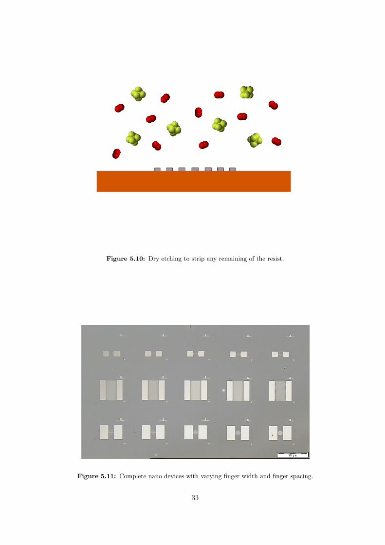
Figure 5.10: Dry etching to strip any remaining of the resist.
Figure 5.11: Complete nano devices with varying finger width and finger spacing.
33
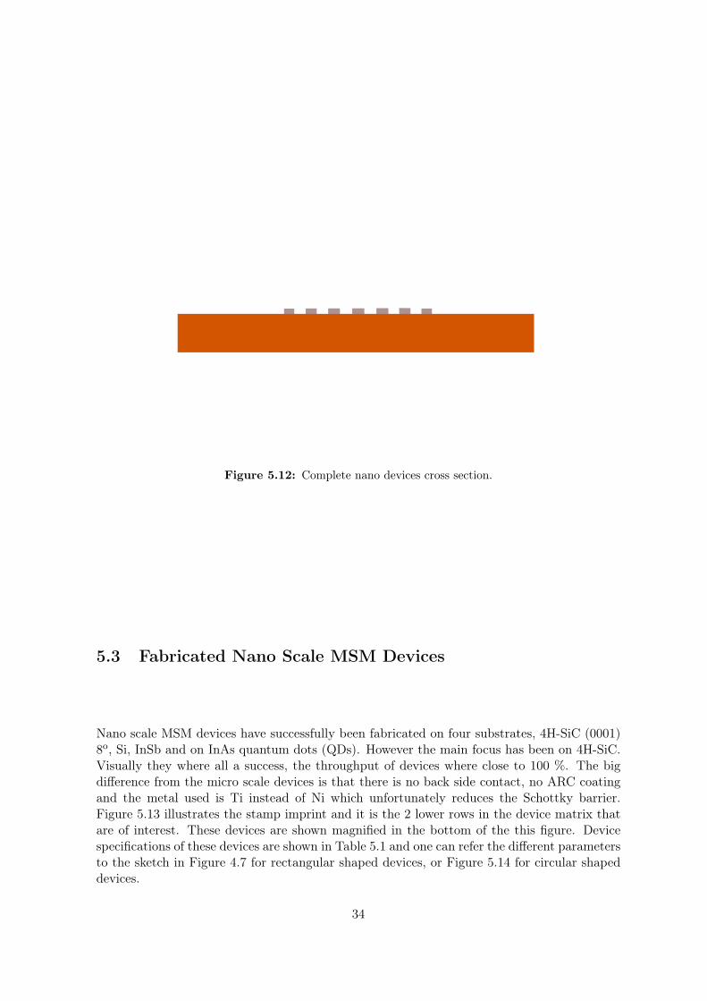
Figure 5.12: Complete nano devices cross section.
5.3 Fabricated Nano Scale MSM Devices
Nano scale MSM devices have successfully been fabricated on four substrates, 4H-SiC (0001)8o, Si, InSb and on InAs quantum dots (QDs). However the main focus has been on 4H-SiC.Visually they where all a success, the throughput of devices where close to 100 %. The bigdifference from the micro scale devices is that there is no back side contact, no ARC coatingand the metal used is Ti instead of Ni which unfortunately reduces the Schottky barrier.Figure 5.13 illustrates the stamp imprint and it is the 2 lower rows in the device matrix thatare of interest. These devices are shown magnified in the bottom of the this figure. Devicespecifications of these devices are shown in Table 5.1 and one can refer the different parametersto the sketch in Figure 4.7 for rectangular shaped devices, or Figure 5.14 for circular shapeddevices.
34
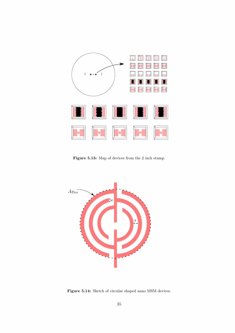
Figure 5.13: Map of devices from the 2 inch stamp.
Figure 5.14: Sketch of circular shaped nano MSM devices.
35

Table 5.1: Nano scale MSM photo detector specifications.
36
Chapter 6
Characterization of Devices
Micro scale MSM devices were fabricated on 3C- 4H- and 6H-SiC and nano scale on 4H-SiC,Si, InSb and on InAs QDs by nano imprint lithography. In this thesis report the focus of devicecharacterization will completely be on 4H-SiC and 6H-SiC. Unfortunately the MSM devices onboth 3C-SiC substrates formed ohmic instead of Schottky contacts, why these results are notdiscussed further. Si MSM nano devices have been demonstrated before, while InSb substrateand InAs QDs are for infra red wavelength detection and should be analyzed in future work.
In this chapter the characteristics of the devices are analyzed in physical, electric, opticaland electro-optical aspects.
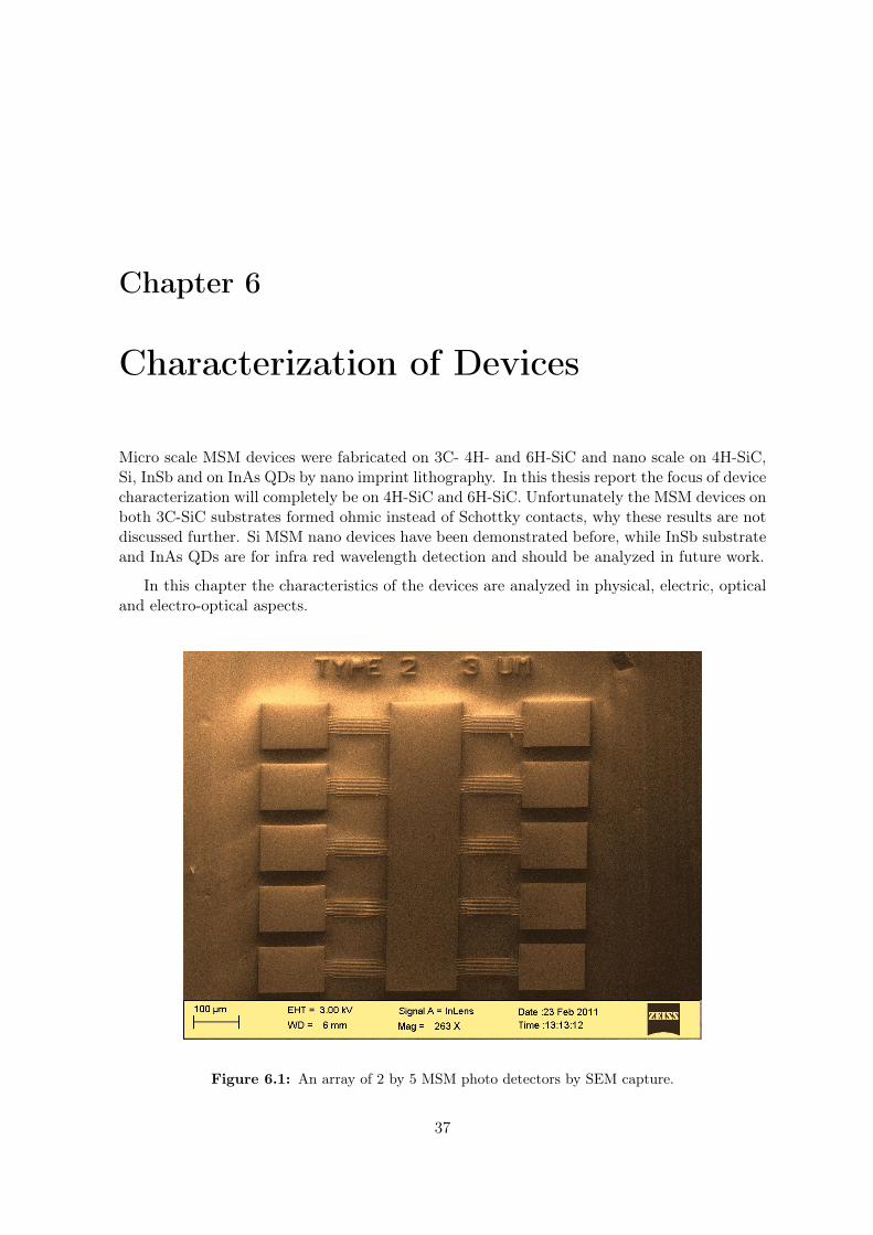
Figure 6.1: An array of 2 by 5 MSM photo detectors by SEM capture.
37
6.1 Material Characterization
To characterize the material several techniques has been used for different purposes. Opticalmicroscopes have their limits due to optical wavelengths so both SEM and AFM has beenused to analyze size of the devices. Also to determine the doping concentration and type, C-Vmeasurements have been performed.
6.1.1 Scanning Electron Microscopy
Surface characterization at nano scale is impossible to do by traditional optical microscopes,since the size of the optical wavelength is a limit (400-700 nm for the visible spectra). Howeverone can achieve higher resolution by using an electron beam as its wavelength can be muchshorter; this advantage is used in Scanning Electron Microscopy (SEM). The drawback withthis technique is that the energy density of the electron beam needs to be extremely high inorder to give resolution at nano scale. It is very likely that the exposed material might belocally evaporated where the beam is too focused. The technique is anyway rather fast andcaptures black and white images with good quality. In Figure 6.1 a SEM capture is shown ofsome of the micro scale MSM photo detectors.
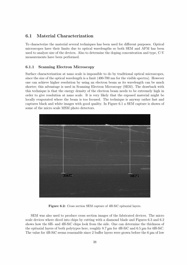
Figure 6.2: Cross section SEM capture of 4H-SiC epitaxial layers.
SEM was also used to produce cross section images of the fabricated devices. The microscale devices where diced into chips by cutting with a diamond blade and Figures 6.3 and 6.2shows how the 6H- and 4H-SiC chips look from the side. One can determine the thickness ofthe epitaxial layers of both polytypes here, roughly 8.7 mm for 4H-SiC and 6.5 mm for 6H-SiC.The value for 4H-SiC seems reasonable since 2 buffer layers were grown before the 6 mm of low
38
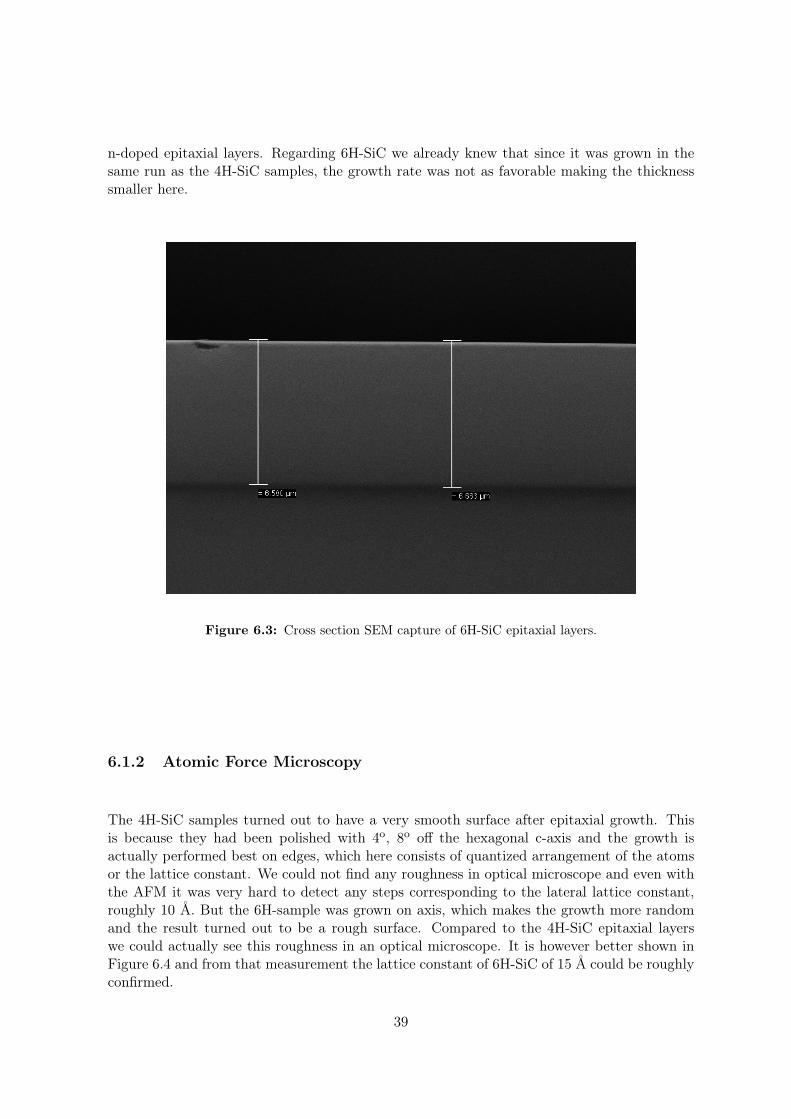
n-doped epitaxial layers. Regarding 6H-SiC we already knew that since it was grown in thesame run as the 4H-SiC samples, the growth rate was not as favorable making the thicknesssmaller here.
Figure 6.3: Cross section SEM capture of 6H-SiC epitaxial layers.
6.1.2 Atomic Force Microscopy
The 4H-SiC samples turned out to have a very smooth surface after epitaxial growth. Thisis because they had been polished with 4o, 8o off the hexagonal c-axis and the growth isactually performed best on edges, which here consists of quantized arrangement of the atomsor the lattice constant. We could not find any roughness in optical microscope and even withthe AFM it was very hard to detect any steps corresponding to the lateral lattice constant,roughly 10 Å. But the 6H-sample was grown on axis, which makes the growth more randomand the result turned out to be a rough surface. Compared to the 4H-SiC epitaxial layerswe could actually see this roughness in an optical microscope. It is however better shown inFigure 6.4 and from that measurement the lattice constant of 6H-SiC of 15 Å could be roughlyconfirmed.
39
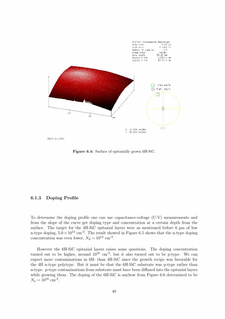
Figure 6.4: Surface of epitaxially grown 6H-SiC.
6.1.3 Doping Profile
To determine the doping profile one can use capacitance-voltage (C-V) measurements andfrom the slope of the curve get doping type and concentration at a certain depth from thesurface. The target for the 4H-SiC epitaxial layers were as mentioned before 6 mm of lown-type doping, 5.0× 1014 cm-3. The result showed in Figure 6.5 shows that the n-type dopingconcentration was even lower, Nd = 1014 cm-3.
However the 6H-SiC epitaxial layers raises some questions. The doping concentrationturned out to be higher, around 1016 cm-3, but it also turned out to be p-type. We canexpect more contaminations in 6H- than 4H-SiC since the growth recipe was favorable forthe 4H n-type polytype. But it must be that the 6H-SiC substrate was p-type rather thann-type. p-type contaminations from substrate must have been diffused into the epitaxial layerswhile growing them. The doping of the 6H-SiC is anyhow from Figure 6.6 determined to beNa = 1016 cm-3.
40
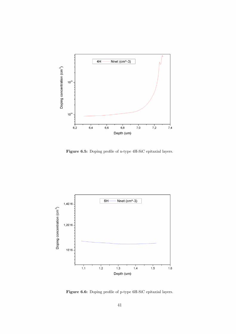
Figure 6.5: Doping profile of n-type 4H-SiC epitaxial layers.
Figure 6.6: Doping profile of p-type 6H-SiC epitaxial layers.
41
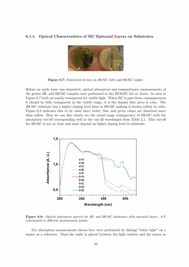
6.1.4 Optical Characteristics of SiC Epitaxial Layers on Substrates
Figure 6.7: Fabricated devices on 4H-SiC (left) and 6H-SiC (right).
Before an oxide layer was deposited, optical absorption and transmittance measurements ofthe grown 4H- and 6H-SiC samples were performed in the IMAGIC lab at Acreo. As seen inFigure 6.7 both are partly transparent for visible light. When SiC is pure from contaminationsit should be fully transparent in the visible range, it is the dopant that gives it color. The4H-SiC substrate has a higher doping level than in 6H-SiC making it brown/yellow in color.Figure 6.8 indicates this to be valid since violet, blue and green colors are absorbed morethan yellow. Here we can also clearly see the visual range transparency of 6H-SiC with theabsorption cut-off corresponding well to the cut-off wavelength from Table 2.1. This cut-offfor 4H-SiC is not as clear and must depend on higher doping level in substrate.
Figure 6.8: Optical absorption spectra for 4H- and 6H-SiC substrates with epitaxial layers. A-Fcorresponds to different measurement points.
The absorption measurements shown here were performed by shining "white light" on asensor as a reference. Then the wafer is placed between the light emitter and the sensor so
42

that transmittance is measured. Absorption is here defined as light that does not transmitthrough the material, so any reflection is neglected as absorption. Also it is worth mentioningthat neither emitter or sensor are linear in response or illumination, but they still show theoptical properties well of the materials.
Attempts to determine the effectiveness of the ARC layer were also made but not success-ful. For example reflection measurements gave to weak signals compared to background noise,therefore we could not read out any information about how much reflection of the wavelength365 nm had been decreased. Transmittance measurements through the wafer made no differ-ence either from before. So there is no way from these measurements to tell how much or ifthe ARC layer improved the absorption of the wavelength 365 nm.
43
6.2 Spectral Response for Micro Scale MSM Devices
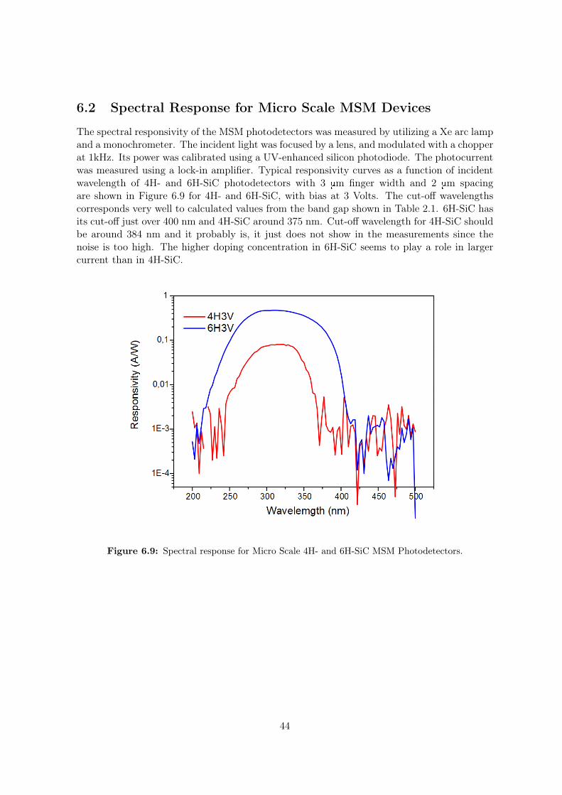
The spectral responsivity of the MSM photodetectors was measured by utilizing a Xe arc lampand a monochrometer. The incident light was focused by a lens, and modulated with a chopperat 1kHz. Its power was calibrated using a UV-enhanced silicon photodiode. The photocurrentwas measured using a lock-in amplifier. Typical responsivity curves as a function of incidentwavelength of 4H- and 6H-SiC photodetectors with 3 mm finger width and 2 mm spacingare shown in Figure 6.9 for 4H- and 6H-SiC, with bias at 3 Volts. The cut-off wavelengthscorresponds very well to calculated values from the band gap shown in Table 2.1. 6H-SiC hasits cut-off just over 400 nm and 4H-SiC around 375 nm. Cut-off wavelength for 4H-SiC shouldbe around 384 nm and it probably is, it just does not show in the measurements since thenoise is too high. The higher doping concentration in 6H-SiC seems to play a role in largercurrent than in 4H-SiC.
Figure 6.9: Spectral response for Micro Scale 4H- and 6H-SiC MSM Photodetectors.
44
6.3 Photo Response and I-V Characteristics
I-V characteristics of dark current and photocurrent have been measured in darkness andby illuminating the samples with different UV light sources respectively. Mainly UV-LEDshave been used since they gave better control, stability and higher intensity than a UV lamp.The photocurrents shown in this chapter come from illumination with a 365 nm UV-LEDwith a flux density of 0.5 mW/cm-2 at a distance of 6 cm between light source and detector.All measurements have been performed at room temperature. The electric current shown infigures in this section are the absolute value of the actual current. Of course a negative biasgives a negative current, but taking the absolute value gives a better idea of the characteristics.
6.3.1 Micro Scale Devices
As mentioned before MSM devices were fabricated on 3C- 4H- and 6H-SiC. Unfortunately theMSM on both 3C-SiC substrates formed ohmic contacts, instead of Schottky. Their resultsare therefore not discussed any further. However n-type 4H- and p-type 6H-SiC both workedsuccessfully with expected MSM I-V characteristics. It was mentioned that the photocurrentwas larger in the 6H-SiC devices compared to 4H-SiC, which is seen here. I-V characteristicswere done using a probe station with very sharp needles just touching contact pads of thedevices on the top side. A voltage sweep from negative to positive bias was done to measurethe current. Since the dark current was very low in 4H-SiC MSM devices special equipment,shielded and with signal filters had to be used to achieve the dark current. Photocurrent couldbe measured by a manual probe station since the signals were well above the noise level of thatequipment, 100 pA. The results from symmetric contact MSM devices on 4H-SiC is shownin Figure 6.10, where 5 orders of magnitude between dark current and photocurrent is seen.For example similar devices, although vertical MSM instead of horizontal, reported from anItalian group [15] showed a magnitude difference of 2 orders for the same measurements. Onthe other hand their doping concentration of SiC was higher (Nd = 2.7× 1015 cm-3), so thatcould be one reason why our devices were an improvement. Also earlier projects at Acreoconcerning GaN MSM UV detectors only showed one order of magnitude in difference. Theimprovement by using SiC should be that the material quality is higher since SiC epitaxy ismore mature than GaN, also the electron affinity of 4H-SiC (3.2 eV) is lower than in GaN (4.1eV). This material property makes it possible to have a higher Schottky barrier using 4H-SiCthan in GaN, thus reducing the noise.
45
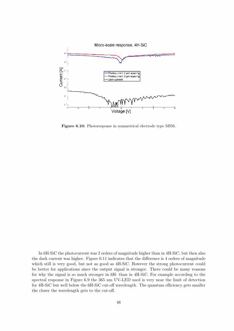
Figure 6.10: Photoresponse in symmetrical electrode type MSM.
In 6H-SiC the photocurrent was 2 orders of magnitude higher than in 4H-SiC, but then alsothe dark current was higher. Figure 6.11 indicates that the difference is 4 orders of magnitudewhich still is very good, but not as good as 4H-SiC. However the strong photocurrent couldbe better for applications since the output signal is stronger. There could be many reasonsfor why the signal is so much stronger in 6H- than in 4H-SiC. For example according to thespectral response in Figure 6.9 the 365 nm UV-LED used is very near the limit of detectionfor 4H-SiC but well below the 6H-SiC cut-off wavelength. The quantum efficiency gets smallerthe closer the wavelength gets to the cut-off.
46
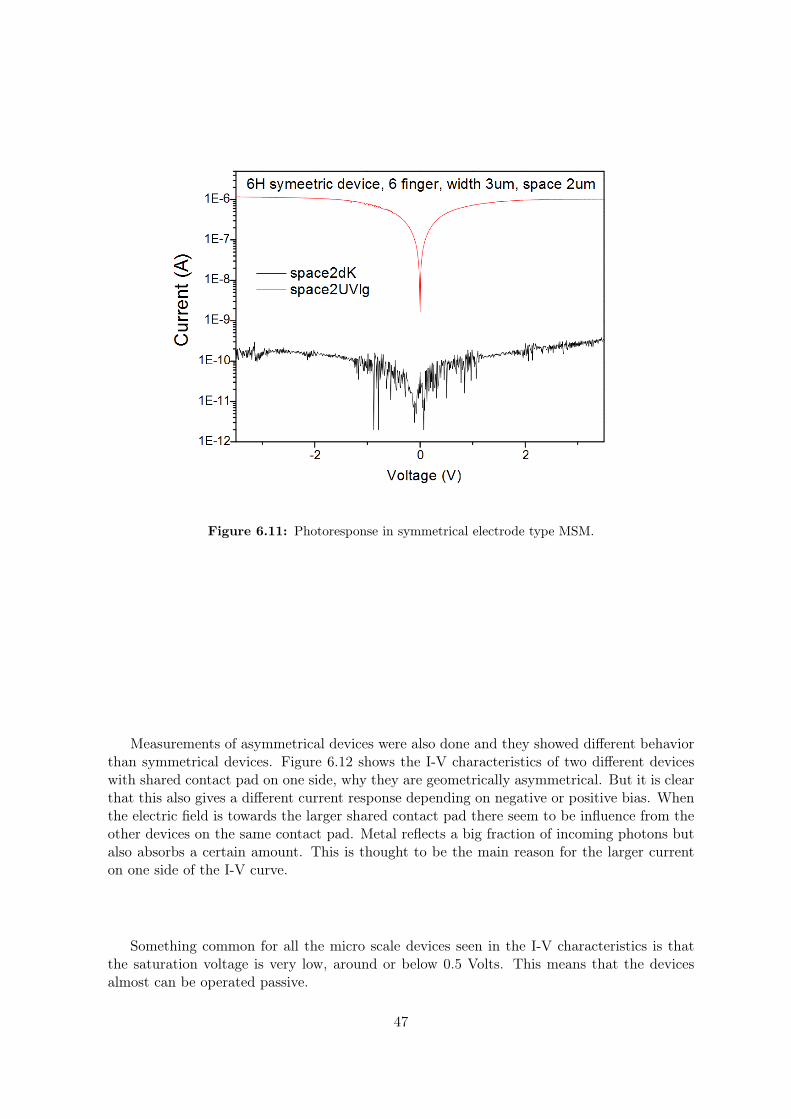
Figure 6.11: Photoresponse in symmetrical electrode type MSM.
Measurements of asymmetrical devices were also done and they showed different behaviorthan symmetrical devices. Figure 6.12 shows the I-V characteristics of two different deviceswith shared contact pad on one side, why they are geometrically asymmetrical. But it is clearthat this also gives a different current response depending on negative or positive bias. Whenthe electric field is towards the larger shared contact pad there seem to be influence from theother devices on the same contact pad. Metal reflects a big fraction of incoming photons butalso absorbs a certain amount. This is thought to be the main reason for the larger currenton one side of the I-V curve.
Something common for all the micro scale devices seen in the I-V characteristics is thatthe saturation voltage is very low, around or below 0.5 Volts. This means that the devicesalmost can be operated passive.
47
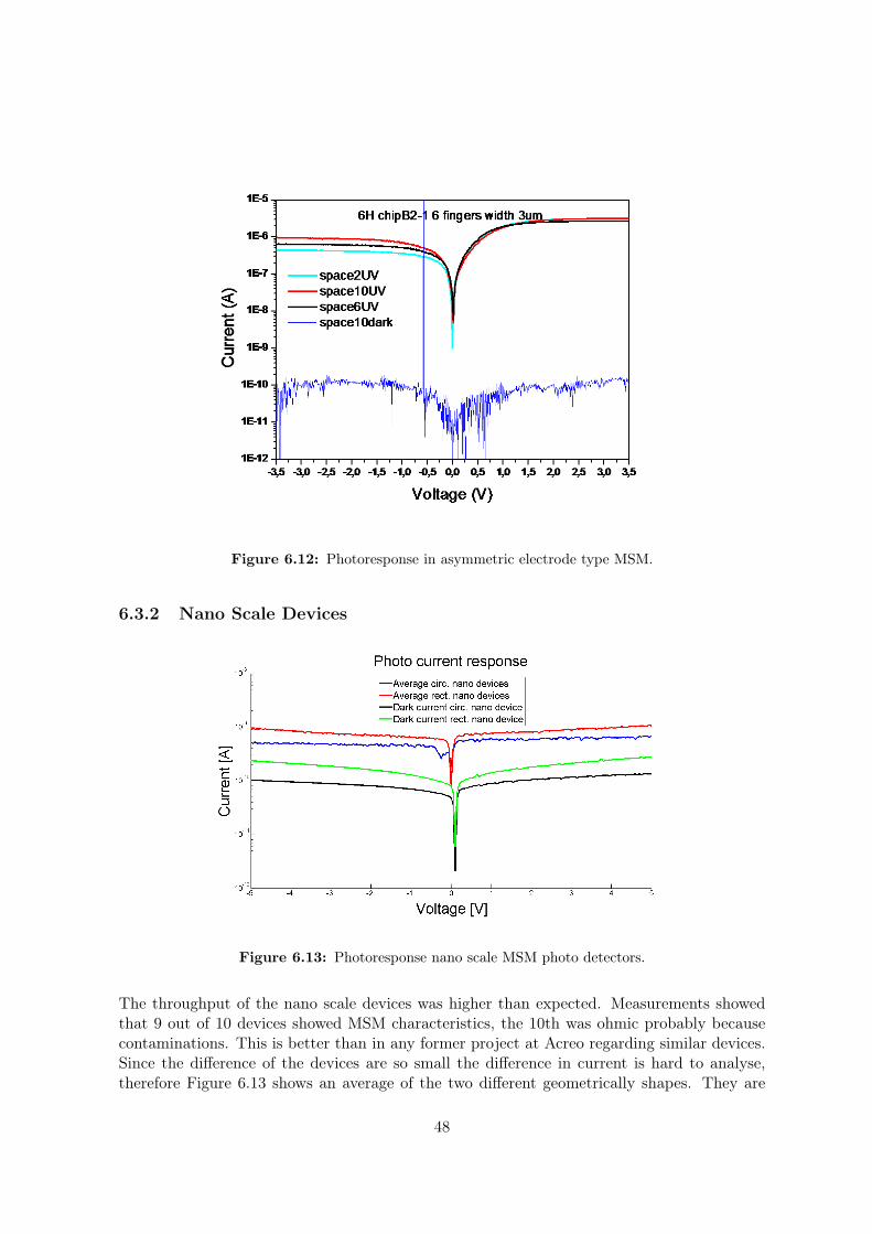
Figure 6.12: Photoresponse in asymmetric electrode type MSM.
6.3.2 Nano Scale Devices
Figure 6.13: Photoresponse nano scale MSM photo detectors.
The throughput of the nano scale devices was higher than expected. Measurements showedthat 9 out of 10 devices showed MSM characteristics, the 10th was ohmic probably becausecontaminations. This is better than in any former project at Acreo regarding similar devices.Since the difference of the devices are so small the difference in current is hard to analyse,therefore Figure 6.13 shows an average of the two different geometrically shapes. They are
48

either circular or rectangular. The current from the circular devices was larger than in rectan-gular devices although their active area is significantly smaller. The reason for this is unknown,but it is thought that the empty area between the electrodes outside the circular fingers mightcontribute. Since the distance between the electrodes is very small electrons might be able totravel all way between them. The material is as mentioned before very low doped so scatteringis very low since the mean free path therefore is increased. Looking at the dark current it isno way near as low as in the micro scale devices. Here the Ti in nano scale MSM play a bigrole since its work function is lower than in Ni, reducing the Schottky barrier height. Moreelectrons have enough energy to pass through the lower Schottky barrier of the 4H-SiC/Tiinterface due to thermal excitations. Therefore we have a much higher dark current in thiscase compared to the micro scale devices.
These MSM photodetectors have however been improved changing the substrate from GaNto 4H-SiC and it is also the first time such devices has been demonstrated on SiC. In the GaNMSM devices fabricated in an earlier project at Acreo it was even hard to see the MSMcharacteristics due to the low photoresponse compared to the noise.
49
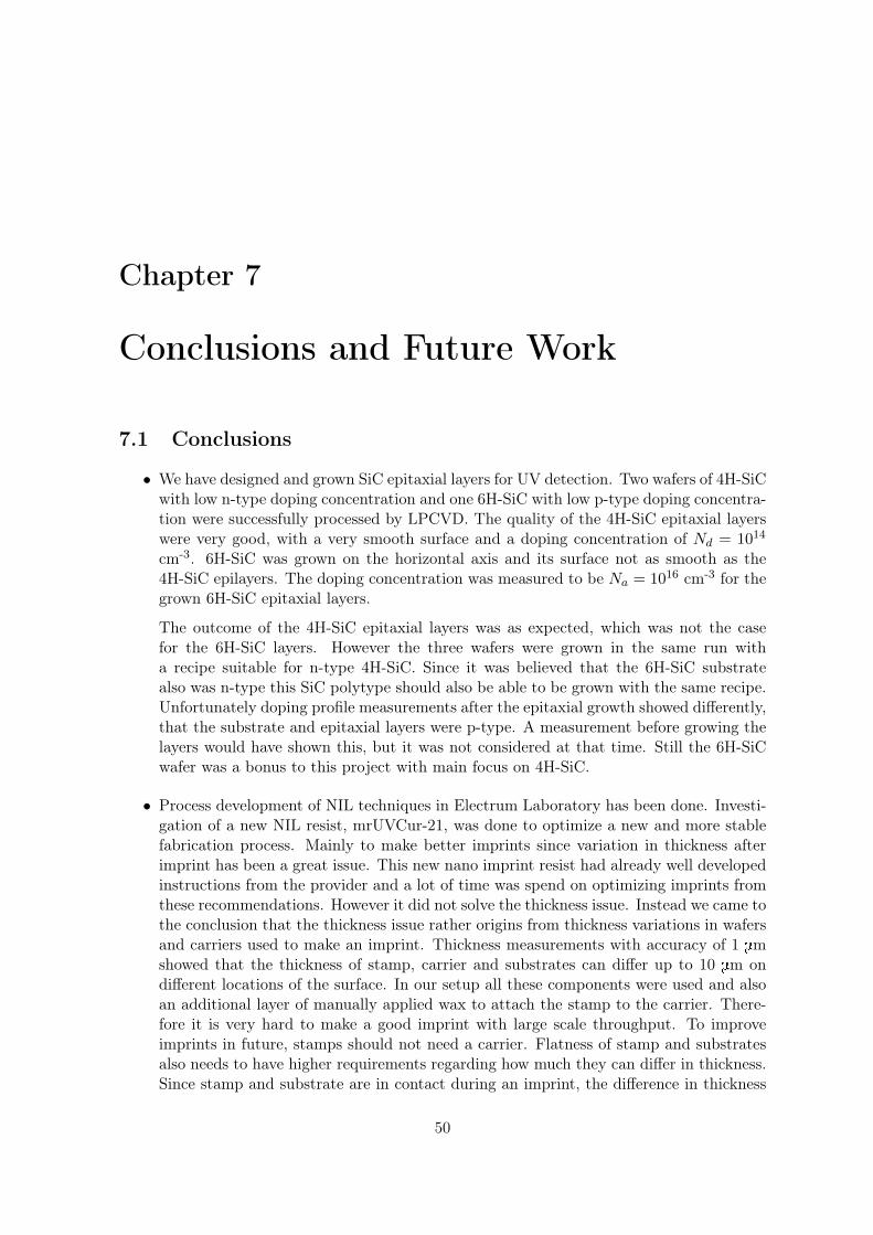
Chapter 7
Conclusions and Future Work
7.1 Conclusions
• We have designed and grown SiC epitaxial layers for UV detection. Two wafers of 4H-SiCwith low n-type doping concentration and one 6H-SiC with low p-type doping concentra-tion were successfully processed by LPCVD. The quality of the 4H-SiC epitaxial layerswere very good, with a very smooth surface and a doping concentration of Nd = 1014
cm-3. 6H-SiC was grown on the horizontal axis and its surface not as smooth as the4H-SiC epilayers. The doping concentration was measured to be Na = 1016 cm-3 for thegrown 6H-SiC epitaxial layers.
The outcome of the 4H-SiC epitaxial layers was as expected, which was not the casefor the 6H-SiC layers. However the three wafers were grown in the same run witha recipe suitable for n-type 4H-SiC. Since it was believed that the 6H-SiC substratealso was n-type this SiC polytype should also be able to be grown with the same recipe.Unfortunately doping profile measurements after the epitaxial growth showed differently,that the substrate and epitaxial layers were p-type. A measurement before growing thelayers would have shown this, but it was not considered at that time. Still the 6H-SiCwafer was a bonus to this project with main focus on 4H-SiC.
• Process development of NIL techniques in Electrum Laboratory has been done. Investi-gation of a new NIL resist, mrUVCur-21, was done to optimize a new and more stablefabrication process. Mainly to make better imprints since variation in thickness afterimprint has been a great issue. This new nano imprint resist had already well developedinstructions from the provider and a lot of time was spend on optimizing imprints fromthese recommendations. However it did not solve the thickness issue. Instead we came tothe conclusion that the thickness issue rather origins from thickness variations in wafersand carriers used to make an imprint. Thickness measurements with accuracy of 1 mmshowed that the thickness of stamp, carrier and substrates can differ up to 10 mm ondifferent locations of the surface. In our setup all these components were used and alsoan additional layer of manually applied wax to attach the stamp to the carrier. There-fore it is very hard to make a good imprint with large scale throughput. To improveimprints in future, stamps should not need a carrier. Flatness of stamp and substratesalso needs to have higher requirements regarding how much they can differ in thickness.Since stamp and substrate are in contact during an imprint, the difference in thickness
50
should not be larger and preferably much smaller than the hight of the structures in thestamp.
Attempts to replicate a test stamp and the master stamp used in this project wereperformed. However this process was never fully developed for full functionality andreliability. We came to the conclusion that another type of anti sticking layer should beused for replicated stamps. An anti sticking agent was found for this purpose, but therewas no time for further investigation here since it required a new more complex processfor deposition of the chemical.
• Micro scale UV detectors in 4H- and 6H-SiC has successfully been fabricated with goodresults and performance. Compared to a previous project where MSM UV photode-tectors here made in GaN the performance was improved regarding the signal to noiseratio, which is the same as photocurrent to dark current ratio in this case. There areseveral reasons for this, but we believe that it mainly has to do with material qualityand the Schottky barrier height of the devices.
• Shrinking of 4H-SiC UV detectors from micro- to nano-scale has successfully beendemonstrated using nano imprint lithography. This has not been done before on SiC,but in the previous project just mentioned it has been done using GaN as substrate.However the throughput in the device fabrication was increased and nano-scale MSM de-vices were also made on InSb and on InAs QDs for future investigation. The nano-scaleMSM devices on 4H-SiC had a better signal to noise ratio compared to nano-scale MSMdevices on GaN. The reason for this is believed to be the same as for the micro-scaledevices just mentioned.
• Measurements that has been performed of fabricated MSM UV photodetectors concernelectrical and optical performance, such as dark current, photocurrent and spectral re-sponse.
7.2 Future Work
• Devices should be optimized by deeper investigation of which combination of devicegeometry that gives highest efficiency by analyzing photocurrents.
• High resolution time response measurements should be performed of fabricated devicessince it is believed that the nano-scale devices have a faster response than in micro-scale.
• 2D array should be fabricated for UV imaging.
• Development of the nano imprint lithography should be done. Especially regardingdevelopment of a fully functional stamp replication process and a lift-off process thatsuits NIL.
51
Bibliography
[1] Andreas Bergström. Fabrication of nano detectors/sensors by nano imprint lithography.Master’s thesis, KTH, 2010.
[2] Sy Chou and My Liu. Nanoscale Tera-Hertz Metal-Semiconductor-Metal Photodetectors.IEEE Journal of Quantum Electronics, 28(10):2358–2368, Oct 1992.
[3] Wikipedia. Silicon Carbide, 2010. http://en.wikipedia.org/wiki/Silicon_carbideAccessed 30 Oct 2010.
[4] NSM Archive. Silicon Carbide, 2009. http://www.ioffe.rssi.ru/SVA/NSM/Semicond/SiC/ Accessed 30 Oct 2010.
[5] Sima Dimitrijev. Principles of semiconductor devices. Oxford University Press, NewYork, 2006.
[6] Jasprit Singh. Semiconductor devices : basic principles. Wiley, New York, 2000.
[7] Carl Nordling. Physics handbook for science and engineering. Studentlitteratur, Lund,2006.
[8] S. Davydov. On the electron affinity of silicon carbide polytypes. Semiconductors, 41:696–698, 2007. 10.1134/S1063782607060152.
[9] Sarah Youngbauer. AMD Fusion APU Era Begins, Jan 2011. http://www.amd.com/us/press-releases/Pages/amd-fusion-apu-era-2011jan04.aspx Accessed 21 May 2011.
[10] Michael D. Austin, Haixiong Ge, Wei Wu, Mingtao Li, Zhaoning Yu, D. Wasserman,S. A. Lyon, and Stephen Y. Chou. Fabrication of 5 nbsp;nm linewidth and 14 nbsp;nmpitch features by nanoimprint lithography. Applied Physics Letters, 84(26):5299 –5301,jun 2004.
[11] E. S. M. Goh, T. P. Chen, C. Q. Sun, L. Ding, and Y. Liu. Design of a near-perfect antireflective layer for si photodetectors based on a sio2 film embedded with si nanocrystals.Japanese Journal of Applied Physics, 48(6), 2009.
[12] Rei Kitamura, Laurent Pilon, and Miroslaw Jonasz. Optical constants of silica glass fromextreme ultraviolet to far infrared at near room temperature. Appl. Opt., 46(33):8118–8133, Nov 2007.
[13] M. Siad, C. Pineda Vargas, M. Nkosi, D. Saidi, N. Souami, N. Daas, and A.C. Chami.Characterisation of ni and ni/ti contact on n-type 4h-sic. Applied Surface Science,256(1):256 – 260, 2009.
52

[14] J. Schrauwen. Polymer wedge for perfectly vertical light coupling to silicon. IntegratedOptics: Devices, materials and technologies XIII, 7218: - 2009, 7218 p72180B (8 pages),2009.
[15] Antonella Sciuto, Fabrizio Roccaforte, Salvatore Di Franco, Vito Raineri, and GiovanniBonanno. High responsivity 4H-SiC Schottky UV photodiodes based on the pinch-offsurface effect. Applied Physics Letters, 89(8), AUG 21 2006.
53

Appendix A
4H- and 6H-SiC UV photodetectors
Presented in The 16th Semiconducting and Insulating Materials Conference (SIMC-XVI 2011)and accepted by Physica Status Solidi.
54
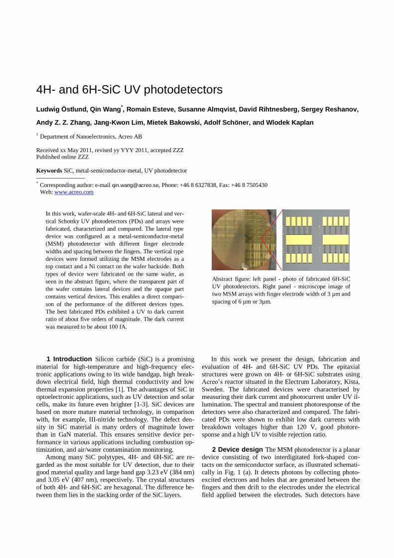
4H- and 6H-SiC UV photodetectors
Ludwig Östlund, Qin Wang*, Romain Esteve, Susanne Almqvist, David Rihtnesberg, Sergey Reshanov,
Andy Z. Z. Zhang, Jang-Kwon Lim, Mietek Bakowski, Adolf Schöner, and Wlodek Kaplan
1 Department of Nanoelectronics, Acreo AB
Received xx May 2011, revised yy YYY 2011, accepted ZZZ Published online ZZZ
Keywords SiC, metal-semiconductor-metal, UV photodetector
* Corresponding author: e-mail [email protected], Phone: +46 8 6327838, Fax: +46 8 7505430 Web: www.acreo.com
In this work, wafer-scale 4H- and 6H-SiC lateral and ver-
tical Schottky UV photodetectors (PDs) and arrays were
fabricated, characterized and compared. The lateral type
device was configured as a metal-semiconductor-metal
(MSM) photodetector with different finger electrode
widths and spacing between the fingers. The vertical type
devices were formed utilizing the MSM electrodes as a
top contact and a Ni contact on the wafer backside. Both
types of device were fabricated on the same wafer, as
seen in the abstract figure, where the transparent part of
the wafer contains lateral devices and the opaque part
contains vertical devices. This enables a direct compari-
son of the performance of the different devices types.
The best fabricated PDs exhibited a UV to dark current
ratio of about five orders of magnitude. The dark current
was measured to be about 100 fA.
Abstract figure: left panel - photo of fabricated 6H-SiC
UV photodetectors. Right panel - microscope image of
two MSM arrays with finger electrode width of 3 µm and
spacing of 6 µm or 3µm.
1 Introduction Silicon carbide (SiC) is a promising
material for high-temperature and high-frequency elec-tronic applications owing to its wide bandgap, high break-down electrical field, high thermal conductivity and low
thermal expansion properties [1]. The advantages of SiC in optoelectronic applications, such as UV detection and solar cells, make its future even brighter [1-3]. SiC devices are based on more mature material technology, in comparison
with, for example, III-nitride technology. The defect den-sity in SiC material is many orders of magnitude lower than in GaN material. This ensures sensitive device per-
formance in various applications including combustion op-timization, and air/water contamination monitoring.
Among many SiC polytypes, 4H- and 6H-SiC are re-
garded as the most suitable for UV detection, due to their good material quality and large band gap 3.23 eV (384 nm) and 3.05 eV (407 nm), respectively. The crystal structures of both 4H- and 6H-SiC are hexagonal. The difference be-
tween them lies in the stacking order of the SiC layers.
In this work we present the design, fabrication and
evaluation of 4H- and 6H-SiC UV PDs. The epitaxial structures were grown on 4H- or 6H-SiC substrates using Acreo’s reactor situated in the Electrum Laboratory, Kista,
Sweden. The fabricated devices were characterised by measuring their dark current and photocurrent under UV il-lumination. The spectral and transient photoresponse of the detectors were also characterized and compared. The fabri-
cated PDs were shown to exhibit low dark currents with breakdown voltages higher than 120 V, good photore-sponse and a high UV to visible rejection ratio.
2 Device design The MSM photodetector is a planar device consisting of two interdigitated fork-shaped con-
tacts on the semiconductor surface, as illustrated schemati-cally in Fig. 1 (a). It detects photons by collecting photo-excited electrons and holes that are generated between the fingers and then drift to the electrodes under the electrical
field applied between the electrodes. Such detectors have
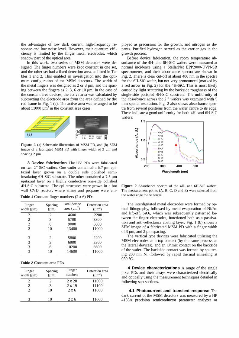
the advantages of low dark current, high-frequency re-sponse and low noise level. However, their quantum effi-ciency is limited by the finger metal electrodes, which
shadow part of the optical area. In this work, two series of MSM detectors were de-
signed. The finger numbers were kept constant in one set, and the other set had a fixed detection area, as listed in Ta-
bles 1 and 2. This enabled an investigation into the opti-mum configuration of the MSM detectors. The width of the metal fingers was designed as 2 or 3 µm, and the spac-
ing between the fingers as 2, 3, 6 or 10 μm. In the case of the constant area devices, the active area was calculated by subtracting the electrode area from the area defined by the red frame in Fig. 1 (a). The active area was arranged to be
about 11000 µm2 in the constant area cases.
Figure 1 (a) Schematic illustration of MSM PD, and (b) SEM
image of a fabricated MSM PD with finger width of 3 µm and
spacing 2 µm.
3 Device fabrication The UV PDs were fabricated
on two 2” SiC wafers. One wafer contained a 6.7 μm epi-taxial layer grown on a double side polished semi-insulating 6H-SiC substrate. The other contained a 7.5 μm epitaxial layer on a highly conductive one-side polished
4H-SiC substrate. The epi structures were grown in a hot wall CVD reactor, where silane and propane were em-
ployed as precursors for the growth, and nitrogen as do-pants. Purified hydrogen served as the carrier gas in the growth process.
Before device fabrication, the room temperature ab-sorbance of the 4H- and 6H-SiC wafers were measured at normal incidence using a StellarNet EPP2000-UVN-SR spectrometer, and their absorbance spectra are shown in
Fig. 2. There is clear cut-off at about 400 nm in the spectra for the 6H-SiC wafer, but not very pronounced (marked by a red arrow in Fig. 2) for the 4H-SiC. This is most likely
caused by light scattering by the backside roughness of the single-side polished 4H-SiC substrate. The uniformity of the absorbance across the 2’’ wafers was examined with 5 mm spatial resolution. Fig. 2 also shows absorbance spec-
tra from several positions from the wafer centre to its edge. These indicate a good uniformity for both 4H- and 6H-SiC wafers.
Figure 2 Absorbance spectra of the 4H- and 6H-SiC wafers.
The measurement points (A, B, C, D and E) were selected from
the wafer edge to the centre.
The interdigitated metal electrodes were formed by op-tical lithography, followed by metal evaporation of Ni/Au and lift-off. SiO2, which was subsequently patterned be-
tween the finger electrodes, functioned both as a passiva-tion and anti-reflectance coating layer. Fig. 1 (b) shows a SEM image of a fabricated MSM PD with a finger width
of 3 µm, and 2 µm spacing. The vertical type devices were fabricated utilizing the
MSM electrodes as a top contact (by the same process as the lateral devices), and an Ohmic contact on the backside
of the wafer. The backside contact was formed by sputter-ing 200 nm Ni, followed by rapid thermal annealing at 950 °C.
4 Device characterizations A range of the single pixel PDs and their arrays were characterized electrically
and optically using the measurement techniques detailed in following sub-sections. 4.1 Photocurrent and transient response The
dark current of the MSM detectors was measured by a HP 4156A precision semiconductor parameter analyzer or
200 300 400 500
0,5
1,0
1,5
Ab
so
rba
nc
e (
A.
U.)
Wavelength (nm)
4HA
4HB
4HC
4HD
4HE
6HA
6HB
6HC
6HD
6HE
Table 1 Constant finger numbers (2 x 6) PDs
Finger
width (µm)
Spacing
(µm)
Total device
area (µm2) Detection area
(µm2)
2 2 4600 2200 2
2 2
3
3 3 3
3
6 10
2
3 6 10
5700
9000 13400
5800
6900 10200 14600
3300
6600 11000
2200
3300 6600
11000
Table 2 Constant area PDs
Finger width (µm)
Spacing (µm)
Finger
numbers Detection area
(µm2)
2
2 2
3
2
3 10
10
2 x 28
2 x 19 2 x 6
2 x 6
11000
11100 11000
11000
(a) (b)
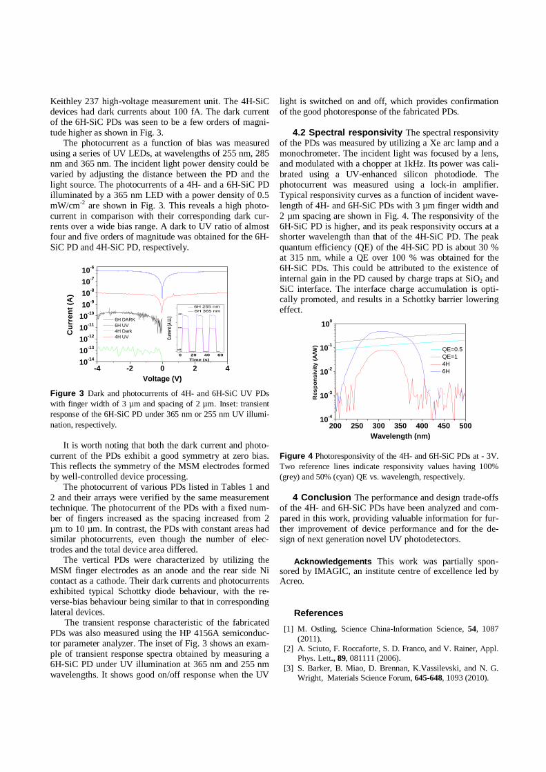
Keithley 237 high-voltage measurement unit. The 4H-SiC devices had dark currents about 100 fA. The dark current of the 6H-SiC PDs was seen to be a few orders of magni-
tude higher as shown in Fig. 3. The photocurrent as a function of bias was measured
using a series of UV LEDs, at wavelengths of 255 nm, 285 nm and 365 nm. The incident light power density could be
varied by adjusting the distance between the PD and the light source. The photocurrents of a 4H- and a 6H-SiC PD illuminated by a 365 nm LED with a power density of 0.5
mW/cm-2 are shown in Fig. 3. This reveals a high photo-current in comparison with their corresponding dark cur-rents over a wide bias range. A dark to UV ratio of almost four and five orders of magnitude was obtained for the 6H-
SiC PD and 4H-SiC PD, respectively.
Figure 3 Dark and photocurrents of 4H- and 6H-SiC UV PDs
with finger width of 3 µm and spacing of 2 µm. Inset: transient
response of the 6H-SiC PD under 365 nm or 255 nm UV illumi-
nation, respectively.
It is worth noting that both the dark current and photo-
current of the PDs exhibit a good symmetry at zero bias. This reflects the symmetry of the MSM electrodes formed by well-controlled device processing.
The photocurrent of various PDs listed in Tables 1 and
2 and their arrays were verified by the same measurement technique. The photocurrent of the PDs with a fixed num-ber of fingers increased as the spacing increased from 2
µm to 10 µm. In contrast, the PDs with constant areas had similar photocurrents, even though the number of elec-trodes and the total device area differed.
The vertical PDs were characterized by utilizing the
MSM finger electrodes as an anode and the rear side Ni contact as a cathode. Their dark currents and photocurrents exhibited typical Schottky diode behaviour, with the re-
verse-bias behaviour being similar to that in corresponding lateral devices. The transient response characteristic of the fabricated
PDs was also measured using the HP 4156A semiconduc-tor parameter analyzer. The inset of Fig. 3 shows an exam-ple of transient response spectra obtained by measuring a 6H-SiC PD under UV illumination at 365 nm and 255 nm
wavelengths. It shows good on/off response when the UV
light is switched on and off, which provides confirmation of the good photoresponse of the fabricated PDs.
4.2 Spectral responsivity The spectral responsivity of the PDs was measured by utilizing a Xe arc lamp and a monochrometer. The incident light was focused by a lens, and modulated with a chopper at 1kHz. Its power was cali-
brated using a UV-enhanced silicon photodiode. The photocurrent was measured using a lock-in amplifier. Typical responsivity curves as a function of incident wave-
length of 4H- and 6H-SiC PDs with 3 µm finger width and 2 µm spacing are shown in Fig. 4. The responsivity of the 6H-SiC PD is higher, and its peak responsivity occurs at a shorter wavelength than that of the 4H-SiC PD. The peak
quantum efficiency (QE) of the 4H-SiC PD is about 30 % at 315 nm, while a QE over 100 % was obtained for the 6H-SiC PDs. This could be attributed to the existence of
internal gain in the PD caused by charge traps at SiO2 and SiC interface. The interface charge accumulation is opti-cally promoted, and results in a Schottky barrier lowering effect.
Figure 4 Photoresponsivity of the 4H- and 6H-SiC PDs at - 3V. Two reference lines indicate responsivity values having 100%
(grey) and 50% (cyan) QE vs. wavelength, respectively.
4 Conclusion The performance and design trade-offs of the 4H- and 6H-SiC PDs have been analyzed and com-pared in this work, providing valuable information for fur-
ther improvement of device performance and for the de-sign of next generation novel UV photodetectors.
Acknowledgements This work was partially spon-sored by IMAGIC, an institute centre of excellence led by Acreo.
References
[1] M. Ostling, Science China-Information Science, 54, 1087
(2011).
[2] A. Sciuto, F. Roccaforte, S. D. Franco, and V. Rainer, Appl.
Phys. Lett., 89, 081111 (2006).
[3] S. Barker, B. Miao, D. Brennan, K.Vassilevski, and N. G.
Wright, Materials Science Forum, 645-648, 1093 (2010).
-4 -2 0 2 410
-14
10-13
10-12
10-11
10-10
10-9
10-8
10-7
10-6
Cu
rre
nt
(A)
Voltage (V)
6H DARK
6H UV
4H Dark
4H UV
0 20 40 60
on
on
Cur
rent
(A.U
.)
Time (s)
6H 255 nm
6H 365 nm
off
200 250 300 350 400 450 50010
-4
10-3
10-2
10-1
100
R
es
po
ns
ivit
y (
A/W
)
Wavelength (nm)
QE=0.5
QE=1
4H
6H
Appendix B
A theoretical and experimentalcomparison of 4H- and 6H-SiC MSMUV photodetectors
Published in proceedings of The 2011 International Conference on Silicon Carbide and RelatedMaterials (ICSCRM 2011).
58
A theoretical and experimental comparison of 4H- and 6H-SiC MSM UV photodetectors
J.-K. Lim1,2,a, L. Östlund1,b, Q. Wang1,c, W. Kaplan1,d, S.A. Reshanov1,e, A. Schöner1,f, M. Bakowski1,g and H.-P. Nee2,h
1Acreo AB, Electrum 236, SE-164 40 Kista, Stockholm, Sweden 2EES/EME, KTH-Royal Institute of Technology, Stockholm, Sweden
[email protected], [email protected], [email protected], [email protected], [email protected], [email protected],
[email protected], [email protected]
Keywords: UV photodetector SiC, MSM (Metal-Semiconductor-Metal), PDs (Photodetectors)
Abstract. This paper reports on fabrication and modeling of 4H- and 6H-SiC metal-semiconductor-metal (MSM) photodetectors (PDs). MSM PDs have been fabricated on 4H-SiC and 6H-SiC epitaxial layers, and their performance analyzed by MEDICI simulation and measurements. The simulations were also used to optimize the sensitivity by varying the width and spacing of the interdigitated electrodes. The fabricated PDs with 2 µm wide metal electrodes and 3 µm spacing between the electrodes exhibited, under UV illumination, a peak current to dark current ratio of 105 and 104 in 4H-SiC and 6H-SiC, respectively. The measured spectral responsivity of 6H-SiC PDs was higher compared to that of 4H-SiC PDs, with a cutoff at 407 nm compared to 384 nm in 4H-SiC PDs. Also the peak responsivity occurred at a shorter wavelength in 6H material. A high rejection ratio between the photocurrent and dark current was found in both cases. These experimental results were in agreement with simulation.
Introduction Silicon carbide (SiC) is a very attractive material for UV photodetectors (PDs) due to its wide bandgap and high absorption coefficient in the UV region. Owing to its material maturity and stability, detectors utilizing 4H- and 6H-SiC (bandgap of 3.23 eV and 3.05 eV, respectively) have the advantage of a good photoresponse with a very low dark current, and can also operate in harsh environments. In recent years, SiC UV PDs have been the subject of many publications that demonstrate their potential [1, 2]. Different measures to improve the sensitivity of the devices have been investigated, such as the use of semitransparent electrodes [3], structural design [4] and avalanche detectors with novel embedded structures [5]. Also theoretical work which improves the absorption models for 4H-SiC at short wavelengths has been published [6]. In this paper, we compare the performance of 4H- and 6H-SiC MSM UV PDs by simulation and experiment, taking into consideration inherent material properties and optimization of the device performance.
Device design and fabrication
A top view of the fabricated detector is shown in Fig 1. The two terminal device consists of two interdigitated Schottky electrodes in the so-called back-to-back configuration. It detects photons by collecting photo-excited electrons and holes that are generated between the fingers and then drift to the electrodes under the influence of the electric field. The cross-section of the fabricated and simulated structure is shown in Fig 2. The optically exposed layer, in the case of the 4H-SiC PD, is a 7.5 µm thick epitaxial layer, with a doping level of 1014 cm-3 grown on a highly conductive one-side polished 4H-SiC substrate. In the case of the 6H-SiC PD, the epitaxial layer is 6.7 µm thick, with a doping level of 1016 cm-3, grown on a double side polished semi-insulating 6H-SiC substrate.
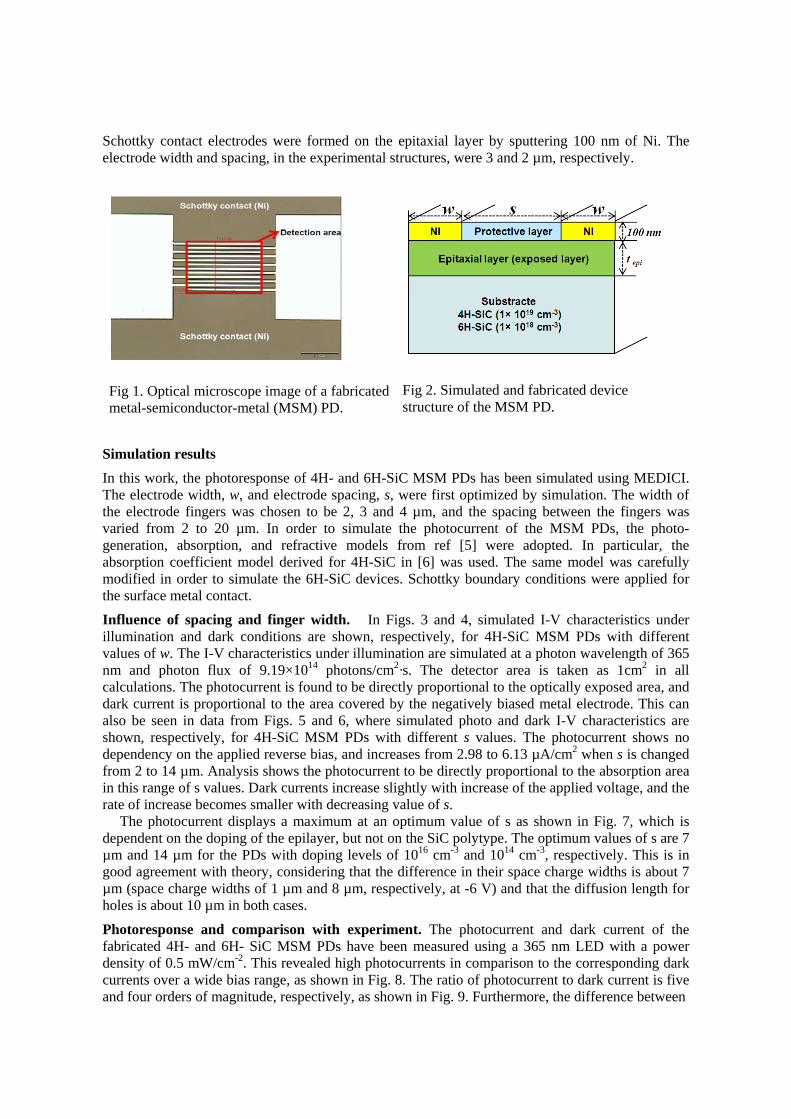
Schottky contact electrodes were formed on the epitaxial layer by sputtering 100 nm of Ni. The electrode width and spacing, in the experimental structures, were 3 and 2 µm, respectively.
Fig 1. Optical microscope image of a fabricated metal-semiconductor-metal (MSM) PD.
Fig 2. Simulated and fabricated device structure of the MSM PD.
Simulation results
In this work, the photoresponse of 4H- and 6H-SiC MSM PDs has been simulated using MEDICI. The electrode width, w, and electrode spacing, s, were first optimized by simulation. The width of the electrode fingers was chosen to be 2, 3 and 4 µm, and the spacing between the fingers was varied from 2 to 20 µm. In order to simulate the photocurrent of the MSM PDs, the photo-generation, absorption, and refractive models from ref [5] were adopted. In particular, the absorption coefficient model derived for 4H-SiC in [6] was used. The same model was carefully modified in order to simulate the 6H-SiC devices. Schottky boundary conditions were applied for the surface metal contact.
Influence of spacing and finger width. In Figs. 3 and 4, simulated I-V characteristics under illumination and dark conditions are shown, respectively, for 4H-SiC MSM PDs with different values of w. The I-V characteristics under illumination are simulated at a photon wavelength of 365 nm and photon flux of 9.19×10¹⁴ photons/cm2·s. The detector area is taken as 1cm2 in all calculations. The photocurrent is found to be directly proportional to the optically exposed area, and dark current is proportional to the area covered by the negatively biased metal electrode. This can also be seen in data from Figs. 5 and 6, where simulated photo and dark I-V characteristics are shown, respectively, for 4H-SiC MSM PDs with different s values. The photocurrent shows no dependency on the applied reverse bias, and increases from 2.98 to 6.13 µA/cm2 when s is changed from 2 to 14 µm. Analysis shows the photocurrent to be directly proportional to the absorption area in this range of s values. Dark currents increase slightly with increase of the applied voltage, and the rate of increase becomes smaller with decreasing value of s.
The photocurrent displays a maximum at an optimum value of s as shown in Fig. 7, which is dependent on the doping of the epilayer, but not on the SiC polytype. The optimum values of s are 7 µm and 14 µm for the PDs with doping levels of 1016 cm-3 and 1014 cm-3, respectively. This is in good agreement with theory, considering that the difference in their space charge widths is about 7 µm (space charge widths of 1 µm and 8 µm, respectively, at -6 V) and that the diffusion length for holes is about 10 µm in both cases.
Photoresponse and comparison with experiment. The photocurrent and dark current of the fabricated 4H- and 6H- SiC MSM PDs have been measured using a 365 nm LED with a power density of 0.5 mW/cm-2. This revealed high photocurrents in comparison to the corresponding dark currents over a wide bias range, as shown in Fig. 8. The ratio of photocurrent to dark current is five and four orders of magnitude, respectively, as shown in Fig. 9. Furthermore, the difference between
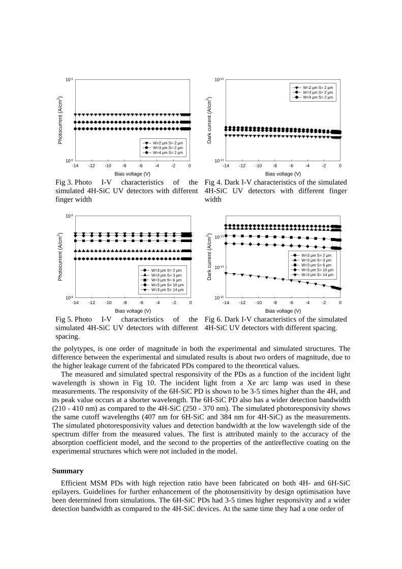
Bias voltage (V)-14 -12 -10 -8 -6 -4 -2 0
Pho
tocu
rren
t (A
/cm
2 )
10-6
10-5
W=2 µm S= 2 µm W=3 µm S= 2 µmW=4 µm S= 2 µm
Bias voltage (V)-14 -12 -10 -8 -6 -4 -2 0
Dar
k cu
rren
t (A
/cm
2 )
10-13
10-12
W=2 µm S= 2 µm W=3 µm S= 2 µmW=4 µm S= 2 µm
Fig 3. Photo I-V characteristics of the simulated 4H-SiC UV detectors with different finger width
Fig 4. Dark I-V characteristics of the simulated 4H-SiC UV detectors with different finger width
Bias voltage (V)-14 -12 -10 -8 -6 -4 -2 0
Pho
tocu
rren
t (A
/cm
2 )
10-6
10-5
W=3 µm S= 2 µm W=3 µm S= 3 µm W=3 µm S= 6 µm W=3 µm S= 10 µm W=3 µm S= 14 µm
Bias voltage (V)-14 -12 -10 -8 -6 -4 -2 0
Dar
k cu
rren
t (A/
cm2 )
10-15
10-14
10-13
W=3 µm S= 2 µm W=3 µm S= 3 µm W=3 µm S= 6 µm W=3 µm S= 10 µm W=3 µm S= 14 µm
Fig 5. Photo I-V characteristics of the simulated 4H-SiC UV detectors with different spacing.
Fig 6. Dark I-V characteristics of the simulated 4H-SiC UV detectors with different spacing.
the polytypes, is one order of magnitude in both the experimental and simulated structures. The difference between the experimental and simulated results is about two orders of magnitude, due to the higher leakage current of the fabricated PDs compared to the theoretical values.
The measured and simulated spectral responsivity of the PDs as a function of the incident light wavelength is shown in Fig 10. The incident light from a Xe arc lamp was used in these measurements. The responsivity of the 6H-SiC PD is shown to be 3-5 times higher than the 4H, and its peak value occurs at a shorter wavelength. The 6H-SiC PD also has a wider detection bandwidth (210 - 410 nm) as compared to the 4H-SiC (250 - 370 nm). The simulated photoresponsivity shows the same cutoff wavelengths (407 nm for 6H-SiC and 384 nm for 4H-SiC) as the measurements. The simulated photoresponsivity values and detection bandwidth at the low wavelength side of the spectrum differ from the measured values. The first is attributed mainly to the accuracy of the absorption coefficient model, and the second to the properties of the antireflective coating on the experimental structures which were not included in the model.
Summary
Efficient MSM PDs with high rejection ratio have been fabricated on both 4H- and 6H-SiC epilayers. Guidelines for further enhancement of the photosensitivity by design optimisation have been determined from simulations. The 6H-SiC PDs had 3-5 times higher responsivity and a wider detection bandwidth as compared to the 4H-SiC devices. At the same time they had a one order of
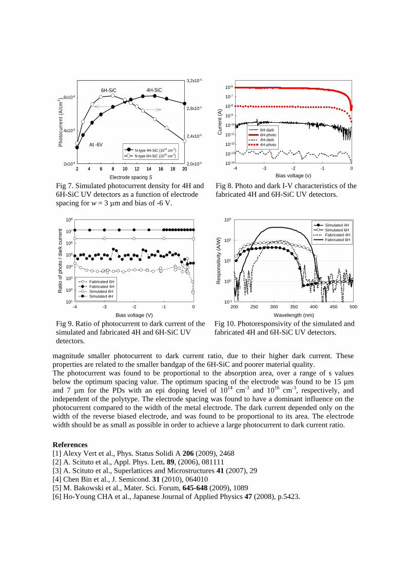
Electrode spacing S2 4 6 8 10 12 14 16 18 20
Phot
ocur
rent
(A/c
m2 )
2x10⁻⁶
4x10⁻⁶
6x10⁻⁶
N-type 4H-SiC (1014 cm-3)
2 4 6 8 10 12 14 16 18 202,0x10⁻⁵
2,4x10⁻⁵
2,8x10⁻⁵
3,2x10⁻⁵
N-type 6H-SiC (1016 cm-3)
At -6V
6H-SiC 4H-SiC
Bias voltage (v)-4 -3 -2 -1 0
Cur
rent
(A)
10-14
10-13
10-12
10-11
10-10
10-9
10-8
10-7
10-6
6H-dark 6H-photo4H-dark 4H-photo
Fig 7. Simulated photocurrent density for 4H and 6H-SiC UV detectors as a function of electrode spacing for w = 3 µm and bias of -6 V.
Fig 8. Photo and dark I-V characteristics of the fabricated 4H and 6H-SiC UV detectors.
Bias voltage (V)-4 -3 -2 -1 0
Rat
io o
f pho
to /
dark
cur
rent
101
102
103
104
105
106
107
108
Fabricated 6HFabricated 4HSimulated 6HSimulated 4H
Fig 9. Ratio of photocurrent to dark current of the simulated and fabricated 4H and 6H-SiC UV detectors.
Wavelength (nm)200 250 300 350 400 450 500
Res
pons
itivi
ty (A
/W)
10-1
100
101
102
103
Simulated 4HSimulated 6HFabricated 4HFabricated 6H
Fig 10. Photoresponsivity of the simulated and fabricated 4H and 6H-SiC UV detectors.
magnitude smaller photocurrent to dark current ratio, due to their higher dark current. These properties are related to the smaller bandgap of the 6H-SiC and poorer material quality. The photocurrent was found to be proportional to the absorption area, over a range of s values below the optimum spacing value. The optimum spacing of the electrode was found to be 15 µm and 7 µm for the PDs with an epi doping level of 1014 cm-3 and 1016 cm-3, respectively, and independent of the polytype. The electrode spacing was found to have a dominant influence on the photocurrent compared to the width of the metal electrode. The dark current depended only on the width of the reverse biased electrode, and was found to be proportional to its area. The electrode width should be as small as possible in order to achieve a large photocurrent to dark current ratio.
References [1] Alexy Vert et al., Phys. Status Solidi A 206 (2009), 2468 [2] A. Scituto et al., Appl. Phys. Lett. 89, (2006), 081111 [3] A. Scituto et al., Superlattices and Microstructures 41 (2007), 29 [4] Chen Bin et al., J. Semicond. 31 (2010), 064010 [5] M. Bakowski et al., Mater. Sci. Forum, 645-648 (2009), 1089 [6] Ho-Young CHA et al., Japanese Journal of Applied Physics 47 (2008), p.5423.