fabrication and characterization of silicon carbide power - diva
TRANSCRIPT
Fabrication and Characterization of Silicon Carbide Power Bipolar Junction
Transistors
Hyung-Seok Lee
Doctoral Thesis
KTH, Royal Institute of Technology Department of Microelectronics and Applied Physics (MAP),
Device Technology Laboratory Stockholm, Sweden 2008
KTH Information and Communication Technology
Cover illustration: A photo of a fabricated 4H-SiC on 2-inch Silicon Carbide wafer to the left. A 4H-SiC BJT glued with silver epoxy on DCB substrate to the top-right. A DC measurement with a 4H-SiC BJT to the bottom-right.
Fabrication and Characterization of Silicon Carbide Power Bipolar Junction Transistors
A dissertation submitted to Kungliga Tekniska Högskolan (KTH), Stockholm, Sweden, in partial fulfillment of the requirements for the degree of Teknologie Doktor (Ph.D)
© 2008 Hyung-Seok Lee
TRITA-ICT/MAP AVH 2008:01 ISSN 1653-7610 ISRN KTH/ICT-MAP/AVH-2008:01-SE Forskningsrapport 2008:1
This thesis is available in electronic version at: http://media.lib.kth.se
Printed by Universitetsservice US-AB, Stockholm, 2008

i
To MY PARENTS AND FAMILY

ii

iii
Abstract
Silicon carbide bipolar junction transistors (BJTs) are attractive power switching devices because of the unique material properties of SiC with high breakdown electric field, high thermal conductivity and high saturated drift velocity of electrons. The SiC BJT has potential for very low specific on-resistances and this together with high temperature operation makes it very suitable for applications with high power densities. For SiC BJTs the common emitter current gain (β), the specific on-resistance (RSP_ON), and the breakdown voltage are important to optimize for competition with silicon based power devices. In this thesis, power SiC BJTs with high current gain β ≈ 60 , low on-resistance RSP_ON ≈ 5 mΩcm2, and high breakdown voltage BVCEO ≈ 1200 V have been demonstrated. The 1200 V SiC BJT that has been demonstrated has about 80 % lower on-state power losses compared to a typical 1200 V Si IGBT chip.
A continuous epitaxial growth of the base-emitter layers has been used to reduce interface defects and thus improve the current gain. A significant influence of surface recombination on the current gain was identified by comparing the experiments with device simulations. In order to reduce the surface recombination, different passivation layers were investigated in SiC BJTs, and thermal oxidation in N2O ambient was identified as an efficient passivation method to increase the current gain.
To obtain a low contact resistance, especially to the p-type base contact, is one critical issue to fabricate SiC power BJTs with low on-resistance. Low temperature anneal (~ 800 oC) of a p-type Ni/Ti/Al contact on 4H-SiC has been demonstrated. The contact resistivity on the ion implanted base region of the BJT was 1.3 × 10⁻⁴ Ωcm2 after annealing. The Ni/Ti/Al p-type ohmic contact was adapted to 4H-SiC BJTs fabrication indicating that the base contact plays a role for achieving a low on-resistance of SiC BJTs.
To achieve a high breakdown voltage, optimized junction termination is important in a power device. A guard ring assisted Junction Termination Extension (JTE) structure was used to improve the breakdown voltage of the SiC BJTs. The highest breakdown voltage of the fabricated SiC BJTs was obtained for devices with guard ring assisted JTE using the base contact implant step for a simultaneous formation of guard rings.
As a new approach to fabricate SiC BJTs, epitaxial regrowth of an extrinsic base layer was demonstrated. SiC BJTs without any ion implantation were successfully demonstrated using epitaxial regrowth of a highly doped p-type region and an etched JTE using the epitaxial base. A maximum current gain of 42 was measured for a 1.8 mm × 1.8 mm BJT with a stable and reproducible open base breakdown voltage of 1800 V.
Keywords: silicon carbide, power device, BJT, current gain β, specific on resistance (RSP_ON), breakdown voltage, forward voltage drop, surface recombination, ohmic contact.
Hyung-Seok Lee : Fabrication and Characterization of Silicon Carbide Power Bipolar Junction Transistors, ISRN KTH/ICT-MAP/AVH-2008:01-SE, KTH, Royal Institute of Technology, School of Information and Communication Technology, Stockholm 2008.

iv
Table of Contents
Abstract ...............................................................................................................iii Table of Contents ...................................................................................................................... iv
List of Appended Papers ........................................................................................................... vi
Summary of Appended Papers................................................................................................... x
Acknowledgements ..................................................................................................................xii
List of Symbols & Acronyms.................................................................................................. xiv
1. Introduction ..................................................................................................... 1
2. Material Properties ......................................................................................... 3
2.1 Crystal Structures and Polytypes............................................................................................... 3
2.2 Electrical Properties .................................................................................................................... 4 2.2.1 Wide Bandgap........................................................................................................................................ 4 2.2.2 High Breakdown Electric Field.............................................................................................................. 5 2.2.3 High Thermal Conductivity ................................................................................................................... 7
2.3 Electrical Models of SiC.............................................................................................................. 7 2.3.1 Mobility Model ...................................................................................................................................... 7 2.3.2 Intrinsic Carrier Concentration and Energy Bandgap ............................................................................ 8 2.3.3 Incomplete Ionization............................................................................................................................. 9 2.3.4 Recombination ....................................................................................................................................... 9 2.3.5 Bandgap Narrowing ............................................................................................................................. 10
3. Fabrication Technology for SiC BJTs......................................................... 11
3.1 Crystal and Epitaxial Growth .................................................................................................. 11
3.2 Wafer Cleaning .......................................................................................................................... 15
3.3 Etching........................................................................................................................................ 15
3.4 Lithography................................................................................................................................ 18
3.5 Ion Implantation ........................................................................................................................ 18
3.6 Oxidation and Oxide Deposition .............................................................................................. 20
3.7 Metallization............................................................................................................................... 22
4. Power Bipolar Junction Transistors in SiC................................................ 27
4.1 SiC Power Devices ..................................................................................................................... 27
4.2 Bipolar Junction Transistors .................................................................................................... 31 4.2.1 Background of BJTs............................................................................................................................. 31 4.2.2 Design of SiC BJTs.............................................................................................................................. 32 4.2.3 Common Emitter Current Gain ............................................................................................................ 33 4.2.4 Breakdown Voltage.............................................................................................................................. 36 4.2.5 Specific On-Resistance ........................................................................................................................ 37 4.2.6 Mask Layout and Fabrication Process for SiC BJTs............................................................................ 38
5. SiC Power BJTs Results ............................................................................... 45
5.1 Current Gain SiC BJTs............................................................................................................. 45
5.2 Forward Voltage Drop .............................................................................................................. 50

v
5.3 Breakdown Voltage ................................................................................................................... 53
5.4 SiC BJT without Ion-Implantation .......................................................................................... 54
5.5 Comparison of Si IGBT and SiC BJT...................................................................................... 57
5.6 Switching Measurements .......................................................................................................... 57
5.7 Transmission Electron Microscope (TEM) Analysis.............................................................. 58
5.8 High Temperature and High Current Measurements ........................................................... 59
6. Summary, Conclusions and Future Outlook.............................................. 61
Bibliography....................................................................................................... 65
Appended Papers............................................................................................... 75

vi
List of Appended Papers
I. 1200 V, 5.2 mΩcm2 4H-SiC BJTs with a high current gain
H.-S. Lee, M. Domeij, C-M. Zetterling, M. Östling, F. Allerstam and E.Ö. Sveinbjörnsson IEEE Electron Device Letters, vol. 28, no 11, pp. 1007-1009, 2007
II. A comparative study of surface passivation on SiC BJTs with high current gain H.-S. Lee, M. Domeij, C-M. Zetterling, M. Östling, and E.Ö. Sveinbjörnsson Materials Science Forum vol. 556-557, pp. 631-634, 2007 III. 4H-SiC power BJTs with high current gain and low on-resistance H.-S. Lee, M. Domeij, C-M. Zetterling, and M. Östling Materials Science Forum vol. 556-557, pp. 767-770, 2007 IV. Geometrical effects in high current gain 1100 V 4H-SiC BJTs M. Domeij, H.-S. Lee, C-M. Zetterling, M. Östling, and A. Schöner IEEE Electron Device Letters, vol. 26, no 10, pp. 743-745, 2005 V. Influence of the base contact on the electrical characteristics of SiC BJTs H.-S. Lee, M. Domeij, C-M. Zetterling, and M. Östling in Proc. IEEE International Symposium on Power Semiconductor Devices and ICs
(ISPSD) 2007, pp. 153-156, 2007 VI. A 4H-SiC BJT with an Epitaxially Regrown Extrinsic Base Layer E. Danielsson, M. Domeij, H.-S. Lee, C-M. Zetterling, M. Östling, A. Schöner and C.
Hallin Materials Science Forum vol. 483-485, pp. 905-908, 2005 VII. Surface passivation oxide effects on the current gain of 4H-SiC Bipolar Junction
Transistors H.-S. Lee, M. Domeij, C-M. Zetterling, M. Östling, F. Allerstam and E.Ö. Sveinbjörnsson Submitted to Appl. Phys. Lett.
VIII. Low forward voltage drop 4H-SiC BJTs without base contact implantation H.-S. Lee, M. Domeij, C-M. Zetterling, and M. Östling,
Submitted to IEEE Trans. Electron Devices IX. High current gain SiC BJTs with regrown extrinsic base and etched JTE H.-S. Lee, M. Domeij, R. Ghandi, C-M. Zetterling, and M. Östling
Submitted to IEEE Trans. Electron Devices

vii
Related work and other work not included in the thesis
1. Electrical Characteristics of 4H-SiC BJTs at Elevated Temperatures H.-S. Lee, M. Domeij, E. Danielsson, C-M. Zetterling and M. Östling Materials Science Forum Vol. 483-485, pp. 897-900, 2005 2. Investigation of TiW contacts to 4H-SiC Bipolar Junction Devices H.-S. Lee, M. Domeij, C-M. Zetterling, and M. Östling Materials Science Forum vol. 527-529, pp. 887-890, 2006 3. Simulation study of 4H-SiC Junction-gated MOSFETs from 300 K to 773 K H.-S. Lee, S.-M. Koo, C-M. Zetterling, E. Danielsson, M. Domeij, and M. Östling Materials Science Forum vol. 457-460, pp. 1437-1440, 2004 4. High current gain silicon carbide bipolar transistors M. Domeij, H.-S. Lee, C-M. Zetterling, M. Östling, and A. Schöner in Proc. IEEE International Symposium on Power Semiconductor Devices and ICs
(ISPSD) 2006, pp. 141-144, 2006 5. Silicon carbide devices and processes - present status and future perspective M. Östling, H.-S. Lee, M. Domeij, and C-M. Zetterling
Proceedings of the International Conference on Mixed Design of Integrated Circuits ad Systems (MIXDES), pp. 34-42, 2006
6. 1200 V 4H-SiC BJTs with a common emitter current gain of 60 and low on-
resistance H.-S.Lee, M. Domeij, C-M. Zetterling, M. Östling, F. Allerstam and E.Ö.
Sveinbjörnsson To be published in Materials Science Forum 2007 7. Analysis of the base current and the saturation voltage in 4H-SiC power BJTs M. Domeij, H.-S. Lee, C-M. Zetterling, M. Östling, A. Schöner Proceedings of the 12th European conference on Power electronics and applications
(EPE), Aalborg, Denmark 2nd-5th September 2007 8. Backside Nickel Based Ohmic Contacts to N-type Silicon Carbide R.Ghandi, H.-S. Lee, M. Domeij, C-M. Zetterling, and M. Östling To be published in Materials Science Forum 2007 9. Current gain dependence on emitter width in 4H-SiC BJTs M. Domeij, H.-S. Lee, C-M. Zetterling, M. Östling, A. Schöner Materials Science Forum vol. 527-529, pp. 1425-1428, 2006

viii
10. SiC power bipolar junction transistors-Modeling and improvement of the current gain M. Domeij, H.-S. Lee, C-M. Zetterling, M. Östling, and A. Schöner Proceedings of the 11th European conference on Power electronics and applications
(EPE), Dresden, Germany 11th-14th September 2005 11. Current Gain of 4H-SiC Bipolar Transistors Including the Effect of Interface
States M. Domeij, E. Danielsson, H.-S. Lee, C-M. Zetterling and M. Östling Materials Science Forum vol. 483-485, pp. 889-892, 2005 12. SiC JMOSFETs for High-Temperature Stable Circuit Operation S.-M. Koo, C.-M. Zetterling, H.-S. Lee, and M. Östling
Materials Science Forum vol. 457-460, pp. 1445-1450, 2004 13. Combination of JFET and MOSFET devices in 4H-SiC for high-temperature
stable circuit operation S-M. Koo, C-M. Zetterling. H.-S. Lee and M. Östling
Electronics Letters, vol. 39, n 12, pp. 933-935, 2003 14. Challenges for high temperature silicon carbide electronics C.-M. Zetterling, S.-M. Koo, E. Danielsson, .W. Liu, S-K. Lee. M. Domeij, H.-S. Lee,
and M. Östling, Mater. Res. Soc. Symposium Proceedings vol. 764, pp. 15-25, 2003 15. Growth of boron nano-junctions Yun, S.H., Dibos, A., Lee, H.-S., Wu, J.Z., and Karlsson, U.O. Applied Surface Science, v 252, n 15, p 5587-5589, 2007 16. A Simple and reliable electrical method for measuring the junction temperature
and thermal resistance of 4H-SiC power bipolar junction transistors P.Eriksson, M. Domeij, H.-S. Lee, C-M. Zetterling, and M. Östling To be published in Materials Science Forum 2007

ix
Selected Conference Presentations 1. 1200 V 4H-SiC BJTs with a common emitter current gain of 60 and low on-
resistance (Oral) H.-S. Lee, M. Domeij, C-M. Zetterling, M. Östling, F. Allerstam and E.Ö.
Sveinbjörnsson International Conference on Silicon Carbide and Related Materials (ICSCRM), 14th-19th
Oct. Otsu, Japan, 2007 2. Silicon carbide devices and processes - present status and future perspective
(Oral, Invited) M. Östling, H.-S. Lee, M. Domeij, and C-M. Zetterling
Mixed Design of Integrated Circuits ad Systems (MIXDES), Gdynia, Poland, 22nd -24th June, 2006
3. Current gain dependence on emitter width in 4H-SiC BJTs (Oral) M. Domeij, H.-S. Lee, C-M. Zetterling, M. Östling, and A. Schöner International Conference on Silicon Carbide and Related Materials (ICSCRM), 18th-23rd
Sep. Pittsburgh, U.S.A., 2005 4. 4H-SiC power BJTs with high current gain and low on-resistance (Oral) H.-S. Lee, M. Domeij, C-M. Zetterling, and M. Östling European conference on Silicon Carbide and Related Materials (ECSCRM), Sep.
Newcastle, UK, 2006 5. Influence of the base contact on the electrical characteristics of SiC BJTs (Poster) H.-S. Lee, M. Domeij, C-M. Zetterling, and M. Östling
International Symposium on Power Semiconductor Devices and ICs (ISPSD), 27th-30th May, Jeju, Korea, 2007
6. Challenges for high temperature silicon carbide electronics (Oral, Invited) C.-M. Zetterling, S.-M. Koo, E. Danielsson, .W. Liu, S-K. Lee. M. Domeij, H.-S. Lee,
and M. Östling, Mater. Res. Soc. Symposium Spring Meeting, 2003 7. Analysis of the base current and the saturation voltage in 4H-SiC power BJTs
(Poster) M. Domeij, H.-S. Lee, C-M. Zetterling, M. Östling, and A. Schöner the 12th European conference on Power electronics and applications (EPE), Aalborg,
Denmark 2nd-5th September 2007 8. A comparative study of surface passivation on SiC BJTs with high current gain
(Poster) H.-S. Lee, M. Domeij, C-M. Zetterling, M. Östling, and E.Ö. Sveinbjörnsson
European conference on Silicon Carbide and Related Materials (ECSCRM), Sep. Newcastle, UK, 2006

x
Summary of Appended Papers
Paper I. This paper shows a power 4H-SiC bipolar junction transistor (BJT) with high performance (high breakdown, high gain, and low on-resistance). The high gain of the BJT is attributed to a reduction of surface defects leading to reduced surface recombination, obtained when using a passivation by thermal oxidation in N2O ambient. The highest breakdown voltage of SiC BJTs was obtained for devices with guard-ring-assisted JTEs. The author performed all the processing and the electrical characterization and wrote the manuscript. Paper II. This paper presents the effect of the different types of passivation layers on the current gain of SiC BJTs. Measurements have been compared for BJTs passivated with thermal SiO2, plasma deposited (PECVD) SiO2 and BJTs without passivation. BJTs passivated by thermally grown oxide show the highest current gain due to less surface recombination on the etched surface. The author performed all the processing, characterization and analysis and wrote the manuscript. Paper III. This paper investigates the 4H-SiC BJTs with varying geometrical designs. Optimum emitter finger widths and base-contact implant distances have been derived from measurement. The temperature dependent DC I-V characteristics of the BJTs have been studied in this work. Forward-bias stress on SiC BJTs has been also investigated with a reduction of the initial current gain. Resistive switching measurements with packaged SiC BJTs are performed. The author performed most of the processing, most of the characterization, and wrote the manuscript. Paper IV. In this paper, the high current gain is attributed to enhanced material quality obtained after a continuous epitaxial growth of the base–emitter layers. BJTs with varying geometry have been fabricated and characterized. A significant influence of surface recombination on the current gain is identified by comparing results for BJTs with different emitter finger widths. The critical distance between implantation and emitter edge has been analyzed by measurements. The author performed all device processing and contributed with electrical measurements and characterization. Paper V. This paper investigates how the specific on-resistance and common emitter current gain of SiC BJTs depend on the base contact resistance. The on-state characteristics of SiC BJTs have been investigated before and after base contact annealing at different temperatures. In this paper, large area BJT has been introduced with low specific on-resistance. The author performed all device processing, characterization, analysis and wrote the manuscript. . Paper VI. This paper presents the SiC BJTs with epitaxial regrowth to form a highly doped extrinsic base layer for a good base ohmic contact. A remaining regrowth spacer at the edge of the

xi
base-emitter junction was proposed to explain a low current gain. Even though the gain was low, this approach shows the possibility to new fabrication method of SiC BJT. The author contributed with device processing and DC measurements.
Paper VII. This paper investigates and compares the effects of the passivation on the 4H-SiC BJTs with two different passivation layers. The lower current gain of BJTs with thermally grown SiO2 in O2 ambient is attributed to higher interface state density and surface recombination, at the interface between SiC and SiO2, compared to BJTs passivated by thermally SiO2 in N2O ambient. The author performed all processing, characterization and wrote the manuscript. Paper VIII. In this paper, 4H-SiC BJT with lowly doped base region without ion-implantation has been successfully demonstrated using Ni/Ti/Al p-type Ohmic contact. Forward voltage drop between BJTs with and without ion-implantation was compared. The current gain of BJTs without ion-implantation shows less sensitivity of distance between the emitter edge and the base contact implant, while at least 3 μm is required to avoid a current gain reduction in BJTs with ion-implantation. The author performed all the processing and characterizations except for the TEM analysis and wrote the manuscript. Paper IX. This paper presents the SiC BJT fabrication without ion-implantation using epitaxial regrowth of a highly doped p-type region and etched JTE. The devices fabricated exhibit high breakdown voltage (~1.9 kV). Also, the fabricated BJTs show that a distance of 2 μm between the emitter edge and the base contact is sufficient to avoid a current gain reduction due to the implantation free process. The author performed all processing, characterization and wrote the manuscript.

xii
Acknowledgements
The present work was written in Sweden, where I did my Ph. D studies at the Royal Institute of Technology (KTH). During that time many people aided and encouraged me in ways to numerous and varied to mention. First and foremost, I wish especially to express my gratitude to my supervisors, Prof. Carl-Mikael Zetterling, Prof. Mikael Östling, and Dr. Martin Domeij, who from the outset, encouraged me in my work, provided me with many details and suggestions for research and carefully read the manuscripts. My principal supervisor Carl-Mikael has taught me valuable lessons in doing research. His talent, excellent intuition power, and broad interests have encouraged and motivated me. I am deeply grateful to Mikael, head of the department and dean of the school of ICT, for providing invaluable support and continuous guidance with his energetic intellectual energy. Martin has furnished invaluable help during my studies. He also has provided many wonderful discussions and fruitful advice both scientifically and personally. He also has given me several chances to visit conferences and to meet specialists of this research area. Without their help, this Thesis would not have been what it is now.
I am very grateful to Bo Hammarlund, CEO of TranSiC and Dr. Carina Zaring for the excellent support of this research, and for many fruitful discussions. Thanks also to Dr. Muhammad Nawaz, and Jan-Olov Svedberg for kind help. I would also like to thank Dr. Gunnar Malm for kind answers about research as well as social issues in Sweden. Special thanks go also to my senior colleague, Sang-Mo Koo, now a Professor at Kwangwoon University. He helped me to accommodate to the new surroundings in Sweden and also shared his research experience in a kind manner. I wish also to record my appreciation to Dr. Sang-Ho Yun for his great support and advice. His attitude as a scientist always kept me going. I am grateful to Prof. Byung-Moo Moon in Korea University for his great advice and consideration. For supporting my work, I would like to my appreciation to the Swedish Energy Agency (Energimyndigheten).
For offering valuable experiment suggestions, I thank Prof. Josef Lutz of Technische Universität Chemnitz. I am indebted to Birk Heinze and Min Chen for their kindness during studying as an exchange student at Chemnitz. I would like to thank Prof. Einar Sveinbjörnsson at Chalmers University of Technology, Dr. Adolf Schöner at Acreo, for their cooperation with passivation oxide and with epi-growth, respectively.
Thanks are also due to Reza Ghandi for sharing the time in clean room and for fun time in Japan. I would like to give thanks to Gunnar Loeb for the experimental assistance and for kind discussion. I am also grateful to Timo Söderqvist for helping me with clean-room equipment and a Korean greeting whenever he meets me with his smile. I would like to Zandra Lundberg for her warm kindness and for helping out.
I am grateful to Dr. Per-Erik Hellström, Dan Haga, Cecilia Aronsson, and Helena Strömberg for processing advice. Many colleagues have offered useful comments and discussions during the studies, and I would like to give particular thanks to Dr. Erik Danielsson, Dr. Erdal-Suvar, Dr. Uwe Zimmerman, Dr. Johan Seger, Ann-Chatrin Lindgren, Dr. Christian Isheden, Dr. Stefan Persson, Dr. Dongping Wu, Dr. Wei Liu, Dr. Martin von Hartman, Prof. Shili Zhang, Dr. YongBin Wang, Christian Ridder, Dr. Julius Hållstedt, Dr. Zhibin Zhang, Yohannes Assefaw-Redda, Zhen Zhang, Jun Luo, M. Reza Koladouz, Valur Gudmundsson, and Jiantong Li, my room mate.

xiii
I wish also to thank to Dr. Nam-Kyun Kim, Dr. Wook Bang, Dr. Sang-Cheol Kim, and Dr. In-Ho Kang at Korea Electrotechnology Research Institute (KERI) for their warm kindness. I would like to thank all the members of the Korean students and researchers association (KOSAS) in Sweden. I am especially grateful to Prof. Jung-Hyuk Koh at Kwangwoon University. Thanks are given to Dr. Jang-Young Kim, Dr. Joo-Hyung Kim, and Hee-Wook You at KMF. I also acknowledge to Ho-Suk Han and Hye-Young Chung’s family for much help and love.
I sincerely wish to thank all members of my family and loved ones, providing all sorts of tangible and intangible support. Especially, I wish to express my deepest gratitude to my parents. They instilled in me the belief that intellectual pursuit is the highest calling, and that ideas do have the power to change people’s lives. Finally, I want to thank my wife Soo-Youn, who remained encouraging and full of useful suggestions. I send gratitude separately to my daughter Yoon-Seo.
Stockholm, February 2008
Hyung-Seok Lee

xiv
List of Symbols & Acronyms
Symbol Meaning BVCEO Common emitter breakdown voltage BVCBO Common base breakdown voltage DB Base minority carrier diffusion coefficient DE Emitter minority carrier diffusion coefficient E Electric field EC Critical electric field Eg Energy Bandgap gc Donor level degeneracy factor gv Acceptor level degeneracy factor IB Base current IC Collector current IE Emitter current JBulk Bulk recombination current density JScr Space charge recombination current density JInj Base-emitter back-injected current density KBSurf Surface recombination current divided by emitter periphery LT Transfer length NB
Base doping concentration NC Effective conduction band density of states Nd Donor concentration Nd
+ Ionized donor concentration NE
Emitter doping concentration NV
Effective valence band density of states n Electron concentration ni Intrinsic carrier concentration p Hole concentration Pdiss Dissipated power q Electron charge RSRH Shockley-Read-Hall recombination rate RAuger Auger recombination rate RC Contact resistance RT Total resistance RTh Thermal impedance Tamb Ambient temperature Tj Junction temperature VB Breakdown voltage VCE Collector-emitter voltage WE Emitter region width WB Base region width α Common-base current gain αT Base transport factor β Common-emitter current gain γ Emitter injection efficiency ρ Resistivity ρc Specific contact resistance

xv
ρs Sheet resistance τ Lifetime τn Electron lifetime τp Hole lifetime Al Aluminium AFM Atomic force Microscopy B Boron BJT Bipolar Junction Transistor CVD Chemical Vapor Deposition C Carbon DMOSFET Double-diffused MOSFET DIMOSFET Double-Implanted MOSFET EDS Energy Dispersive X-Ray Spectrometry FET Field Effect Transistor GaAS Gallium arsenide GaN Gallium nitride GTO Gate turn-off thyristor ICP Inductively coupled Plasma IGBT Insulated Gate Bipolar Transistor I-V Current-Voltage measurement JBS Junction Barrier Schottky JFET Junction FET JTE Junction Termination Extension LPE Liquid Phase Epitaxy MBE Molecular Beam Epitaxy MOS Metal Oxide Semiconductor MOSFET Metal Oxide Semiconductor Field Effect Transistor Ni Nickel NO Nitric oxide N2O Nitrous oxide PECVD Plasma Enhanced Chemical Vapor Deposition RF Radio Frequency RIE Reactive Ion Etching RTA Rapid Thermal Annealing SBD Schottky barrier diode Si Silicon SiC Silicon Carbide SiO2 Silicon dioxide SIMS Secondary Ion Mass Spectrometry TEM Transmission Electron Microscopy Ti Titanium TiW Titanium Tungsten TLM Tranfer Length Method UMOSFET U-shaped groove MOSFET

xvi

1
Chapter 1
Introduction The beginning of industrial revolution of 18th century has brought about a remarkable change of modern-day society with high living standard. The high energy consumption has been positioned in the center of this revolution. However, environmental pollution to mankind by increased energy consumption has been becoming one of the big issues [1]. Global warming induced by carbon dioxide (CO2) emission has become a global warning to the human society. We are more recognizing the importance of energy saving and efficiency compared to before. The power electronics with demand of energy efficiency is one of the most rapidly progressing technologies during the last decades. Without doubt, the development of power semiconductor devices has become a major force in power electronics which has led to remarkable change of society. Silicon (Si) has been the dominant material in power semiconductor device technology, due to well controlled and mature process technology. Silicon Insulated Gate Bipolar transistors (IGBTs) and power MOSFETs are widely used and dominate the market for power switches. However, the power switching devices in silicon are approaching their theoretical limits [2]. The power transistors for 600 V and above based on Si have either a relatively high specific on-resistance, as the MOSFET, or significant switching power losses as the IGBT, both resulting in high power dissipation. In addition, the maximum allowed operating temperature of Si power devices is typically 150-175 °C, so the design margins to avoid overheating are relatively small. In recent years, the need for a new material for power devices has been stressed because of the limitation of Si material properties and the increasing power densities of power electronic systems. Silicon carbide (SiC) has gained remarkable attention as the most mature of the wide band gap materials (3.0-3.3 eV) with the potential of replacing Si in power devices due to its electrical and physical properties. SiC has the advantage of high thermal conductivity (3-4 W/cmK), high breakdown electric field (2.2·106 V/cm), and high saturated carrier velocity (2·107 cm/s) compared to other semiconductor materials, which makes it an ideal material for power devices [3]. Up to now the material quality and the diameter of SiC wafers
H.-S. LEE Chapter 1. Introduction
2
have been improved. Presently, 3-inch 4H- and 6H- wafers are mainly used for commercial production while research wafers of 4-inch (100 mm) diameter have been already available since 2005. A high power switching device is one of the main device applications for SiC. SiC Schottky diodes are already in commercial production. Many kinds of SiC devices have been progressed to be positioned in the front of commercialization. One of the attractive candidate devices for high power switches is the SiC bipolar junction transistor (BJT) due to very low specific on-resistances and this, together with high temperature operation. Considerable research has been devoted to improve the device performance of BJTs, and especially the common emitter current gain (β), the specific on-resistance, and the breakdown voltage are important factors. The low current gain β of the SiC BJT is one of the main obstacles. However, improvement of β is a complicated problem since β depends in a complex way on the base and emitter doping levels, the material quality and the surface passivation, and detailed study for improvement of β in SiC BJTs is therefore desired. The primary motivation for the research presented in this thesis was to develop and experimentally demonstrate for high performance SiC BJTs. Devices have been fabricated and electrically characterized through seven different process batches. New process technologies are presented in this thesis, enabling improvement of current gain, a low forward voltage drop, and a high breakdown voltage. From optimization of design and process, a state-of-the-art performance SiC BJTs with a high current gain of 60-64, a low forward voltage drop of 0.44 V at 100 A/cm2, and a high breakdown voltage of 1-1.9 kV has been investigated. The topic of this thesis is the fabrication and characterization of SiC BJTs, designed to be used as power switches. This thesis consists of six chapters including this introduction. Chapter 2 presents the material and electrical properties of SiC and makes a comparison with other materials. Chapter 3 describes process technology development for SiC BJTs. In chapter 4, the fundamental and key points of SiC BJTs are described. Results obtained from different fabricated BJTs are discussed in chapter 5. Finally, summary, conclusions, and future outlook are given in chapter 6.

3
3.08 Å
1.89 Å
C
Si
Chapter 2
Material Properties SiC is a semiconductor material exhibiting some important superior characteristics compared with Si or other semiconductors. The wide band gap, the high critical field, the high thermal conductivity are main advantages, which make it an excellent material for high power, high temperature, and high frequency device applications. In this chapter, the basic material properties and advantages of SiC are described. 2.1 Crystal Structures and Polytypes SiC consists of Si and C atoms, which are both group IV element materials. Each Si atom shares electrons with four C atoms, which means that each atom is bonded covalently to four neighbors, and vice versa. The basic structural unit is shown in Fig. 2.1. The approximate bond length between Si and C atoms is 1.89 Å and the length between Si-Si or C-C atoms is 3.08 Å.
Fig. 2.1 The basic structural unit in SiC [5].

H.-S. LEE Chapter 2. Material Properties
4
C
C
A
A
B
B
A
C
A
B
A
B
C
3C 4H 6H
Fig. 2.2 Some common crystal polytypes, 3C, 4H and 6H polytype stacks [5]. SiC has a characteristic, which is known as a polytypism. It means that the material can possess more than one crystal structure. Each crystal structure is called a polytype. The different polytypes are defined by the stacking sequence and referred to by the Ramsdell notation [4]. For instance, 2H, 4H, and 6H is hexagonal structure and has an AB, ABAC, ABCACB stacking sequence, respectively. Similarly, 3C is cubic with ABC stacking sequence. The different stacking sequences for 3C, 4H, and 6H in SiC are illustrated in Fig. 2.2. 2.2 Electrical Properties SiC has a high critical field of about 2·106 V/cm, a high thermal conductivity of 3-4 W/cmK, and a high saturated carrier velocity of 2·107 cm/s. Thanks to these properties, SiC devices have a large potential for high power, high temperature, and high frequency applications. The physical properties of SiC and other semiconductor materials are compared in Table 2.1 [3], [5]-[7].
2.2.1 Wide Bandgap If the electrons in the valence band are excited with an external energy equal to the bandgap, they can move to the conduction band. At a given temperature, the thermal energy creates an intrinsic equilibrium electron-hole pair (EHP) concentration that depends exponentially on the bandgap. At the intrinsic temperature, the EHP concentration becomes equal to the doping

Fabrication and Characterization of SiC Power Bipolar Junction Transistors
5
Table 2.1 Electrical properties of SiC and other semiconductors
Property Si GaAs GaN 3C-SiC 6H-SiC 4H-SiC
Bandgap, Eg (eV at 300K) 1.12 1.43 3.4 2.4 3.0 3.2
Critical field, Ec
(V/cm) 2.5·105 3·105 3·106 2·106 2.5·106 2.2·106
Thermal Conductivity, λ
(W/cmK at 300K) 1.5 0.5 1.3 3-4 3-4 3-4
Saturated electron drift
velocity, vsat (cm/s) 1·107 1·107 2.5·107 2.5·107 2·107 2·107
Electron mobility, μn (cm2/V⋅s) 1350 8500 1000 1000 500 950
Hole mobility, μp (cm2/V⋅s) 480 400 30 40 80 120
Dielectric constant, εr
11.9 13.0 9.5 9.7 10 10
concentration and this normally prevents adequate device operation. The intrinsic temperature depends on doping concentration and for Si a common temperature is around 150 oC. As a wide bandgap material, SiC has three times higher bandgap energy than that of Si. Due to the wide bandgap, the intrinsic temperature of SiC can reach 1000 oC thus making SiC very suitable for high temperature applications. To benefit from the high temperature capability of SiC, developments in package technology are, however, needed.
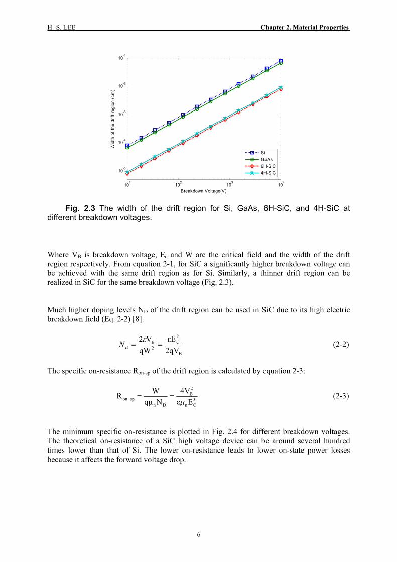
2.2.2 High Breakdown Electric Field Normally, wide bandgap materials have a high breakdown electric field because the wide bandgap leads to a high impact ionization energy. SiC has a high critical field of about 2 MV/cm in a high voltage device. This value is about 10 times higher than that of Si. The breakdown voltage of a p-n diode is given by the following relationship:
2WEV C
B = (2-1)
H.-S. LEE Chapter 2. Material Properties
6
Fig. 2.3 The width of the drift region for Si, GaAs, 6H-SiC, and 4H-SiC at different breakdown voltages.
Where VB is breakdown voltage, Ec and W are the critical field and the width of the drift region respectively. From equation 2-1, for SiC a significantly higher breakdown voltage can be achieved with the same drift region as for Si. Similarly, a thinner drift region can be realized in SiC for the same breakdown voltage (Fig. 2.3).
Much higher doping levels ND of the drift region can be used in SiC due to its high electric breakdown field (Eq. 2-2) [8].
B
2C
2B
2qVεE
qWV2
==ε
DN (2-2)
The specific on-resistance Ron-sp of the drift region is calculated by equation 2-3:
3Cn
2B
Dnspon Eε
4VNqμ
WRμ
==− (2-3)
The minimum specific on-resistance is plotted in Fig. 2.4 for different breakdown voltages. The theoretical on-resistance of a SiC high voltage device can be around several hundred times lower than that of Si. The lower on-resistance leads to lower on-state power losses because it affects the forward voltage drop.
101 102 103 104
10-5
10-4
10-3
10-2
10-1
Breakdown Voltage(V)
Wid
th o
f the
drif
t reg
ion
(cm
)
SiGaAs6H-SiC4H-SiC

Fabrication and Characterization of SiC Power Bipolar Junction Transistors
7
pn,pn,
3001
300
refp,n,
AD
maxp,n,minp,n,pn,
αα μμμ ⎟
⎠⎞
⎜⎝⎛
⎟⎟⎠
⎞⎜⎜⎝
⎛ ++
+⎟⎠⎞
⎜⎝⎛=
T
NNN
T
Fig. 2.4 The minimum specific on resistance of the drift region for Si, GaAs, 6H-SiC, and 4H-SiC as function of breakdown voltage.
2.2.3 High Thermal Conductivity The 2-3 times higher thermal conductivity of SiC compared to Si is an important Figure of merit for high power applications. The generated heat gives a rise in temperature that degrades the device performance and the heating must be limited to avoid device failure. The high thermal conductivity increases the heat transport out from the device. This, together with the low power losses and the high temperature capability, means that a smaller and less expensive thermal cooling system is needed. The thermal cooling system is an important part that affects the cost, size, and weight in power electronic systems. 2.3 Electrical Models of SiC
2.3.1 Mobility Model
The Arora model [9] is commonly used for describing the carrier mobility of SiC.
The low electric field mobility is dependent on the doping level and temperature (see Fig.2.5) and is given by
(2-4)
102 103 10410-3
10-2
10-1
100
101
Breakdown Voltage(V)
Spe
cific
On-
Res
ista
nce(
ohm
cm2 )
Si
GaAS
6H-SiC
4H-SiC

H.-S. LEE Chapter 2. Material Properties
8
ββμ
μμ 1
sat
0pn,
0pn,
pn,
1
)(
⎥⎥
⎦
⎤
⎢⎢
⎣
⎡
⎟⎟⎠
⎞⎜⎜⎝
⎛+
=
vE
E
(a) (b) Fig. 2.5 The low field mobility model of 4H-SiC as a function of doping concentration (a) electron mobility (b) hole mobility.
The high-field velocity is given by the Caughey-Thomas model [10]. At high electric fields, the carrier drift velocity (vD) saturates due to an increase of the optical phonon scattering and reaches the saturation velocity (vsat). The high-field mobility can be expressed as
(2-5)
2.3.2 Intrinsic Carrier Concentration and Energy Bandgap
In an intrinsic semiconductor, the electron density is exactly equal to the hole density. From the mass-action law, we can write this intrinsic-carrier density as
]exp[])(exp[2
kTE
NNkT
EENNn gvc
vcvci
−=
−−= (2-6)
where Eg is the bandgap energy and Nc and Nv are the effective density of states in the conduction and valence bands, respectively. For a given semiconductor material at a constant temperature, the value of ni is constant, and independent of the Fermi energy.
1015
1016
1017
1018
1019
1020
0
100
200
300
400
500
600
700
800
900
1000
Doping concentration(cm-3)
Ele
ctro
n M
obili
ty (c
m2 /V
s)
300 K400 K500 K600 K700 K800 K
1015
1016
1017
1018
1019
1020
0
50
100
150
Doping concentration(cm-3)
Hol
e M
obili
ty (c
m2 /V
s)
300 K400 K500 K600 K700 K800 K

Fabrication and Characterization of SiC Power Bipolar Junction Transistors
9
2.3.3 Incomplete Ionization The donor and acceptor energy levels in SiC are deeper than the thermal energy at room temperature, so the dopants in SiC are not fully ionized even above room temperature [11]-[13].
)exp(1
kTEEg
NNDC
c
DD −
+=+ (2-7)
)exp(1
kTEEg
NNVA
v
AA −
+=+ (2-8)
where EFn and EFp are the quasi-fermi levels, ED and EA is the donor and acceptor energy level, respectively. Due to the lack of specific information for SiC, the donor level degeneracy factor gc and acceptor level degeneracy factor gv are usually assumed to have the same values as in Si. For nitrogen donor levels in 4H-SiC, a dopant ionization energy EC-ED = 42 meV and gc=2 can be used. The p-type doping can be achieved with Al acceptors with ionization energy EA-EV = 191 meV and gv =4 [8].
2.3.4 Recombination Carrier recombination is modeled using the well known Shockley-Read-Hall (SRH) equation. The Shockley-Read-Hall (SRH) recombination rate RSRH can be defined [14]-[15] as
)()(
2
kTE
inkT
E
ip
SRHtraptrap
i
enpenn
nnpR −
+++
−=
ττ (2-9)
Where τn and τp are the electron and hole lifetimes, respectively. These lifetimes depend on temperature, defect concentrations, dopant type and doping concentration. Common SRH carrier lifetimes are in the range of 0.1 – 2 μs in 4H-SiC epitaxial layers [16] but can be significantly reduced in ion implanted material. Auger recombination is a process in which an electron and a hole recombine in a band-to-band transition, with the resulting energy given off to another electron or hole. The Auger recombination rate is given by ))(( 2
iennppCnCR pn
Auger −+= (2-10) where Cn is 5·10-31 [cm-6s-1] and Cp is 2·10-31 [cm-6s-1] [17]-[18].

H.-S. LEE Chapter 2. Material Properties
10
2.3.5 Bandgap Narrowing High concentrations of dopant atoms and free carriers in a semiconductor can cause a significant reduction of the apparent bandgap, so-called bandgap narrowing. At high doping levels, carrier-carrier interaction, carrier-impurity interaction and overlap of the electron wave functions are not negligible. These band gap narrowing effects are taken into account by band edge displacements that can be described [19] as
21
1831
18 )10
()10
(++
+=Δ Dnc
Dncc
NBNAE (2-11)
21
1841
18 )10
()10
(++
+=Δ Dnc
Dnvv
NBNAE (2-12)
Table 2.2 The parameter for bandedge displacement for different polytypes of SiC [19]
n-type Anc Bnc Anv Bnv 4H-SiC -1.5 ×10⁻² -2.93 ×10⁻³ 1.9 ×10⁻² 8.74 ×10⁻³ 6H-SiC -1.12 ×10⁻² -1.01 ×10⁻³ 2.11 ×10⁻² 1.73 ×10⁻³
Bandgap narrowing has an important effect in bipolar transistors by increasing the minority carrier concentration in the emitter, thus reducing the emitter efficiency.

11
Chapter 3
Fabrication Technology for SiC BJTs
One of the main advantages in SiC device technology is the compatibility with Si processing technology compared with other wide bandgap materials. However, there are some differences from Si process technology because of the chemical inertness and the thermal stability of SiC. First of all, wet chemical etching is almost impossible in SiC at room temperature. Instead, plasma etching is available for definition of mesa-etched structures in SiC. The diffusivities of impurities in SiC are orders of magnitude lower than in Si and diffused doping profiles are therefore normally not considered for SiC devices. Generally, ion implantation and epitaxial growth are needed to get proper doping concentrations. Finally, much higher temperatures are needed for thermal oxidation, for annealing of metal ohmic contacts, and for activation of implanted impurities. This chapter will describe process technology for fabrication of SiC BJTs. Figure 3.1 shows the main typical process steps for SiC BJTs. In this work, all process steps have been performed with the polytype 4H-SiC. However, the process technology described in this chapter is valid also for other polytypes of SiC, such as 3C- and 6H-SiC although the process parameters will differ.
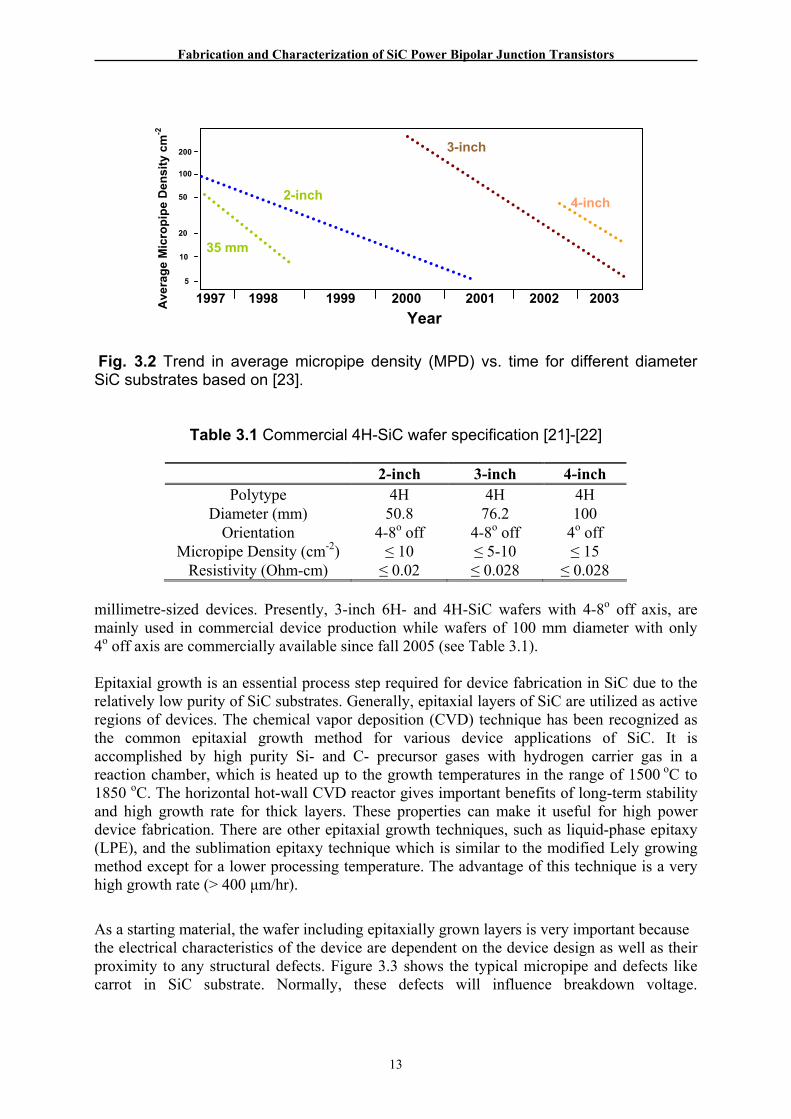
3.1 Crystal and Epitaxial Growth The first SiC material growth was initiated by Acheson. But with the Acheson process the single crystalline material quality was low. Lely later presented a method for single crystal growth in 1955. The Lely method had a limitation in size (< 1 cm2), and could only be used for 6H-SiC, even though high material quality could be obtained. This method was refined by Tairov and Tsvetkov in 1978 [20]. This is now known as the modified Lely method. In earlier days the modified Lely method was used whereas today sublimation growth of SiC is preferred because it can produce large diameter single crystalline SiC boules. The material quality and the diameter of silicon carbide wafers have steadily been improved and the micro-pipe densities have been reduced to ~10 cm-2 for production wafer quality at 4-inch size (see Fig.3.2). For research wafers, as low as ~0.9 cm-2 for a 50 mm 4H-SiC wafer, have been shown [21]-[22]. This is very encouraging for future fabrication of larger than

H.-S. LEE Chapter 3. Fabrication Technology for SiC BJTs
12
Fig. 3.1 The main steps of the SiC BJTs process (a) three epitaxial layers as a starting material (b) oxide deposition with a PECVD process (c) stepper photolithography with a Si 4 inch carrier wafer obtaining high optical resolution (d) oxide dry etching (e) the emitter mesa structure definition by ICP etch with the oxide mask (f) a fabricated transistor after the base mesa etching and metallization steps.
Emitter Base Collector
EmitterBase
Collector
Oxide/Resist
Mask
Emitter
Base
Collector
Oxide/Resist
(a) (b)
Emitter Base Collector
Oxide/Resist
(e) (f)
EmitterBase
Collector
Contact(c) (d)
Fabrication and Characterization of SiC Power Bipolar Junction Transistors
13
Fig. 3.2 Trend in average micropipe density (MPD) vs. time for different diameter SiC substrates based on [23].
Table 3.1 Commercial 4H-SiC wafer specification [21]-[22]
2-inch 3-inch 4-inch Polytype 4H 4H 4H
Diameter (mm) 50.8 76.2 100 Orientation 4-8o off 4-8o off 4o off
Micropipe Density (cm-2) ≤ 10 ≤ 5-10 ≤ 15 Resistivity (Ohm-cm) ≤ 0.02 ≤ 0.028 ≤ 0.028
millimetre-sized devices. Presently, 3-inch 6H- and 4H-SiC wafers with 4-8o off axis, are mainly used in commercial device production while wafers of 100 mm diameter with only 4o off axis are commercially available since fall 2005 (see Table 3.1). Epitaxial growth is an essential process step required for device fabrication in SiC due to the relatively low purity of SiC substrates. Generally, epitaxial layers of SiC are utilized as active regions of devices. The chemical vapor deposition (CVD) technique has been recognized as the common epitaxial growth method for various device applications of SiC. It is accomplished by high purity Si- and C- precursor gases with hydrogen carrier gas in a reaction chamber, which is heated up to the growth temperatures in the range of 1500 oC to 1850 oC. The horizontal hot-wall CVD reactor gives important benefits of long-term stability and high growth rate for thick layers. These properties can make it useful for high power device fabrication. There are other epitaxial growth techniques, such as liquid-phase epitaxy (LPE), and the sublimation epitaxy technique which is similar to the modified Lely growing method except for a lower processing temperature. The advantage of this technique is a very high growth rate (> 400 μm/hr).
As a starting material, the wafer including epitaxially grown layers is very important because the electrical characteristics of the device are dependent on the device design as well as their proximity to any structural defects. Figure 3.3 shows the typical micropipe and defects like carrot in SiC substrate. Normally, these defects will influence breakdown voltage.
1997 1998 1999 2000 2001 2002 2003
5 10
50 100 200
Year
35 mm
2-inch
3-inch
4-inch
20
Ave
rage
Mic
ropi
pe D
ensi
ty c
m-2

H.-S. LEE Chapter 3. Fabrication Technology for SiC BJTs
14
(a) (b)
Fig. 3.3 Surface structure of 4H-Silicon Carbide after device pattering. The optical microscopic in image (a) shows the micro-pipe and defect like carrot (b) shows the defects related with epitaxial growth (4o off axis).
0 10 20 30 40 50 60 70 800.0000
0.0001
0.0002
0.0003
0.0004
0.0005
0.0006
0.0007
Col
lect
or c
urre
nt I c(A
)
Collector Voltage VC (V)
Early Breakdown Voltagedue to the defects
Fig. 3.4 The measured collector current vs. collector voltage. The defects in the SiC surface have a negative influence on the blocking behaviour such as an increased leakage current and in some cases also a reduced breakdown voltage. Carrot defects results in a reduced breakdown voltage compared to the nominal breakdown voltage (see Fig. 3.4) [23]- [24]. Recently, it has been reported that basal plane dislocations (BPDs) in the epilayer is one of the limiting factors for long term stability in SiC bipolar applications. Therefore, the availability of on-axis SiC substrates can impact of reduction of wafer loss as well as reliability. The starting material for the BJT process in this work was 2-inch 4H-SiC substrates. The lowly doped (1015~1017) and highly doped (~1019) epitaxial layers were grown in CVD reactors.
Micropipe
Carrot defects Defects
100 μm
100 μm

Fabrication and Characterization of SiC Power Bipolar Junction Transistors
15
3.2 Wafer Cleaning The surface cleaning of SiC wafer is important to improve the fabrication yield and reduce the uncertainty in process. Normally, RCA clean is widely used as an industry standard to remove the contaminants from wafer. It is useful to remove the organic (SC1) and ionic (SC2) contaminants. The combination of Aceton and propanol can easily remove the photoresist without surface damage. SiC wafer can also be cleaned with the 7-up and IMEC recipes before and during the actual process. The 7-up cleaning is used to remove the most of metal particle. The IMEC cleaning is used to remove the contaminants from the wafer surface and to control the oxide. The summary of cleaning of SiC wafers is shown in Table 3.2.
Table 3.2 Chemicals used for cleaning of SiC wafers
Description Removals Chemicals Temp./Time RCA SC1 Organic H2O:NH4OH:H2O2 (5:1:1) 80-90 oC / 10 minRCA SC2 Ionic, heavy metal H2O:HCl:H2O2 (5:1:1) 80-90 oC / 10 min
7-up Organic/Metal H2SO4:H2O2 (2.5:1) 90-110 oC / 5 min
IMEC Oxide H2O:HF:CH3CH(OH)CH3 (100:1:1) R.T./100 sec
3.3 Etching SiC Etching As mentioned earlier, the strong chemical bond between Si and C makes SiC it difficult to etch. Normally, wet chemical etching of SiC has to be done at high temperature (> 350 oC), but wet chemical etching of SiC has problems because it is relatively isotropic and this prevents etching of steep trenches that are needed in SiC BJTs. Therefore, plasma etching such as RIE and ICP is preferred for etching SiC (see Table 3.3).
Table 3.3 A summary of etching methods for SiC
Technique parameters Polytype of SiC
Etch rate (Å/min) Ref.
Wet chemical Molten KOH 4H 26000 [25] RIE CF4/O2 3C 600-2600 [26]
SF6/O2 6H 3000 [27] CF4/O2 6H 2200 [28] NF3/O2 6H 493 [29] NF3 4H, 6H 1500 [29]
ICP Cl2/Ar 4H 2300 [30] SF6/O2/Ar 4H 5000 [31] SF6 4H 3000 [32]
ECR CF4/O2 4H, 6H 700 [33]
H.-S. LEE Chapter 3. Fabrication Technology for SiC BJTs
16
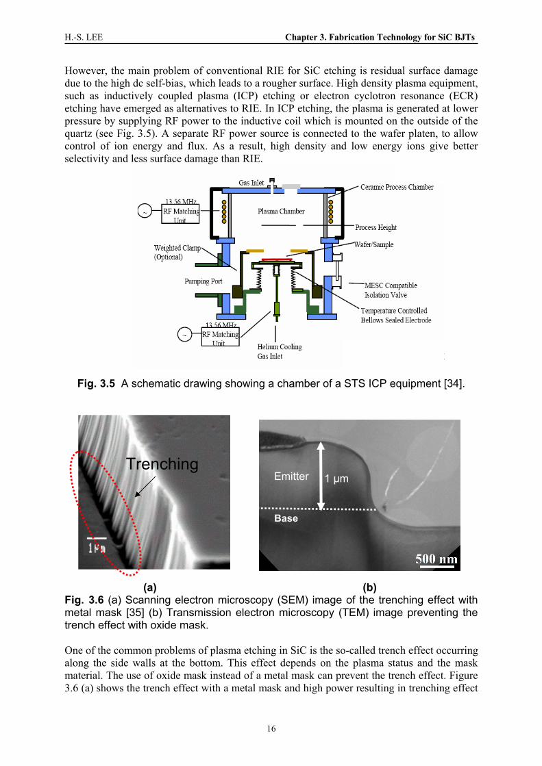
However, the main problem of conventional RIE for SiC etching is residual surface damage due to the high dc self-bias, which leads to a rougher surface. High density plasma equipment, such as inductively coupled plasma (ICP) etching or electron cyclotron resonance (ECR) etching have emerged as alternatives to RIE. In ICP etching, the plasma is generated at lower pressure by supplying RF power to the inductive coil which is mounted on the outside of the quartz (see Fig. 3.5). A separate RF power source is connected to the wafer platen, to allow control of ion energy and flux. As a result, high density and low energy ions give better selectivity and less surface damage than RIE.
Fig. 3.5 A schematic drawing showing a chamber of a STS ICP equipment [34].
(a) (b)
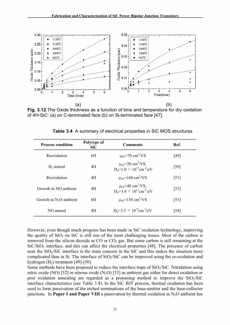
Fig. 3.6 (a) Scanning electron microscopy (SEM) image of the trenching effect with metal mask [35] (b) Transmission electron microscopy (TEM) image preventing the trench effect with oxide mask. One of the common problems of plasma etching in SiC is the so-called trench effect occurring along the side walls at the bottom. This effect depends on the plasma status and the mask material. The use of oxide mask instead of a metal mask can prevent the trench effect. Figure 3.6 (a) shows the trench effect with a metal mask and high power resulting in trenching effect
Trenching 1 μmEmitter
Base

Fabrication and Characterization of SiC Power Bipolar Junction Transistors
17
while showing the smooth edge obtained using an oxide mask and low power during the plasma etching (Fig.3.6 (b)). Using metal etch masks is difficult in some process steps because residual metals can cause contamination in the furnace that is used for thermal oxidation. Therefore, in this work, a fluorine-based (SF6/Ar) ICP reactor was used to etch SiC with an oxide mask. The typical parameters were a SF6 flow rate of 21 sccm, Ar flow rate 9 sccm and 5.0 mTorr base pressure and a plasma deposited silicon dioxide mask was used. The etch rate and the SiC etch selectivity (SiC/SiO2) was around 135 nm/min and 1.47, respectively for 30 W of platen power (see Fig. 3.7 and Fig 3.8).
4 6 8 10 12 14 16 18 20 22 24 26 28 30 3220
30
40
50
60
70
80
90
100
110
120
130
140
150
SiC
Etc
h R
ate
(nm
/min
)
ICP Energy (W) Fig. 3.7 Etch rate as a function of platen power in a STS ICP reactor.
4 6 8 10 12 14 16 18 20 22 24 26 28 30 32
1,15
1,20
1,25
1,30
1,35
1,40
1,45
1,50
Etc
h S
elec
tivity
of S
iC (S
iC/S
iO2)
ICP Energy (W) Fig. 3.8 The SiC/SiO2 etch selectivity as function of platen power.

H.-S. LEE Chapter 3. Fabrication Technology for SiC BJTs
18
Si carrier Wafer
Vaccum Chuck
3.4 Lithography All photolithographic steps were performed using either a Canon 4:1 aligner or a DSW 8500 g-line 5:1 stepper. As positive photoresist, the Shipley 1813 and Shipley 1818 were mainly used, while AZ5214 resist was used for image reversal. The BJTs fabricated in this work were made with 6-9 mask steps depending on the design. The DSW stepper lithography with a Si 4 inch carrier wafer was used to obtain a sufficiently high optical resolution and alignment accuracy (better than 1 μm) in the improved BJT process. Figure 3.9 shows the Si carrier wafer that is used to load the 2 inch SiC wafer and the DSW 8500 g-line 5:1 stepper.
(a)
(b)
Fig. 3.9 The preparation for lithography step (a) 4 inch Si carrier wafer with a center hole to hold SiC wafer (b) the DSW 8500 g-line 5:1 stepper. 3.5 Ion Implantation For SiC processing, ion implantation is the only available technique for selective area doping due to the extremely low diffusion coefficients of dopants in SiC. Ion implantation of SiC bipolar transistors has been used for P-N junction formation [36], highly doped Ohmic contact regions [37]-[39], and device isolation and junction terminations [40]-[43]. For n-type doping, nitrogen (N) and phosphorus (P) are used as typical dopants. Acceptor doping by ion implantation is often used to obtain low contact resistance to p-type regions in pn diodes, BJTs and JFETs. Aluminium (Al) and boron (B) are used for p-type dopants. To minimize lattice damage, ion implantation in SiC is frequently performed at a high temperature in the range of 300 to 800 oC. Acceptor ions are implanted with concentrations between 1017 and 1020 cm-3. Annealing at high temperatures in the range of 1500-1700 °C is essential after ion implantation to activate the implanted dopants and obtain re-crystallisation of the SiC material. There are three important aspects of post-implantation annealing:
(i) To activate implanted dopants (ii) To reduce implantation induced lattice damage
(iii) To preserve the surface morphology and to avoid dopant out diffusion
Si Carrier wafer SiC

Fabrication and Characterization of SiC Power Bipolar Junction Transistors
19
Therefore, different annealing conditions such as temperature, ambient gas, and time etc. must be evaluated. Two kinds of high temperature annealing methods, such as furnace and lamp annealing, have been used. Furnace annealing with high purity inert gas ambient such as argon is widely used for the post implantation annealing step at typical temperatures between 1600 and1700 oC for 10-30 min. A low sheet resistance of 20 KΩ/ for an Al implantation dose of 1.2·1015 cm-2 has been achieved but the surface roughness was 18 nm for an annealing temperature of 1700 oC for 30 min [44]. Figure 3.10 shows the rough surface after ion implantation annealing at 1600 oC for 30 min.
Another method for high temperature annealing after ion implantation is flash lamp annealing which achieves higher temperatures within shorter time than furnace annealing thus causing less surface roughness. A flash lamp annealing at 1770 oC for 5 min showed a good surface roughness of less than 1 nm while achieving 70 KΩ/ for an Al implantation dose of 1·1015 cm-2 [44]. These two annealing methods both have a trade-off between surface roughness and sheet resistance with respect to annealing time.
Encapsulating techniques such as AlN and graphite were introduced to protect the SiC surface during post implantation annealing. As a result, AlN and graphite encapsulating resulted in good surface morphologies and prevented step bunching effects [45].
Fig. 3.10 Transmission electron microscopy (TEM) image of cross-section of a SiC BJT after 1600 oC 30 min ion implantation anneal. A significant surface roughness can be seen after the annealing. In this work, implantations with a silicon dioxide or photoresist mask have been used to form the junction termination extension (JTE) and the p+ base doping required for the ohmic contact. Before ion implantation, a proper depth profile was determined with TRIM [46] simulation (see Fig.3.11(a)). Ion implantation of 300 keV Al was used to form the junction termination extension (JTE). Different doses were used in the four quarters of the wafer to obtain different high base dopings. After post-implantation annealing, secondary ion mass spectrometry (SIMS) was performed to measure the impurity depth profile (see Fig.3.11 (b)).
Emitter
Base
Emitter contact Rough surface
Base contact Passivation oxide

H.-S. LEE Chapter 3. Fabrication Technology for SiC BJTs
20
(a)
1015
1016
1017
1018
1019
1020
0 0.1 0.2 0.3 0.4 0.5 0.6 0.7 0.8
Al SIMSAl Simulated
Base
Aluminium
Distance (μm)
TRIM Simulation
SIMS
Aluminium Base Doping
Dop
ing
Con
cent
ratio
n (c
m-3
)
1015
1016
1017
1018
1019
1020
0 0.1 0.2 0.3 0.4 0.5 0.6 0.7 0.8
Al SIMSAl Simulated
Base
Aluminium
Distance (μm)
TRIM Simulation
SIMS
Aluminium Base Doping
1015
1016
1017
1018
1019
1020
0 0.1 0.2 0.3 0.4 0.5 0.6 0.7 0.8
Al SIMSAl Simulated
Base
Aluminium
1015
1016
1017
1018
1019
1020
0 0.1 0.2 0.3 0.4 0.5 0.6 0.7 0.8
Al SIMSAl Simulated
Base
Aluminium
Distance (μm)
TRIM Simulation
SIMS
Aluminium Base Doping
Dop
ing
Con
cent
ratio
n (c
m-3
)(b)
Fig. 3.11 (a) The depth profile generated by TRIM simulation using silicon oxide mask (b) SIMS profile to check the dopant depth distribution.
3.6 Oxidation and Oxide Deposition SiC is the only wide bandgap material which can form a native silicon dioxide (SiO2). SiO2 is one of the best dielectrics for surface passivation of SiC devices as well as a gate material of SiC MOS devices. In actual SiC processes, SiO2 is used for the following purposes: 1) thermally grown SiO2 can be used for sacrificial oxidation to remove contaminations and
surface damage 2) deposited SiO2 provides good masking during the plasma etching and ion implantation 3) thermally grown SiO2 can be used as passivation of the etched pn junctions and protect the
surfaces from contaminants. There are two possible chemical reactions for dry thermal oxidation.
COSiOO23SiC 22 +↔+ (3-1)
CSiOOSiC 22 +↔+ (3-2) In general, the thermal oxidation rate in SiC is significantly lower than for Si. The oxidation rate is different between Si and C terminated surfaces. The oxidation rate of the carbon terminated surface is faster than that of the Si terminated surface. Figure 3.12 shows oxide thickness for dry oxidation of 4H-SiC with different terminated faces [47].
Fabrication and Characterization of SiC Power Bipolar Junction Transistors
21
(a) (b)
Fig. 3.12 The Oxide thickness as a function of time and temperature for dry oxidation of 4H-SiC: (a) on C-terminated face (b) on Si-terminated face [47].
Table 3.4 A summary of electrical properties in SiC MOS structures
Process condition Polytype of SiC Comments Ref.
Reoxidation 6H μFE=70 cm2/VS [49]
H2 anneal 4H μFE=20 cm2/VS, Dit=1.0 × 1011cm-2/eV
[50]
Reoxidation 4H μFE=160 cm2/VS [51]
Growth in NO ambient 4H μFE=48 cm2/VS, Dit=3.0 × 1011cm-2/eV
[52]
Growth in N2O ambient 6H μFE=150 cm2/VS [53]
NO anneal 4H Dit=3.5 × 1012cm-2/eV [54]
However, even though much progress has been made in SiC oxidation technology, improving the quality of SiO2 on SiC is still one of the most challenging issues. Most of the carbon is removed from the silicon dioxide as CO or CO2 gas. But some carbon is still remaining at the SiC/SiO2 interface, and this can affect the electrical properties [48]. The presence of carbon near the SiO2/SiC interface is the main concern in the SiC and this makes the situation more complicated than in Si. The interface of SiO2/SiC can be improved using the re-oxidation and hydrogen (H2) treatment [49]-[50]. Some methods have been proposed to reduce the interface traps of SiO2/SiC. Nitridation using nitric oxide (NO) [52] or nitrous oxide (N2O) [53] as ambient gas either for direct oxidation or post oxidation annealing are regarded as a promising method to improve the SiO2/SiC interface characteristics (see Table 3.4). In the SiC BJT process, thermal oxidation has been used to form passivation of the etched terminations of the base-emitter and the base-collector junctions. In Paper I and Paper VIII a passivation by thermal oxidation in N2O ambient has

H.-S. LEE Chapter 3. Fabrication Technology for SiC BJTs
22
been used in a BJT process, resulting in improved current gain due to a reduced surface recombination. A thick oxide layer up to micrometers is needed as a mask for ion implantation and SiC plasma etching as well as to make an isolating overlayer after metallization. However, it is difficult to perform thermal oxidation to form a thick oxide in SiC because of the low oxidation rate and consumption of SiC during the oxidation. An alternative to form the thick SiO2 is plasma enhanced chemical vapor deposition (PECVD). This CVD method makes it possible to get thick oxide without consumption of SiC during the deposition. Also, it is useful for SiC wafers with metal on due to the relatively low deposition temperature. The general process recipe is a mixture of N2O and SiH4 gases in Ar atmosphere. The deposition rate was around 50 nm/min. Tetra-ethoxy-silane (TEOS) is another method for deposited oxide in SiC. This method has the advantage of good step coverage compared to PECVD. However, it is difficult to use it to form dielectric overlayers after metallization due to the high deposition temperature (~ 650 oC) compared to PECVD. 3.7 Metallization
Metal layers provide low resistive ohmic contacts and interconnection between different parts of a chip. Ohmic contact formation is especially important, because a voltage drop induced by a poor ohmic contact will increase the power loss and negatively affect the device performance.
Normally, state-of-the-art SiC specific contact resistance ρc is in the range of ~10-5 Ωcm2 for n-type [55]-[60] and ~10-4 Ωcm2 in p-type SiC regions [37], [61]-[62]. The p-type SiC specific contact resistance is typically higher than that of n-type SiC, due to a higher Schottky barrier. For BJTs poor ohmic contacts can present an essential additional voltage drop in the forward biased operation. To obtain good ohmic contacts is strongly dependent on some factors: surface preparation, high surface doping concentration, choice of metal and annealing temperature. Surface preparation before metal deposition is important to remove residual oxide and photoresist that can negatively affect the ohmic contact behaviour. Additionally surface roughness after etching, ion-implantation and annealing can degrade the ohmic contacts. To form Ohmic contacts in p-type SiC requires high temperature post deposition annealing, typically in the range of 1000 oC, after metal deposition on heavily doped (about 1019 cm-3) surface. However, this procedure is not easy to adapt in actual SiC device processes because high temperature annealing and high doping concentration of p-type base in SiC Process can influence the electrical characterization. For example, high temperature annealing (≥ 1000 oC) is required to form an Ohmic contact when Ti/Al metal is used for SiC. The high temperature anneal can cause poor surface morphology that can negatively affect a BJT by increasing the surface recombination at the etched side-wall of the base-emitter junction of the BJT. In addition, this high temperature annealing could influence the silicon dioxide passivation layer along the etched base region and this can decrease the common emitter current gain (β) in SiC BJTs. Ion implantation is one solution to locally increase the surface doping concentration without adding a highly doped epitaxial layer. Using a too highly doped epitaxial p-type layer has a negative effect on the current gain of SiC NPN BJTs because of poor emitter injection efficiency.

Fabrication and Characterization of SiC Power Bipolar Junction Transistors
23
P-layer (Base)
N-type (Collector)
Metal (Ti-Al)
Spiking
Table 3.5 Literature review of ohmic contacts on SiC in the literature
Type
Contact metal
Poly- type
ρc (Ωcm2) Doping (cm-3)
Annealing Condition
(oC) Ref.
n TiC 4H 4×10⁻⁵ 1.3×10¹⁹ 950 [55] Ni/Cr/W 4H 10-4~10-6 1017~1018 1000 ~ 1050 [56]
Ni-Cr 4H 1.0×10⁻⁴
~1.6×10⁻⁵ 4.8×10¹⁷ 1100 [57]
Ni 4H 6×10⁻⁶ 1×10¹⁹ 1050 [58] CoSi2 6H 3×10⁻⁵ 7×10¹⁸ 900 [59] TiW 4H 2~6×10⁻⁵ 1.3×10¹⁹ 950 [60] Ni 4H 6.5×10⁻⁵ 5×10¹⁹ 1000 [Paper I]
p Si/Pt Al/Ti 4H ~10-3
~10-4 1×10¹⁹ 30 ~ 400 1100 [61]
Al/Ti 4H 1.5×10⁻⁴ 7×10¹⁸ 1000 [62] Ti/Al 4H 10-6 3×10²⁰ 1000 [39] Ni 4H 7×10⁻³ 2×10²⁰ 1000 [39] TiC 4H 1.0×10⁻⁴ 2×10¹⁹ 850 [37]
Ni/Ti/Al 4H 1.9×10⁻³
1.3×10⁻⁴ 4×10¹⁷
6×10¹⁹ (imp.) 800 [Paper VIII]
Many candidate metals for ohmic contacts have been reported, and a summary of those is given in Table 3.5. Post deposition annealing is required to form an ohmic contact. Ni-based and Al-based contacts are widely used for n-type and p-type contacts, respectively. However, these contacts have some problems. For example, annealing at high temperatures around 1000 oC is required to form an ohmic contact if Ni is used. This can lead to poor surface morphology and affect the device characteristics.
Fig. 3.13 The cross-sectional view after Ti-Al contact anneal. The spiking of the contact metallization could be correlated with Al-rich liquid and solid TiAl3 after high temperature anneal (~ 1000°C ).

H.-S. LEE Chapter 3. Fabrication Technology for SiC BJTs
24
The low melting temperature of aluminum makes it difficult to apply it in a high temperature device. In addition, Al could be expected to cause spiking problems in which the reaction layer penetrates deeper than the highly doped region during the annealing [62]. This spiking problem can cause short circuit in a BJT (see Fig. 3.13). Therefore, to avoid these drawbacks it is desired to use a contact material on p-type SiC that can be used with relatively low temperature annealing. Recently, it was found that adding Ni to the Ti/Al metal contact makes it possible to reduce the annealing temperature compared to a conventional Ti/Al contact (Paper VIII).
Linear Transfer Length Method (LTLM) In order to evaluate the contact resistivity, the Linear Transfer Length Method (LTLM) is widely used for measurement of the Ohmic contacts. Normally, LTLM structures were included on a wafer for all batches in the 4H-SiC BJT process. LTLM structures were formed using inductively coupled plasma etching (ICP). A schematic view of an LTLM structure is shown in Fig. 3.14. The TLM structure was mesa etched to isolate the n+ emitter layer and the p+ base layer as shown in Fig. 3.14. For contact resistance measurements, the TLM structure must consist of three or more identical contacts on a highly doped line of pads with different distances.
(a) (b) Fig. 3.14 (a) A schematic view of the Linear TLM structure (b) Microscopic top view of LTLM structure. The total resistance RT can be described as
Cs
T RZdR 2+=
ρ (3-3)
where ρs is the sheet resistance, RC is the contact resistance, d is the metal contact pad space and Z is metal pad width. The total resistance can be plotted as a function of contact pad
ND=5·1019cm-3 ND=1.5·1019cm-
3
NA=4·1017cm-3
5μm 10μm 15μm
20μm 25μm Emitter
NA=4·1017cm-3
Implantation region Peak NA≈6·1019cm-3
Base
ND=4·1015cm-3 N+
substrate
Z

Fabrication and Characterization of SiC Power Bipolar Junction Transistors
25
spacing as shown in Fig. 3.15. The contact resistance RC and the sheet resistance ρs can be determined by a linear extrapolation in Fig.3.15. Finally, the specific contact resistance ρc is given by
ZLR TCs =ρ (3-4)
where LT is the transfer length that is determined as the intercept value in Fig. 3.15.
Fig. 3.15 A plot of total resistance (RT) as a function of TLM metal contact pad spacing (d).
5 10 15 20 25d
RT
2RC
2LT
Slope=ρs/Z

H.-S. LEE Chapter 3. Fabrication Technology for SiC BJTs
26

27
Chapter 4
Power Bipolar Junction Transistors in SiC
SiC offers high voltage capability using much thinner drift layers than in Si or GaAs. High breakdown voltage with low on-resistance can be achieved due to the high critical electric field of SiC. During the last decade, SiC power devices have had remarkable progress. Recent developments in SiC devices for power applications are reviewed in the first section. After a brief fundamental of SiC bipolar junction transistors, the main key points of SiC power BJTs are discussed in this chapter.
4.1 SiC Power Devices
As a wide bandgap material, SiC can support many fundamental benefits that are superior to those of Si and GaAs, making SiC an ideal material candidate for power devices. SiC possesses the high breakdown electric field due to its wide bandgap (3.2 eV for 4H-SiC), which it consequently makes high voltage operation and high RF swing voltage applications. SiC also has high thermal conductivity compared to Si, which allows the SiC devices to operate at high temperature; it is the wide bandgap that allows the high temperature operation. The high thermal conductivity allows higher power dissipation. Recently, much progress towards SiC devices with high current handling and high breakdown voltages for real applications has been accomplished. Approaching the unipolar limit of 4H-SiC, Schottky diodes already have become commercially available by Infineon and Cree with voltage ratings up to 1200 V and with current ratings up to 50 A. SiC Power diodes Schottky barrier diodes (SBDs) are the simplest device which consists of a metal contact on the SiC. SiC SBDs are free from reverse recovery and this reduces switching power losses thus allowing higher switching frequencies in converter circuits. In the development and research laboratories several Schottky prototypes approaching 2000 V have been demonstrated. However, SBDs are difficult to operate over 50 A in a single chip because the

H.-S. LEE Chapter 4. Power Bipolar Junction Transistors in SiC
28
active area of SBDs is limited by surface defects. For higher voltage applications it is necessary to use the PiN diode structure. PiN diodes typically have a very lowly doped drift region by a thick (100 μm) epi structure to build high voltage (15 kV) devices. Cree Inc. has reported the highest breakdown voltage for a PiN diode [63] to date with ~19.5.kV and a low forward voltage drop of 4.9 V at 100 A/cm-2. The forward voltage drop of the PiN diode is low due to the conductivity modulation resulting in low specific on-resistance. SiC Junction Barrier Schottky (JBS) diodes are interesting candidates to Schottky diodes in the 600-3300 V blocking voltage regime [64]. JBS diodes combine a Schottky diode and PiN diode structure making use of the advantages of both types. SiC Power FETs SiC metal oxide field effect transistors (MOSFETs) have advantages such as normally-off operation and low power voltage controlled operation. However, the high on-state resistance limiting the current rating is one major limitation of SiC MOSFETs due to low channel mobility which comes from the poor interface quality of SiO2/SiC. The first power MOSFETs were reported in 1994 as vertical trench shaped MOSFETs (UMOSFETs) which consist of epitaxially grown thick n- drift region and p- type region. UMOSFETs in 4H-SiC showed specific on-resistance Rsp-on of 15.7 mΩcm2 and breakdown voltage of 1.4 kV [65]. Another type of structure is a DMOSFET which is formed by double implantation. Highest breakdown voltage of 10 kV with Rsp-on of 123 mΩcm2 was obtained on thick n-type epilayers [66]. Since the diffusion is very low in SiC, the DMOS structure is defined by double implantations of the body and source regions. This transistor is referred to as the DIMOSFET [67]. SiC MOSFETs are still suffering from low channel mobility and oxide reliability issues although the quality of the interface between SiC and SiO2 is improving. On the other hand, Junction FETs (JFETs) have advantage of relatively high temperature operation (∼300 oC) and high breakdown voltage with low specific on resistance. However, the JFET is a normally-on mode device which is not favourable concerning safety in case of a driver failure. Recently, a 1.7 k V JFET with a low specific on-resistance of 2.77 mΩcm2 has been reported [68]. Table 4.1 and Figure 4.1 show a recent summary of on-resistance and breakdown voltage for SiC diodes and FETs.
102 103 104100
101
102
103
RPI
KTH-ABBKyoto Univ.
CRIEPI
GE-RPIPurdue
Rutgers-USCI
Purdue
Northrop-Grumman
Rutgers-USCI
Rutgers-USCI
Hitachi
SiCED
Kansai-CREE
Kansai-CREE
CREE
CREE-NISTKansai-CREE
Purdue
RPI
CREE
CREESIEMENS
Purdue
PiN Diode SBD Diode JBS Diode MOSFET JFET
6H-SiCUnipolar Limit
4H-SiCUnipolar Limit
Si Limit
On-
Res
ista
nce,
RO
N (
mΩ
cm2 )
Breakdown Voltage, VBD (V) Fig. 4.1 Specific on-resistance versus breakdown voltage for SiC high voltage devices.

Fabrication and Characterization of SiC Power Bipolar Junction Transistors
29
Table 4.1 On-resistance and breakdown voltage for SiC high voltage devices
Device VBD [kV]
RON
[mΩcm2] VBD
2/RON [MW/cm2] Group Ref.
pin Diode 4.5 42 482 GE-RPI [69] pin Diode 19.5 65 5850 Kansai-CREE [63] pin Diode 2.9 8 1051 Kyoto Univ. [36]
SBD 10 97.5 1025 Rutgers-USCI [70] SBD 4.2 9.1 1938 CRIEPI [71] SBD 4.9 43 558 Purdue [72]
JBS Diode 2.8 8 980 KTH-ABB [73] JBS Diode 1 3 333 RPI [74] UMOSFET 1.4 15.7 125 Purdue [65] UMOSFET 3.3 199 57 Purdue [75] UMOSFET 5 228 109 Purdue [76] DiMOSFET 1.8 46 70 Siemens [67] DMOSFET 2.4 42 137 CREE [77] DMOSFET 10 123 813 CREE [66] DMOSFET 2 10.3 388 CREE [78]
VJFET 3.5 25 490 SiCED [79] VJFET 2 70 57 Hitachi [80] VJFET 1.7 2.77 1043 Rutgers [68] VJFET 11 130 931 Rutgers [81] SEJFET 5.5 218 139 Kansai-CREE [82]
JFET 1 3.6 278 Northrop Grumman [83] SiC Power Bipolar Transistors SiC insulated gate bipolar transistor (IGBT) is also one promising power transistor with high voltage and current ratings. While Si IGBT is one of the dominant devices in the present commercial power device market, SiC IGBT is not commercially available due to the quality of the SiC/SiO2 interface and due to the poor conductivity of p-type substrates. For higher power applications, thyristors with a gate-turn-off GTO have advantage because of large power ratings with a current-controlled gate. However, thyristors are mainly interesting in large chip sizes and therefore depend on improvements in material quality for potential commercialization [64]. Both SiC IGBTs and thyristors are mainly interesting for high voltage applications (VBR> 4 kV) due to an additional forward voltage drop of about 3 V caused by the built-in potential of a pn junction. The SiC bipolar junction transistor (BJT) has main advantages as power switch due to its low conduction losses combined with a fast switching. Also, SiC BJTs can be easy to parallel connects. Increased complexity in drive circuitry and the low current gains are drawbacks of BJTs compared to FETs, whereas a normally-off characteristic is an advantage compared to the JFET. Therefore, improvement of current gain of SiC BJTs is important to compete with other power devices.

H.-S. LEE Chapter 4. Power Bipolar Junction Transistors in SiC
30
103 104100
101
102O
n-R
esis
tanc
e, R
ON (
mΩ
cm2 )
Breakdown Voltage, VBD (V)
Rutgers-USCI (2004)
6H-SiCUnipolar Limit
Cree (2007)
KTH (2005)
Cree (2005)
Cree (2001)
RPI (2007)Rutgers (2004)
KTH (2007)
4H-SiCUnipolar Limit
Si Unipolar Limit
RPI (2005)Purdue (2002)
Rutgers (2006)
Cree (2006)
Rutgers (2003)
Fig. 4.2 Specific on-resistance versus breakdown voltage for SiC high voltage BJTs.
Table 4.2 On-resistance and breakdown voltage for SiC high voltage devices
Device VBD [kV]
RON
[mΩcm2] VBD
2/RON [MW/cm2] Group Ref.
BJT 1.8 10.8 300 CREE [84] BJT 3.2 78 131 Purdue [85] BJT 1 17 59 Rutgers [86] BJT 9.2 49 1727 Rutgers [87] BJT 1.1 37.6 32 KTH Paper IV BJT 4 56 286 RPI [88] BJT 1 6 167 CREE [89] BJT 0.75 2.9 194 Rutgers [90] BJT 1.8 4.7 689 Rutgers [91] BJT 6 28 1286 RPI [92] BJT 1.2 6.3 229 CREE [93] BJT 1.2 5.2 277 KTH Paper I
The first fabricated SiC BJT was demonstrated by Muench et al in 1977. SiC BJTs started to receive more attention after the reported breakdown voltage of 1.8 kV with a specific on- resistance of 10.8 mΩcm2 in 2001 [84]. A summary of on-resistance and breakdown voltage for SiC bipolar junction transistors is shown in Fig. 4.2 and Table 4.2. Most of the reported SiC BJTs have common emitter current gains in the range of 10-50 with a high breakdown

Fabrication and Characterization of SiC Power Bipolar Junction Transistors
31
voltage in the 600-5000 V range. Recently, progress has been made in development of SiC bipolar junction transistors (BJTs) with an on-state resistance of only 2.9 mΩcm2 for a device blocking 0.75 kV [91]. A high breakdown voltage of 9.2 kV with on-state resistance of 49 mΩcm2 has been reported [87]. Promising results have been reported for SiC BJTs of high current gain (β) exceeding 60 with a low specific on-resistance 5.2 mΩcm2 was measured for a BJT with a breakdown voltage of 1200 V (Paper I). 4.2 Bipolar Junction Transistors
4.2.1 Background of BJTs The bipolar junction transistor (BJT) was invented by John Bardeen, Walter Brattain, and William Shockley at Bell Laboratories in 1947 [94]. Even though the importance of the BJT has been challenged by the metal oxide semiconductor (MOS) based field effect transistor (FET), the BJT still has important applications that combine high power and high speed. A BJT consists of two joined back-to-back p-n junctions. The typical geometry of BJT with carrier flux components in forward-active mode is shown in Fig. 4.3. The BJT is a three-terminal electronic device. As the Figure shows, the three regions of the BJT are called emitter, base and collector. The two junctions are referred to as the emitter-base and the base-collector junction respectively. The npn BJT is more widely used than the pnp BJT, because the electron mobility is higher than the hole mobility. The basic principle of operation of the BJT is the control of the collector current by the base-emitter voltage. In the forward-active mode, the base-emitter junction is forward biased and the base-collector is reverse biased. The electrons injected from the emitter constitute the current InE. Most injected electrons, which are the minority carrier in the base, will reach the collector (InC). Some electrons will recombine with majority carrier holes in base (IRB). The majority carrier holes injected from the base give rise to IpE. Some electrons and holes will also recombine in the space charge region of the forward biased emitter-base junction (IR). Finally, the reverse-saturation current of the base-collector junction is designated as IC0.
Fig. 4.3 Current components in an npn bipolar transistor operating under forward-active mode.
IC IE
IB
InE InC
IRB
IR
IpE N+ P N
Emitter Base Collector
IC0
Electron flow
Hole flow

H.-S. LEE Chapter 4. Power Bipolar Junction Transistors in SiC
32
4.2.2 Design of SiC BJTs The typical cross-section view of a SiC power NPN Bipolar Junction Transistor (BJT) is shown in Fig 4.4. Generally, two approaches have been used to fabricate npn SiC-BJTs because of the extremely low diffusion of dopants in SiC. One is epitaxial growth of the emitter with a p+ implanted base contact region in the base layer with some separation from the emitter edge (Fig. 4.4 (a)). The other is an n+ implanted emitter region and emitter contact on a base layer after etch removal of the p+ base epitaxial growth (Fig. 4.4 (b)). The n+ epitaxially grown structures are preferred nowadays because the implanted emitter suffers from incomplete activation of dopants and defects from implantation damage even after high temperature annealing.
(a) (b)
Fig. 4.4 A schematic cross-section of (a) an epitaxially grown emitter and (b) an implanted emitter.
For high voltage BJT structures, the collector doping has to be low enough forming a thick drift region of at least about 10 μm for a 1200 V SiC device. Also, the base should be designed with a sufficiently high doping dose to avoid punch-through at the maximum required blocking voltage. A typical range of base doping concentration is from 2 ×10¹⁷ to 4 ×1017 cm-3
.On the other hand, the doping concentration in the emitter normally must be large compared to the base doping for high emitter injection efficiency, resulting in a high current gain. However, as the emitter doping concentration increases, doping induced band-gap narrowing is strongly increased, and above some doping level the emitter injection efficiency starts to decrease. In addition, as the emitter is highly doped, the diffusion length of minority carriers in the emitter is decreased due to increasing Auger recombination. Bandgap narrowing and Auger recombination reduce the emitter injection efficiency and thus the current gain. In addition, more defects can be expected at high emitter dopings that approach the solid solubility limit of nitrogen.
Recently, two different n-type doping concentrations with an n+ cap closest to the emitter contact has been popular. The top n+ layer was designed for low contact resistivity and the lower doping was picked for optimum injection efficiency. A typical range of emitter doping concentration is from 1 ×10¹⁹ to 2 ×1019 cm-3
. Additionally, the high-level injection in the base that occurs at high current densities results also in a reduction of the emitter injection efficiency. For SiC BJTs the common emitter current gain, the specific on-resistance, and the breakdown voltages are important to optimize for competition with silicon based power devices. Table 4.3 shows the review of SiC BJTs that have been demonstrated.
Base contact
Collector contact
N+ emitter
P-base
Emitter contact
N-collector
N+ doped
P+ implantation
P+base Emitter contact
P-base
Base contact
N-collector
N+ doped Collector contact
N+ implantation
Epitaxially grown emitter Implanted emitter

Fabrication and Characterization of SiC Power Bipolar Junction Transistors
33
Table 4.3 Review of SiC BJTs that have been demonstrated
Emitter
( Doping [cm-3] / Thickness
[μm] )
Base ( Doping [cm-3]
/ Thickness [μm] )
Collector ( Doping [cm-3]
/ Thickness [μm] )
β BVCEO
[kV] RON
[mΩcm2] Ref.
*/ 0.75 2.5 ×10¹⁷ / 1 2.5 ×10¹⁵ / 20 20 1.8 10.8 [84]
1 ×10¹⁹ / 1 2 ×10¹⁷ / 1 8 ×10¹⁴ / 50 15 3.2 78 [85]
*/ 0.7 3 ×10¹⁷ / 0.8 6 ×10¹⁵ / 12 32 1 17 [86]
1 ×10²⁰ / 1 8.5 ×10¹⁷ / 1.4 7 ×10¹⁴ / 50 7 9.2 49 [87] 6 ×10¹⁹ / 0.2
1.1 ×10¹⁹ / 0.4 2.4 ×10¹⁷ / 0.5 4 ×10¹⁵/ 15 64 1.1 37.6 Paper IV
1 ×10¹⁹ / 0.8 2.3 ×10¹⁷ / 1 1 ×10¹⁵ / 45 9 4 56 [88]
*/ 1.5 2 ×10¹⁷ / 1 4.8 ×10¹⁵ / 15 40 1 6 [89]
2 ×10¹⁹ / 0.8 4.1 ×10¹⁷ / 1 8.5 ×10¹⁵ / 12 19 0.75 2.9 [90]
2.5 ×10¹⁹ / 0.8 2.9 ×10¹⁷ / 0.9 6.75 ×10¹⁵ / 12 1 ×10¹⁸ / 0.5 9 1.8 4.7 [91]
1 ×10¹⁹ / 0.8 2.3 ×10¹⁷ / 1 1.1 ×10¹⁵ / 45 3 6 28 [92]
3 ×10¹⁹ / 2 4 ×10¹⁷ / 1 4.8 ×10¹⁵ / 14 70 1.2 6.3 [93] 5 ×10¹⁹ / 0.1
1.5 ×10¹⁹ / 0.9 4 ×10¹⁷ / 0.7 4 ×10¹⁵ / 15 60 1.2 5.2 Paper I
* not mentioned
4.2.3 Common Emitter Current Gain
The emitter, base, and collector current can be expressed as
RnEpE III ++=EI (4-1)
0BI CRRBpE IIII −++= (4-2)
0CI CRBnE III +−= (4-3)
Now we assume that IR can be neglected as is the case if the material quality of the base-emitter junction is high. Then the emitter injection efficiency γ, which is the injected electron current from the emitter divided with the total emitter current, is defined by
1)1( −⋅⋅+≅=E
B
B
E
E
B
E
nE
WW
DD
NN
IIγ (4-4)

H.-S. LEE Chapter 4. Power Bipolar Junction Transistors in SiC
34
where NB, NE = base and emitter doping concentration (cm-3),
DB, DE = base and emitter minority carrier diffusion coefficients (cm2/sec),
WB, WE = base and emitter region widths (cm)
Equation 3-4 holds if WE is much smaller than the hole diffusion length LpE in the emitter. If the opposite is true, then WE should be replaced by LpE.
Two important parameters in the characterization of the bipolar transistors are the common-base current gain α and common-emitter current gain β.
The common-base current gain α is written as
γαα ⋅=⋅== TE
nE
nE
nC
E
nC
II
II
II (4-5)
the base transport factor αΤ is the ratio of the electron current reaching the collector region and the electron current injected from the emitter.
The common-emitter current gain β is defined as the ratio of the collector and base currents
α
αβ−
==1B
C
II (4-6)
To successfully compete with other power devices, it is important to increase the SiC BJT common emitter current gain β, to reduce the power requirements of the drive circuit. However, optimization of the current gain is quite complex since the current gain depends on parameters such as the material quality and the surface passivation besides the thicknesses and doping levels of the base and emitter layers. Improved epitaxial growth conditions can increase the current gain, by resulting in higher carrier lifetimes. Effects from surface recombination on the current gain of SiC BJTs must also be taken into account. Improved passivation is needed to reduce the surface recombination at the etched side-wall of the base-emitter junction. Material and Epitaxial Quality The substrate and epitaxial material quality are two important factors that affect the current gain. Normally, three epitaxial layers are grown on the substrate to fabricate SiC BJTs. As a vertical bipolar device, the SiC BJT needs very high quality material because many defects originate in the initial substrate and propagate into the epilayers during the growth. Recently, continuous growth of the base-emitter junction has been widely used to achieve a high current gain, since an interrupted epitaxial growth can increase the defect concentration at the base-emitter interface and thus the recombination current.
Base Thickness and Doping Levels Accurate control of doping and thickness of base region is one way to improve the current gain. A low base doping concentration and thin base can increase the emitter injection

Fabrication and Characterization of SiC Power Bipolar Junction Transistors
35
Depletion layers
(a) (b) Fig. 4.5 Space charge regions in a BJT (a) before punch through and (b) after punch through. efficiency, and a thin base is also beneficial for achieving a high base transport factor. However, a too low base doping and too thin base in a BJT can give rise to punch through from collector to emitter. Optimized design of the base is needed for high power SiC BJTs. Figure 4.5 shows the space charge distribution of a BJT before and after punch-through. Surface Recombination Surface recombination at the mesa-etched emitter base junction has been found to limit the current gain of 4H-SiC BJTs [84]. Optimized surface passivation of 4H-SiC BJTs is likely a key issue to reduce the surface recombination current and improve the current gain. Recently, oxidation or post-oxidation anneal in nitric oxide (NO) or nitrous oxide (N2O) ambient has been reported to reduce the interface state density (Dit) of SiC/SiO2 interface [95]-[96]. However, more studies of passivation layers are needed to develop high performance 4H-SiC BJTs (Paper I, Paper VII). Darlington Configuration To achieve a high current gain in an application, the Darlington configuration can be considered. Normally, the total current gain of the Darlington configuration is the product of the gain of the two BJTs. 2
21 ββββ ≈×=D (4-7)
Fig. 4.6 On-state characteristics with (a) a single SiC BJT (b) a Darlington configuration of BJTs.
0 2 4 6 80
2
4
6
8
10
IB=0 mA
VCE (V)
I C (A
)
IB: 50 mA/StepIB=500 mA
(a)
0 2 4 6 8 10 12 14 16 18 20 22 240
5
10
15
20
VCE (V)
I C (A
)
IB=0 mA
IB=40 mAIB: 10 mA/Step
β=490
(b)
B
C
E
B
C
E
n+
p
n
n+
Collector
Base
Emitter
n+
n
n+
Collector
Base
Emitter

H.-S. LEE Chapter 4. Power Bipolar Junction Transistors in SiC
36
However, the Darlington configuration has disadvantage of a high collector-emitter forward voltage drop because one base-emitter voltage drop adds one built-in potential of about 3 V to the on-state voltage of the BJT. Figure 4.6 shows the on-state characteristics of a single BJT and a Darlington configuration of BJTs showing the additional 3 V voltage drop for the Darlington configuration.
4.2.4 Breakdown Voltage There are two mechanisms that can limit the breakdown voltage of bipolar transistors. As the reverse bias of the base-collector junction is increased, the base-collector depletion region can extend through the base region and reach the base-emitter depletion region. This phenomenon is called punch-through (Fig. 4.5) and it limits the open-base breakdown voltage if the total dose of the base doping is too low. The second breakdown mechanism is the avalanche breakdown process. As the reverse bias voltage of the base-collector junction increases with the emitter left open, the collector current starts to increase rapidly as the maximum electric field reaches the critical field strength. This is the conventional breakdown process of a P-N junction diode. If the collector-emitter junction is biased with the base open circuit, then the base-collector junction will also be reverse-biased. The avalanche multiplication at the base-collector junction will now be multiplied by the transistor gain thus increasing the avalanche current, and thereby reducing the breakdown voltage compared to the case with open emitter. Normally, the open base breakdown voltage BVCEO and the open emitter breakdown voltage BVCBO can be described in a relationship that depends on the current gain. The value of BVCEO is smaller than BVCBO.
n
CBOCEO
BVBV 1
)1( β+= (4-8)
where n is an empirical constant. Generally, n is between 3 and 6 in Silicon. However, n is different in SiC. The n value was reported to range between 8 and 10 in 4H-SiC [97]. However, measured BVCEO might be large as BVCBO because the current gain of β is much smaller at breakdown conditions.
Junction Edge Termination The junction termination method is important to obtain a high breakdown voltage due to electric field crowding at the edge of the junction and the lower critical field strength of the surface compared to the bulk region. To reduce the electric field at the edge of the base collector junction (pn junction), the junction termination extension (JTE) [98] is widely used in bipolar transistors as a termination method due to the simple process step and design. Normally, a JTE is defined by ion implantation with lower doping concentration than that of the base (Fig. 4.7 (a)) (not necessarily lower than the epitaxial base but lower than the base contact implant). Another interesting alternative in junction termination method for SiC BJT is field rings (guard rings) [99]. Field rings with the same doping concentration are surrounding the base collector junction (Fig. 4.7 (b)). One problem of field rings is the surface instability due to the high surface electric field [100]. Perez et al. [100] reported improved breakdown voltage using a combination of guard rings and JTE (see Fig. 4.7 (c)). The high surface charges which come from the field rings can be reduced by the lowly doped JTE structure. The main benefit of the field rings is that they have a little bit similar effect as if a two-zone JTE was used. Figure 4.7 (c) shows the guard ring assisted JTE structures. Inclusion
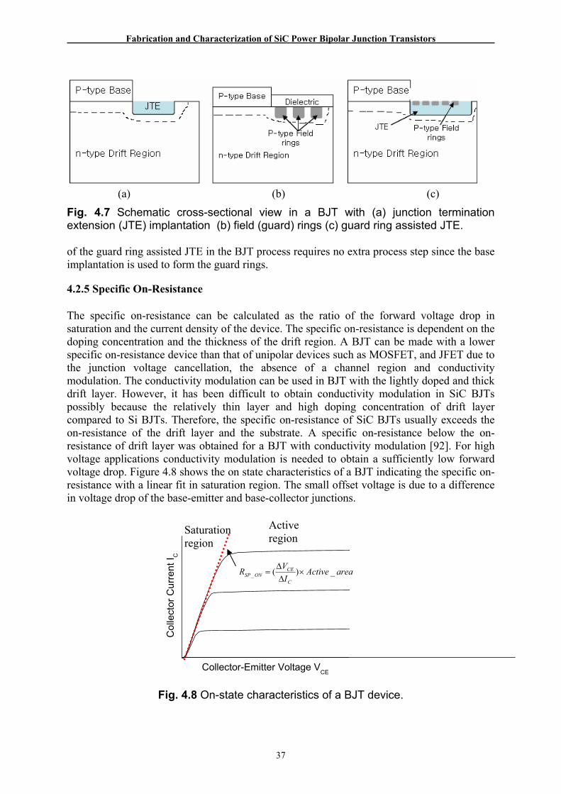
Fabrication and Characterization of SiC Power Bipolar Junction Transistors
37
(a) (b) (c)
Fig. 4.7 Schematic cross-sectional view in a BJT with (a) junction termination extension (JTE) implantation (b) field (guard) rings (c) guard ring assisted JTE. of the guard ring assisted JTE in the BJT process requires no extra process step since the base implantation is used to form the guard rings.
4.2.5 Specific On-Resistance The specific on-resistance can be calculated as the ratio of the forward voltage drop in saturation and the current density of the device. The specific on-resistance is dependent on the doping concentration and the thickness of the drift region. A BJT can be made with a lower specific on-resistance device than that of unipolar devices such as MOSFET, and JFET due to the junction voltage cancellation, the absence of a channel region and conductivity modulation. The conductivity modulation can be used in BJT with the lightly doped and thick drift layer. However, it has been difficult to obtain conductivity modulation in SiC BJTs possibly because the relatively thin layer and high doping concentration of drift layer compared to Si BJTs. Therefore, the specific on-resistance of SiC BJTs usually exceeds the on-resistance of the drift layer and the substrate. A specific on-resistance below the on-resistance of drift layer was obtained for a BJT with conductivity modulation [92]. For high voltage applications conductivity modulation is needed to obtain a sufficiently low forward voltage drop. Figure 4.8 shows the on state characteristics of a BJT indicating the specific on-resistance with a linear fit in saturation region. The small offset voltage is due to a difference in voltage drop of the base-emitter and base-collector junctions.
Fig. 4.8 On-state characteristics of a BJT device.
Col
lect
or C
urre
nt I C
Collector-Emitter Voltage VCE
areaActiveI
VRC
CEONSP _)(_ ×
ΔΔ
=
Saturation region
Active region

H.-S. LEE Chapter 4. Power Bipolar Junction Transistors in SiC
38
4.2.6 Mask Layout and Fabrication Process for SiC BJTs During the development of the SiC bipolar device process, more than seven batches have been fabricated using different designs of device and epitaxial layers, different processes (see Fig 4.9-4.14). A summary of design parameters for seven of the batches are presented in Table 4.4. A process flow for most batches is shown in Fig. 4.14.
Table 4.4 A summary of design parameters for the different BJT batches
Design parameter BJTs, 1st Batch BJTs, 2nd Batch BJTs, 3rd Batch Emitter
Doping (cm-3) 9·1019 6·1019 1.1·1019,T
5·1019 1·1019,T
Thickness (μm) 0.3 0.6 0.6 Base
Doping (cm-3) 1017-1018,G 2.4·1017 3·1017 Thickness (μm) 0.4 0.5 0.6 Extrinsic layer 4·1020 - -
Collector Doping (cm-3) 5·1015 4·1015 4·1015
Thickness (μm) 6 15 5 Highest Current
gain β 15 64 62
BVCEO (V) 1000 1100 < 400 V *
Specific on-resistance
(mΩcm2) 25.3 37.6 45.9 #
Layout
Device area (including contact pad)
300 μm × 300 μm, 600 μm × 600 μm,
1200 μm × 1450 μm
300 μm × 300 μm, 600 μm × 600 μm,
1200 μm × 1450 μm
300 μm × 300 μm, 600 μm × 600 μm,
1200 μm × 1450 μm
Note Epitaxially
Regrown Base
First continuous Epitaxial growth of collector, base, and
Emitter
Different types of passivation test
Entire mask Fig. 4.9 Fig. 4.9 Fig. 4.9 Paper VI IV II
* Devices without JTE G Graded base doping T Two step emitter layer
# Devices without contact annealing

Fabrication and Characterization of SiC Power Bipolar Junction Transistors
39
Table 4.4 A summary of design parameters for the different batches (Cont.)
BJTs, 4th Batch BJTs, 5th Batch BJTs, 6th Batch BJTs, 7th Batch
5·1019 1·1019,T
5·1019 0.8·1019,T
5·1019 1.5·1019,T
5·1019 1.5·1019,T
0.8 1 1 1.05
3.5·1017 (graded) 1·1017-4·1017,G 4·1017,G 4·1017,G 0.55 0.4 0.7 0.8
- - - 1.1·1019
4·1015 4·1015 4·1015 4·1015 15 15 5 5
30 35 60 42
500 400 1200 1800
15.4 9.9 5.2 9
300 μm × 300 μm,
1000 μm × 1000 μm, 2500 μm × 2500 μm
300 μm × 300 μm, 1000 μm × 1000 μm, 2500 μm × 2500 μm
300 μm × 300 μm, 1800 μm × 1800 μm 2050 μm × 2050 μm
300 μm × 300 μm, 1800 μm × 1800 μm2050 μm × 2050 μm
Base Ohmic contact with Ni/Ti/Al
1) 4o-off axis substrate
2) Al Overlayer metallization
1) N2O passivation layers.
2) Guard rings assisted JTE.
1) Regrown extrinsic base
2) Etched JTE
Fig. 4.11 Fig. 4.11 Fig. 4.13 Fig. 4.13 III V I,VII, and VIII IX
* Devices without JTE G Graded base doping T Two step emitter layer # Devices without contact annealing

H.-S. LEE Chapter 4. Power Bipolar Junction Transistors in SiC
40
The 1st batch (paper VI) design used an extrinsic base layer that was fabricated using epitaxial regrowth. This regrowth is an interesting alternative to a base contact implantation. The use of regrowth allows a shorter distance between the emitter edge and the extrinsic base than when using a base contact implant which creates more carrier lifetime reducing defects. The maximum current gain of these BJTs was around 6. It was, however, found that the regrown region was difficult to remove from the emitter edge by etching since the epitaxial growth on the emitter side-wall was significantly faster than on the flat surfaces. In the 2nd batch (paper IV), a continuous growth of the base-emitter junction was used to reduce the defect concentrations at the base-emitter interface. Another design characteristic of this batch was that the emitter was grown as a two-layer structure. This is efficient to improve the emitter injection efficiency by using a moderately high doping at the junction, while maintaining a good ohmic contact using a higher doping in the surface region. Also, Al base contact implantation was adapted in this batch and the base thickness was increased a little compared to earlier two batches for improving the breakdown voltage. Figure 4.10 shows the fabricated SiC BJTs with a 20 μm emitter width after metallization. The effect of the different types of passivation layers on the current gain of SiC BJTs has been investigated in the 3rd batch (Paper II). Three passivations have been used for BJTs; thermal SiO2, plasma deposited SiO2, and no passivation. To reduce other process effects, a simplified process was used without ion-implantation. In the 4th batch (paper III), SiC BJTs were fabricated with varying geometrical design in a new mask. Different emitter widths of 13, 10, 7, 5 and 3 μm were included in the new design (see Fig. 4.11). At the same time, different distances between the emitter edge and the base contact implant were used to see the influence of ion-implantation induced damage on the devices. Additionally, large area BJTs were also included in the mask; 1000 μm × 1000 μm and 2500 μm × 2500 μm. Ni/Ti/Al was used as base contact material to reduce the base contact resistance. Figure 4.12 shows the picture of the fabricated whole SiC wafer and a top view of a SEM Images. The collector, emitter, and base layers were epitaxially grown on the 4o-off axis SiC substrate. In this 5th batch (Paper V), a little higher base doping and thinner base width was used. To reduce the on-resistance, a thick Al overlayer was used. Also, for high current measurements the BJT was glued with silver epoxy on DCB substrate after dicing and Al wire bonding was performed between device and DCB substrate. However, the breakdown voltage was low around 400 V due to the punch through in the base layer. The base layer was measured by SIMS; doping and thicknesses were measured to 1·1017-4·1017 cm-3 and 0.4 μm. In the 6th batch (Paper I, VII, and VIII), the SiC BJTs have been fabricated with a passivation oxide grown in nitrous oxide (N2O) ambient to reduce the surface recombination. To understand the influence of improved passivation layers on the current gain in SiC BJTs, the current gain of SiC BJTs with conventional dry oxidation and otherwise the same process have been compared with the BJTs passivated in N2O ambient. The guard ring assisted JTE design has been included in the new mask. Also, large area BJTs of 1800 μm × 1800 μm and 2050 μm × 2050 μm were successfully fabricated in this batch (see Fig.4.13). In the 7th batch (Paper IX), the SiC BJTs with a regrown extrinsic base layer and an etched junction termination extension (JTE) has been fabricated. The p+ regrown layer BJT has the advantage of lower base contact resistivity and that the current gain becomes less sensitive to

Fabrication and Characterization of SiC Power Bipolar Junction Transistors
41
the distance between the emitter edge and the base contact compared to a BJT with ion-implantated base. Fabrication of BJTs without ion implantation means less lifetime-reducing defects and in addition, the surface morphology is improved since high-temperature annealing becomes obsolete.
Fig. 4.9 The layout of (a) the entire mask layout batch for the 1st 2nd and 3rd batches (b) the BJTs with different emitter widths of 5,10,20,30 μm and TLM structures.
Fig. 4.10 A SEM image of the fabricated 20 μm emitter width SiC BJT to the left, and a SEM image of the emitter and base contact of a BJT finger to the right.
(b)(a)
Emitter
Base

H.-S. LEE Chapter 4. Power Bipolar Junction Transistors in SiC
42
Fig. 4.11 The layout of (a) the entire mask layout batch for the 4th and 5th batches (b) the large area transistor with active area of 1 mm × 1 mm with guard rings. (c) BJTs with different emitter widths of 20,10, and 7 μm and TLM of emitter and base structures.
(a) (b)
Fig. 4.12 (a) A photo of a fabricated 4H-SiC BJTs on a 2 inch SiC wafer (b) A SEM image of the fabricated large area transistors.
(a) (b)
(c)
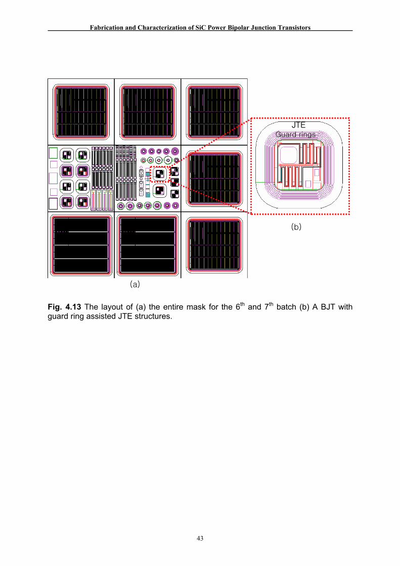
Fabrication and Characterization of SiC Power Bipolar Junction Transistors
43
Fig. 4.13 The layout of (a) the entire mask for the 6th and 7th batch (b) A BJT with guard ring assisted JTE structures.
JTE Guard rings
(a)
(b)
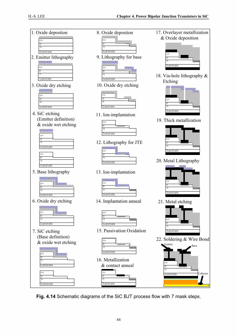
H.-S. LEE Chapter 4. Power Bipolar Junction Transistors in SiC
44
Fig. 4.14 Schematic diagrams of the SiC BJT process flow with 7 mask steps.
n+ p n
Substrate
Substrate
n+ p n
1. Oxide depostion
2. Emitter lithography
n+ p n
Substrate
3. Oxide dry etching
n+ p n
Substrate
n+ p n
Substrate
4. SiC etching (Emitter definition) & oxide wet etching
n+ p n
Substrate
n+ p n
Substrate
5. Base lithography
6. Oxide dry etching
n+ p n
Substrate
n+ p n
Substrate
7. SiC etching (Base definition) & oxide wet etching
n+ p n
Substrate
n+ p n
Substrate
8. Oxide depostion
n+ p n
Substrate
9. Lithography for base
n+ p n
Substrate
10. Oxide dry etching
11. Ion-implantation
n+ p n
Substrate
12. Lithography for JTE
n+ p n
Substrate
13. Ion-implantation
n+ p n
Substrate
14. Implantation anneal
n+ p n
Substrate
15. Passivation Oxidation
n+ p n
Substrate
16. Metallization & contact anneal
n+ p n
Substrate
17. Overlayer metallization & Oxide deposition
18. Via-hole lithography & Etching
n+ p n
Substrate
n+ p n
Substrate
19. Thick metallization
n+ p n
Substrate
20. Metal Lithography
n+ p n
Substrate
21. Metal etching
n+ p n
Substrate
Emitter Base
Collector
22. Soldering & Wire Bond

45
Chapter 5
SiC Power BJTs Results This chapter describes the results on the characteristics of the fabricated SiC Bipolar Junction Transistors (BJTs). The main emphasis is on the important factors of common emitter current gain, forward voltage drop, and breakdown voltage. In the following section, between 1200 V Si IGBT and 1200 V SiC BJT has been briefly compared. It will also be shown that other advantages including high voltage switching, high temperature and high current operating of SiC BJT have been investigated. Experimental details can be found in Table 4.4 pages 38-39 and appended papers.
5.1 Current Gain SiC BJTs As described before, to realize high performance SiC BJTs, the relatively low current gain is one important issue to be improved. A continuous growth of the base-emitter junction is useful to reduce the defect concentration and thus reduce the recombination current at the base-emitter interface compared to interrupted epitaxial growth. This continuous growth method has been introduced in the SiC BJT process (paper IV), and is believed to be important for achieving a high current gain. The schematic cross-sectional view and the top view of the fabricated 4H-SiC BJTs with 300 μm × 300 μm area is shown in Fig. 5.1.
Fig. 5.1 A microscopic image of a fabricated 4H-SiC BJT and schematic cross-section of the fabricated 4H-SiC BJT.
Emitter contact
N+ substrate Collector contact
15 μ m
700 n m
400 n m
200 n m
Base contact
ND= 5 × 1019 cm-3
ND= 7 × 1018 cm-3
NA= 3 × 1017 cm-3
ND= 4 × 1015 cm-3 NA≈ 7 × 1019 cm-3
Emitter
Base

H.-S. LEE Chapter 5. SiC Power BJTs Results
46
0 2 4 6 8 10 12 14
1E-7
1E-6
1E-5
1E-4
1E-3
0.01
0.1
Base Current IB
Cur
rent
I (A
)
Base-emitter Voltage VBE (V)
Collector Current IC β=(IC/IB)=64
(a) (b)
Fig. 5.2 (a) A measured gummel plot of a BJT with emitter width WE=20 μm, emitter length LE=1.13 mm and an area of 300 μm × 300 μm including contact pads.(b) Measured common emitter current gain β vs. IC for BJTs with LE=500 μm, WP+=5 μm and varying WE=10 μm, WE=20 μm and WE=30 μm. A clear emitter-size effect is distinguished.
The measured gummel plot of a typical 4H-SiC BJTs with emitter width WE=20 μm is shown in Fig. 5.2 (a). The base-emitter voltage (VBE) is swept from zero to a positive bias, while the collector-emitter voltage (VCE) is kept at a constant. A high current gain exceeding 60 is observed for the BJT at VBE=15 V. The common emitter current gain of SiC BJTs has been influenced by surface recombination (Paper IV). Figure 5.2 (b) displays measured current gain β vs. collector current IC at VCE=35 V for BJTs with three different emitter finger widths WE of 10, 20 and 30 μm. All three BJTs have an emitter finger length of 500 μm and the distance between the base-emitter junction and the base contact implant is 5 μm to avoid influence of ion implantation induced damage on the current gain. The current gain β clearly decreases with decreasing WE, as shown in Fig. 5.2 (b). This behaviour, commonly referred to as the emitter size effect [101] is caused by surface recombination that becomes more pronounced as the emitter area to periphery ratio decreases. The effects of surface recombination on the common-emitter current gain β can be described as in [101],
)11(2)(1EEC
Bsurf
C
InjScrBulk
LWJK
JJJJ
+⋅+++
=β
(5-1)
where JBulk(A·cm-2), JScr (A·cm-2) and JInj (A·cm-2) are the bulk recombination current density, the space-charge recombination current density, and the base-emitter back-injected current density, respectively. KBsurf (A·cm-1) is the surface recombination current divided by emitter periphery and WE and LE are the emitter width and the emitter length. The plot of JC/β versus (1/WE + 1/LE) should be straight line for a given collector current density JC.
0
10
20
30
40
50
60
70
80
0.001 0.01 0.1
WE=30 μm
WE=20 μm
WE=10 μm
Com
mon
em
itter
cur
rent
gai
n
Collector current IC (A)
VCE
=35 V

Fabrication and Characterization of SiC Power Bipolar Junction Transistors
47
Surface recombination which limits the current gain of 4H-SiC BJTs is also one important factor to be solved. An optimized passivation layer of 4H-SiC BJTs is a key issue to reduce the surface recombination current. In order to investigate how the electrical characteristics, especially the common emitter current gain of SiC BJTs depend on the passivation layer, 4H-SiC BJTs passivated by thermally grown oxide were compared with identical BJTs passivated by deposited SiO2 layers and unpassivated BJTs, as described in Paper II. Three different types of passivation layers were made in sequence with the same BJTs in this work. First, dry thermal oxidation at 1100 oC during five hours was carried out to obtain a standard passivation layer of the SiC BJTs. The thickness of the thermally grown oxide was 25 nm. After measuring the current gain, the thermally grown SiO2 was removed by buffered HF to create BJTs without passivation. After measuring the current gain, the BJTs were passivated by plasma enhanced chemical vapor deposition (PECVD) using a mixture of N2O and SiH4 gases in Ar atmosphere at a substrate temperature of 300 oC with an RF power of 300 W. The thickness of the deposited oxide was 200 nm. The measurement in Fig. 5.3 was performed 3 days after the oxide removal. It is likely that the gradual degradation in current gain for the device without passivation has been caused by the formation of a thin native oxide on the SiC surface. The current gain of devices with deposited oxide was severely decreased. The decrease is likely caused by defects or charge created during plasma deposition in and near the SiC/SiO2 interface in the emitter-base junction region. Apparently, the results lead to high possibility that optimization of the passivation layer is important for further improvement of the current gain of SiC BJTs, as shown in Paper II.
0,00 0,01 0,02 0,03 0,04 0,05 0,060
10
20
30
40
50
60
70
3 Days after the oxide removal
PECVD Oxide
Unpassivated
Dry Thermal Oxide
Com
mon
Em
itter
Cur
rent
Gai
n (β
)
Collector Current IC (A)
Fig. 5.3 Measured common emitter current gain β versus collector current IC for BJTs with passivation by thermally grown oxide, PECVD SiO2 and without passivation at room temperature. The BJTs have the emitter width WE=30 μm, emitter length LE=500 μm (b) JC/β versus 1/WE for the 30, 20, and 10 μm emitter width at JC=26.5 (A/cm2).
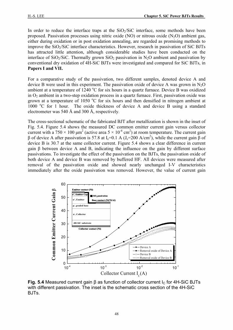
H.-S. LEE Chapter 5. SiC Power BJTs Results
48
In order to reduce the interface traps at the SiO2/SiC interface, some methods have been proposed. Passivation processes using nitric oxide (NO) or nitrous oxide (N2O) ambient gas, either during oxidation or in post oxidation annealing, are regarded as promising methods to improve the SiO2/SiC interface characteristics. However, research in passivation of SiC BJTs has attracted little attention, although considerable studies have been conducted on the interface of SiO2/SiC. Thermally grown SiO2 passivation in N2O ambient and passivation by conventional dry oxidation of 4H-SiC BJTs were investigated and compared for SiC BJTs, in Papers I and VII. For a comparative study of the passivation, two different samples, denoted device A and device B were used in this experiment. The passivation oxide of device A was grown in N2O ambient at a temperature of 1240 oC for six hours in a quartz furnace. Device B was oxidized in O2 ambient in a two-step oxidation process in a quartz furnace. First, passivation oxide was grown at a temperature of 1050 oC for six hours and then densified in nitrogen ambient at 1000 oC for 1 hour. The oxide thickness of device A and device B using a standard electrometer was 540 Å and 300 Å, respectively. The cross-sectional schematic of the fabricated BJT after metallization is shown in the inset of Fig. 5.4. Figure 5.4 shows the measured DC common emitter current gain versus collector current with a 750 × 100 μm2 (active area 5 × 10⁻⁴ cm2) at room temperature. The current gain β of device A after passivation is 57.8 at Ic=0.1 A (Jc=200 A/cm2), while the current gain β of device B is 30.7 at the same collector current. Figure 5.4 shows a clear difference in current gain β between device A and B, indicating the influence on the gain by different surface passivations. To investigate the effect of the passivation on the BJTs, the passivation oxide of both device A and device B was removed by buffered HF. All devices were measured after removal of the passivation oxide and showed nearly unchanged I-V characteristics immediately after the oxide passivation was removed. However, the value of current gain
10-4 10-3 10-2 10-10
10
20
30
40
50
60
n+, Emitter Cap
n+, Emitter
p-, graded base
n-, Collector
4H-SiC substrate
Emitter contact (Ni)
Collector contact (Ni)
SiO2 passivation
Base contact (Ni/Ti/Al)
n+, Emitter Cap
n+, Emitter
p-, graded base
n-, Collector
4H-SiC substrate
Emitter contact (Ni)
Collector contact (Ni)
SiO2 passivation
Base contact (Ni/Ti/Al)
Com
mon
Em
itter
Cur
rent
Gai
n β
Collector Current IC(A)
Device A Removal oxide of Device A Device B Removal oxide of Device B
Fig. 5.4 Measured current gain β as function of collector current IC for 4H-SiC BJTs with different passivation. The inset is the schematic cross section of the 4H-SiC BJTs.

Fabrication and Characterization of SiC Power Bipolar Junction Transistors
49
decreased as time increased, while the characteristics of devices A and B with passivation did not change during 3 months in air. The current gain of devices A and B after passivation removal is 26.7 and 26.1, respectively, as shown in Paper VII. The similar current gain of devices A and B after passivation removal indicates that the device A and B have very similar base and emitter epi-structures and material quality and fabrication processes, except for the oxide passivation.
10-3 10-2 10-10
10
20
30
40
50
60
Device B
Com
mon
Em
itter
Cur
rent
Gai
n β
Collector Current IC(A)
WE= 20 μm WE= 15 μm WE= 10 μm
VCE= 11 V
Device A
Fig. 5.5 Measured common emitter current gain β versus collector current IC for BJTs passivated by thermal oxidation in N2O ambient and for BJTs passivated by conventional dry thermal oxidation with emitter length (LE) =500 μm, and emitter widths WE = 20, 15, and 10 μm, respectively.
0.05 0.06 0.07 0.08 0.09 0.10 0.110
1
2
3
4
5
6
7
JC=160 A/cm2
J C/β
(A/c
m2 )
1/W E+1/LE (μm-1)
Device A Device B
JC=40 A/cm2
(a)
Fig. 5.6 Measured JC/β as a function of (1/WE + 1/LE) for device A and device B at Jc=40 A/cm2
and Jc=160 A/cm2varies from 10 to 20 μm and LE is 500 μm.

H.-S. LEE Chapter 5. SiC Power BJTs Results
50
Figure 5.5 shows the measured β versus IC for BJTs with the passivation oxide grown in N2O ambient and for the BJT with conventional dry oxidation, according to Paper I. The emitter width WE=20, 15, and 10 μm has been varied for both types of passivations. The peak current gain of the BJTs with the passivation grown in N2O ambient is about 2 times higher than for the BJTs with passivation by conventional dry thermal oxidation. It is clear that the current gain increases with large emitter width for BJTs with both types of passivation layers. Figure 5.6 shows a comparisons of JC/β versus (1/WE +1/LE) for Device A and B with emitter sizes of 20, 15, 10 μm at the collector current density JC = 40 A/cm2 and JC = 160 A/cm2. The slope of device A in Fig. 5.6 is negligible compared to that of device B. In other words, this figure indicates that the current gain of device A is less sensitive to the emitter size than that of device B. This reduced emitter size effect is consistent with a reduced surface recombination current at the edge of the base-emitter junction. The enhanced current gain and the reduced emitter size effect indicate that the passivation by thermal oxidation in N2O ambient can reduce the surface recombination in SiC BJTs.
5.2 Forward Voltage Drop
In order to develop high performance SiC BJTs taking full advantages of the material properties, formation of the p-type base Ohmic contact is one important processing issue. In general, a sufficiently low base resistance is necessary to obtain a low forward voltage drop in a SiC BJT, and the base contact resistance can be a significant part of the base resistance. It has been investigated how the electrical characteristics, in terms of specific on-resistance and common emitter current gain of SiC BJTs depend on the base contact resistance, according to Paper V.
(a) (b) Fig. 5.7 (a) The I-V characteristics of Ni/Ti/Al base contacts for as-deposited and after RTA annealing at 700 oC for 2 min and at 800 oC for 2 min. (b) Room temperature on-state characteristics of the BJTs with as-deposited base contact, after RTA contact annealing at 700 oC and 800 oC, and with overlayer metal Al/TiW after contact annealing.
-4 -3 -2 -1 0 1 2 3 4
-600,0µ
-400,0µ
-200,0µ
0,0
200,0µ
400,0µ
600,0µ
as deposited Base contact annealing at 700 oC for 2min Base contact annealing at 800 oC for 2min
Voltage (V)
Cur
rent
(A)
0 2 4 6 8 100,00
0,01
0,02
0,03
0,04
0,05
0,06
0,07
0,08
0,09
0,10
0,11
0,12
0,13
0,14
IB=0.5 mA/step
Col
lect
or C
urre
nt I C (A
)
Collector-Emitter Voltage VCE (V)
as deposited Base contact annealing at 700 oC for 2min Base contact annealing at 800 oC for 2min with Al/TiW overlayer metal after contact annealing

Fabrication and Characterization of SiC Power Bipolar Junction Transistors
51
Fig. 5.7 (a) shows the I-V characteristics of the Ni/Ti/Al base contacts before and after the annealing processes. While the base contact annealed at 700 oC for 2 min shows a non-ohmic behaviour, the current-voltage (I-V) characteristic for the contact annealed at 800 oC for 2 min shows a clear ohmic behaviour. The base contact resistivity, as measured with TLM, was 1.8 × 10⁻⁴ Ωcm2 after annealing at 800 oC for 2 min. The on-state characteristics of SiC BJTs with an active device area of 0.04 mm2 were investigated at room temperature for base contact annealing at different temperatures, as shown in Fig. 5.7 (b). A collector-emitter voltage drop of 3.9 V at a forward collector current of 50 mA (JC = 116 A/cm2) was observed for the as-deposited base contact. However, the voltage drop at the same current after base contact annealing at 700 oC and 800 oC was measured to 3.5 V and 1.3 V, respectively. This result indicates that the base ohmic contact plays a crucial role for the on-state characteristics of SiC BJTs (Paper V). Ion-implantation is normally used to increase the local surface doping concentration below the base contact, and this is referred to as a base contact implantation. However, high implantation doses are needed and this creates defects that can reduce the current gain because a substantial reduction of the carrier lifetime in the implanted region, as shown in Papers III and Paper IV. It is desirable for the practical fabrication of SiC BJTs to select a p-type contact metal, which can form a low-resistive ohmic contact to a lowly doped layer. The Ni/Ti/Al Ohmic contacts were formed on lowly doped p-type 4H-SiC with RTA (Paper VIII). Figure 5.8 shows the I-V characteristics of the Ni/Ti/Al contacts on p-type SiC measured between LTLM pad spacing of 5 μm before and after annealing at different temperatures of 700 and 800 oC. It showed perfect Ohmic behavior after RTP anneal at 800 oC, even though the contact resistivity on the lowly doped p-type region (~ 4 × 1017 cm-3) was relatively high (1.9 × 10⁻³ Ωcm2), while the contact resistivity with ion-implanted base region was 1.3 × 10⁻⁴ Ωcm2 after annealing at 800 oC.
-5 -4 -3 -2 -1 0 1 2 3 4 5-1.5
-1.0
-0.5
0.0
0.5
1.0
1.5
P-type epilayer4H-SiC Substrate (n+)
5 μm 10 μm 15 μm 20 μm 25 μm
P-type epilayer4H-SiC Substrate (n+)
Ni/Ti/Al contact
5 μm 10 μm 15 μm 20 μm 25 μm
P-type epilayer4H-SiC Substrate (n+)
5 μm 10 μm 15 μm 20 μm 25 μm
P-type epilayer4H-SiC Substrate (n+)
Ni/Ti/Al contact
5 μm 10 μm 15 μm 20 μm 25 μmCur
rent
(mA)
Voltage (V)
as-deposited 700 oC without implantation 800 oC without implantation 800 oC with implantation
Fig. 5.8 I-V characteristics of as-deposited and annealed Ni/Ti/Al contacts on SiC formed on an lowly doped epitaxial layer with doping concentration of 4 × 1017 cm-3 and an ion-implanted layer with a total dose of 2 × 1014 cm-2. The inset is a cross-sectional view of the linear TLM structures.

H.-S. LEE Chapter 5. SiC Power BJTs Results
52
Figure 5.9 displays on-state characteristics of the fabricated BJTs with and without ion-implantation. For a BJT with ion-implantation, a collector-emitter forward voltage drop of 0.44 for a forward collector current of 3.24 A (JC=100 A/cm2) has been observed at 25 oC. The forward voltage depends to a large extent on the collector resistance. For a BJT without ion-implantation, the forward voltage drop was 0.47 V at JC=100 A/cm2 at 25 oC. SiC power BJTs can be fabricated without base contact implantation with less than 10 % increase of VCE compared to a BJT with base contact implantation. This is a result of the successful formation of low-resistive Ni/Ti/Al Ohmic contacts to the lowly doped p-type base (Paper VIII).
0 1 2 3 4 50
2
4
6
8
10
12
14
16
18
20
22
0.47 V @ 100 A/cm2
Col
lect
or C
urre
nt I C
(A)
Collector-Emitter Voltage VCE (V)
Without ion-implantation With Ion-implantation IB=50mA/step
0.44 V @ 100 A/cm2
25 oC
Fig. 5.9 On-state characteristics at 25 oC for the BJTs with and without base contact ion-implantation.
1 2 3
0.4
0.5
0.6
0.7
0.8
0.9
1.0
Emittern+p
nSubstrate
Base
Collector
Wp+
Emittern+p
nSubstrate
Base
Collector
Wp+n+p
nSubstrate
Base
Collector
Wp+
Emitter-base distance Wp+ (μm)
Nor
mal
ized
cur
rent
gai
n β/
β max
Without ion-implantation With ion-implantation
Fig. 5.10 Normalized common emitter current gain versus distance (Wp+) between the emitter edge and the base contact implant or the base contact for the BJTs without implantation. The inset shows the cross-sectional view of SiC BJT including Wp+.

Fabrication and Characterization of SiC Power Bipolar Junction Transistors
53
SiC BJTs without base contact implantation can be fabricated without a significant current gain reduction as the distance to the base contact Wp+ decreases. Figure 5.10 shows a comparison of normalized current gain at IC=0.1 A (JC=200 A/cm2) with Wp+ in the range of 1-3 μm and a total area of 750 μm × 500 μm including contact pads. The SiC BJTs without base contact implantation have a constant current gain for Wp+ of 1 μm and larger, whereas the current gain of SiC BJTs with base contact implantation decreases significantly with 45 % as Wp+ is decreased from 3 μm to 1 μm. This result shows an additional advantage of avoiding the base contact implantation, since the extrinsic base region can be made shorter resulting in a lower base resistance, without reducing the current gain, according to Paper VIII.
5.3 Breakdown Voltage A high breakdown voltage of a power SiC BJTs can be obtained using similar strategies for junction termination as in other SiC devices. Recently, an interesting study on the use of a guard ring assisted JTE structure to improve the breakdown voltage of SiC pn diodes was presented [100]. The combination of two kinds of high voltage junction termination methods was used. Inclusion of the guard ring assisted JTE in the BJT process requires no extra process step since the base implantation is used to form the guard rings, as described in Paper I. Fig. 5.11 shows a cross-sectional view and a top view of a fabricated BJT with a guard ring assisted JTE and an emitter finger width of 25 μm. A comparison of the average open base breakdown BVCEO for 7 BJTs with only JTE and for 7 BJTs with guard ring assisted JTE is shown in Table 5.1. As shown in Fig. 5.12, the maximum BVCEO for BJTs with only JTE and for BJT with guard rings assisted JTE was approximately 810 V and 1200 V, respectively. The BJTs with guard ring assisted JTE have about 50 % higher breakdown voltage than BJTs with only JTE. The results are in qualitative agreement with ref. [100], which reports higher breakdown voltage and a reduced sensitivity to the JTE dose for guard ring assisted JTEs.
Fig. 5.11 Schematic cross-section of the guard rings assisted JTE to the left and a fabricated SiC BJT with a guard ring assisted JTE to the right.
Collector contact (Ni)
ND = 4×1015 cm-3, 15 μm
N+, 4H-SiC
NA≈ 4×1017 cm-3 (graded), 700 nm
ND = 1.5×1019 cm-3, 900 nm
ND = 5×1019 cm-3,100 nm
Emitter contact (Ni)
JTEJTE
Base contact
(Ni/Ti/Al) P+ P+
WE
SiO2 Passivation Layer
P+P+
Guard ring assisted JTE

H.-S. LEE Chapter 5. SiC Power BJTs Results
54
Table 5.1 Average measured open base breakdown voltage of at least 7 BJTs of both single JTE structures and guard ring assisted JTE structures
Average BVCEO (V) Standard Deviation (V)
Single JTE + Guard Ring 1070 130 Single JTE 713 77
500 600 700 800 900 1000 1100 1200 1300 14000.0
0.2
0.4
0.6
0.8
1.0
1.2
1.4
1.6
1.8
Single JTE + Guard Rings
BVCEO = 1200 V
Cur
rent
I(m
A)
Voltage (V)
BVCEO = 810 V
Single JTE
Fig. 5.12 Breakdown characteristics of a 4H-SiC BJT (active area 0.04 mm2) in open base configuration with single JTE structure () and with guard ring assisted JTE structure ().
5.4 SiC BJT without Ion-Implantation
Most SiC BJTs have a structure including at least one ion-implantation step because increasing the doping density in the base layer is an efficient approach for lowering the base contact resistivity. However, SiC BJTs with ion-implantation often suffer from incomplete activations of dopants and defects from implantation damages even after high temperature annealing.
A highly doped extrinsic base is necessary for several reasons. Firstly, a high doping lowers the base contact resistivity, which is crucial for the on-resistance. Secondly, the resistivity of p-type SiC is quite high, as a result of the low hole mobility and incomplete dopant ionization, and this results in a high base resistance that causes an increased potential at the location of the base contact at high currents. The collector, base and a thin n+ emitter were all epitaxially grown as shown in Fig. 5.13(a), as described in Paper VI. Emitter and base fingers were defined by oxide masked dry etching of SiC in an inductively coupled plasma (ICP) system. Measurements during the process before the epitaxial regrowth (probing directly on SiC) showed a current gain of 15 even at 150 °C. However, the common emitter current gain was reduced to 6 after epitaxial regrowth and etching. The current gain reduction is presumably caused by a local reduction of the emitter efficiency where the highly doped p+ region is remaining at the emitter edge. many BJTs had a high reverse leakage current likely caused by an remaining p+ regrowth at the side-wall of the emitter is schematically illustrated as the spacer in Fig. 5.13(a). It can be seen that the slope of the spacer region varies with orientation in Fig. 5.13(b).

Fabrication and Characterization of SiC Power Bipolar Junction Transistors
55
(a) (b) Fig. 5.13 (a) Cross-section of the BJT device structure obtained from process simulation ISE-DIOS (b) AFM image of the BJT top surface before passivation and metallization.
Fig. 5.14 Process steps for forming a regrown extrinsic base by combining dry etching with thermal oxidation. (a) Nonselective regrowth of a p+ layer followed by deposition of a SiO2 mask. (b) Etch removal of unnecessary p+ regrowth. (c) Thermal oxidation for removal of remaining p+ layer on the etched emitter-base junction. (d) SiC BJT with a regrown p+ extrinsic base (e) SEM cross-sectional view after dry etching. The remaining p+ regrown layer at this unwanted region has been found in a previous study (Paper VI) and has been reported to influence the electrical characteristics in Paper VI, although the extrinsic base layer on the etched emitter-base junction was defined by a typical dry etching method. Therefore, the reduction of the remaining p+ regrown layer on the surface at emitter-base junction is a critical factor. The oxidation rate of a-face >< 0211 is higher than that of Si <0001> face [102]. This different thermal oxidation rate for different orientations plays a role in efficiently removing the remaining p+ regrowth layer at the edge of the base-emitter junction. In Paper IX, plasma deposited SiO2 on the highly p- doped extrinsic base was defined by Reactive Ion Etch (RIE), as shown in Fig. 5.14 (a). The p+ regrown layer is still remaining, in a spacer at the edge of
n+ p n Substrate
n+ p n
Substrate
n+ p n
Substrate
n+ p n Substrate
P+ extrinsic base layer
SiO2 mask (a) (b)
(c) Thermal oxidation (d)
P+ extrinsic base layer
P+ extrinsic base layer
P+ regrown Base
P Base
N+ Emitter
(e)
Different Slope
N+ emitter, ND=9*1019 cm-3
P-base, graded 1017–1018 cm-3, 400 nm
N-collector, ND=5*1015 cm-3, 15 μm
P+ regrowth 4*1020cm-3
Emitter contact Base contact
SiO2 Spacer
N+ emitter, ND=9*1019 cm-3
P-base, graded 1017–1018 cm-3, 400 nm
N-collector, ND=5*1015 cm-3, 15 μm
P+ regrowth 4*1020cm-3
Emitter contact Base contact
SiO2 Spacer

H.-S. LEE Chapter 5. SiC Power BJTs Results
56
the emitter-base junction, as a result of the anisotropic inductively coupled plasma (ICP) etch (Fig. 5.14 (b)). To remove the remaining p+ regrowth, dry thermal oxidation at 1100 oC at 5 hours was performed as shown in Fig. 5.14 (c). After this, the oxide on the SiC BJT surface was removed in HF (Fig. 5.14 (d)) Figure 5.15 shows the top-view of a 1.8 mm × 1.8 mm SiC BJT without ion-implantation (active area =3.24 mm2 including metal pads). The maximum current gain of 42 was measured at Jc=258 A/cm2, VCE=3.7 V. The specific on-resistance is Rsp-On=9 mΩcm2. The relatively high specific on-resistance might result from an increased isolation trench depth [103] or from a poor backside collector contact. A stable and reproducible open base breakown of 1800 V was obtained, as shown in Fig. 5.16 and Paper IX.
Fig. 5.16 (a) Measured collector emitter current IC (A) vs. collector emitter voltage VCE (V) for the SiC BJT without ion implantation. (b) Measured open-base blocking characteristics for the SiC BJT without ion implantation.
600 800 1000 1200 1400 1600 1800 20000.0000
0.0005
0.0010
0.0015
0.0020
0.0025
Cur
rent
I (A
)
Collector-Emitter Voltage VCE (V)
BVCEO=1.8 kV
0 2 4 6 8 10 120
2
4
6
8
10
Col
lect
or C
urre
nt (A
)
Collector-Emitter Voltage VCE(V)
β=42Rsp_on= 9 mΩcm2
Ib=20 mA10 steps
(a) (b)
1.8 mm
1.8 mm
Base
Emitter
Base
Guard rings
Fig. 5.15 A top-view of a 1.8 mm × 1.8 mm active area fabricated SiC BJT without ion-implantation to the left and a SEM image of regrown structure to the right.
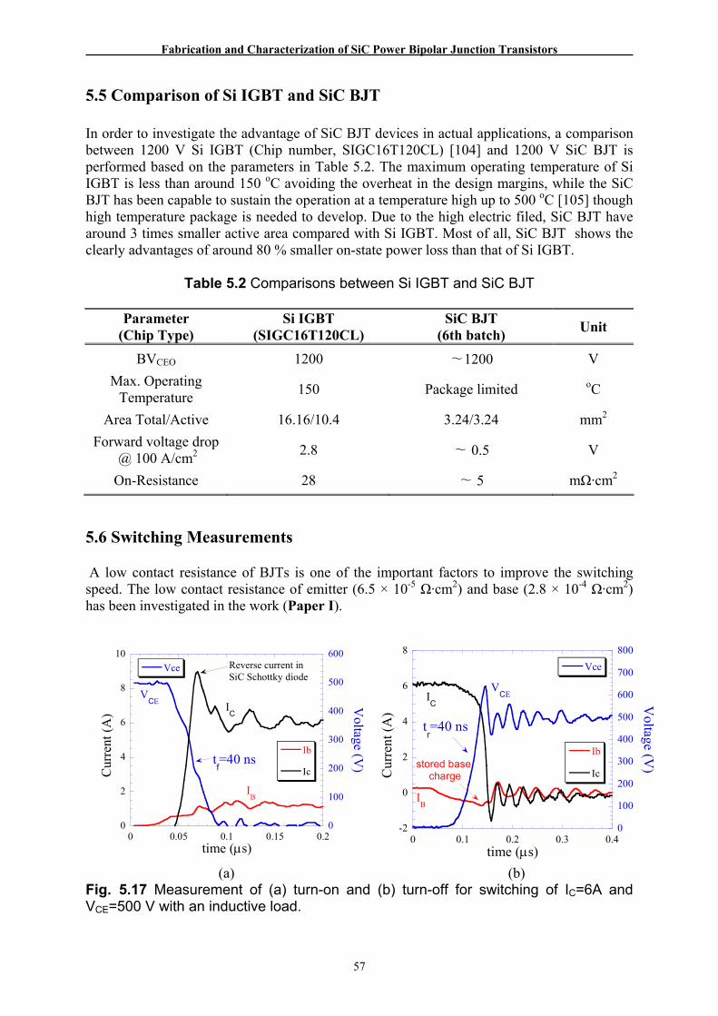
Fabrication and Characterization of SiC Power Bipolar Junction Transistors
57
5.5 Comparison of Si IGBT and SiC BJT In order to investigate the advantage of SiC BJT devices in actual applications, a comparison between 1200 V Si IGBT (Chip number, SIGC16T120CL) [104] and 1200 V SiC BJT is performed based on the parameters in Table 5.2. The maximum operating temperature of Si IGBT is less than around 150 oC avoiding the overheat in the design margins, while the SiC BJT has been capable to sustain the operation at a temperature high up to 500 oC [105] though high temperature package is needed to develop. Due to the high electric filed, SiC BJT have around 3 times smaller active area compared with Si IGBT. Most of all, SiC BJT shows the clearly advantages of around 80 % smaller on-state power loss than that of Si IGBT.
Table 5.2 Comparisons between Si IGBT and SiC BJT
Parameter (Chip Type)
Si IGBT (SIGC16T120CL)
SiC BJT (6th batch) Unit
BVCEO 1200 ∼1200 V Max. Operating
Temperature 150 Package limited oC
Area Total/Active 16.16/10.4 3.24/3.24 mm2 Forward voltage drop
@ 100 A/cm2 2.8 ∼ 0.5 V
On-Resistance 28 ∼ 5 mΩ·cm2
5.6 Switching Measurements A low contact resistance of BJTs is one of the important factors to improve the switching speed. The low contact resistance of emitter (6.5 × 10⁻⁵ Ω·cm2) and base (2.8 × 10⁻⁴ Ω·cm2) has been investigated in the work (Paper I).
(a) (b) Fig. 5.17 Measurement of (a) turn-on and (b) turn-off for switching of IC=6A and VCE=500 V with an inductive load.
0
2
4
6
8
10
0
100
200
300
400
500
600
0 0.05 0.1 0.15 0.2
Ib
Ic
Vce
Cur
rent
(A)
Voltage (V
)
time (μs)
IB
VCE I
C
tf=40 ns
Reverse current in SiC Schottky diode
-2
0
2
4
6
8
0
100
200
300
400
500
600
700
800
0 0.1 0.2 0.3 0.4
Ib
Ic
Vce
Cur
rent
(A)
Voltage (V
)
time (μs)
IB
VCEI
C
tr=40 ns
stored base charge
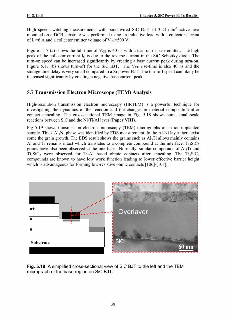
H.-S. LEE Chapter 5. SiC Power BJTs Results
58
High speed switching measurements with bond wired SiC BJTs of 3.24 mm2 active area mounted on a DCB substrate was performed using an inductive load with a collector current of IC=6 A and a collector emitter voltage of VCE=500 V. Figure 5.17 (a) shows the fall time of VCE is 40 ns with a turn-on of base-emitter. The high peak of the collector current IC is due to the reverse current in the SiC Schottky diode. The turn-on speed can be increased significantly by creating a base current peak during turn-on. Figure 5.17 (b) shows turn-off for the SiC BJT. The VCE rise-time is also 40 ns and the storage time delay is very small compared to a Si power BJT. The turn-off speed can likely be increased significantly by creating a negative base current peak.
5.7 Transmission Electron Microscope (TEM) Analysis High-resolution transmission electron microscopy (HRTEM) is a powerful technique for investigating the dynamics of the reaction and the changes in material composition after contact annealing. The cross-sectional TEM image in Fig. 5.18 shows some small-scale reactions between SiC and the Ni/Ti/Al layer (Paper VIII).
Fig 5.19 shows transmission electron microscopy (TEM) micrographs of an ion-implanted sample. Thick Al3Ni phase was identified by EDS measurement. In the Al3Ni layer there exist some the grain growth. The EDS result shows the grains such as Al3Ti alloys mainly contains Al and Ti remains intact which translates to a complete compound at the interface. Ti3SiC2 grains have also been observed at the interfaces. Normally, similar compounds of Al3Ti and Ti3SiC2 were observed for Ti-Al based ohmic contacts after annealing. The Ti3SiC2 compounds are known to have low work function leading to lower effective barrier height which is advantageous for forming low-resistive ohmic contacts [106]-[108].
Fig. 5.18 A simplified cross-sectional view of SiC BJT to the left and the TEM micrograph of the base region on SiC BJT.
n+
p
n
Substrate SiC
Overlayer
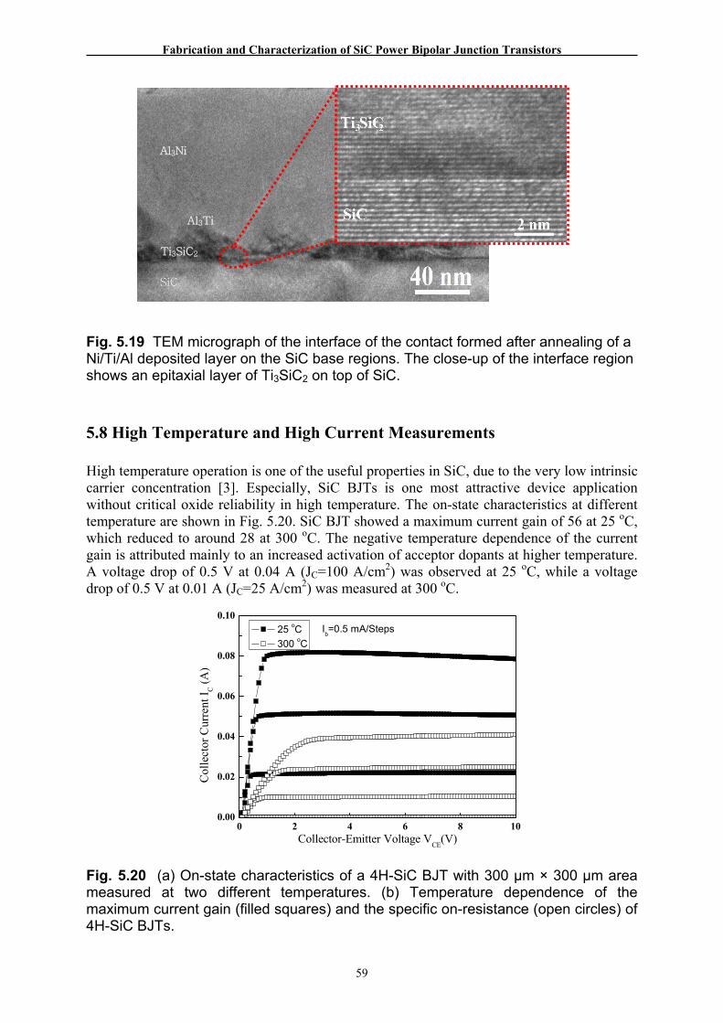
Fabrication and Characterization of SiC Power Bipolar Junction Transistors
59
Fig. 5.19 TEM micrograph of the interface of the contact formed after annealing of a Ni/Ti/Al deposited layer on the SiC base regions. The close-up of the interface region shows an epitaxial layer of Ti3SiC2 on top of SiC.
5.8 High Temperature and High Current Measurements High temperature operation is one of the useful properties in SiC, due to the very low intrinsic carrier concentration [3]. Especially, SiC BJTs is one most attractive device application without critical oxide reliability in high temperature. The on-state characteristics at different temperature are shown in Fig. 5.20. SiC BJT showed a maximum current gain of 56 at 25 oC, which reduced to around 28 at 300 oC. The negative temperature dependence of the current gain is attributed mainly to an increased activation of acceptor dopants at higher temperature. A voltage drop of 0.5 V at 0.04 A (JC=100 A/cm2) was observed at 25 oC, while a voltage drop of 0.5 V at 0.01 A (JC=25 A/cm2) was measured at 300 oC.
0 2 4 6 8 100.00
0.02
0.04
0.06
0.08
0.10
Col
lect
or C
urre
nt I C
(A)
Collector-Emitter Voltage VCE(V)
25 oC 300 oC
Ib=0.5 mA/Steps
Fig. 5.20 (a) On-state characteristics of a 4H-SiC BJT with 300 μm × 300 μm area measured at two different temperatures. (b) Temperature dependence of the maximum current gain (filled squares) and the specific on-resistance (open circles) of 4H-SiC BJTs.
SiC
Ti3SiC2
Al3Ti
Al3Ni

H.-S. LEE Chapter 5. SiC Power BJTs Results
60
SiC device can operable at temperatures as high as 500 oC in the probe-station environment, while the packaged devices can be found to allow operation in the range in the 200-250 oC due to the package limits. Thus, reliable packaging for SiC applications is necessary for high temperature operation. SiC can provide high current handling at high temperature. In Paper VIII, SiC BJT was glued with silver epoxy on DCB substrate after dicing and Al wire bonding was performed between device and DCB substrate (Fig. 5.21 (a)). This device was characterized using a Tektronix 371B curve tracer for high current measurement in pulsed mode (250 μs). Figure 5.21 (b) shows the collector current IC versus collector-emitter voltage VCE for different base currents at different temperature. For the BJT without implantation, VCE=0.44 V and VCE=0.82 V was measured at IC=3.24 A (JC=100 A/cm2) at 25 and 150 oC, respectively. The increase of the forward voltage drop VCE is due to the negative temperature dependence of the electron mobility that leads to an increasing collector resistance.
(a) (b)
Fig. 5.21 (a) A photo of a fabricated SiC 4H-SiC BJT glued with silver epoxy on DCB substrate with 1.8mm ×1.8mm (active area: 0.0324 cm2). (b) Measured IC versus VCE up to 19 A collector current (pulsed mode) for a BJT with WE=18 μm and an area of 1.8 mm × 1.8 mm including bonding pads at 25 oC
Base
Emitter 1.8 mm
DCB Substrate
1.8 mm
0 1 2 3 4 50
2
4
6
8
10
12
14
16
18
20
22
0.84 V @ 100 A/cm2
25 oC 150 oC
Col
lect
or C
urre
nt I C
(A)
Collectror-Emitter Voltage VCE (V)
IB=50mA/step
0.44 V @ 100 A/cm2

61
Chapter 6
Summary, Conclusions and Future Outlook The main objective of this thesis is the fabrication and characterization of SiC Bipolar junction Transistor (BJTs) for high power applications. The SiC BJT is an interesting switch with potential for very low on-state power losses for voltages in the range 600-2000V. The project was focused on developing and experimentally demonstrating power SiC BJTs. From several different batches, SiC BJTs were successfully fabricated and optimized to achieve state-of-the-art performance with a high current gain β ≈ 60, low on-resistance RSP_ON ≈ 5 mΩcm2 and high breakdown voltage BVCEO ≈ 1200 V.
SiC Process development:
To reduce the damage of device surface, inductively coupled plasma (ICP) etching with oxide mask was used. The oxide mask ICP etch resulted in a soft curved etch edge, while metal masks during dry etch can cause trenching effects. TEM measurements have revealed the advantages of the ICP etch. Also, the soft curved etched edge will likely have a positive influence on the junction termination. Even though 4o-off axis 4 inch SiC wafers are available in the market, 2-inch and 3-inch SiC wafers are still mainly used. At least 6-8 mask steps are needed in the SiC BJT fabrication. Therefore, a stable pattern transfer method such as stepper photolithography is advantageous to use. Photolithography with resolution and mask alignment accuracy well below 1 μm was enabled by using a g-line stepper with 2-inch SiC wafers mounted on a 4-inch Si carrier wafer. In order to avoid additional contact resistance power losses in SiC power BJTs, a low specific contact resistivity is required. Normally, to form ohmic contacts to p-type SiC requires high temperature post deposition annealing, typically in the range of 1000 oC, after metal deposition on heavily doped (≥1018 cm-3) surface. However, this procedure is not easy to adapt in to the SiC BJT process because high temperature anneal and high doping concentration of p-type base can negatively influence on electrical characterization. A low temperature anneal for the p-type Ni/Ti/Al contact n 4H-SiC has been demonstrated. A base contact resistivity of 1.3 × 10⁻⁴ Ωcm2 was demonstrated after low temperature anneal at 800 oC for 2 min. From a TEM study, Al3Ti and Ti3SiC2 compounds were identified. The
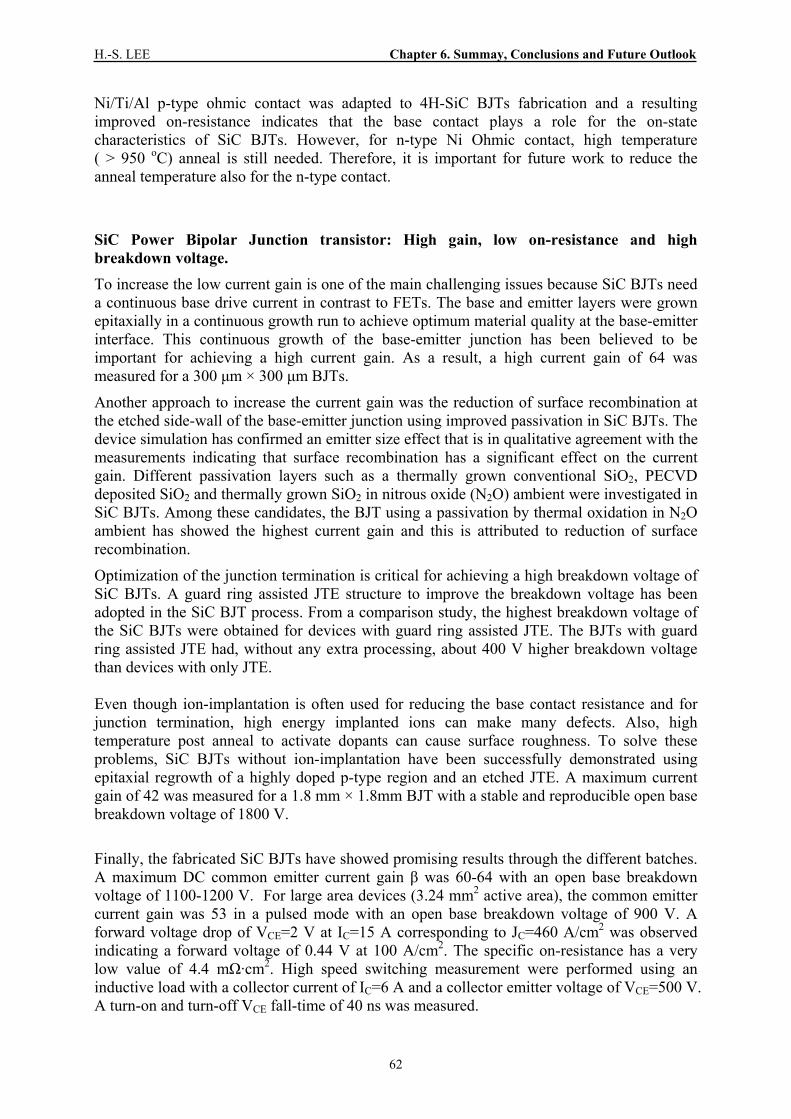
H.-S. LEE Chapter 6. Summay, Conclusions and Future Outlook
62
Ni/Ti/Al p-type ohmic contact was adapted to 4H-SiC BJTs fabrication and a resulting improved on-resistance indicates that the base contact plays a role for the on-state characteristics of SiC BJTs. However, for n-type Ni Ohmic contact, high temperature ( > 950 oC) anneal is still needed. Therefore, it is important for future work to reduce the anneal temperature also for the n-type contact.
SiC Power Bipolar Junction transistor: High gain, low on-resistance and high breakdown voltage. To increase the low current gain is one of the main challenging issues because SiC BJTs need a continuous base drive current in contrast to FETs. The base and emitter layers were grown epitaxially in a continuous growth run to achieve optimum material quality at the base-emitter interface. This continuous growth of the base-emitter junction has been believed to be important for achieving a high current gain. As a result, a high current gain of 64 was measured for a 300 μm × 300 μm BJTs.
Another approach to increase the current gain was the reduction of surface recombination at the etched side-wall of the base-emitter junction using improved passivation in SiC BJTs. The device simulation has confirmed an emitter size effect that is in qualitative agreement with the measurements indicating that surface recombination has a significant effect on the current gain. Different passivation layers such as a thermally grown conventional SiO2, PECVD deposited SiO2 and thermally grown SiO2 in nitrous oxide (N2O) ambient were investigated in SiC BJTs. Among these candidates, the BJT using a passivation by thermal oxidation in N2O ambient has showed the highest current gain and this is attributed to reduction of surface recombination.
Optimization of the junction termination is critical for achieving a high breakdown voltage of SiC BJTs. A guard ring assisted JTE structure to improve the breakdown voltage has been adopted in the SiC BJT process. From a comparison study, the highest breakdown voltage of the SiC BJTs were obtained for devices with guard ring assisted JTE. The BJTs with guard ring assisted JTE had, without any extra processing, about 400 V higher breakdown voltage than devices with only JTE. Even though ion-implantation is often used for reducing the base contact resistance and for junction termination, high energy implanted ions can make many defects. Also, high temperature post anneal to activate dopants can cause surface roughness. To solve these problems, SiC BJTs without ion-implantation have been successfully demonstrated using epitaxial regrowth of a highly doped p-type region and an etched JTE. A maximum current gain of 42 was measured for a 1.8 mm × 1.8mm BJT with a stable and reproducible open base breakdown voltage of 1800 V.
Finally, the fabricated SiC BJTs have showed promising results through the different batches. A maximum DC common emitter current gain β was 60-64 with an open base breakdown voltage of 1100-1200 V. For large area devices (3.24 mm2 active area), the common emitter current gain was 53 in a pulsed mode with an open base breakdown voltage of 900 V. A forward voltage drop of VCE=2 V at IC=15 A corresponding to JC=460 A/cm2 was observed indicating a forward voltage of 0.44 V at 100 A/cm2. The specific on-resistance has a very low value of 4.4 mΩ·cm2. High speed switching measurement were performed using an inductive load with a collector current of IC=6 A and a collector emitter voltage of VCE=500 V. A turn-on and turn-off VCE fall-time of 40 ns was measured.

Fabrication and Characterization of SiC Power Bipolar Junction Transistors
63
Future Outlook The SiC BJT is one of the promising power switching devices with low on-resistance, high breakdown voltage, and high temperature capability. A comparison between 1200 V Si IGBT and 1200 V SiC BJT shows the clearly advantages of around 80 % smaller on-state power loss, smaller size and higher operating temperature in a SiC BJT than that of Si IGBT. To successfully compete with Si MOSFETs and IGBTs, some technology development is needed. SiC devices can normally run at higher junction temperature than that of Si power devices. However, the packaging technology to reliably handle SiC devices operating over 200 oC is not perfectly developed yet. In order to use the high temperature capability of SiC devices, the packaging technology should be improved. Another issue of SiC devices is long-term stability. Recently, interesting work has been performed to reduce the degradation of SiC bipolar devices [109]-[110]. The stacking fault in the basal plane dislocation (BPD) is believed to be the most important defect that may cause bipolar degradation. Therefore, SiC devices fabricated on substrate with low BPD density will reduce the degradation of SiC devices. One new approach to reduce the degradation is to start with on-axis SiC substrate instead of off-axis substrate [110]. Summary We have shown in seven different batches that it is possible to produce SiC BJTs with high current gain β, low specific on-resistance RSP_ON, high breakdown voltage, high operating temperature together with high current handling capability and SiC BJT is a strong candidate to replace Si power devices.
Parameter SiC BJT Paper
Highest BVCEO 1800-1900 V IX
Highest Current Density 1049 A/cm2 (34 A) V Highest Operating
Temperature 300 oC (in probe environment)200 oC (in packaged device) V
Highest β 60-64 I and IV
Lowest RSP_ON 4.4-5 mΩ·cm2 I Forward voltage drop
@ 100 A/cm2 ∼ 0.5 V I
Fastest Switching Speed 40 ns I

H.-S. LEE Chapter 6. Summay, Conclusions and Future Outlook
64

65
Bibliography
[1] B. K. Bose, “Advances in power electronics-its impact on the environment,” presented at
IEEE International Symposium on Industrial Electronics. 7-10 July , Pretoria, South Africa,
1998.
[2] B. J. Baliga, “Power semiconductor device Figure of merit for high-frequency applications,”
IEEE Electron Device Letters, vol. 10, p. 455, 1989.
[3] C.-M. Zetterling, “Process technology for silicon carbide devices,” in EMIS processing
series, IEE, 2002.
[4] L. S. Ramsdell, “Studies on silicon carbide,” American Mineralogist, vol. 32, p. 64, 1947.
[5] S.-M. Koo, “Design and process issues of junction- and Ferroelectric- Field Effect
Transistors in Silicon Carbide,” Ph.D Thesis, KTH, Royal Institute of Technology, Sweden,
2003.
[6] E. Danielsson, “Processing and electrical characterization of GaN/SiC Heterojunctions and
SiC bipolar transistors,” Ph.D Thesis, KTH, Royal Institute of Technology, Sweden, 2001.
[7] T. P. Chow, “SiC and GaN high-voltage power switching devices,” Materials Science
Forum, vol. 338, p. 1155, 2000.
[8] B. J. Baliga, “Power Semiconductor Devices,” PWS publishing company, 1997.
[9] N. D. Arora, J. R. Hauser, and D. J. Roulston, “Electron and hole mobilities in silicon as a
function of concentration and temperature,” IEEE Transactions on Electron Devices, vol. 29,
p. 292, 1982.
[10] D. M. Caughey and R. E. Thomas, “Carrier mobilities in silicon empirically related to
doping and field,” Proceedings of the IEEE, vol. 55, p. 2192, 1967.
[11] T. Troffer, C. Peppermuller, G. Pensl, K. Rottner, and A. Schoner, “Phosphorus-related
donors in 6H-SiC generated by ion implantation,” Journal of Applied Physics, vol. 80,
p. 3739, 1996.
[12] T. Troffer, M. Schadt, T. Frank, H. Itoh, G. Pensl, J. Heindl, H. P. Strunk, and M. Maier,
“Doping of SiC by implantation of boron and aluminum,” Physica Status Solidi A, vol. 162,
p. 277, 1997.
[13] M. A. Capano, R. Santhakumar, R. Venugopal, M. R. Melloch, and J. A. Cooper, Jr.,
“Phosphorus implantation into 4H-silicon carbide,” Journal of Electronic Materials, vol. 29,
p. 210, 2000.

H.-S. LEE Bibliography
66
[14] R. N. Hall, “Electron-hole recombination in germanium,” Physical Review, vol. 87, p. 387,
1952.
[15] W. Shockley and W. T. Read, Jr., “Statistics of the recombinations of holes and electrons,”
Physical Review, vol. 87, p. 835, 1952.
[16] J. P. Bergman, O. Kordina, and E. Janzen, “Time resolved spectroscopy of defects in SiC,”
Physica Status Solidi A, vol. 162, p. 65, 1997.
[17] V. Grivickas, J. Linnros, A. Galeckas, and V. Bikbajevas, “Relevance of the exciton effect
on ambipolar transport and Auger recombination in silicon at room temperature,” in Proc.
ISPSD, 21-26 July, Berlin, Germany, 1996.
[18] A. Galeckas, J. Linnros, V. Grivickas, U. Lindefelt, and C. Hallin, “Auger recombination in
4H-SiC: unusual temperature behavior,” Applied Physics Letters, vol. 71, p. 3269, 1997.
[19] U. Lindefelt, “Doping-induced band edge displacements and band gap narrowing in 3C-, 4H-,
6H-SiC, and Si,” Journal of Applied Physics, vol. 84, p. 2628-37, 1998.
[20] Y. M. Tairov and V. F. Tsvetkov, “Aluminum-doped epitaxial SiC layers,” Inorganic
Materials, vol. 14, p. 1387, 1978.
[21] Cree.Inc., http://www.cree.com.
[22] SiCrystal.A.G., http://www.sicrystal.com.
[23] H. M. Hobgood, M. F. Brady, M. R. Calus, J. R. Jenny, R. T. Leonard, D. P. Malta, S. G.
Muller, A. R. Powell, V. F. Tsvetkov, R. C. Glass, and C. H. Carter Jr., “Silicon carbide
crystal and substrate technology: A survey of recent advances,” in Proc. ICSCRM, Oct 5-10,
Lyon, France, 2003.
[24] X. Zhang, S. Ha, M. Benamara, M. Skowronski, J. J. Sumakeris, S. Ryu, M. J. Paisley, and
M. J. O'Loughlin, “Structure of carrot defects in 4H-SiC epilayers,” Materials Science
Forum, vol. 527, p. 327, 2006.
[25] M. Syvajarvi, R. Yakimova, and E. Janzen, “Anisotropic etching of SiC,” Journal of the
Electrochemical Society, vol. 147, p. 3519, 2000.
[26] S. Dohmae, K. Shibahara, S. Nishino, and H. Matsunami, “Plasma etching of CVD grown
cubic SiC single crystals,” Japanese Journal of Applied Physics, Part 2 (Letters), vol. 24,
p. 873, 1985.
[27] R. Wolf and R. Helbig, “Reactive ion etching of 6H-SiC in SF6/O2 and CF4/ O2 with N2
additive for device fabrication,” Journal of the Electrochemical Society, vol. 143, p. 1037,
1996.
[28] P. H. Yih, V. Saxena, and A. J. Steckl, “A review of SiC reactive ion etching in fluorinated
plasmas,” Physica Status Solidi B, vol. 202, p. 605, 1997.

Fabrication and Characterization of SiC Power Bipolar Junction Transistors
67
[29] J. B. Casady, E. D. Luckowski, M. Bozack, D. Sheridan, R. W. Johnson, and J. R. Williams,
“Etching of 6H-SiC and 4H-SiC using NF3 in a reactive ion etching system,” Journal of the
Electrochemical Society, vol. 143, p. 1750, 1996.
[30] L. Jiang, N. O. V. Plank, M. A. Blauw, R. Cheung, and E. van der Drift, “Dry etching of SiC
in inductively coupled Cl2/Ar plasma,” Journal of Physics D (Applied Physics), vol. 37,
p. 1809, 2004.
[31] L. Jiang and R. Cheung, “Impact of Ar addition to inductively coupled plasma etching of
SiC in SF6/O2 “ presented at 29th International Conference on Micro and Nano Engineering,
22-25 Sept. 2003
[32] F. A. Khan and I. Adesida, “High rate etching of SiC using inductively coupled plasma
reactive ion etching in SF6 based gas mixtures,” Applied Physics Letters, vol. 75, p. 2268,
1999.
[33] J. R. Flemish and K. Xie, “Profile and morphology control during etching of SiC using
electron cyclotron resonant plasmas,” Journal of the Electrochemical Society, vol. 143,
p. 2620, 1996.
[34] R. Bogue, “Developments in advanced silicon etching techniques by STS Systems,” Sensor
Review, vol. 22, p. 41, 2002.
[35] Koo. S.-M., Lee.S.-K., Zetterling.C.-M., Östling.M., Forsberg.U., and E. Janzen, “Influence
of trenching effect on the characteristics of Buried-Gate SiC Junctio Field-Effect
Transistors,” Materials Science Forum, vol. 389-393, p. 1235, 2002.
[36] Y. Negoro, T. Kimoto, and H. Matsunami, “High-voltage 4H-SiC pn diodes fabricated by p-
type ion implantation,” Electronics and Communications in Japan, Part 2 (Electronics), vol.
86, p. 44, 2003.
[37] S.-K. Lee, C.-M. Zetterling, E. Danielsson, M. Östling, J.-P. Palmquist, H. Hogberg, and U.
Jansson, “Electrical characterization of TiC ohmic contacts to aluminum ion implanted 4H-
silicon carbide,” Applied Physics Letters, vol. 77, p. 1478, 2000.
[38] R. Nipoti, F. Moscatelli, A. Scorzoni, A. Poggi, G. C. Cardinali, M. Lazar, C. Raynaud, D.
Planson, M.-L. Locatelli, and J.-P. Chante, “Contact resistivity of Al/Ti ohmic contacts on p-
type ion implanted 4H- and 6H-SiC,” presented at Silicon Carbide 2002 - Materials,
Processing and Devices, Dec 2-4, Boston, MA, United States, 2002.
[39] S. Tanimoto, N. Kiritani, M. Hoshi, and H. Okushi, “Ohmic contact structure and fabrication
process applicable to practical SiC devices,” in Proc. ICSCRM, Oct 28-Nov 2 2001, Tsukuba,
Japan, 2001.
[40] A. Itoh, T. Kimoto, and H. Matsunami, “Excellent reverse blocking characteristics of high-
voltage 4H-SiC Schottky rectifiers with boron-implanted edge termination,” IEEE Electron
Device Letters, vol. 17, p. 139, 1996.

H.-S. LEE Bibliography
68
[41] D. Alok and B. J. Baliga, “SiC device edge termination using finite area argon implantation,”
IEEE Transactions on Electron Devices, vol. 44, p. 1013, 1997.
[42] K. V. Vassilevski, A. B. Horsfall, C. M. Johnson, and N. G. Wright, “Edge termination of
SiC Schottky diodes with guard rings formed by high energy boron implantation,” in Proc.
ICSCRM, Oct 5-10, Lyon, France, 2003.
[43] P. A. Losee, S. K. Balachandran, L. Zhu, C. Li, J. Seiler, T. P. Chow, I. B. Bhat, and R. J.
Gutmann, “High-voltage 4H-SiC PiN rectifiers with single-implant, multi-zone JTE
termination,” in Proc.16th ISPSD, 24-27 May, Kitakyushu, Japan, 2004.
[44] M. Rambach, A. J. Bauer, L. Frey, P. Friedrichs, and H. Ryssel, “Annealing of aluminum
implanted 4H-SiC: comparison of furnace and lamp annealing,” in Proc. ECSCRM, 31 Aug.-
4 Sept. 2004
[45] L. Ruppalt, S. Stafford, D. Yuan, R. Vispute, T. Venkatesan, R. Sharma, K. Jones, M. Ervin,
K. Kirchner, T. Zheleva, M. Wood, B. Geil, and E. Forsythe, “Using a PLD BN/AlN
composite as an annealing cap for ion implanted SiC,” presented at 2001 International
Semiconductor Device Research Symposium, 5-7 Dec., Washington, DC, USA, 2001.
[46] J. F. Ziegler, “Ion implantation science and technology,” Academic Press, 1984.
[47] Y. Song, S. Dhar, L. C. Feldman, G. Chung, and J. R. Williams, “Modified Deal Grove
model for the thermal oxidation of silicon carbide,” Journal of Applied Physics, vol. 95,
p. 4953, 2004.
[48] V. V. Afanasev, M. Bassler, G. Pensl, and M. Schulz, “Intrinsic SiC/SiO2 interface states,”
Physica Status Solidi (A) Applied Research, vol. 162, p. 321, 1997.
[49] L. A. Lipkin and J. W. Palmour, “Improved oxidation procedures for reduced SiO2/ SiC
defects,” presented at 37th Electronic Materials Conference. III-V Nitrides and Silicon
Carbide, 1995
[50] K. Ueno, R. Asai, and T. Tsuji, “4H-SiC MOSFET's utilizing the H2 surface cleaning
technique,” IEEE Electron Device Letters, vol. 19, p. 244, 1998.
[51] S. Sridevan and B. J. Baliga, “Inversion layer mobility in SiC MOSFETs,” presented at
Silicon Carbide, III-Nitrides and Related Materials., 31 Aug.-5 Sept. 1997
[52] R. Schorner, P. Friedrichs, D. Peters, D. Stephani, S. Dimitrijev, and P. Jamet, “Enhanced
channel mobility of 4H-SiC metal-oxide-semiconductor transistors fabricated with standard
polycrystalline silicon technology and gate-oxide nitridation,” Applied Physics Letters, vol.
80, p. 4253, 2002.
[53] G. Gudjonsson, H. O. Olafsson, and E. O. Sveinbjornsson, “Enhancement of inversion
channel mobility in 4H-SiC MOSFETs using a gate oxide grown in nitrous oxide (N2O),” in
Proc. ICSCRM, Oct 5-10, Lyon, France, 2003.
Fabrication and Characterization of SiC Power Bipolar Junction Transistors
69
[54] G. Y. Chung, C. C. Tin, J. R. Williams, J. K. McDonald, M. D. Ventra, S. T. Pantelides, L. C.
Feldman, and R. A. Weller, “Effect of nitric oxide annealing on the interface trap densities
near the band edges in the 4H polytype of silicon carbide,” Applied Physics Letters, vol. 76,
p. 1713, 2000.
[55] S.-K. Lee, C.-M. Zetterling, M. Östling, J.-P. Palmquist, H. Hoberg, and U. Jansson, “Low
resistivity ohmic titanium carbide contacts to n- and p-type 4H-silicon carbide,” Solid-State
Electronics, vol. 44, p. 1179, 2000.
[56] S. Liu, K. Reinhardt, C. Severt, and J. Scofield, “Thermally stable ohmic contacts on n-type
6H- and 4H-SiC based on silicide and carbide,” in Proc. ICSCRM, 18-21 Sept., Kyoto, Japan,
1995.
[57] E. D. Luckowski, J. M. Delucca, J. R. Williams, S. E. Mohney, M. J. Bozack, T. Isaacs-
Smith, and J. Crofton, “Improved ohmic contact to n-type 4H and 6H-SiC using nichrome,”
presented at III-V Nitrides and Silicon Carbide, 1997.
[58] L. G. Fursin, J. H. Zhao, and M. Weiner, “Nickel ohmic contacts to p and n-type 4H-SiC,”
Electronics Letters, vol. 37, p. 1092, 2001.
[59] N. Lundberg and M. Östling, “CoSi2 ohmic contacts to n-type 6H-SiC,” Solid-State
Electronics, vol. 38, p. 2023, 1995.
[60] S.-K. Lee, S.-M. Koo, C.-M. Zetterling, and M. Östling, “Ohmic contact formation on
inductively coupled plasma etched 4H-silicon carbide,” presented at III-V Nitrides and
Silicon Carbide Materials and Devices, 27-29 June, 2001
[61] N. A. Papanicolaou, A. Edwards, M. V. Rao, and W. T. Anderson, “Si/Pt Ohmic contacts to
p-type 4H-SiC,” Applied Physics Letters, vol. 73, p. 2009, 1998.
[62] Lin, J.Y., Mohney, S.E., Smalley, M., Crofton, J., Williams, J.R., and Isaacs-Smith, T.,
“Engineering the Al-Ti/p-SiC ohmic contact for improved performance,” Materials
Research Society Symposium Proceedings, vol. 640, pp. H7.3.1, 2001.
[63] Y. Sugawara, D. Takayama, K. Asano, R. Singh, J. Palmour, and T. Hayashi, “12-19 kV 4H-
SiC pin diodes with low power loss,” in Proc. ISPSD, 4-7 June, Osaka, Japan, 2001.
[64] M. Östling, H.-S. Lee, M. Domeij, and C.-M. Zetterling, “Silicon carbide devices and
processes - present status and future perspective,” presented at Proceedings of the
International Conference on Mixed Design of Integrated Circuits and Systems, 22-24 June,
Gdynia, Poland, 2006.
[65] J. Tan, J. A. Cooper, Jr., and M. R. Melloch, “High-voltage accumulation-layer UMOSFET's
in 4H-SiC,” IEEE Electron Device Letters, vol. 19, p. 487, 1998.
[66] S.-H. Ryu, S. Krishnaswami, M. O'Loughlin, J. Richmond, A. Agarwal, J. Palmour, and A.
R. Hefner, “10-kV, 123-mΩcm2 4H-SiC power DMOSFETs,” IEEE Electron Device Letters,
vol. 25, p. 556, 2004.
H.-S. LEE Bibliography
70
[67] D. Peters, R. Schorner, P. Friedrichs, J. Volkl, H. Mitlehner, and D. Stephani, “An 1800 V
triple implanted vertical 6H-SiC MOSFET,” IEEE Transactions on Electron Devices, vol. 46,
p. 542, 1999.
[68] J. H. Zhao, K. Tone, P. Alexandrov, L. Fursin, and M. Weiner, “1710-V 2.77 mΩcm2 4H-
SiC trenched and implanted vertical junction field-effect transistors,” IEEE Electron Device
Letters, vol. 24, p. 81, 2003.
[69] J. B. Fedison, N. Ramungul, T. P. Chow, M. Ghezzo, and J. W. Kretchmer, “Electrical
characteristics of 4.5 kV implanted anode 4H-SiC p-i-n junction rectifiers,” IEEE Electron
Device Letters, vol. 22, p. 130, 2001.
[70] J. H. Zhao, P. Alexandrov, and X. Li, “Demonstration of the first 10-kV 4H-SiC Schottky
barrier diodes,” IEEE Electron Device Letters, vol. 24, p. 402, 2003.
[71] T. Nakamura, T. Miyanagi, I. Kamata, T. Jikimoto, and H. Tsuchida, “A 4.15 kV 9.07
mΩcm2 4H-SiC Schottky-barrier diode using Mo contact annealed at high temperature,”
IEEE Electron Device Letters, vol. 26, p. 99, 2005.
[72] H. M. McGlothlin, D. T. Morisette, J. A. Cooper, Jr., and M. R. Melloch, “4 kV silicon
carbide Schottky diodes for high-frequency switching applications,” presented at 1999 57th
Annual Device Research Conference Digest, 28-30 June, Santa Barbara, CA, USA, 1999.
[73] F. Dahlquist, J.-O. Svedberg, C.-M. Zetterling, M. Östling, B. Breitholtz, and H.
Lendenmann, “A 2.8 kV, forward drop JBS diode with low leakage,” in Proc. ICSCRM, 10-
15 Oct. 1999
[74] L. Zhu, T. P. Chow, K. A. Jones, and A. Agarwal, “Design, fabrication, and characterization
of low forward drop, low leakage, 1-kV 4H-SiC JBS rectifiers,” IEEE Transactions on
Electron Devices, vol. 53, p. 363, 2006.
[75] Y. Li, J. A. J. Cooper, and M. A. Capano, “High-voltage (3 kV) UMOSFETs in 4H-SiC,”
IEEE Transactions on Electron Devices, vol. 49, p. 972, 2002.
[76] Y. Sui, T. Tsuji, and J. A. Cooper, Jr., “On-State Characteristics of SiC power UMOSFETs
on 115-μm drift Layers,” IEEE Electron Device Letters, vol. 26, p. 255, 2005.
[77] S.-H. Ryu, A. Agarwal, J. Richmond, M. Das, L. Lipkin, J. Palmour, N. Saks, and J.
Williams, “Large-area (3.3 mm ×3.3 mm) power MOSFETs in 4H-SiC,” in Proc. ICSCRM,
28 Oct.-2 Nov. 2001
[78] S.-H. Ryu, S. Krishnaswami, M. Das, B. Hull, J. Richmond, B. Heath, A. Agarwal, J.
Palmour, and J. Scofield, “10.3 mΩcm2, 2 kV power DMOSFETs in 4H-SiC,” in Proc.
ISPSD, 23-26 May, Santa Barbara, CA, USA, 2005.
[79] P. Friedrichs, H. Mitlehner, R. Schorner, K.-O. Dohnke, R. Elpelt, and D. Stephani,
“Application-oriented unipolar switching SiC devices,” in Proc. ICSCRM, 28 Oct.-2 Nov.
2001

Fabrication and Characterization of SiC Power Bipolar Junction Transistors
71
[80] H. Onose, A. Watanabe, T. Someya, and Y. Kobayashi, “2 kV 4H-SiC junction FETs,” in
Proc. ICSCRM, 28 Oct.-2 Nov. 2001
[81] J. H. Zhao, P. Alexandrov, J. Zhang, and X. Li, “Fabrication and characterization of 11-kV
normally off 4H-SiC trenched-and-implanted vertical junction FET,” IEEE Electron Device
Letters, vol. 25, p. 474, 2004.
[82] K. Asano, Y. Sugawara, S. Ryu, R. Singh, J. Palmour, T. Hayashi, and D. Takayama, “5.5
kV normally-off low RonS 4H-SiC SEJFET,” in Proc. ISPSD, Osaka, Japan, 2001.
[83] T. McNutt, V. Veliadis, E. Stewart, H. Hearne, J. Reichl, P. Oda, S. Van Campen, J. Ostop,
and C. R. Clarke, “Silicon carbide JFET cascode switch for power conditioning
applications,” presented at IEEE Vehicle Power and Propulsion Conference, 7-9 Sept.,
Chicago, IL, USA, 2005.
[84] S.-H. Ryu, A. K. Agarwal, R. Singh, and J. W. Palmour, “1800 V NPN bipolar junction
transistors in 4H-SiC,” IEEE Electron Device Letters, vol. 22, p. 124, 2001.
[85] C.-F. Huang and J. A. Cooper Jr., “4H-SiC npn bipolar junction transistors with BVCEO;
3,200 V,” in Proc. ISPSD, Jun 4-7, Santa Fe, NM, United States, 2002.
[86] Y. Luo, J. Zhang, P. Alexandrov, L. Fursin, J. H. Zhao, and T. Burke, “High Voltage (< 1
kV) and High Current Gain (32) 4H-SiC Power BJTs Using Al-Free Ohmic Contact to the
Base,” IEEE Electron Device Letters, vol. 24, p. 695, 2003.
[87] J. Zhang, J. H. Zhao, P. Alexandrov, and T. Burke, “Demonstration of first 9.2 kV 4H-SiC
bipolar junction transistor,” Electronics Letters, vol. 40, p. 1381, 2004.
[88] S. Balachandran, T. P. Chow, A. Agarwal, C. Scozzie, and K. A. Jones, “4 kV 4H-SiC
epitaxial emitter bipolar junction transistors,” IEEE Electron Device Letters, vol. 26, p. 470,
2005.
[89] S. Krishnaswami, A. Agarwal, S.-H. Ryu, C. Capell, J. Richmond, J. Palmour, S.
Balachandran, T. P. Chow, S. Bayne, B. Geil, K. Jones, and C. Scozzie, “1000-V, 30-A 4H-
SiC BJTs with high current gain,” IEEE Electron Device Letters, vol. 26, p. 175, 2005.
[90] J. Zhang, P. Alexandrov, T. Burke, and J. H. Zhao, “4H-SiC power bipolar junction
transistor with a very low specific ON-resistance of 2.9 mΩcm2,” IEEE Electron Device
Letters, vol. 27, p. 368, 2006.
[91] J. Zhang, J. Wu, P. Alexandrov, T. Burke, K. Sheng, and J. H. Zhao, “1836 V,
4.7 mΩcm2high power 4H-SiC bipolar junction transistor,” Materials Science Forum, vol.
527-529, p. 1417, 2006.
[92] S. Balachandran, Li.C., Losee.P.A., Bhat.I.B., and T. P. Chow, “6 kV 4H-SiC BJTs with
specific on-resistance below the unipolar limit using a selectively grown base contact
process,” in Proc. ISPSD , 27-30 May, Jeju-Korea, 2007.

H.-S. LEE Bibliography
72
[93] J. Charlotte., C. C., Burk.A., Zhang.Q., Callanan.R., Geil.B., and C. Scozzie, “1200 V 4H-
SiC bipolar junction transistors with a record beta of 70,” presented at Proceedings of the
49thElectronic Materials conference (EMC), 20-22 Jun, Indiana, USA, 2007.
[94] J. Bardeen and W. H. Brattain, “The transistor, a semi-conductor triode,” Physical Review,
vol. 74, p. 230, 1948.
[95] G. Y. Chung, C. C. Tin, J. R. Williams, K. McDonald, R. K. Chanana, R. A. Weller, S. T.
Pantelides, L. C. Feldman, O. W. Holland, M. K. Das, and J. W. Palmour, “Improved
inversion channel mobility for 4H-SiC MOSFETs following high temperature anneals in
nitric oxide,” IEEE Electron Device Letters, vol. 22, p. 176, 2001.
[96] F. Allerstam, G. Gudjonsson, H. O. Olafsson, E. O. Sveinbjornsson, T. Rodle, and R. Jos,
“Comparison between oxidation processes used to obtain the high inversion channel mobility
in 4H-SiC MOSFETs,” Semiconductor Science and Technology, vol. 22, pp 307, 2007.
[97] S. Balachandran, T. P. Chow, A. Agarwal, S. Scozzie, and K. A. Jones, “BVCEOversus
BVCBO for 4H and 6H polytype SiC Bipolar Junction Transistors,” in Proc. ECSCRM, Aug
31-Sep 4, Bologna, Italy, 2004
[98] V. A. K. Temple and W. Tantraporn, “Junction termination extension for the near-ideal
breakdown voltage in p-n junctions,” IEEE Transactions on Electron Devices, vol. 33, p.
1601, 1986.
[99] D. C. Sheridan, G. Niu, J. N. Merrett, J. D. Cressler, C. Ellis, and C.-C. Tin, “Design and
fabrication of planar guard ring termination for high-voltage SiC diodes,” Solid-State
Electronics, vol. 44, p. 1367, 2000.
[100] R. Perez, D. Tournier, A. Perez-Tomas, P. Godignon, N. Mestres, and J. Millan, “Planar
edge termination design and technology considerations for 1.7-kV 4H-SiC PiN diodes,”
IEEE Transactions on Electron Devices, vol. 52, p. 2309, 2005.
[101] N. Hayama and K. Honjo, “Emitter size effect on current gain in fully self-aligned
AlGaAs/GaAs HBT's with AlGaAs surface passivation layer,” IEEE Electron Device Letters,
vol. 11, p. 388, 1990.
[102] K. Ueno, "Orientation dependence of the oxidation of SiC surfaces," Physica Status Solidi A,
vol. 162, p. 299, 1997.
[103] S. Balachandran, Li.C., Losee.P.A., Bhat.I.B., and T. P. Chow, "6 kV 4H-SiC BJTs with
specific on-resistance below the unipolar limit using a selectively grown base contact
process," in Proc. ISPSD, May, Jeju-Korea, 2007
[104] Infineon A.G., http://www.infineon.com
[105] Z.Lin, R. J. S. Yoon, “An AlN-based High Temperature Package for SiC Devices : Materials and Processing,” presented at Proceedings of the International Symposium and
Exhibition on Advanced Packaging Materials Processes, Properties and Interfaces, Mar 16-
18, Irvine United States, 2005.

Fabrication and Characterization of SiC Power Bipolar Junction Transistors
73
[106] B. Pecz, L. Toth, M. A. Di Forte-Poisson, and J. Vacas, “Ti3SiC2 formed in annealed Al/Ti
contacts to p-type SiC,” Applied Surface Science, vol. 206, p. 8, 2003.
[107] M. R. Jennings, A. Perez-Tomas, M. Davies, D. Walker, L. Zhu, P. Losee, W. Huang, S.
Balachandran, O. J. Guy, J. A. Covington, T. P. Chow, and P. A. Mawby, “Analysis of Al/Ti,
Al/Ni multiple and triple layer contacts to p-type 4H-SiC,” Solid-State Electronics, vol. 51, p.
797, 2007.
[108] L. Yongming, P. Wei, L. Shuqin, C. Jian, W. Ruigang, and L. Jianqiang, “Synthesis of high-
purity Ti3SiC2 polycrystals by hot-pressing of the elemental powders,” Materials Letters, vol.
52, p. 245, 2002.
[109] R. Kennedy, Q. Zhang, C. Capell, A. Burk, A. Agarwal, and T. Sudarshan, “The impact of
Basal Plane Dislocations on Degradation Phenomena in 4H-SiC NPN Bipolar Junction
Transistors,” in Proc. ICSCRM, Otsu-Japan, Oct 2007.
[110] S. Leone, H. Pedersen, A. Henry, O. Kordina, and E. Janzen, “Homoepitaxial Growth of 4H-
SiC on On-Axis Si-face substrates using MTS as Chlorinated Precusors at High Growth
Rate,” in Proc. ICSCRM, Otsu-Japan, Oct 2007.

H.-S. LEE Bibliography
74