fabrication and thermal analysis of polyimide-based x …
TRANSCRIPT

FABRICATION AND THERMAL ANALYSIS OF POLYIMIDE-BASED X-RAY MASKS
AT THE SYNCHROTRON LABORATORY FOR MICRO AND NANO DEVICES,
CANADIAN LIGHT SOURCE
A Thesis Submitted to the College of
Graduate Studies and Research
In Partial Fulfillment of the Requirements
For the Degree of Master of Science
In the Department of Electrical and Computer Engineering
University of Saskatchewan
Saskatoon
By
Chen Shen
Copyright Chen Shen, August 2016. All rights reserved.

i
PERMISSION TO USE
In presenting this thesis/dissertation in partial fulfillment of the requirements for a Postgraduate degree
from the University of Saskatchewan, I agree that the Libraries of this University may make it freely
available for inspection. I further agree that permission for copying of this thesis/dissertation in any manner,
in whole or in part, for scholarly purposes may be granted by the professor or professors who supervised
my thesis/dissertation work or, in their absence, by the Head of the Department or the Dean of the College
in which my thesis work was done. It is understood that any copying or publication or use of this
thesis/dissertation or parts thereof for financial gain shall not be allowed without my written permission. It
is also understood that due recognition shall be given to me and to the University of Saskatchewan in any
scholarly use which may be made of any material in my thesis.
Requests for permission to copy or to make other uses of materials in this thesis/dissertation in whole or
part should be addressed to:
Department of Electrical Engineering
57 Campus Drive
University of Saskatchewan
Saskatoon, SK S7N 5A9

ii
ABSTRACT
In deep X-ray lithography (DXRL), synchrotron radiation (SR) is applied to transfer absorber patterns
on an X-ray mask into the photoresist to fabricate high-aspect-ratio micro and nano scale structures
(HARMNST). The Synchrotron Laboratory for Micro and Nano Devices (SyLMAND) at the Canadian
Light Source (CLS) is a DXRL laboratory with continuous tuning capabilities for spectrum and power of
the synchrotron beam.
X-ray mask fabrication is one of the most demanding sequences associated with the entire processing
chain and has always constituted a bottleneck in the DXRL technology. In this thesis, X-ray masks based
on polyimide membranes are studied, including the development of a fabrication sequence as well as
theoretical and experimental analyses of limitations of pattern accuracy.
A 30 μm polyimide membrane was obtained by spin-coating photo-sensitive Fujifilm Durimide 7520®
polyimide on a stainless steel substrate. Subsequently, a layer of TiO1.9 was sputtered onto the membrane
as the plating base for the absorbers. On the plating base, 100 μm of UV-sensitive negative-tone resist
Futurrex NR26-25000P® were spin-coated and patterned by UV-lithography. The patterned photoresist
served as a template, filling the voids with 80 μm nickel by electrodeposition. These metal structures served
as the mask absorbers in the test masks. Two test masks were fabricated, one with complete coverage and
one with a center block absorber layout. In the next processing step, the sacrificial steel substrate was locally
opened by etching with ferric chloride solution to create an X-ray transparent exposure window. The mask
was finally bonded to a mask frame for support and rigidity.
Polymer-based mask membranes are often avoided in DXRL because of large thermal distortions
expected during X-ray exposure as a result of the low thermal conductivity. The power tuning capabilities
at SyLMAND, however, allow the beam power to be adjusted and consequently limit thermal distortions.
The heat load of the polyimide masks was analyzed by numerical analysis for the thermal and thermoelastic
behavior of the test masks under synchrotron beam exposure. The beam power was calculated by the
software LEX-D. ANSYS FLUENT® was used for the thermal analysis by computational fluid dynamics,
and ANSYS Mechanical® for thermoelastic analysis using the finite element method. The thermal
simulation results indicate that the main heat dissipation mechanism is from the mask absorbers by
conduction across the rarefied helium gas in the proximity gap between the mask and its cooled
surroundings. In DXRL, masks are vertically scanned through the synchrotron beam. Under the given
conditions, this scanning speed of 50 mm/s was faster than the heat dissipation speed, such that a steep
temperature gradient is observed between the exposed and unexposed mask areas as the beam scans across
the test mask. The low thermal conductivity of the polyimide membrane can cause accumulation of heat in
absorber structures such as the isolated center block absorber. At SyLMAND, an intensity chopper can

iii
effectively tune the incident beam power, thereby reducing the heat load in the mask during exposure. The
temperature rises during exposure scale almost linearly with the incident beam power. Final temperatures
of close to 39°C were obtained for both test masks at an incident beam power of about 14.5 W.
To verify the numerical analysis, the actual temperature rises in the test masks during exposure were
experimentally measured. Five thermocouples were bonded to the surface of the absorber to measure the
local temperature. By comparing the recorded temperatures at different beam power settings, the
temperature rises in the test masks were found to be proportional to the beam power, which verifies the
numerical findings. Furthermore, the shape and size of the absorbers have a significant impact on the
physics of the thermoelastic behavior. However, the increased power absorption associated with larger
absorbers almost completely compensate the increased heat transfer capability along the higher
conductivity mask absorbers in the examined cases. The experiments verified the simulations to a large
extent. Deviations typically amount to 5°C at an overall temperature of approximately 40°C, which is
mainly attributed to the size of the proximity gap varying in reality, and therefore differing from the model
assumption of a constant gap.
Finally, the thermal and thermoelastic behavior of the test masks was evaluated by an extended
numerical analysis model for different typical exposure scenarios used for the DXRL exposure of 250 μm
and 500 μm PMMA resist coated onto a silicon wafer substrate. In these simulations, the resist and substrate
were also modeled. For a 25% duty cycle chopper setting, and spectral tuning as required for exposure,
about 14 W to 20 W of incident beam power gets absorbed. A maximum mask temperature of 25.4°C is
observed for 250 μm PMMA, and 31.0°C for 500 μm PMMA. While the resist deforms on the nanometer
level, mask deformations in the lateral plane amount to approximately 2.3 μm for 250 μm PMMA, and to
approximately 4 μm for 500 μm PMMA. These are worst-case values without further beam power reduction,
and integrated over 6 cm large absorbers. Local deformations would be significantly lower. Such
deformations are therefore deemed acceptable. The results prove that polyimide masks can be applied with
acceptable thermal deformations under the conditions found at SyLMAND.

iv
ACKNOWLEDGEMENTS
Foremost, I would like to express my sincere gratitude to my advisor Dr. Sven Achenbach for the
continuous support of my Master’s degree and research, for his patience, motivation, enthusiasm, and
immense knowledge. His guidance helped me in all the time of research and writing of this thesis. I could
not have imagined having a better advisor and mentor for my Master’s degree study.
I would like to take this opportunity to express my gratitude to my committee members Dr. David
Sumner, Dr. Robert Johanson, and Dr. Ann Dinh for their time and consideration in reviewing my thesis.
I would like to thank Garth Wells and Banafsheh Moazed at the Synchrotron Laboratory for Micro and
Nano Devices (SyLMAND), and Brian Yates of the Canadian Light Source. This project could not have
been completed without their sincere help with processing, fabrication, inspection, and testing capabilities.
In addition, I would like to thank Stewart Griffiths, Sandia National Labs, USA, for leading the
development of and granting access to LEX-D, and Pascal Meyer, Institute of Microstructure Technology,
Karlsruhe Institute of Technology, Germany, for the development of and granting access to DoseSim.
I acknowledge the financial assistance for this project provided by the Department of Electrical and
Computer Engineering, as well as Dr. Sven Achenbach.
Finally, I would like to thank my parents, Shen Yunong and Zhang Weimin, for their love, patience and
support throughout the time I studied at the U of S. This thesis is dedicated to them.

v
TABLE OF CONTENTS
Page
PERMISSION TO USE ............................................................................................................................... i
ABSTRACT ................................................................................................................................................. ii
ACKNOWLEDGEMENTS ...................................................................................................................... iv
TABLE OF CONTENTS ........................................................................................................................... v
LIST OF TABLES ..................................................................................................................................... ix
LIST OF FIGURES .................................................................................................................................... x
LIST OF ABBREVIATIONS .................................................................................................................. xv
CHAPTER 1: INTRODUCTION .............................................................................................................. 1
1.1 Overview of X-Ray Lithography Technology ........................................................................................ 1
1.2 Review of X-Ray Lithography Mask Fabrication ................................................................................... 4
1.3 Review of Thermal and Mechanical Analyses of X-ray Exposure ....................................................... 10
1.4 Experimental Setup in the Synchrotron Laboratory for Micro and Nano Devices (SyLMAND) ........ 11
1.5 Motivation and Research Objectives .................................................................................................... 16
1.6 Thesis Organization .............................................................................................................................. 17
CHAPTER 2: POLYIMIDE MATERIALS SELECTION AND FABRICATION PROCESS
DEVELOPMENT OF TEST MASKS .................................................................................................... 19
2.1. Review of Material Properties of Polyimide as a Potential Mask Membrane Material ....................... 19
2.1.1 Thermal and Mechanical Properties .............................................................................................. 19
2.1.2 Radiation Stability ......................................................................................................................... 20
2.2 Review of Polyimide Mask Membranes used in X-ray Lithography.................................................... 20
2.3 Process Development for an Integrated Polyimide Membrane ............................................................. 21
2.3.1 Fabrication Concept Alternatives ................................................................................................... 22
2.3.2 Polyimide Material Selection and Membrane Fabrication ............................................................. 23
2.3.3 Selection of the Sacrificial Substrate and Development of the Release Process ........................... 24
2.4 Layout of the Test Masks ...................................................................................................................... 25
2.5 Fabrication of the Test Masks ............................................................................................................... 26
2.5.1 Processing of the Polyimide Membrane ........................................................................................ 26
2.5.2 Patterning of the Mask Absorber Templates .................................................................................. 28
2.5.3 Electroplating of the Mask Absorber Structures ............................................................................ 28

vi
2.5.4 Etching of the Exposure Window and Gluing of the Mask Frame ................................................ 30
2.5.5 Integration of the Individual Fabrication Steps into a Process Sequence ...................................... 32
2.6 Chapter Summary ................................................................................................................................. 33
CHAPTER 3: THERMAL AND THERMOELASTIC ANALYSIS OF THE POLYIMIDE
MEMBRANE MASK ............................................................................................................................... 35
3.1 Modeling of the X-ray Exposure under Synchrotron Radiation ........................................................... 35
3.1.1 Simplifications and Assumptions in the Models ............................................................................ 35
3.1.2 Governing Equations and Boundary Conditions............................................................................ 39
3.2 Simulations ........................................................................................................................................... 43
3.2.1 Meshing of the Model .................................................................................................................... 43
3.2.2 Thermal Simulations ...................................................................................................................... 45
3.2.3 Thermoelastic Simulations ............................................................................................................. 50
3.3 Discussion ............................................................................................................................................. 55
3.4 Chapter Summary ................................................................................................................................. 60
CHAPTER 4: THERMAL MEASUREMENTS OF POLYIMIDE MEMBRANE MASKS AND
VERIFICATION OF THERMAL SIMULATIONS ............................................................................. 62
4.1 Experimental Design and Setup ............................................................................................................ 62
4.1.1 Properties of the Synchrotron Beam .............................................................................................. 62
4.1.2 Exposure Parameters ...................................................................................................................... 63
4.1.3 Experimental Setup with Thermocouples ...................................................................................... 63
4.2 Experimental Results ............................................................................................................................ 65
4.2.1 Test Results for the Complete Coverage Mask .............................................................................. 66
4.2.2 Test Results for the Center Block Mask ........................................................................................ 67
4.3 Interpolation of the Temperature Rise as a Function of the Incident Beam Power .............................. 68
4.4 Discussion ............................................................................................................................................. 69
4.5 Chapter Summary ................................................................................................................................. 72
CHAPTER 5: SIMULATION OF DXRL EXPOSURES ...................................................................... 73
5.1 Simulation for the Complete Coverage Test Mask under DXRL Exposure ......................................... 74
5.2 Simulation for the Center Block Test Mask under DXRL Exposure .................................................... 75

vii
5.3 Thermoelastic Simulation for the Center Block Mask and PMMA Resist ........................................... 79
5.3.1 Exposure of 250 μm PMMA .......................................................................................................... 81
5.3.2 Exposure of 500 μm PMMA .......................................................................................................... 83
5.3.3 Summary of Simmulation Results ................................................................................................. 85
5.4 Discussion ............................................................................................................................................. 85
5.5 Chapter Summary ................................................................................................................................. 86
CHAPTER 6: SUMMARY AND CONCLUSION ................................................................................. 88
6.1 Summary and Conclusion ..................................................................................................................... 88
6.2 Future Work .......................................................................................................................................... 90
APPENDIX A: TECHNICAL INFORMATION FOR POLYIMIDE MATERIALS ........................ 91
A.1 Polyimide Solution P84® .................................................................................................................. 91
A.2 Photoresist Durimide 7520® ............................................................................................................. 91
APPENDIX B: SURFACE ROUGHNESS MEASUREMENTS FOR POLYIMIDE MASK
FABRICATION ........................................................................................................................................ 93
APPENDIX C: CALCULATIONS OF 100 MBAR HELIUM GAS PROPERTIES AND
DIMENSIONLESS NUMBERS ............................................................................................................ 102
C.1 Calculation of the Knudsen Number Kn of 100 mbar Helium at 18°C : ........................................ 102
C.2 Calculation of the 100 mbar Helium Density ρ at 18°C : ............................................................... 103
C.3 Calculation of the Dynamic Viscosity μ and Kinematic Viscosity ν of 100 mbar Helium at 18°C :
.............................................................................................................................................................. 103
C.4 Calculation of the Thermal Conductivity k of 100 mbar Helium Gas at 18°C : ............................ 103
C.5 Calculation of the Prandtl Number Pr and the Thermal Diffusivity α of 100 mbar Helium at 18°C :
.............................................................................................................................................................. 103
C.6 Calculation of the Reynolds Number ReD and the Rayleigh Number RaD of 100 mbar Helium at
18°C : .................................................................................................................................................... 103
C.7 Determination of the Time Step τ for Transient Thermal Simulation: ........................................... 104
C.8 Determination of the Heat Transfer Coefficient h of the Polyimide Membrane: ........................... 104
APPENDIX D: LEX-D CALCULATION FOR THE POWER ABSORPTION IN DIFFERENT
MATERIAL LAYERS ........................................................................................................................... 106
APPENDIX E: USER DEFINED FUNCTIONS (UDF) IN THE ANSYS FLUENT SIMULATION
.................................................................................................................................................................. 108

viii
E.1 UDF for the Thermal Simulation in Chapter 3: .............................................................................. 108
E.2 UDF for the DXRL Exposure Thermal Simulation in Chapter 5: .................................................. 109
APPENDIX F: TEMPERATURE MEASUREMENTS FOR THE TEST MASKS ......................... 111
F.1 Measurements for the Complete Coverage Test Mask ................................................................... 111
F.2 Measurements for the Center Block Test Mask .............................................................................. 114
BIBLIOGRAPHY ................................................................................................................................... 118

ix
LIST OF TABLES
Table Page
Table 1.1: The characteristics of X-ray mask membrane materials .............................................................. 7
Table 2.1: Mechanical properties and etching features of potential substrates ........................................... 24
Table 2.2: Titanium sputtering parameters for thin film coating of the plating base on polyimide. ........... 27
Table 3.1: Overview of mesh sizes and properties. .................................................................................... 44
Table 3.2: Thermal and mechanical material properties used in the simulations ....................................... 45
Table 3.3: Maximum temperature at different thermocouple positions from thermal simulation .............. 50
Table 4.1: Exposure parameters for the complete coverage mask .............................................................. 66
Table 4.2: Maximum temperatures measured by thermocouples on the complete coverage mask ............ 66
Table 4.3: Exposure parameters for the center block mask ........................................................................ 67
Table 4.4: Maximum temperatures measured by thermocouples on the center block mask. ...................... 67
Table 5.1: Thermal properties of PMMA X-ray resist and silicon wafer ................................................... 74
Table 5.2: Synchrotron beam parameters for DXRL exposures ................................................................. 77
Table 5.3: Mechanical properties of PMMA and silicon ............................................................................ 80
Table 5.4: Results of the thermoelastic simulations for DXRL exposure ................................................... 85
Table A.1: Mechanical properties of P84® compiled from vendor information ......................................... 91
Table A.2: Mixture of P84® and NEP ......................................................................................................... 91
Table A.3: Mechanical properties of Durimide 7520® ............................................................................... 91
Table A.4: Processing parameters of Durimide 7520® ............................................................................... 92
Table B.1: Measured surface roughness at selected mask fabrication steps ............................................... 94
Table C.1: Modelling parameters for helium gas calculations ................................................................. 102
Table D.1: LEX-D results for power absorption in different material layers ........................................... 107

x
LIST OF FIGURES
Figure Page
Figure 1.1: The LIGA process ...................................................................................................................... 1
Figure 1.2: Artistic view of DXRL exposure ................................................................................................ 2
Figure 1.3: Lithographic patterning of positive and negative tone resists .................................................... 2
Figure 1.4: Local exposure dose values relevant for determining the optimum exposure conditions .......... 3
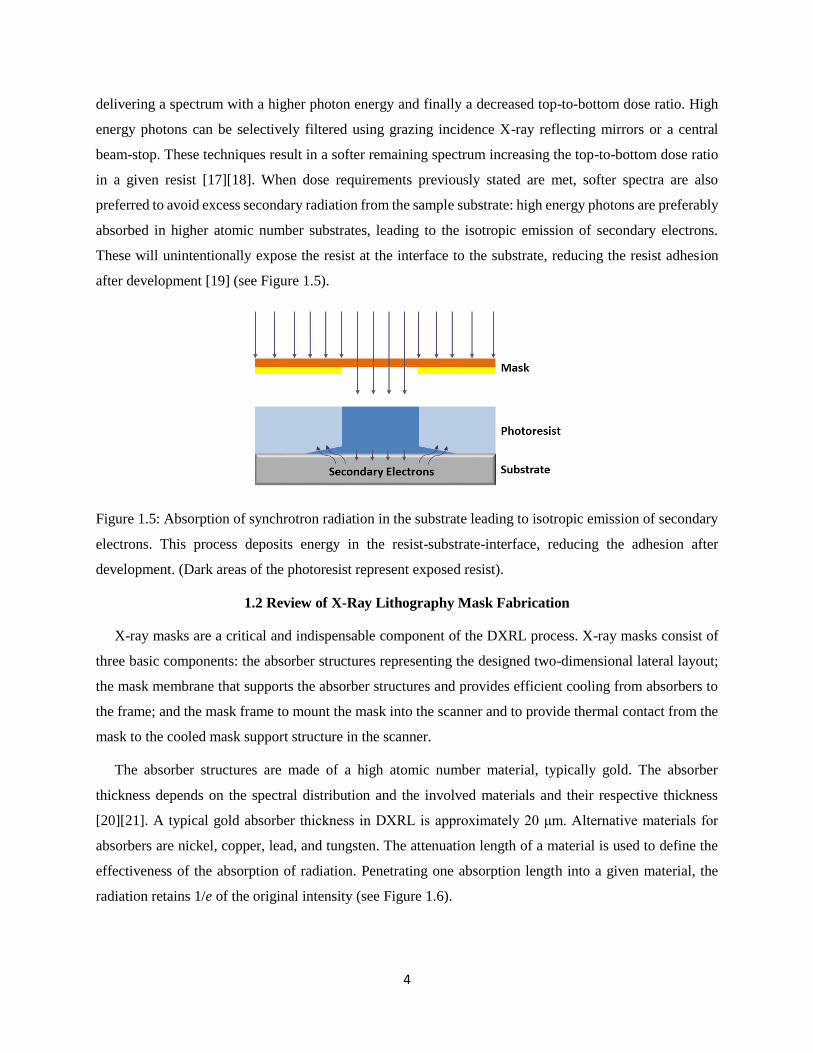
Figure 1.5: Absorption of synchrotron radiation in the substrate leading to isotropic emission of secondary
electrons ........................................................................................................................................................ 4
Figure 1.6: X-ray attenuation length [μm] of different mask absorber materials for photon energies from 1
to 15 keV. ...................................................................................................................................................... 5
Figure 1.7: Spectral transmission of different mask membrane materials at the thicknesses from Table 1.1.
...................................................................................................................................................................... 6
Figure 1.8: Fluorescence radiation from the X-ray mask membrane. ........................................................... 8
Figure 1.9: Thermal expansion during X-ray exposure ................................................................................ 9
Figure 1.10: Typical fabrication sequences for X-ray masks ..................................................................... 10
Figure 1.11: Schematic of the SyLMAND beamline .................................................................................. 12
Figure 1.12: Schematic of the intensity chopper disk ................................................................................. 13
Figure 1.13: SyLMAND spectral power ..................................................................................................... 14
Figure 1.14: SyLMAND beam power impinging onto the sample ............................................................. 14
Figure 1.15: SyLMAND scanner stage with assembly of mask and mask holder as well as the substrate
holder in the opened position. ..................................................................................................................... 15
Figure 1.16: Cooling plate of the SyLMAND mask holder ........................................................................ 16
Figure 2.1: Artistic view of molecule chain disorientation due to increased film thickness. ..................... 19
Figure 2.2: Fabrication process for the polyimide X-ray mask by Optnics Precision ................................ 20
Figure 2.3: Micrographs of a test structure with 10 μm nominal line width.. ............................................. 21
Figure 2.4: Optical micrograph of a typical P84® polyimide membrane surface after mixing, spin-coating
and curing.................................................................................................................................................... 24

xi
Figure 2.5: Layout of the center block test mask ........................................................................................ 25
Figure 2.6: Optical micrograph of a Durimide 7520® polyimide membrane. ............................................. 27
Figure 2.7: Scanning Electron Micrographs of the sputtered titanium layer on polyimide ........................ 28
Figure 2.8: Setup of nickel electroplating ................................................................................................... 30
Figure 2.9: Image of a processed mask. ...................................................................................................... 31
Figure 2.10: Complete coverage test mask seen from the front side .......................................................... 31
Figure 2.11: Center block test mask seen from the front side. .................................................................... 32
Figure 2.12: Fabrication sequence developed for polyimide X-ray masks at SyLMAND. ........................ 33
Figure 3.1: Schematic of the simplified model for thermal simulations ..................................................... 36
Figure 3.2: X-ray transmission of the X-ray mask components from 1 to 15 keV ..................................... 38
Figure 3.3: Schematic of the simplified mask model for thermoelastic simulations .................................. 38
Figure 3.4: Schematic of the DXRL exposure model used in the simulation of the complete coverage
mask. ........................................................................................................................................................... 39
Figure 3.5: Thermal balance of the model .................................................................................................. 40
Figure 3.6: Components of stress in three dimensions. .............................................................................. 41
Figure 3.7: Left: FEM mesh of the complete coverage mask for the thermoelastic simulation; Right:
details of the elements used in the mesh. .................................................................................................... 44
Figure 3.8: Simulated temperatures with respect to flow time at the locations where the five
thermocouples are placed in the experiments for the complete coverage mask. ........................................ 46
Figure 3.9: Simulated temperature distribution when the beam is at the location of the top thermocouple
(#2) and the temperature reaches its highest values in that location. Simulation for the complete coverage
mask. ........................................................................................................................................................... 47
Figure 3.10: Simulated temperature distribution when the beam is at the location of the center
thermocouple (#5) and the temperature reaches its highest values in that location. Simulation for the
complete coverage mask. ............................................................................................................................ 47
Figure 3.11: Simulated temperatures with respect to flow time at the locations where the five
thermocouples are placed in the experiments for the center block mask .................................................... 48
xii
Figure 3.12: Simulated temperature distribution when the beam is at the location of the top thermocouple
(#2) and the temperature reaches its highest values in that location. Simulation for the center block mask.
.................................................................................................................................................................... 49
Figure 3.13: Simulated temperature distribution when the beam is at the location of the center
thermocouple (#5) and the temperature reaches its highest values in that location. Simulation for the
center block mask. ...................................................................................................................................... 49
Figure 3.14: Simulated total (3-dimensional) deformations (in micrometers) for the complete coverage
mask ............................................................................................................................................................ 50
Figure 3.15: Simulated deformations (in micrometers) in the lateral plane along the x-axis (orthogonal to
the incident synchrotron beam) for the complete coverage mask ............................................................... 51
Figure 3.16: Simulated deformations (in micrometers) in the lateral plane along the y-axis (orthogonal to
the incident synchrotron beam) for the complete coverage mask ............................................................... 51
Figure 3.17: Simulated deformations (in micrometers) along the z-axis (along the beam direction,
orthogonal to the lateral plane) for the complete coverage mask ............................................................... 52
Figure 3.18: Simulated equivalent stress distributions (in MPa) for the complete coverage mask ............ 52
Figure 3.19: Simulated total (3-dimensional) deformations distributions (in micrometers) for the center
block mask .................................................................................................................................................. 53
Figure 3.20: Simulated deformations (in micrometers) along the x-axis (orthogonal to the incident
synchrotron beam) for the center block mask ............................................................................................. 53
Figure 3.21: Simulated deformations (in micrometers) along the y-axis (orthogonal to the incident
synchrotron beam) for the center block mask ............................................................................................. 54
Figure 3.22: Simulated deformations (in micrometers) along the z-axis (along the beam direction,
orthogonal to the lateral plane) for the center block mask .......................................................................... 54
Figure 3.23: Simulated equivalent stress distributions (in MPa) for the center block mask ....................... 55
Figure 3.24: 3D schematic of the center block absorber deformation when the beam is at the location of
the center thermocouple (#5) (deformation scaled by 200). ....................................................................... 58
Figure 3.25: Simulated temperature distribution after 19.0 seconds when the beam is at the location of the
center thermocouple (#5) and the temperature reaches its highest values in that location. Simulation for
the complete coverage mask, exposure without intensity chopper implementation. .................................. 59

xiii
Figure 3.26: Simulated deformations (in micrometers) for the complete coverage mask, exposure without
intensity chopper implementation ............................................................................................................... 60
Figure 4.1: Vertical beam profile scanned with the fly-wire photocurrent measurement system at the
mirror entrance ............................................................................................................................................ 62
Figure 4.2: Schematics of the positioning of the five thermocouples on the test masks............................. 64
Figure 4.3: Experimental setup of the complete coverage mask, mask holder, scanner adapter, and five
thermocouples. ............................................................................................................................................ 64
Figure 4.4: Experimental setup of the center block mask, mask holder, scanner adapter, and 5
thermocouples. ............................................................................................................................................ 65
Figure 4.5: Maximum temperatures at the center thermocouple (#5) measured for various computed
incident beam powers with the complete coverage mask ........................................................................... 68
Figure 4.6: Maximum temperatures at the center thermocouple (#5) measured for various computed
incident beam powers with the center block mask...................................................................................... 69
Figure 4.7: Simulated (solid line) and measured (dotted line) temperature with respect to time at the
location of the center thermocouple (#5) for the complete coverage mask. ............................................... 70
Figure 4.8: Simulated (solid line) and measured (dotted line) temperature with respect to time at the
location of the center thermocouple (#5) for the center block mask. .......................................................... 70
Figure 4.9: Schematic of the tilted substrate holder during the measurements. .......................................... 71
Figure 5.1: Extended DXRL exposure simulation model with PMMA-wafer assembly: cross-sectional
view of the synchrotron beam impinging onto the modeled layers. ........................................................... 73
Figure 5.2: Simulated temperatures with respect to flow time at the location of the center thermocouple
(#5) for the complete coverage mask using the intensity chopper with 25% open duty cycle ................... 74
Figure 5.3: Simulated mask temperature distribution when the beam is at the location of the center
thermocouple (#5) and the temperature reaches its highest values in that location. Simulation for the
nickel absorber in the complete coverage mask. ......................................................................................... 75
Figure 5.4: Simulated resist temperature distribution when the beam is at the location of the center
thermocouple (#5) and the temperature reaches its highest values in that location. Simulation for the
PMMA resist on the silicon wafer behind the complete coverage mask. ................................................... 75
Figure 5.5: Beam power density distribution in the various layers of the extended DXRL exposure model
for the center block mask ............................................................................................................................ 76

xiv
Figure 5.6: Simulated temperature distribution when the beam is at the location of the center
thermocouple (#5) and the temperature reaches its highest value in that location. Simulation for the center
block mask in front of 250 μm PMMA. ...................................................................................................... 78
Figure 5.7: Simulated resist temperature distribution when the beam is at the location of the center
thermocouple (#5) and the temperature reaches its highest value in that location. Simulation for 250 μm
PMMA resist on the silicon wafer behind the center block mask. .............................................................. 78
Figure 5.8: Simulated temperature distribution when the beam is at the location of the center
thermocouple (#5) and the temperature reaches its highest value in that location. Simulation for the center
block mask in front of 500 μm PMMA. ...................................................................................................... 79
Figure 5.9: Simulated resist temperature distribution when the beam is at the location of the center
thermocouple (#5) and the temperature reaches its highest value in that location. Simulation for 500 μm
PMMA resist on the silicon wafer behind the center block mask. .............................................................. 79
Figure 5.10: Schematic of the PMMA-wafer assembly model ................................................................... 80
Figure 5.11: Simulated deformations (in micrometers) for the center block mask in front of 250 μm
PMMA ........................................................................................................................................................ 81
Figure 5.12: Simulated deformations (in micrometers) for the 250 μm thick PMMA layer behind the
center block mask ....................................................................................................................................... 82
Figure 5.13: Simulated deformations (in micrometers) for the center block mask in front of 500 μm
PMMA. ....................................................................................................................................................... 83
Figure 5.14: Simulated deformations (in micrometers) for the 500 μm thick PMMA layer behind the
center block mask ....................................................................................................................................... 84
Figure A.1: Relationship between spin speed and cured film thickness for Durimide 7520®. ................... 92
Figure B.1: Positions of surface roughness measurements for the titanium layer. ..................................... 93

xv
LIST OF ABBREVIATIONS
CLS Canadian Light Source
DMSO Dimethyl Sulfoxide
DXRL Deep X-Ray Lithography
LIGA German acronym for lithografie, galvanoformung, and abformung
MEMS Microelectromechanical Systems
NEP N-ethyl-pyrrolidone
PMMA Polymethyl Methacrylate
PVD Physical Vapor Deposition
SEM Scanning Electron Microscope
SR Synchrotron Radiation
SyLMAND Synchrotron Laboratory for Micro and Nano Devices
TMAH Tetramethyl Ammonium Hydroxide
XRL X-Ray Lithography

1
CHAPTER 1
INTRODUCTION
1.1 Overview of X-Ray Lithography Technology
X-ray lithography (XRL) has been developed since the 1970s with further developments still being made
today. It utilizes high energy photons within the spectrum of X-rays to transfer absorber patterns on an X-
ray mask into a photosensitive layer coated onto a substrate [1][2]. In the 1980s, deep X-ray lithography
(DXRL) using hard X-rays of 2 to 15 keV became a vital step in the LIGA process. LIGA is a German
acronym for lithography, electroplating, and replication. The technology was developed by
Forschungszentrum Karlsruhe, Germany (FZK/IMT) [3][4]. Combined with subsequent electroplating and
molding steps, mass production of microstructures becomes possible (see Figure 1.1).
Figure 1.1: The LIGA process: (a) Lithography: X-ray lithography using synchrotron radiation to expose a
thick resist layer through an X-ray mask; (b) Electroplating: Electrodeposition of metal in the resist
template fabricated in step (a); (c) Replication: Molding of a polymer using the metallic molding tool
fabricated in step (b). [5]
LIGA technology enables fabrication of high aspect ratio micro structures (the ratio between height and
width of the structures, up to some hundreds) with high lateral accuracy, and optically smooth, vertical
sidewalls [6][7]. The exposure process typically involves synchrotron radiation (SR) [8]. Synchrotron
radiation is produced when electrons orbit almost at the speed of light, e.g. in an electron storage ring. The
centripetal acceleration of the charged particles in bend magnets leads to the emission of electromagnetic
radiation. Due to relativistic effects, the radiation is highly collimated as it proceeds down the X-ray
beamline. On its way to the sample, the beam passes the X-ray mask. Where the X-rays impinge onto mask
absorbers made of high atomic number Z elements, such as gold, they get completely absorbed. In mask
areas without absorber patterning, the X-rays pass the mask membrane and a small proximity gap to
impinge onto the photoresist on a substrate, causing local photo-chemical reactions. Thus, an image of the
lateral mask absorber pattern is formed by shadow projection. The chemical properties of the exposed
photoresist get locally modified, which turns the exposed photoresist to be selectively soluble or insoluble,

2
depending on the resist type, in a subsequent wet-chemical development step. The synchrotron beam
usually covers the entire width of the sample to be exposed. In the vertical direction, the collimation limits
the exposure height to a few millimeters. Homogeneous exposure of several centimeter large samples can
only be achieved if the stack of mask and sample is vertically oscillated through the synchrotron beam. This
task is accomplished in an X-ray scanner, which precisely controls the motion, ensuring constant
mechanical mounting and constant velocities during each stroke (see Figure 1.2).
Figure 1.2: Artistic view of DXRL exposure: Left: Bend magnet accelerating the electron trajectory, leading
to tangential emission of photons (synchrotron radiation); Right: Side view inside the vacuum chamber of
an X-ray scanner for DXRL. The X-ray mask (consisting of mask frame, mask membrane, and mask
absorber structures) and the sample (consisting of photoresist and silicon wafer) is vertically oscillated
(scanned) through the incident synchrotron beam (Dark areas of the photoresist represent exposed resist).
Photoresists can be divided into two types: positive tone and negative tone resists. For positive tone
resists, exposed regions will get soluble in the developer. For negative tone resists, exposed regions become
insoluble in the developer (see Figure 1.3). The most commonly used positive tone resist in DXRL is
Polymethyl Methacrylate (PMMA, [C5H8O2]n) [9]. A typical negative tone resist is SU-8 which was
developed by IBM in the 1990s [10].
Figure 1.3: Lithographic patterning of positive and negative tone resists (Dark areas of the photoresist
represent exposed resist).

3
A vital parameter in lithographic exposure is the power density of the radiation absorbed in the resist,
referred to as the exposure dose. In DXRL, the exposure dose is a volumetric quantity. It is impacted by the
radiation spectrum as well as the absorber and resist material properties and layer thicknesses. Three target
dose values are typically defined: the dose deposited at the top of the exposed photoresist (Dtop); the dose
deposited at the bottom of the exposed photoresist (Dbottom); and the dose unintentionally deposited at the
top of the nominally unexposed photoresist (Dunexposed) due to finite mask absorber contrast and secondary
effects [11][12] (see Figure 1.4). For positive-tone resist, the dose deposited at the top of the exposed resist,
Dtop, may not exceed an upper limit since the photoresist would massively foam if too much energy was
absorbed. This could damage the adjacent unexposed resist areas or even the mask. The dose deposited at
the bottom of the exposed resist, Dbottom, has a minimum threshold to ensure residual-free development at a
chosen overall development time [13]. These restrictions result in a top-to-bottom dose ratio for the exposed
resist with an optimum value for different resist types and layer thickness. To meet these dose requirements,
the spectral distribution of the synchrotron beam and the exposure time must be adjusted for each individual
exposure.
Figure 1.4: Local exposure dose values relevant for determining the optimum exposure conditions. (Dark
areas of the photoresist represent exposed resist).[14]
For the positive tone photoresist PMMA, the maximum allowed dose is 20 kJ/cm3, while typically a
safer dose value of 12 kJ/cm3 is chosen for the top of the exposed resist. The minimum exposure dose
deposited at the bottom of the exposed PMMA is usually assumed to be about 3 kJ/cm3. The dose deposited
in the unexposed PMMA under the absorber structures must remain less than 0.1 kJ/cm3 [15]. For the
negative photoresist SU-8, the required dose deposition is only 50-100 J/cm3 [16].
As previously mentioned, these dose requirements are met by spectral adjustment. Both, low and high
energy photons may need to be filtered from the incident beam spectrum. The soft spectral contributions
can be reduced by low-atomic number pre-absorbers, such as beamline vacuum windows or X-ray filters
to be introduced into the beamline. In both cases, low energy contributions of the spectrum are filtered most,
4
delivering a spectrum with a higher photon energy and finally a decreased top-to-bottom dose ratio. High
energy photons can be selectively filtered using grazing incidence X-ray reflecting mirrors or a central
beam-stop. These techniques result in a softer remaining spectrum increasing the top-to-bottom dose ratio
in a given resist [17][18]. When dose requirements previously stated are met, softer spectra are also
preferred to avoid excess secondary radiation from the sample substrate: high energy photons are preferably
absorbed in higher atomic number substrates, leading to the isotropic emission of secondary electrons.
These will unintentionally expose the resist at the interface to the substrate, reducing the resist adhesion
after development [19] (see Figure 1.5).
Figure 1.5: Absorption of synchrotron radiation in the substrate leading to isotropic emission of secondary
electrons. This process deposits energy in the resist-substrate-interface, reducing the adhesion after
development. (Dark areas of the photoresist represent exposed resist).
1.2 Review of X-Ray Lithography Mask Fabrication
X-ray masks are a critical and indispensable component of the DXRL process. X-ray masks consist of
three basic components: the absorber structures representing the designed two-dimensional lateral layout;
the mask membrane that supports the absorber structures and provides efficient cooling from absorbers to
the frame; and the mask frame to mount the mask into the scanner and to provide thermal contact from the
mask to the cooled mask support structure in the scanner.
The absorber structures are made of a high atomic number material, typically gold. The absorber
thickness depends on the spectral distribution and the involved materials and their respective thickness
[20][21]. A typical gold absorber thickness in DXRL is approximately 20 μm. Alternative materials for
absorbers are nickel, copper, lead, and tungsten. The attenuation length of a material is used to define the
effectiveness of the absorption of radiation. Penetrating one absorption length into a given material, the
radiation retains 1/e of the original intensity (see Figure 1.6).

5
Figure 1.6: X-ray attenuation length [μm] of different mask absorber materials for photon energies from 1
to 15 keV. [22]
The mask membrane supports the absorber structures, defining their exact position. It also dissipates
heat in the absorbers to the supporting frame. The membrane should meet the following criteria: 1) lowest
possible X-ray absorption to allow for good transmission (ratio of transmitted to incident power) of X-rays
to the resist to be exposed and a good contrast when compared to the transmission through absorbers; 2)
highest possible mechanical strength to safely support the mask absorbers even under thermal stress and to
allow for larger mask formats; 3) sufficient electrical conductivity to allow for electroplating of the metal
absorbers during the mask fabrication process; 4) good adhesion of the mask absorbers to avoid
delamination during use; 5) constant thickness to avoid uneven absorption in the membrane (e.g., absence
of pinholes, little or no wedge-error in membrane thickness, limited roughness); 6) good availability and
economic affordability; 7) non-toxic materials to allow for a broad fabrication process selection; 8)
sufficient stability when exposed to X-rays; and 9) optical transparency to allow for aligned exposure.
A variety of materials have been explored and used for mask membrane applications, such as silicon
nitride, silicon carbide, silicon, beryllium, graphite, glass, titanium, and polyimide. Some selected
characteristics of the most frequently used materials are compiled in Table 1.1. It shows that none of the
materials is a perfect mask membrane material. While beryllium, for instance, has outstanding thermal
properties and is sufficiently X-ray transparent to allow for mechanically stable membrane thicknesses, it
is toxic, hard to machine to the required specifications, optically not transparent, and both expensive as well
as with limited availability from only one vendor world-wide. Polyimide, on the other hand, is optically
transparent, cheap, non-toxic, and reasonably stable as far as mechanical properties are concerned, but only

6
features limited stability against X-rays, and has very poor thermal properties. The spectral transparencies
of the mask membrane materials mentioned in Table 1.1 are presented in Figure 1.7. The transmission is
defined as the ratio of the transmitted power to the incident power. The values are calculated based on the
membrane thickness from Table 1.1.
Figure 1.7: Spectral transmission of different mask membrane materials at the thicknesses from Table 1.1.
[22]

Table 1.1: The characteristics of X-ray mask membrane materials [14][23]
Material Density
(g/cm3)
Young’s
Modulus
(GPa)
Type of
Membrane
Typical
Substrate
Thickness
(μm)
Thermal
Conductivity
(W/m/K)
Thermal
Expansion
Coefficient
(10-6/K)
Typical
Fabrication
Technique
Cost
Surface
Roughness
(nm)
Beryllium 1.85 300 Self-supported >250 200 12.3 Machining High 500
Graphite 1.7-1.8 N/A Self-supported >100 95 8.1 Machining Low <1000
Silicon
Nitride 2.4 160-390 Suspended 1 16-33 0.8-2.7 CVD High N/A
Titanium 4.5 120 Suspended 2.8 20-30 9 PVD High N/A
Polyimide 1.2 >3 Suspended 50 0.12 55 Spin coating Low N/A
7

8
Selected mask membrane materials have further disadvantages beyond those apparent in Table 1.1,
causing secondary effects [19]. First, some mask membrane materials will, during exposure to high energy
photons as found in synchrotron radiation, emit secondary fluorescence radiation. This fluorescence
radiation has energies characteristic of the membrane material and is emitted isotropically (i.e. without
preferred direction), leading to an extra dose deposition at the top corners of the nominally unexposed resist
areas. After development, bevelled edges can be observed (see Figure 1.8). For example, titanium has the
K-shell absorption edge at 4.97 keV, which is within the synchrotron spectrum used for DXRL exposure
[24]. Such secondary fluorescence can penetrate the resist up to several hundred micrometers deep. To
reduce the impact of the fluorescence radiation, low atomic number X-ray filters such as polyimide foils
can be inserted between the mask and substrate during exposure. A more fundamental approach is changing
the membrane material: lower atomic number materials, such as beryllium, do not exhibit noticeable
fluorescence.
Figure 1.8: Fluorescence radiation from the X-ray mask membrane. (Dark areas of the photoresist represent
exposed resist).
A major concern for selecting mask membrane materials is the thermal conductivity: the beam power
absorbed in the X-ray mask is primarily dissipated as heat, which can lead to increased temperatures in
mask and sample, resulting in non-uniform thermal expansion and ultimately in thermal deformations of
the mask and sample (see Figure 1.9) [19]. To control the temperature rise in the X-ray mask, it is critical
to provide sufficient cooling through the mask frame to the cooled scanner adapter, and to allow good heat
transfer from the mask absorbers to the mask frame by using thermally well conducting membranes. Where
this is not possible, the incident beam power must be reduced to limit the temperature rise. This power
reduction can be achieved by decreasing the electron current in the storage ring; by using an intensity
chopper; or by insertion of pre-absorber in front of the mask [19]. These thermal effects will be further
discussed in Section 1.5.

9
Figure 1.9: Thermal expansion during X-ray exposure: deformations of the mask absorbers from the ideal
dimensions (broken red lines) and ultimately to reduced accuracy of the exposed resist area (dark area).
During fabrication, the mask absorbers are generated by filling the voids in a polymer template, using
an electroplating process. This process requires an electrically conductive layer. If the mask membrane is
not conductive, an intermediate thin film plating base is required. A typical plating base material in DXRL
is gold, while another is TiOx. The latter has X-ray optical advantages over gold, but requires to avoid the
formation of the natural oxide TiO2 which is a dielectric. A complex compound must be formed by partial
oxidization of the titanium layer [25]. This ensures high electrical conductivity and a passivated surface to
protect from further oxidization. Furthermore, the slightly rough surface structure of the TiOx promotes the
adhesion between mask membrane and absorber structures by mechanical interlocking.
The mask frame of an X-ray mask supports the mask membrane, facilitates mounting of the mask in the
scanner, and provides efficient cooling of the entire mask when a good contact is established to the cooled
scanner. Mask frames are available in a variety of formats. One of them is laid out for a round mask of 4-
inch diameter. A manufacturing standard for this format was developed by APRA-NIST in the 1990s
[26][27]. It offers a 4” outer diameter (101.6 mm) and an exposable net diameter of 83 mm as the exposure
window. The material of this mask frame is an aluminum alloy or stainless steel.
Besides the materials for the three main components, and the involved dimensions, micro patterning of
the mask absorbers is also important. The sidewalls of the absorbers must be vertical and straight to provide
a sharp contrast between transparent and opaque mask areas [28]. Typical absorber thicknesses of
approximately 20 μm gold are sufficient in many cases. Since XRL is based on shadow projection, the
lateral absorber dimensions are identical with the exposed sample. Mask absorbers must therefore have
vertical walls, relatively large thickness, and small lateral resolution. No standard fabrication technique
satisfies all these requirements simultaneously. Highest resolution patterning using electron beam writers,
for instance, allows to fabricate a few micrometer deep resist templates, but not 20 μm thick [29]. Optical
patterning using UV lithography, on the other hand, can provide sufficiently deep structures, but only at

10
significantly reduced lateral resolution. X-ray masks are therefore typically fabricated in a more or less
complex sequence of various patterning and copying steps, often involving thinner intermediate and full-
height X-ray masks. Typical fabrication sequences for X-ray masks are presented in Figure 1.10. X-ray
masks obtained from different sequences vary with respect to achievable minimum resolution, which is as
also referred to as the critical dimension (CD). Figure 1.10 also presents some rough estimates for the CD
associated with different sequences. The cost of fabrication varies with equipment and material expenses,
and also increases with the number of steps.
Figure 1.10: Typical fabrication sequences for X-ray masks [14]
The research presented in this thesis focuses on the thermal and thermoelastic behavior of X-ray masks
rather than the patterning accuracy of the absorbers. The most cost-effective and fastest patterning approach
has therefore been chosen, referred to as the ‘low resolution’ sequence: the layout of a UV mask is copied
into the resist of the X-ray mask. Ultimately, this research is meant to contribute to the development of an
integrated, new, high resolution patterning sequence in which a laser writer will be applied to pattern a thin
intermediate mask based on an economic mask membrane.
1.3 Review of Thermal and Mechanical Analyses of X-ray Exposure
DXRL involves synchrotron radiation, and physical and chemical processes during exposure and
development are affected by a huge variety of dependant parameters. Complicated equations describe the

11
exact properties of synchrotron radiation, and these can be extended to model components of the exposure
and development process and the resulting structure accuracies. Thermal and mechanical properties
constitute key technical issues, and their analysis has been an ongoing part of DXRL research. Various
mathematical models and numerical analyses of the lithographic exposure process have been reported
[30][31][32][33]. These studies include several exposure parameters and conditions that determine the
temperature rise in the model, such as the spectral and beam power parameters, the beam geometry, the
sample geometry, including the proximity gap distance between mask and sample as well as the scanning
parameters, and the involved materials properties like the mask absorbers, the membrane, the surrounding
gas, and the resist and substrate. The possible heat transfer mechanisms include conduction, convection,
and radiation. Thermal conduction from absorbers through the mask membrane, across the proximity gap
and photoresist, to the cooled substrate has been identified to dominate the heat dissipation from the X-ray
mask to the scanner.
Various approaches have been applied to measure the temperature of the X-ray mask during exposure
in real time. One way is to monitor the temperature distribution in the mask during exposure using an
infrared camera, as a resolution of 0.1°C can be achieved [34][35]. Another way is to fabricate metal
structures on the X-ray mask as a built-in thermistor (thermal resistor), converting a temperature change
into a resistance change, with a sensitivity of up to 0.02°C [36]. Last but not least, thermocouples are applied
by researchers to measure the temperature of the X-ray mask [37]. A drawback of adding any metal sensor
is that they can only be reliably applied behind mask absorbers. They cannot deliver accurate data for the
temperature distribution in the open mask membrane, as the metal sensors themselves would strongly
absorb radiation, and consequently further heat up the system.
Many studies analyzed thermoelastic deformations of the X-ray mask during exposure [38][39][40].
Thermal expansion of the mask frame can usually be neglected since it is normally made of a thermally
well conducting metal, and is in close or direct contact to scanner parts which are often water-cooled,
keeping the mask frame at ambient temperatures. The deformations in the mask membrane can be divided
into out-of-plane deformations (along the incident beam) and in-plane deformations (within the mask plane)
[41]. [42][43] also studied the buildup of the internal stress in the mask membrane and the absorber
structures caused by the initial mask fabrication were experimentally verified.
1.4 Experimental Setup in the Synchrotron Laboratory for Micro and Nano Devices (SyLMAND)
The Canadian Light Source (CLS) in Saskatoon, Saskatchewan, is a 3rd generation synchrotron light
source with an electron energy of 2.9 GeV and a stored current of up to 250 mA. The bend radius is 7.1428
m, delivering a critical energy of the radiation spectrum of 7.6 keV [44]. This energy divides the broad-
band, continuous spectrum, which ranges from infrared to hard X-rays, into two halves of equal beam power.

12
The Synchrotron Laboratory for Micro and Nano Devices (SyLMAND) at the CLS is Canada’s only
dedicated DXRL facility, applying an adjustable synchrotron spectrum between approximately 1 keV and
15 keV. The total length of the beamline from the bending magnet to the X-ray scanner is 16.91 m (see
Figure 1.11). The beamline can be divided into the front end section, the optics section, and the experimental
section or ‘end station’. Most of the beamline sections are kept in an ultra-high vacuum, with typical
pressure below 5·10-9 mbar. The major beamline components are an intensity chopper for beam power
adjustment, a double mirror system for spectral beam adjustment, and an X-ray scanner (DEX04,
manufactured by Jenoptik GmbH; Jena, Germany) for homogeneous sample exposure under an inter gas
atmosphere.
Figure 1.11: Schematic of the SyLMAND beamline. [45]
The synchrotron radiation is generated in the bend magnet in the storage ring, guided through the front
end and through the radiation protection wall (grey block in Figure 1.11), and then enters the optics section.
The intensity chopper the first major component of the optics section. It adjusts the beam power by
varying the duty cycle of completely transparent (‘beam on’) and completely opaque (‘beam off’) time
periods. The intensity chopper is a rotating invar steel disk with 31 periodically arranged openings. In a
final stage, these openings can continuously be adjusted. In the current implementation, each opening has
two defined widths (see Figure 1.12). The duty cycle is determined by the width of these slots, resulting in

13
either 10% or 25% time-averaged transparency. The intensity chopper is mounted orthogonally to the
synchrotron beam, intercepting the beam by rotating at a constant speed of 400 rpm. The rotation speed is
fast enough to avoid resonance phenomena between the scanned sample and rotating intensity chopper. The
intensity chopper can also be moved out of the beam to deliver the full beam power to the subsequent
components [45].
Figure 1.12: Schematic of the intensity chopper disk. (connection beam to the center rotation shaft not
included) [45]
The x/y slits can collimate the beam width and height. The four fly-wire systems allow the beam
intensity to be measured in both vertical and horizontal direction, both at the entrance and exit of the double
mirror system. The double mirror system can be applied to adjust the spectrum of the synchrotron beam by
absorption of high energy photons. Both grazing incidence mirrors are cooled and coated with chromium.
The mirror angles can be changed individually to tune the spectral adjustment: photons with energies
exceeding the angle-dependent cut-off energy are absorbed, while the rest are reflected down the beamline
(see Figure 1.13 and Figure 1.14) [49].

14
Figure 1.13: SyLMAND spectral power: after 110 μm beryllium vacuum windows; without and with double
mirror system at various grazing incidence angles between 4 and 25 mrad. [45]
Figure 1.14: SyLMAND beam power (at 250 mA) impinging onto the sample: after the front end; after
front end and 110 μm beryllium vacuum windows (261 W); and after frontend, vacuum windows and
double mirror system as a function of various grazing incidence angles between 4 and 45 mrad. [45]

15
Finally, the synchrotron beam passes the filter chamber for additional spectral adjustment and the second
vacuum window to the scanner end station where it impinges onto the mask and sample. Two pairs of
apertures in vertical and horizontal directions will define the beam size in width and height, which can be
adjusted for special exposure requirements.
During exposures, the scanner chamber is filled with 100 mbar helium gas as a buffering environment.
Helium provides better heat dissipation than ultra high vacuum would, and at the same time limits the
unwanted X-ray absorption at higher gas pressure or ambient air [47]. It also prevents the scanner form
corrosion, avoiding the transformation of oxygen into reactive ozone under the impact of X-rays [48].
Figure 1.15 shows a photograph of the SyLMAND scanner stage in the opened position. The assembly
of mask and mask holder is seen in its vertical position, while the substrate holder is currently flapped down
to a horizontal position for mask and sample loading. When lifted and pushed against the mask, the
proximity gap between sample and mask is controlled by proximity shims of typically 50 or 100 μm
thickness [49]. During the exposure process, the complete stage assembly is vertically oscilated by an
electric motor, scanning the stack of mask and sample through the synchrotron beam.
Figure 1.15: SyLMAND scanner stage with assembly of mask and mask holder as well as the substrate
holder in the opened position.

16
The mask holder and substrate holder are both water-cooled. A copper plate with a cooling water tube
is brazed to the upstream side of the mask holder to dissipate heat (see Figure 1.16). The substrate holder
is internally cooled.
Figure 1.16: Cooling plate of the SyLMAND mask holder (view from the upstream side of the scanner).
1.5 Motivation and Research Objectives
DXRL can be applied to produce polymer or metal microstructures with high aspect ratios and
outstanding structure quality. However, it is a particularly expensive MEMS (Microelectromechanical
Systems) fabrication technology [50]. Besides cost of exposure, cost associated with mask fabrication is
the main reason. Availability and timelines to delivery are also quite limited. Finally, all of the mask
fabrication concepts available to date suffer from drawbacks associated with the materials selection or
patterning technology. At SyLMAND, a novel masking approach is currently getting developed, merging
high resolution patterning by a laser writer as a rapid fabrication approach with other cost and time saving
options. A key role plays establishing a polymer mask membrane that is robust, affordable, available, as
well as process compatible. Polyimide might be a promising membrane material for good X-ray
transmission, absence of fluorescence effects that could reduce the structure accuracy, and outstanding
thermal and chemical stability. Thermal deformations during synchrotron exposure, however, have

17
previously ruled out successful implementation. The continuous tuning capabilities at SyLMAND allow to
revisit thermal issues and adjust the process parameters for optimized conditions.
The purpose of this thesis is to investigate whether polyimide could successfully be applied as an X-ray
mask membrane material at SyLMAND, what the thermal boundary conditions would be, and how a
fabrication process could get implemented.
Specific objectives of this research are to:
1. Identify the properties of polyimide as a potential mask membrane material in DXRL, and determine
which kind of polyimide material should be further pursued.
2. Develop a numerical model for a polymer-based mask with different absorber structures to study the
impact of different exposure conditions accessible at SyLMAND, and the thermal/thermoelastic
behaviour of the test masks during exposure.
3. Develop a fabrication sequence for polymer mask membranes and their integration with a plating base
and a suitable mask frame.
4. Integrate such a mask with basic absorber structures to fabricate a complete test mask used to
experimentally determine the thermal conditions during exposure and to verify the numerical model.
5. Apply the numerical and experimental results to model thermal deformations under exposure conditions
to be expected at SyLMAND for practical applications, and determine intensity chopper settings to limit
the deformations to an acceptable level.
1.6 Thesis Organization
This thesis is organized into six chapters.
In Chapter 2, the polymer mask membrane material is further pursued, and fabrication techniques for
the polyimide X-ray test mask are developed. This includes patterning of basic absorber structures,
delivering a detailed fabrication process for two test masks: one is completely covered with nickel absorber,
while the other one has an isolated center block absorber layout.
In Chapter 3, numerical analyses of the thermal and thermoelastic behavior of the test masks are carried
out. A numerical model is developed by computational fluid dynamics to simulate the temperature
distributions in the two test masks during X-ray exposure. The resulting thermal deformations in the test
masks are evaluated at selected time steps during the exposure by finite element analysis.
Chapter 4 provides experimental verification of the thermal simulation. The temperature distributions
in the two test masks are measured by thermocouples during synchrotron beam exposure. Different beam

18
parameters are applied in the experiments in order to obtain a variety of beam powers. In addition, the
relationship between temperature in the test masks and incident beam powers is discussed.
Chapter 5 merges the results of the preceding numerical analysis, presenting a prediction of the thermal
and thermoelastic behaviors of the test masks and PMMA resist in typical DXRL exposure scenarios, which
are based on different resist thicknesses.
Chapter 6 consists of the summary and conclusion of the research, along with suggestions for future
work.

19
CHAPTER 2
POLYIMIDE MATERIALS SELECTION AND FABRICATION PROCESS DEVELOPMENT OF
TEST MASKS
2.1. Review of Material Properties of Polyimide as a Potential Mask Membrane Material
Polyimide is a polymer which has been widely applied in various industrial fields since it was first
synthesized in 1908 [51]. It has excellent thermal stability and good mechanical and chemical properties to
serve as membranes in various technological contexts [52]. Various grades of polyimide have been
industrially developed, e.g. Kapton® manufactured by DuPont. Among different types of polyimides, photo-
definable ones, such as the HD series by HD microsystems and the Durimide® series by Fujifilm, have been
applied in the semiconductor industry because of their excellent thermal and chemical stabilities and their
low dielectric constants [53][54].
2.1.1 Thermal and Mechanical Properties
Polyimide has a thermal conductivity of about 0.12 W/m/K. This is a very low value when compared to
other membrane materials, including many polymers. A closer look reveals that the exact thermal
conductivity of polyimide varies with the thickness and the orientation of the material. An anisotropy of
the thermal conductivity has been reported for polyimide thin films of 0.5 to 2.5 μm thickness [55]. A
significant disparity between lateral and vertical thermal conductivity was observed, which decreases as the
film thickness increases. The degree of cross-linking increases as the material becomes less reduced in the
vertical dimension, and the long chain molecules will be more disoriented with less molecule planarity as
they are highly cross-linked (see Figure 2.1). [56]
Figure 2.1: Artistic view of molecule chain disorientation due to increased film thickness, leading to
reduced anisotropy.
Many factors have influence on the mechanical properties of polyimides: molecular structure, molecular
weight (Mw), preparation procedure, and heating history [57]. In general, polyimides exhibit modulus values
of 1.5 to 3.0 GPa. Mechanical properties of polyimides strongly depend on the molecular weight and the
glass transition temperature. The Young’s modulus and shear modulus are mainly affected by temperature,
with decreasing modulus values at rising temperature [58]. The other membrane materials discussed are

20
generally more brittle, which in comparison increases the robustness of polyimide against potential damage
by handling.
2.1.2 Radiation Stability
High energetic radiation can cause changes in the properties of polymer materials. The radiation stability
of polyimides has been analyzed, revealing that increased dose deposition decreases the tensile strength
[59][60]. However, the dose deposition in the polyimide membrane during a single, typical X-ray exposure
is far below the threshold dose that leads to a noticeable change of the tensile strength. At the electron
stretcher accelerator ELSA of Bonn University, Germany, for instance, polyimide membranes were applied
as vacuum windows for up to ten DXRL exposures before they were replaced [61][62].
2.2 Review of Polyimide Mask Membranes used in X-ray Lithography
Polyimide has been considered as a potential mask membrane material since the early days of XRL [63]
[64]. The initial development focused on the soft X-ray domain, where both the absorber and the membrane
are thin. In DXRL, polyimide was not a frontrunner, particularly because of the low thermal conductivity.
Recent development in DXRL has refocussed the attention on polyimide. Optnics Precision from Japan has
developed a low-cost, polyimide mask technology for DXRL [65] (see Figure 2.2).
Figure 2.2: Fabrication process for the polyimide X-ray mask by Optnics Precision (Japan): process flow
(left), scanning electron micrograph of selected absorber cross sections (top right), and overview of the
entire mask (bottom right). [65]

21
The major drawback when applying the polyimide mask membrane is thermal deformation during
exposure [66] (see Figure 2.3). The thermal conductivity of polymer is about 0.12 W/m/K, which is lower
than many other polymers, metals or ceramics. Meanwhile, the specific heat capacity is comparatively high
(1090 J/kg). This leads to a very low thermal diffusivity of polyimide, i.e. a low heat conduction capacity
at a high storage ability. This means heat will be difficult to dissipate by conduction through the polyimide
membrane.
Figure 2.3: Micrographs of a test structure with 10 μm nominal line width. Right: Optnics Precision
polyimide mask. Left: Sample exposed at ANKA, beamline Litho2. 300 μm PMMA, dose deposition
9.6:3.5 kJ/cm3, dip-development in GG developer at 21°C for 7 hours. [66].
The micrographs show that the mask layout with 10 μm nominal feature size was significantly distorted
when exposing the mask at the ANKA synchrotron (2.5 GeV electron storage ring) in Karlsruhe, Germany.
Thermal deformations in 300 μm thick PMMA amount to about 5 μm orthogonal to the incident
synchrotron beam. This is the direction in which the collimated beam constantly locally heats the mask and
pushes an expanded mask membrane up and down during each scan, resulting in a relative vertical
movement of absorber and resist, reducing the unexposed linewidth of the positive tone PMMA resist in
this direction.
Considering all these properties, polyimide is the most promising candidate for a polymer-based mask
membrane technology. It will be further pursued in this thesis, developing an initial fabrication process for
a demonstrator mask. Such a mask will utilize the beam power tuning capabilities at SyLMAND mentioned
in Chapter 1 to limit thermal deformations and demonstrate the overall patterning capabilities. A focus will
be on addressing issues of thermal deformations encountered in previous research.
2.3 Process Development for an Integrated Polyimide Membrane
For the test mask to get developed, the target thickness of the polyimide membrane was chosen to be
30 μm, based on X-ray optical performance at the SyLMAND beamline. As an initial lateral dimension,
compatibility with 4” wafer standards was preferred. The mask will eventually have an outer membrane

22
diameter of 100 mm and be freely suspended over 83 mm, using the NIST standard mask frame size
described in Chapter 1.
2.3.1 Fabrication Concept Alternatives
In the first step, a fabrication concept, along with strategic selections of different materials, best involved
in the polyimide mask needs to be identified.
Polyimide can be purchased as a commercial grade foil, e.g. Kapton® by DuPont. Such a commercial
grade offers the advantage of high quality standards with least material deviation between individual
samples, good availability in a variety of thicknesses and formats, and significant cost advantage over any
membrane fabricated in the laboratory. The challenge would be to attach the highly flexible membrane to
a supporting mask frame with homogenous, pre-determined tensile stress to avoid relaxation during
operation. Another even more challenging task would be the lithographic patterning of the mask absorber
on a membrane suspended in a frame rather than on a massive substrate that can be vacuum-chucked to the
patterning tool. These two challenges led to the decision to not further pursue this option in the context of
this study.
Alternatively, a dissolved polymer can be spin-coated onto a substrate to achieve a homogeneous layer
of the desired thickness. In the following step, the wet polymer layer is heated to remove the solvent, turning
the polymer layer into a solid film. Some of those films are photosensitive, such they can subsequently get
patterned like a photoresist. Photosensitive as well as non-photosensitive options were investigated, and the
consequences on the entire subsequent processing sequence, using one selected material from either group:
P84® by Evonik, as a polyimide solution; and Durimide 7520® by Fujifilm, as a negative-tone polyimide
resist.
After patterning of the absorbers, the membrane must get attached to a mask frame, and get released
from the sacrificial substrate on which the membrane was fabricated. During operation, the membrane
cannot be on a rigid substrate as it would unwantedly absorb the entire synchrotron radiation.
The selection of the sacrificial substrate has some important consequences for the entire processing
sequence: substrate and membrane can be separated by an intermediate film, and this intermediate film can
get dissolved, or serve as a low adhesion strength separation layer. Alternatively, the sacrificial substrate
can get completely dissolved from the back side, or dissolution can be performed in just those areas where
the polyimide membrane will later have to be freely suspended.
Towards the end of the fabrication sequence, the mask frame gets bonded to the otherwise completed
mask, using an epoxy-based two-component glue. Depending on the concept, the mask frame can either be
bonded to the membrane side away from the sacrificial substrate, or the substrate gets removed afterwards.

23
Alternatively, the sacrificial substrate can get locally etched to deliver a freely suspended membrane while
still maintaining mechanical support along the edges, and the mask frame then gets glued to the side of the
sacrificial substrate. The latter approach was selected and is described later.
2.3.2 Polyimide Material Selection and Membrane Fabrication
The selected two polyimide materials, P84® and Durimide 7520®, were tested to verify the compatibility
of spin-coating on silicon wafer and stainless steel substrate.
For the industrial grade P84® polyimide solution, the solid content in the solution is about 25%, which
is highly viscous, cannot be spin-coated on the substrate. To reduce the viscosity of the solution, it is diluted
with the solvent N-ethyl-pyrrolidone (NEP). To guarantee the homogeneity of the mixture property, the
two components need to be mixed through steady vibration for 24 hours. The mixture of acceptable
viscosity was found to be 70% P84® and 30% NEP in volume, or 17% and 83% in weight. At this ratio, the
viscosity is reduced to a low level that allows spin-coating.
The time for spin-coating is 30 seconds, with the spinning speed set at 500 RPM. After spinning, the
substrate should be left on the spincoater for 10 seconds to allow sufficient binding with the substrate
surface. The curing steps are same as suggested by Evonik: 30 minutes at 80°C then steadily ramping up
until 250°C for 60 minutes.
The quality of the polyimide membrane was investigated by optical microscope, showing a high amount
of air bubbles inside (see Figure 2.4). These trapped air pockets reduced the structural homogeneity of the
membrane, as it became porous. This problem is caused by the vibration mixing, trapping air inside the
mixture. Mixing cannot be performed at reduced pressure to eliminate formation of air bubbles as the highly
volatile NEP would evaporate.
Durimide7520®, on the other hand, does not require processing before spin-coating, and thus avoids
trapping of air bubbles. It also offers the advantage of a commercial-grade, industrial product with
guaranteed quality and manufacturer-suggested processing parameters. It was therefore selected for further
testing, revealing the need for some modifications from the manufacturer-recommended procedures to meet
the processing needs and capabilities at SyLMAND. The processing sequence for Durimide 7520® is
discussed in detail in Section 2.5.

24
Figure 2.4: Optical micrograph of a typical P84® polyimide membrane surface after mixing, spin-coating
and curing: Several air bubbles are visible, particularly in the center of the image.
2.3.3 Selection of the Sacrificial Substrate and Development of the Release Process
The early versions of polyimide X-ray masks were developed on glass or silicon substrates. To obtain a
freely suspended membrane, the sacrificial substrates were etched completely or partially in the final
processing steps [63][64]. Chemical etching was applied to release the membrane, using an etching agent
compatible with the polyimide membrane.
Considering the limitations imposed by equipment available for this research and fabrication costs
incurred, stainless steel was chosen as the sacrificial substrate for this research. Important advantages of
stainless steel include its high stiffness and ductility. The bending of the substrate in the lateral plane caused
by residual stress of the polyimide membrane depends on the modulus of the substrate material, and
becomes smaller as the modulus increases [41]. A comparison of mechanical properties and etching process
details for the three substrates mentioned above is presented in Table 2.1.
Table 2.1: Mechanical properties and etching features of potential substrates [67]
Substrate Material Young’s Modulus
(GPa) Poisson's ratio Etching Agent
Etching
Selectivity
Glass 66 0.23 HF Isotropic
Silicon 130 0.28 KOH Anisotropic
Stainless Steel 193 0.31 FeCl3 Isotropic

25
2.4 Layout of the Test Masks
Besides the fabrication sequence and the materials involved, the lateral layout of the absorber plays an
important role in the planning of the test masks. They will not only be applied to demonstrate the fabrication
sequence of polyimide membrane, but also to study the thermal behavior of the masks. Rather than aiming
for high resolution test patterns, the masks are therefore laid out to constitute heat load worst-case scenarios.
If thermal analysis will deliver acceptable deformations for these cases, all other layouts should be feasible
as well.
The first test mask is completely covered with nickel as a consistent absorber layer, resulting in the total
absorption of beam power, which is the worst heat load scenario. Heat can dissipate through the nickel
layer, where the thermal conductivity is much higher than polyimide.
The second test mask is designed to investigate the lateral thermal conductivity of the polyimide
membrane. While a massive absorber is required for significant absorption, no metal conduction path shall
support the heat transfer. Thus, a large absorber in the shape of square block, of 42.4 mm side length, is
isolated in the center of the mask (see Figure 2.5). The absorber covers one third of the entire layout area.
A small extension of the metal absorber is designed between the center block and the mask frame to shield
the thermocouples (to be added for temperature measurement in Chapter 4) from incident synchrotron beam.
Figure 2.5: Layout of the center block test mask: the center absorber block covers 1/3 of the exposed area,
the remaining transparent area of the polyimide is not covered by metal. The membrane is freely suspended
on an 83-mm-diameter exposure window.

26
2.5 Fabrication of the Test Masks
2.5.1 Processing of the Polyimide Membrane
Stainless steel substrates were applied as the sacrificial substrate. They are 4” in diameter, 1.0 mm in
thickness, and have a surface roughness of Ra = 1.6 μm (surface roughness grade N7 based on ISO
1302:1992). This roughness promotes adhesion of the spin-coated polyimide by mechanical interlocking.
The steel substrate was cleaned with isopropanol (IPA) and de-ionized water (DI) in order to ensure no
chemicals or particulates remain on the surface of the substrate. Then, the steel substrate was cleaned by
oxygen plasma etching (5 min at 200 W) to remove potential organic contaminants on the coating surface.
The polyimide membrane is fabricated by spin-coating of Durimide 7520® from Fujifilm. Excerpts from
the data sheet are compiled in Appendix A. Spinning parameters include a spread cycle at 500 RPM for 15
seconds, followed by a spinning cycle at 1000 RPM for 30 seconds. Subsequently, the sample is soft-baked
on a hotplate at 100°C for 3 minutes. This removes most of the solvent in the resist, partially solidifying
the resist with a membrane thickness of approximately 30 μm.
According to the negative resist properties of the Durimide film, the entire sample is then flood-exposed
with a UV light source applying a mercury vapor lamp (i-line, wavelengths of 365 nm to 436 nm). The
exposure dose recommended for 30 μm Durimide on silicon wafer substrates is 200 mJ/cm2 [68]. The
comparably rough steel surface has a relative low reflectivity and requires an increased dose. 300 mJ/cm2
were successfully applied to achieve complete exposure.
After exposure, further processing is paused, referred to as a post exposure delay (PED) of 30 minutes,
which allows the photo-chemical reaction initiated by the exposure to complete. The final membrane
fabrication step is to cure the polyimide at a temperature of 300°C for 60 minutes. This curing temperature
is lower than the 350°C suggested by the manufacturer, limited by the hotplate available at SyLMAND and
also by the build-up of thermal stress in the assembly of resist and steel. The curing temperature is still high
enough to remove most residual solvent in the polyimide. It is important to avoid thermal shocks and keep
the temperature rising and later falling at a small, constant gradient in order to control and partially relax
the internal stress in the polyimide membrane. Air flow around the sample should be avoided. The hotplate
was therefore operated under an enclosure. This way, the heat transfer to cool fresh air can be reduced,
limiting the temperature difference within the steel substrate which could else lead to bending problems.
The curing process and the surface roughness of the substrate have significant impact on the membrane
quality. The membrane fabricated according to above parameters is transparent and has few defects as
observed by optical microscopy (see Figure 2.6). The actual thickness was measured with a stylus surface
profiler (Model P11 from Tencor) and well compares to the target thickness of 30 μm.
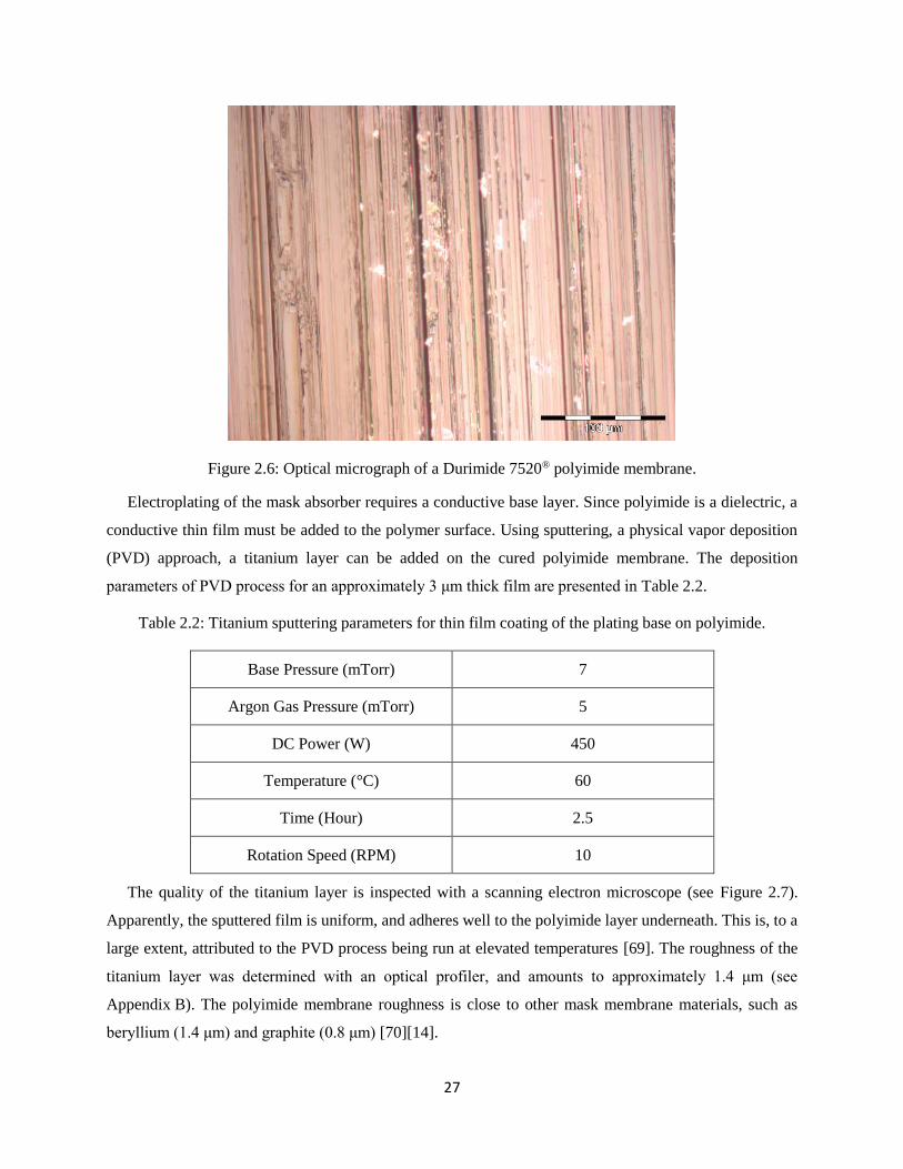
27
Figure 2.6: Optical micrograph of a Durimide 7520® polyimide membrane.
Electroplating of the mask absorber requires a conductive base layer. Since polyimide is a dielectric, a
conductive thin film must be added to the polymer surface. Using sputtering, a physical vapor deposition
(PVD) approach, a titanium layer can be added on the cured polyimide membrane. The deposition
parameters of PVD process for an approximately 3 μm thick film are presented in Table 2.2.
Table 2.2: Titanium sputtering parameters for thin film coating of the plating base on polyimide.
Base Pressure (mTorr) 7
Argon Gas Pressure (mTorr) 5
DC Power (W) 450
Temperature (°C) 60
Time (Hour) 2.5
Rotation Speed (RPM) 10
The quality of the titanium layer is inspected with a scanning electron microscope (see Figure 2.7).
Apparently, the sputtered film is uniform, and adheres well to the polyimide layer underneath. This is, to a
large extent, attributed to the PVD process being run at elevated temperatures [69]. The roughness of the
titanium layer was determined with an optical profiler, and amounts to approximately 1.4 μm (see
Appendix B). The polyimide membrane roughness is close to other mask membrane materials, such as
beryllium (1.4 μm) and graphite (0.8 μm) [70][14].

28
Figure 2.7: Scanning Electron Micrographs (SEMs) of the sputtered titanium layer on polyimide. Left:
overview at low magnification (the scale corresponds to 100 μm); Right: detailed close-up (the scale
corresponds to 3 μm).
The titanium layer is deliberately partially oxidized to prevent the natural dioxide from forming, which
is a dielectric. Formation of TiOx, x=1.9 is achieved by immersing the processed sample into an aqueous alkali
solution of sodium hydroxide (NaOH) and hydrogen peroxide (H2O2) at a temperature of 50°C.
Experiments have been performed to find an optimized process time of 25 seconds. If the oxidization time
is longer than designated, the titanium layer completely delaminates from the polyimide membrane. The
optimized finished sample appears as dark black, with a low electrical resistance of less than 3 Ω from
center to rim of the substrate.
2.5.2 Patterning of the Mask Absorber Templates
To fabricate the absorber structures on the polyimide membrane, a photoresist is spin-coated on the
titanium oxide layer, gets lithographically patterned by ultraviolet radiation, and the voids get filled with
metal structures using an electroplating process. A second spin-coating step is required to deposit 100 μm
of NR26-25000P® negative tone UV resist (Futurrex; Franklin, NJ). Spinning is performed at 720 RPM for
40 seconds. The resist is soft baked on a hotplate at 150°C for 450 seconds. The center block absorber
layout is transferred into the resist using a plastic film based UV mask and a mercury vapor lamp light. The
exposure dose was 2200 mJ/cm2. After a post-exposure bake of 90°C, the sample gets developed in 2.38%
tetramethyl ammonium hydroxide (TMAH) for 13 minutes at room temperature.
2.5.3 Electroplating of the Mask Absorber Structures
Based on the processing technology available in the laboratory at the time of the experiments, nickel
was selected as the absorber material for the test mask. Compared to gold absorber typically applied, thicker

29
absorber is required to guarantee complete absorption of the incident beam in the absorber. The nickel layer
target thickness is 80 μm.
The nickel electroplating bath SN-10 manufactured by Transene at Danvers, MA, consists of nickel
pellets in a titanium basket as the anode, and 4 liters of acidic sulfamate electrolyte containing organic
additives and wetting agents. The sample is immersed into the electrolyte as the cathode, maintaining a
parallel orientation and constant distance relative to the titanium basket. Using a precision constant current
source, nickel gets deposited onto the sample surface.
The electroplated nickel surface usually shows pitting. Pitting can be caused by many factors, such as
adhesion of air or hydrogen bubbles to the electroplating surface. Air bubbles should be removed from the
electrolyte by stirring. Pitting from adherent hydrogen bubbles can result from a solution that is chemically
out of balance, or is inadequately agitated. Further potential causes of pitting are low concentration of
wetting agents, the presence of organic contaminants and/or inorganic impurities, and incomplete cleaning
of the sample. By maintaining the composition of the electrolyte within specified limits, controlling the pH
value and temperature, and by preventing contaminations from entering the solution, pitting can be avoided
or reduced [71].
To deposit the nickel layer on the polyimide membrane, the sample is first cleaned with deionized water.
The electrolyte needs to be pre-heat to the working temperature of 50°C . A pH value of 4.2 to 4.8 is
maintained. The current density is set to 1 A/dm2, resulting in a deposition rate of 0.2 μm per minute. The
plating time for an 80 μm thick nickel layer therefore amounts to 400 minutes. The setup of the
electroplating bath is presented in Figure 2.8.
After electroplating, the NR26-25000P® resist template is entirely removed to increase the X-ray
transparency of the transparent mask areas. This stripping process is performed in Dimethyl Sulfoxide
(DMSO) for 5 minutes at 100°C.

30
Figure 2.8: Setup of nickel electroplating.
2.5.4 Etching of the Exposure Window and Gluing of the Mask Frame
The polyimide membrane is now patterned with absorber structures. It, however, could not be applied
as a mask yet since the steel substrate would absorb all incident X-rays. It needs to be removed as a
sacrificial substrate. In this case, rather than removing the entire wafer, an exposure window of 83 mm in
diameter was etched as this is regarded as the useful layout area. The outer rim of the steel substrate remains
as a support structure.
To create this 83 mm exposure window in the steel substrate, the wafer is chemically etched from the
backside. The etchant applied in this study is a 30% ferric chloride (FeCl3) solution. The outer backside rim
beyond the 83-mm-diameter is protected against unintentional etching by gluing on a self-adhesive tape.
At the edges of the tape, paraffin wax (ScholAR Chemistry; Rochester, NY) is used as a sealant. The
melting point of this wax is about 55°C , which is very close to the typical ferric chloride etchant
temperature of 50°C [72]. To avoid detachment of the sealant, the etching temperature is reduced to 40°C ,
at the cost of an increased etch time of 10 hours. 750 ml of fresh etchant are used for each process. After
etching of the window, turning the polyimide layer into a freely suspended membrane, the tape is removed
and the paraffin wax is dissolved in hot water. The remaining steel ring on the back side (see Figure 2.9) is
used as the interface to glue the mask frame.

31
Figure 2.9: Image of a processed mask (before gluing of the mask fame, view from the back side): the steel
ring (outer diameter 100 mm, inner diameter 83 mm, thickness 1.0 mm) remains after etching the exposure
window into the steel substrate. The orange-red color in the center stems from the polyimide membrane.
The mask frame is attached using a glue for metal bonding. This ensures best thermal contact and good
bond strength even at high temperatures. The glue applied is a two-component epoxy (J-B Weld; Atlanta,
GA), which takes one day to cure. The mask frame is 101.6 mm wide (4” format), while the mask membrane
is only 100 mm wide. Thus, the membrane will not get damaged when mounting in the scanner. At the
bottom side, the mask frame extends to 5” for precise mounting in the scanner mask adapter. The final
products of test masks are presented in Figure 2.10 and Figure 2.11.
Figure 2.10: Complete coverage test mask seen from the front side: the 80 μm thick nickel absorber covers
the entire mask area. The 5” outer diameter mask frame on the back side extends beyond the 4” mask area.

32
Figure 2.11: Center block test mask seen from the front side: the 80 μm thick nickel absorber covers the
square center block and the thin extension strip to protect the wires of the thermocouples (to be mounted
later) from X-ray exposure. The 5” outer diameter mask frame on the back side extends beyond the 4” mask
area.
2.5.5 Integration of the Individual Fabrication Steps into a Process Sequence
The fabrication steps discussed above can be integrated into a complete processing sequence:
1. Cleaning the stainless steel substrate with isopropanol and de-ionized water followed by an oxygen
plasma etch step;
2. Spin-coating of 30 μm Durimide 7520® polyimide resist on the steel substrate;
3. Soft baking of the polyimide resist;
4. Flood exposure of the polyimide resist with ultra-violet light, followed by post-exposure delay;
5. Curing of the polyimide resist;
6. Adding a 3 μm layer of titanium on the polyimide membrane by PVD;
7. Oxidizing the titanium layer to TiO1.9;
8. Spin-coating 100 μm NR26-25000P® negative tone UV-resist on the TiO1.9 layer;
9. Patterning the absorber template by UV-exposure with a film mask and development in 2.38% TMAH;
10. Electroplating of the absorber pattern with nickel sulafamate;
11. Stripping of the remaining NR26-25000P® resist in DMSO;

33
12. Etching of the exposure window from the backside of the steel substrate in 30% FeCl3 until the
membrane becomes freely suspended;
13. Bonding the test mask to mask frame using 2-component epoxy glue.
The critical steps are illustrated in the process flow diagram in Figure 2.12.
Figure 2.12: Fabrication sequence developed for polyimide X-ray masks at SyLMAND.
2.6 Chapter Summary
In this chapter, the selected properties of polyimide are further reviewed to determine the suitability of
the material as an X-ray mask membrane. Two polyimide products were experimentally studied: 1) P84®
polyimide solution from Evonik has been diluted with NEP solvent into a spincoatable polymer; 2)
Durimide 7520® is a photo-definable polyimide from Fujifilm. Both have been spincoated to examine the
quality of a thin film to eventually be used as the mask membrane. In the case of P84®, poor homogeneity
caused by air pockets prevented further use. For Durimide 7520®, a detailed fabrication sequence has been
developed to reliably produce polyimide thin films with the equipment available at SyLMAND. Stainless
steel wafers were selected as the sacrificial base substrate due to the high modulus in order to minimize
bending of the test mask during fabrication process. A 30 μm thick Durimide 7520® film was spincoated
onto the sacrificial substrate. TiO1.9 was then sputter-coated onto the polymer to be later used as the plating
base for electroplating the absorbers. On the plating base, 100 μm of UV-sensitive negative-tone resist

34
Futurrex NR26-25000P® were spin-coated and patterned by UV-exposure. The voids in this microstructure
were filled with 80 μm thick nickel, serving as the absorber in test masks. The polyimide film was finally
turned into a freely suspended membrane by locally removing the sacrificial steel wafer. An exposure
window of 83-mm-diameter was opened by etching the steel wafer with a 30% ferric chloride solution. As
the last fabrication step, the mask shim was bonded to a rigid mask frame using epoxy glue. Two test masks
were fabricated with this same fabrication sequence, but different layouts: one mask is completely covered
by absorbers; the second has an absorber layout of 42.4 mm side length square at the center, while the
remaining exposure window is transparent. The two test masks provided the basis for further experimental
and numerical studies.

35
CHAPTER 3
THERMAL AND THERMOELASTIC ANALYSIS OF THE POLYIMIDE MEMBRANE MASK
The heat load during X-ray exposure will determine the feasibility of a polyimide membrane X-ray mask
technology at SyLMAND. SyLMAND is equipped with an intensity chopper, which allows to reduce the
incident beam power, so that heat load in the mask and resist can be kept at acceptable levels. As a result,
the temperature rises in the mask as well as the thermal deformations will be reduced. In this chapter,
thermal and thermoelastic behavior of the test masks are studied by numerical methods, predicting the
temperature distributions and thermal deformations in the masks during exposure.
3.1 Modeling of the X-ray Exposure under Synchrotron Radiation
3.1.1 Simplifications and Assumptions in the Simulation Models
To simulate the heat load, the geometry of the exposure model is simplified as presented in Figure 3.1.
Photoresist and silicon wafer are not included in this model. The assembly of the test mask and the substrate
holder is reduced to a space of 140 mm × 140 mm × 18.2 mm. The helium-filled control volume is limited
to the proximity gap between substrate holder and mask holder, and to the exposure window of the mask
holder. The complex geometries of mask holder and substrate holder (compare with Figure 1.15) are
reduced to flat walls, with the proximity gap of 1.4 mm in-between. This a larger than typical proximity
gap distance, but will be necessary for subsequent experimental verification when thermocouples are placed
through the proximity gap. The extension segment protecting the thermocouple wires in the center block
mask is neglected for the simulations. The mask is simplified to a layer of nickel absorber on a polyimide
membrane, attached to the steel ring and aluminum mask frame. The x-y plane is the lateral plane, and z-
axis is the propagation direction of synchrotron beam. (see Figure 3.1)

36
Figure 3.1: Schematic of the simplified Finite Volume Method (FVM) model for thermal simulations: Left:
cross sectional view; Right: front view of the test mask, which is simplified to a layer of nickel absorber on
the polyimide membrane.
The helium pressure in the scanner working chamber during the exposure is 100 mbar. As the stage
scans through the chamber, the helium gas has a relative velocity with respect to the scanning stage, flowing
in the proximity gap between the X-ray mask and the substrate holder. The impact of this gas flow, resulting
dimensionless numbers, and a suitable boundary condition are derived based on the calculations of the fluid
dynamic properties for the helium in Appendix C. Continuum fluid mechanics with slip flow boundary
conditions where the relative velocity at the channel wall is non-zero would best be applied in the model.
However, the calculations of dimensionless numbers show that convection is not significant as the helium
gas flow is at a low velocity. Thus, not convection associated with the helium gas flow, but rather thermal
conduction is the dominant mode of heat dissipation in the proximity gap. To simplify the thermal
simulation, the slip flow condition is therefore neglected. Also, the reciprocating flow direction of helium
is simplified to be single directional.
The effective vertical beam height at the scanner is about 8.8 mm. The maximum width of the
synchrotron beam is 150 mm. It can be collimated by different slits in the beamline. In the case of the test
mask described in the previous chapter, the beam would get collimated to 83 mm by the mask frame, if not
cut upstream. It is therefore assumed that diligent sample preparations will ensure that the beam power is
not dissipated into the mask frame, but that slits upstream in the beamline collimate the beam to the useful

37
width. An incident beam width of 83 mm is therefore assumed as the worst case scenario, from a heat load
perspective, associated with the dimensions of the test mask.
The incident beam power is constant across the beam width, but varies with a Gaussian power profile in
the vertical direction. During exposure, the scanning process evens this vertical profile out to a
homogeneous energy deposition across the entire sample. In the simulations, the vertical power distribution
is therefore not modeled, but is represented by the corresponding incident power averaged over the 8.8 mm
by 83 mmm beam size. The incident beam power density is calculated using the software LEX-D developed
by Sandia National Laboratory, Livermore, USA (see Appendix D). It takes into account the storage ring
and beamline conditions, the stored electron current, as well as absorption in all beamline optical
components, the mask, and the sample. The data fed into the numerical model therefore deliver the values
for absorbed energies as the local heat sources in all relevant layers of the model. Figure 3.2 presents the
transmission of the mask components for the given spectral range: the polyimide membrane allows for good
transmission beyond 90% for relevant photon energies beyond 3 keV, and close to 100% for photon
energies of 5 keV and above. The nickel absorber, on the other hand, is almost entirely opaque to the
photons within the spectrum. It allows transmission of less than 10-3 for the energy spectral range, and a
maximum of 1% to 6% at selected spectral peaks. In blank membrane areas where there are no absorbers,
less than 10% of the locally incident beam power is deposited into the polyimide membrane, depending on
the exact exposure conditions. The remaining beam power gets transmitted through the membrane into the
sample and substrate holder where it is absorbed. Considering the heat transfer in the entire model, most of
the beam power gets absorbed in the mask absorber, from where it gets dissipated as heat through the entire
model. The model takes into account the various heat sources due to deposited beam power, regardless of
the location in the model.

38
Figure 3.2: X-ray transmission of the X-ray mask components from 1 to 15 keV [22].
The temperature distribution is simulated using the comprehensive model explained above, including
mask and substrate holders which impact the mask temperature. Thermal deformations are based on this
temperature distribution. Deformations of the holders, however, are neither expected in the cooled scanner
components, nor would they have an immediate impact onto the microstructures. The thermoelastic model
is therefore further reduced to the X-ray mask structure (see Figure 3.3). The bonds between the polyimide
membrane, nickel absorber, and the steel ring are considered to be rigid so that relative slip or twist will not
appear.
Figure 3.3: Schematic of the simplified mask model for thermoelastic simulations: Left: Back view of the
test mask, the steel ring constrains the polyimide membrane; Right: Front view of the simplified center
block mask.

39
3.1.2 Governing Equations and Boundary Conditions
A. Thermal simulation
To describe heat diffusion in a solid, the governing equation in a Cartesian system is
2 2 2
2 2 2
( )( , )
T T T T x, y,z,tk Q x, y,z t c
x y z t
(3.1)
where k is the thermal conductivity of the solid, ρ is the material density, c is the specific heat of the material,
Q is the heat generation rate, and T is the temperature [73].
The X-ray mask under synchrotron beam irradiation will be heated locally as energy gets deposited in
the absorber and in the membrane. In the case of the entirely nickel-covered mask, all beam power is
absorbed in the absorber (see Figure 3.4). To describe the heat diffusion in the X-ray mask, the governing
equations are
Figure 3.4: Schematic of the DXRL exposure model used in the simulation of the complete coverage mask:
Left: Exposure of the X-ray mask under synchrotron beam; Right: Heat generation in the absorber during
exposure.
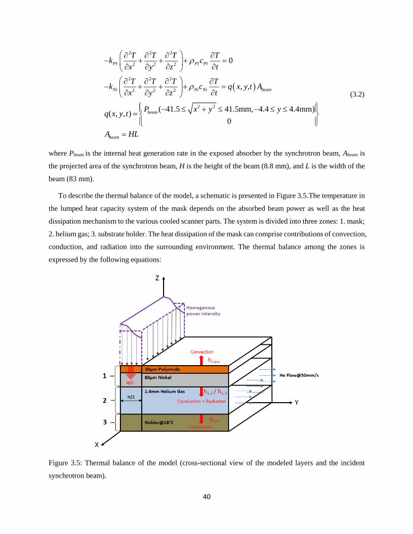
40
2 2 2
2 2 2
2 2 2
2 2 2
2 2
0
,
( 41.5 41.5mm, 4.4 4.4mm)( , , )
0
PI PI PI
Ni Ni Ni beam
beam
beam
T T T Tk c
x y z t
T T T Tk c q x y,t A
x y z t
P x y yq x y t
A HL
(3.2)
where Pbeam is the internal heat generation rate in the exposed absorber by the synchrotron beam, Abeam is
the projected area of the synchrotron beam, H is the height of the beam (8.8 mm), and L is the width of the
beam (83 mm).
To describe the thermal balance of the model, a schematic is presented in Figure 3.5.The temperature in
the lumped heat capacity system of the mask depends on the absorbed beam power as well as the heat
dissipation mechanism to the various cooled scanner parts. The system is divided into three zones: 1. mask;
2. helium gas; 3. substrate holder. The heat dissipation of the mask can comprise contributions of convection,
conduction, and radiation into the surrounding environment. The thermal balance among the zones is
expressed by the following equations:
Figure 3.5: Thermal balance of the model (cross-sectional view of the modeled layers and the incident
synchrotron beam).

41
11 1 1 1,3 1 1,2 1 1 0
22 2 2 1,2 1 2 2,3 3 2
1 1
1
( ( ) ( )
( ) ( )
@ uncovered area @ uncovered area,
@covered area @covered area
,
beam 3 1 2
PI PI
Ni Ni
Niconv 1,2
dTcV q(t)A Ah T -T )- Ah T -T Ah T T
dt
dTc V Ah T -T Ah T -T
dt
cc
c
k kh h h
3
3 13 1 0 2 3
2 1 3 2
, 4 ,He He Steel1, ,
Ni He He Steel
k kh F T h
k D k D k D k D
(3.3)
where A is the area of exposure, D is the thickness for each layer, h is the heat transfer coefficient for each
layer (h1 is between the mask and helium gas in the exposure window, h1,2 is between the mask and helium
gas in the proximity gap, h1,3 is between the mask and the substrate holder, h2,3 is between helium gas in the
proximity gap and the substrate holder), F is the view factor of radiation (in this case F13 is 1), ε is the
emissivity of absorber (0.11 for nickel [74]), σ is the Stefan-Boltzmann constant (5.67∙10-8 W/m2/K4), and
T0 is the background temperature of 18°C [75].
B. Thermoelastic simulation
The basic equations of elasticity for the homogenous and isotropic material per unit volume under the
internal body forces are (see Figure 3.6)
Figure 3.6: Components of stress in three dimensions.
dy
dx
dz

42
..
..
..
yxxx zx
xy yy zy
yzxz zz
X ux y z
Y vx y z
Z wx y z
(3.4)
where σ is the Cauchy stress tensor (normal stresses: σxx , σyy , σzz ; shear stresses: σxy , σxz , σyx , σyz , σzx , σzy),
X, Y, and Z are the internal body forces, and the second order derivatives of u, v, and w are the accelerations
in Cartesian coordinates [76].
The relationship between strain, displacement, and stress is given by the Hooke’s law as
0
0
0
1
1
1
2
2
2
xx xx yy zz
yy yy zz xx
zz zz xx yy
xy
xy
yz
yz
zxzx
uT T
x E
vT T
y E
wT T
z E
v u
x y G
w v
y z G
u w
z x G
(3.5)
where ε in the strain tensor, υ is the Poisson’s ratio, α is the coefficient of thermal expansion (CTE), T-T0
is the temperature change, and G is the shear modulus [77].
For the thin structure in this study, the stresses in the vertical direction can be neglected. So the normal
and shear stresses along the z-axis are assumed to be zero as
0zz xz yz (3.6)
From Hooke’s law (compare to 3.5)
0
0
( )
xz yz
zz xx yy T TE
(3.7)

43
The steel ring of the test mask is regarded as a rigid physical constraint, where the deformation of the
mask structure is zero within the bonding area with the mask frame.
To compare the stress distribution of various nodes in the model, the equivalent stress (von-Mises stress)
is defined as
1/222 2 2 2 2 26
2
xx yy yy zz zz xx xy yz zx
e
(3.8)
3.2 Simulations
The commercial numerical analysis software package used in this study is ANSYS R14.5. The model
developed in this study divides the simulation in two steps which involve a different discretization as stated
above, and also different ANSYS components: the temperature distribution in the test masks during the
transient conditions of the scanned exposure are solved with the computational fluid dynamics software
ANSYS FLUENT® for each time step of the considered scanning process using the finite volume method
(FVM). Based on these temperature distributions, the thermoelastic stresses and the deformations are
determined by ANSYS Mechanical® using the finite element method (FEM), focusing on the maximum
temperature rises at thermocouples in the mask.
3.2.1 Meshing of the Model
The models need to be meshed separately for the thermal and the thermoelastic simulation due to the
different numerical methods involved. The X-ray mask consist of comparatively thin membrane (30 μm)
and absorber (80 μm), but a 1,250 or 3,333 times larger lateral dimension (100 mm). To keep the number
of elements in the mesh at a manageable level for computer, and to ensure the maximum aspect ratio in any
given mesh cell does not exceed 100:1 (cells no more than 100 times wider than thick in this case) so that
the results converge well and remain accurate, single layer of elements will be generated in each of these
two zones.
The mesh for the thermal simulation applying the FVM was built by the software GAMBIT®. The mesh
is a conformal grid solely consisting of quadrilateral cells. The FEM mesh for the thermoelastic simulation
was built by ANSYS Meshing®, covering only the test masks themselves. Most elements are 20-node
cuboids referred to as Hex 20, while a few elements are 15-node prisms referred to as Wed 15. The two
types of element are simultaneously identified as Solid 186 in ANSYS Mechanical® (see Figure 3.7).

44
Complete information on the four meshes used for the thermal FVM and the thermoelastic FEM model
for both the test masks are presented in Table 3.1. The thermal and thermoelastic properties of the materials
in the simulations are presented in
Table 3.2.
Figure 3.7: Left: FEM mesh of the complete coverage mask for the thermoelastic simulation; Right: details
of the FEM elements used in the mesh.
Table 3.1: Overview of mesh sizes and properties.
Test Mask Simulation Mode Nodes
[×103]
Elements
[×103] Max. Aspect Ratio
Complete Coverage
FVM (thermal) 1,586 1,421 84.6
FEM (thermoelastic) 184 258 50.5
Center Block
FVM (thermal) 1,059 940 84.6
FEM (thermoelastic) 422 638 54.8

45
Table 3.2: Thermal and mechanical material properties used in the simulations [67]
Material Thickness
(mm)
Density
(kg/m3)
Specific
Heat
(J/kg)
Thermal
Conductivity
(W/m/K)
Coefficient
of Thermal
Expansion
(K-1)
Young’s
Modulus
(GPa)
Poisson’s
Ratio
Aluminum 8 2719 871 202.4
Polyimide 0.03 1420 1080 0.2 55.0e-6 2.5 0.34
Nickel 0.08 8900 460.6 91.7 13.4e-6 200 0.31
Helium 1.4 0.01652 5193 0.1507
Stainless
Steel
1.0 (steel
ring)
5.0 (substrate
holder)
7750 502.5 16.3 17.0e-6 193 0.31
3.2.2 Thermal Simulations
The time step for the transient simulation is set to be 12.5 msec, which is close to the calculated time
step in Appendix C. The simulation flow time is 20 seconds. This corresponds to the typical duration from
the start of the exposure process until the temperature distribution in the mask reaches a steady state, i.e.
does not further increase from scan to scan. The initial temperature of the model is 18°C . Incident beam
powers are selected from the experiments in Chapter 4, one for either test mask. The beam power density
locally absorbed in the absorber or in the open areas of the polyimide membrane (in the case of the center
block) as obtained from LEX-D is converted to an equivalent internal heat generation in the nickel absorber.
The internal heat generation is implemented in ANSYS FLUENT® as a User Defined Function (UDF)
program written in the program language C. The UDF program template is presented in Appendix E. The
initial position of the synchrotron beam is assumed to be at the center of the mask. The helium gas flow
enters the model from the bottom and from the vertical boundary planes of the model at a speed of 50 mm/s.
This is also the scan speed with which the beam moves vertically up and down the model for a stroke length
of 75 mm.

46
The time-resolved simulated temperatures at the positions where the five thermocouples are placed on
the absorber surface in the corresponding experiments (see Figure 4.2 in Chapter 4) are presented for both
test masks. #5 is in the center of the mask, #1 to #4 are at half radius, at 9, 12, 3, and 6 o’clock respectively.
Furthermore, the local temperature distribution in the mask at the time when the maximum temperature is
simulated in any one of the five thermocouple locations is shown. Due to the symmetricity of thermocouple
installation, the simulated temperature distribution of thermocouple #2 in the top of the mask will be
presented while thermocouple #4 in the bottom is neglected. Thermocouple #5 at the center of the mask is
collinear with #1 and #3 in the horizontal direction, where the maximum temperature at these positions will
appear at the same time.
A. Complete coverage mask
In the first simulation, a beam power of 16.86 W impinges onto the model (compare experimental test
#6 for the complete coverage mask) representing the case of white-light exposure (without mirrors) at
233.2 mA electron current, 30 μm aluminum and 150 μm Kapton® X-ray pre-absorbers, and 25% open duty
cycle of the chopper. This corresponds to a beam power of Pbeam = 23,223 W/m2. The simulated
temperatures at the five thermocouples positions are presented in Figure 3.8. The temperature distribution
after 19.0 seconds when the beam is located at the center of the mask and the maximum temperature
appeared at the center thermocouple #5, and after 16.4 seconds when the beam is located at thermocouple
#2, are presented in Figure 3.9 and Figure 3.10.
Figure 3.8: Simulated temperatures with respect to flow time at the locations where the five thermocouples
are placed in the experiments for the complete coverage mask.

47
Figure 3.9: Simulated temperature distribution when the beam is at the location of the top thermocouple
(#2) and the temperature reaches its highest values in that location. Simulation for the complete coverage
mask.
Figure 3.10: Simulated temperature distribution when the beam is at the location of the center thermocouple
(#5) and the temperature reaches its highest values in that location. Simulation for the complete coverage
mask.

48
B. Center block mask
In the second set of simulations, a beam power of 17.24 W impinges onto the model (compare
experimental test #6 for the center block mask) representing the case of white-light exposure (without
mirrors) at 238.4 mA electron current, 30 μm aluminum and 150 μm Kapton® X-ray pre-absorbers, and 25%
open duty cycle of the chopper. This corresponds to a beam power of Pbeam = 23,747 W/m2. The simulated
temperatures at the five thermocouples positions are presented in Figure 3.11. The temperature distribution
after 19.0 seconds when the beam is located at the center of the mask and the maximum temperature
appeared at the center thermocouple (#5), and after 16.4 seconds when the beam is located further up, at
thermocouple #2, are presented in Figure 3.12 and Figure 3.13.
Figure 3.11: Simulated temperatures with respect to flow time at the locations where the five thermocouples
are placed in the experiments for the center block mask.

49
Figure 3.12: Simulated temperature distribution when the beam is at the location of the top thermocouple
(#2) and the temperature reaches its highest values in that location. Simulation for the center block mask.
Figure 3.13: Simulated temperature distribution when the beam is at the location of the center thermocouple
(#5) and the temperature reaches its highest values in that location. Simulation for the center block mask.

50
3.2.3 Thermoelastic Simulations
The temperature distributions in the test masks obtained from thermal simulations are transferred into
the FEM models for thermoelastic simulations of temperature-induced thermal deformations and stress.
The total deformation of the mask structure (the vector addition of deformations in the Cartesian
coordinates), the deformations in each axis, and the equivalent stress are presented in Table 3.3.
Table 3.3: Maximum temperature at different thermocouple positions from thermal simulation
Mask Thermocouple ID Flow Time (sec) Temperature (°C)
Complete Coverage
#2 16.4 39.46
#5 19.0 38.75
Center Block
#2 16.4 37.71
#5 19.0 37.07
A. Complete coverage mask
The thermoelastic simulation results for the complete coverage mask are presented in Figure 3.14 to Figure
3.18.
Figure 3.14: Simulated total (3-dimensional) deformations (in micrometers) for the complete coverage
mask: Left: Deformations when the beam is at the location of the top thermocouple (#2); Right:
Deformations when the beam is at the location of the center thermocouple (#5).

51
Figure 3.15: Simulated deformations (in micrometers) in the lateral plane along the x-axis (orthogonal to
the incident synchrotron beam) for the complete coverage mask: Left: Deformations when the beam is at
the location of the top thermocouple (#2); Right: Deformations when the beam is at the location of the
center thermocouple (#5).
Figure 3.16: Simulated deformations (in micrometers) in the lateral plane along the y-axis (orthogonal to
the incident synchrotron beam) for the complete coverage mask: Left: Deformations when the beam is at
the location of the top thermocouple (#2); Right: Deformations when the beam is at the location of the
center thermocouple (#5).

52
Figure 3.17: Simulated deformations (in micrometers) along the z-axis (along the beam direction,
orthogonal to the lateral plane) for the complete coverage mask: Left: Deformations when the beam is at
the location of the top thermocouple (#2); Right: Deformations when the beam is at the location of the
center thermocouple (#5).
Figure 3.18: Simulated equivalent stress distributions (in MPa) for the complete coverage mask: Left:
Deformations when the beam is at the location of the top thermocouple (#2); Right: Deformations when the
beam is at the location of the center thermocouple (#5).

53
B. Center block mask
The thermoelastic simulation results for the center block mask are presented in Figure 3.19 to Figure 3.23.
Figure 3.19: Simulated total (3-dimensional) deformations distributions (in micrometers) for the center
block mask: Left: Deformations when the beam is at the location of the top thermocouple (#2); Right:
Deformations when the beam is at the location of the center thermocouple (#5).
Figure 3.20: Simulated deformations (in micrometers) along the x-axis (orthogonal to the incident
synchrotron beam) for the center block mask: Left: Deformations when the beam is at the location of the
top thermocouple (#2); Right: Deformations when the beam is at the location of the center thermocouple
(#5).

54
Figure 3.21: Simulated deformations (in micrometers) along the y-axis (orthogonal to the incident
synchrotron beam) for the center block mask: Left: Deformations when the beam is at the location of the
top thermocouple (#2); Right: Deformations when the beam is at the location of the center thermocouple
(#5).
Figure 3.22: Simulated deformations (in micrometers) along the z-axis (along the beam direction,
orthogonal to the lateral plane) for the center block mask: Left: Deformations when the beam is at the
location of the top thermocouple (#2); Right: Deformations when the beam is at the location of the center
thermocouple (#5).

55
Figure 3.23: Simulated equivalent stress distributions (in MPa) for the center block mask: Left:
Deformations when the beam is at the location of the top thermocouple (#2); Right: Deformations when the
beam is at the location of the center thermocouple (#5).
3.3 Discussion
The results for the temperature distribution at the five thermocouple positions as a function of time
(Figure 3.8 and Figure 3.11) show that after three full scans, the steady state temperatures are reached and
further increase from scan to scan is at best minimal. Whenever the beam passes a simulated spot, the
temperature increases immediately, and slowly decreases due to heat transfer to the cooled parts, until the
beam exposes the same area again, in the next scan. The three locations across the half-height line of the
mask (thermocouples #1, #3, and #5) show a series of identical temperature changes. The top thermocouple
(#2) reaches its highest value shortly before the center ones, the bottom thermocouple (#4) shortly after the
center one (#5). The temperature patterns for the top and bottom location are not identical for each spot.
The fact that close to the top or bottom, the reverse point of the scan is close, two temperature rises are
shortly separated in space, followed by a relatively longer cooling period until the beam scanned all the
way back. Due to the double-exposure without much dwell in between, the top and the bottom
thermocouples reach the highest temperature in the models. The center thermocouple (#5) location gets
hotter than the ones on the sides at half height since the path to the cooled scanner components on the outer
rim of the mask is farther away: Overall, the highest temperature during exposure of about 37°C to 40°C
does not appear at the center of the mask, but at the two symmetrical positions at the top and bottom of the
mask where thermocouples #2 and #4 are installed. This is because the scanning speed is faster than the
heat dissipation speed, which leads to a distinct boundary between the exposed and unexposed area during
the scanning process. The slow heat dissipation also explains the overlap of the temperature distribution

56
profile and the equivalent stress profile in the complete coverage mask (compare Figure 3.9, Figure 3.10,
and Figure 3.18), which the accumulation of local heat causes larger local deformations.
The temperature distribution strongly depends on the position of synchrotron beam. Figure 3.9, Figure
3.10, Figure 3.12, and Figure 3.13 indicate the maximum temperature rises at the line that represents the
current position of the beam. In all the figures here, the beam is scanning downwards, as can be seen from
the comparatively cool area below the current beam position, and the slowly decreasing temperature above.
The temperature distribution also depends on the absorber layout: the heat dissipation of the center block
is through conduction across the proximity gap, while the energy deposited in the absorber of the complete
coverage mask can also be laterally transferred through the metal absorber to the mask frame by thermal
conduction. In the second case, heat transfer across the polyimide membrane to the steel ring acts as a
thermal barrier. Besides, the increased heat transfer capability is counteracted by the fact that more heat is
absorbed in this complete coverage absorber. Ultimately, both masks lead to similar maximum temperatures.
This might change if conduction across the proximity gap becomes less effective. During actual
exposures, silicon wafers are coated with resists that also feature low thermal conductivity, such that the
resist surface temperature will increase instead of the constant temperature modeled here in the substrate
holder. On the upside, though, would a typical proximity gap would be 100 μm rather than 1.4 mm (which
had to be chosen to accommodate thermocouples in the actual experiments), which would enhance the
cooling effectiveness across the proximity gap significantly.
The total deformations in the test masks are mostly attributed to the axial deformations in the z-axis. The
deformations in the lateral plane for complete coverage mask are approximately 6% of the deformations in
the axial direction: up to 2 μm along the x-axis (see Figure 3.15) and 4 μm along the y-axis (see Figure
3.16). The deformations in the lateral plane for center black mask are approximately 20% of the
deformations in the axial direction: up to 13 μm along the x-axis (see Figure 3.20) and 10 μm along the y-
axis (see Figure 3.21). The axial direction deformation needs to be controlled within the distance of the
proximity gap, so the absorber structures will not contact with the photoresist.
The thermal deformations in the test masks are affected by two factors. First, the thermal expansion
coefficient is much higher for polyimide than it is for nickel, which leads to stronger expansion in the mask
membrane compared to the absorber structure at a given temperature. Secondly, temperatures are even
anticipated to increase: the thermal conductivity of polyimide is much lower than that of other potential
materials for mask membranes, i.e. ceramics and metals. The heat dissipation by thermal conduction to the
mask frame therefore is less efficient for a polyimide membrane, which often causes a relatively higher
temperature in large isolated absorber structures. Although the temperature rise in the center block mask is
lower than in the complete coverage mask, the deformations in all directions are larger in the center block

57
mask. This is because the modulus of polyimide is much lower than for nickel, such that the polyimide
membrane around the center absorber can more easily get distorted. Considering that typical mask layouts
will rarely feature large areas without structural support from mask absorbers, the complete coverage mask
should better represent the thermal deformations.
The deformation in the complete coverage mask is determined by the temperature distribution in the
mask since there is no lateral variation in material composition. During the exposure, the maximum
deformation moves along with the synchrotron beam (see Figure 3.14). As the steel ring constrains the
mask in the lateral plane, the deformation of the mask structure will be afferent, forming a spherical
deflection out of the lateral plane in axial direction (z-axis) (see Figure 3.22). This out-of-plane deformation
along the beam direction is up to about 20 μm for a scan position close to the top (see Figure 3.17, left),
and can add up to about 40 μm for a central scan position (see Figure 3.17, right) which constitutes a worst
case of thermal deformation. Such deformations along the beam direction are not necessarily problematic
since the angle between the lateral plane and the deflected membrane are still extremely small. This way,
no adverse impact of tilted mask absorber could be occurring. More problematic would be deformations
within the lateral plane. They are limited, though, to only 2 μm along the x-axis (see Figure 3.15) and 3 μm
along the y-axis (see Figure 3.16). Furthermore, as the beam scans reciprocally in the vertical direction, the
deformation in horizontal direction is symmetric (see Figure 3.15), while the deformation in vertical
direction depends on the position of synchrotron beam (see Figure 3.16).
The deformation in the center block mask depends on the temperature distribution, as similar results are
obtained compared with complete coverage mask. An additional effect, though, is that the outline of the
absorber structures coincides with sharp changes of the temperature, comparable to the temperature change
at the mask rim in the case of the complete coverage mask. Furthermore, the mechanical properties change
significantly at the absorber edges and corners, causing local stress concentrations, so that these structures
can be detected in stress, strain and deformation plots even when there are limited temperature gradients
driving thermal stress (see Figure 3.23). To provide a schematic overview, the layout of the center block
absorber can be represented by a 5×5 grid, where local deformations at each point in the grid are presented
to get a better understanding (see Figure 3.24).

58
Figure 3.24: 3D schematic of the center block absorber deformation when the beam is at the location of the
center thermocouple (#5): Blue: original absorber layout; Red: deformed absorber layout (deformation
scaled by 200).
To quantify the effect of the intensity chopper, the temperature in the complete coverage mask has been
simulated again at the same conditions as before, but without the 25% open duty cycle intensity chopper.
This means that in this case, the incident beam power is four times higher than before: With chopper, the
temperature increased by 22°C from 18°C to about 40°C. Without an intensity chopper, the increase in
temperature reflects the increase in power and now is about four times higher, by 83°C from 18°C to 101°C
(see Figure 3.25). In this case, the thermal deformations of the mask are increased to four times of the value
observed at 25% duty cycle (see Figure 3.26). The deformation in the axial direction is about 160 μm, which
is far beyond the standard proximity gap of 100 μm and would lead to direct contact between the mask and
resist during exposure. This result suggests that without the intensity chopper, polyimide X-ray masks
would not be applicable at SyLMAND.

59
Figure 3.25: Simulated temperature distribution after 19.0 seconds when the beam is at the location of the
center thermocouple (#5) and the temperature reaches its highest values in that location. Simulation for the
complete coverage mask, exposure without intensity chopper implementation.

60
Figure 3.26: Simulated deformations (in micrometers) for the complete coverage mask, exposure without
intensity chopper implementation: Upper Left: Total deformation; Upper Right: Deformation along the x-
axis; Lower Left: Deformation along the y-axis; Lower Right: Deformation along the z-axis.
3.4 Chapter Summary
In this chapter, a consistent numerical model was developed based on the FVM and the FEM. The
software package ANSYS R14.5 was used for a two-stepped approach: The temperature distributions in
the test masks during were simulated with the FVM based fluid dynamics module ANSYS FLUENT® for
each time step of the considered scanning processes. Based on the obtained temperature distribution, the
thermoelastic stress and deformations were determined by ANSYS Mechanical® using the FEM. One case
considered for either mask, with input data calculated in the software LEX-D. Discussions of simulation
results focused on the maximum temperature rises obtained for those locations that were later
experimentally verified by five thermocouples on the mask. The results show that, for the load cases
considered, both masks reach comparable maximum temperatures of about 37°C to 40°C. The highest

61
temperatures are not observed at the exact center of the mask, but rather off towards the top or bottom
where there is less time to cool back down between two subsequent X-ray exposures during the scan process.
The resulting thermal deformations in the test masks are largest in the axial direction along the incident
beam. In the lateral plane, however, the deformations for the complete coverage mask are only
approximately 6% of the deformations in axial direction and amount to 2 μm along the x-axis and 4 μm
along the y-axis. The deformations in the lateral plane for center black mask are approximately 20% of the
deformations in axial direction: Up to 13 μm along the x-axis, and 10 μm along the y-axis. The intensity
chopper was proven to reduce the head load proportionally to its open duty cycle, i.e. ¼ of the temperature
rise at 25% duty cycle with respect to full beam power. This is critical for maintaining acceptable
temperature rises, and therefore deformations, during DXRL exposures as discussed in Chapter 5.

62
CHAPTER 4
THERMAL MEASUREMENTS OF POLYIMIDE MEMBRANE MASKS AND VERIFICATION OF
THERMAL SIMULATIONS
4.1 Experimental Design and Setup
4.1.1 Properties of the Synchrotron Beam
The geometry of the synchrotron beam can be adjusted by slits in the beamline and apertures in the
scanner. The beamline slits are set to 7 mm in height, basically admitting the entire beam. At the scanner,
the vertical aperture is set to 100 mm so the entire mask can get exposed when scanned through the beam.
At the sample location, the effective vertical beam height was measured with X-ray sensitive paper to be
approximately 8.8 mm according to the vertical opening angle of 0.52 mrad [46]. Horizontally, the beam is
collimated to 83 mm in the scanner just upstream the mask frame. This allows to expose the entire exposable
area of the test masks, which is 83 mm in diameter.
The beam profiles can be studied by fly-wire photocurrent detection systems in the double mirror system
[46]. Figure 4.1 shows the vertical beam profile at the mirror entrance with about 7 mm beam height
(between 16.8 mm and 23.8 mm relative height in this graph), exhibiting a Gaussian distribution.
Figure 4.1: Vertical beam profile scanned with the fly-wire photocurrent measurement system at the mirror
entrance. The beam is collimated to 7 mm using the upstream slits.

63
During the experiments, the intensity chopper is usually set to 25% open duty cycle, i.e. it cuts 75% of
the original beam power. The mirrors are retracted such that they do not modify the spectral or power
distribution. In the scanner, pre-absorbers are installed to further decrease the incident beam power: 30 μm
aluminum and 150 μm Kapton®. The exposures take place at a stored electron current of about 220 mA.
4.1.2 Exposure Parameters
Test exposures can be fairly short as thermal equilibrium is reached for less than 1 minute. The scanner
was programmed with dose expenditures equivalent to around three-minute exposure time.
With the beamline parameters kept constant, the only remaining variable impacting the incident beam
power is the stored electron current. The current decays quasi-exponentially. To calculate the incident beam
power and relate the experimental results to this beam power, the actual beam current must therefore be
recorded for every test exposure.
To investigate the temperature of the test masks as a function of the beam power with otherwise constant
conditions, the experiments are repeated for various beam currents. Besides, the intensity chopper is applied
to reduce the beam power (or simulate much smaller beam currents) during some tests, with settings of both
10% and 25% open duty cycle.
All experiments are done at a scan speed of 50 mm/s with a scan height of 75 mm. Before and after each
scan stroke, the scanner stage accelerates or decelerates at 400 mm/s2.
Photoresist and silicon wafer are not loaded in the scanner during the experiments. The reason is that
only a limited distance is available between the mask plane and the substrate holder. Almost the entire
allowance is used up by the proximity gap to accommodate the thermocouples. Further elements, such as a
sample silicon wafer with resist, cannot be added. During the experiments, the bare substrate holder
therefore faces the mask.
4.1.3 Experimental Setup with Thermocouples
In this study, the temperature is measured by thermocouples that are placed behind mask absorbers to
protect them from direct synchrotron exposure and related unwanted additional heating due to absorption
of radiation. The thermocouples are brought in close thermal contact with the mask absorbers by pressing
them against the absorbers using self-adhesive Kapton® tape. The 1 m-long American Wire Gauge 40, PFA-
coated wires are protected from synchrotron exposure by mask absorbers or a small nickel extension from
the center absorber to the mask frame in the case of the center block mask. The thermocouples used in the
experiment are chromel/alumel (K-type) 5SC-TT-K-40-36 from Omega Engineering (Stamford, CT, USA).
The thermocouples have a wire diameter of 76 μm.

64
Five thermocouples are used to measure the temperature rise in the exposed area of the test masks. They
are placed at the center (#5) and at half distance of the mask radius in both, vertical and horizontal directions
(#1-#4, ordered in a clock-wise, with #2 at the top). Figure 4.2 illustrates the positions.
Figure 4.2: Schematics of the positioning of the five thermocouples on the test masks. Left: Complete
coverage mask; Right: Center block mask.
The thermocouples are connected to a data acquisition device through a small flange DN40 vacuum port
on the wall of the scanner working chamber. The sampling frequency is 8 Hz for the measurement.
Figure 4.3 and Figure 4.4 show the experimental setup, consisting of the test masks mounted in the mask
holder of the scanner, as well as five thermocouples mounted to the mask absorbers.
Figure 4.3: Experimental setup of the complete coverage mask, mask holder, scanner adapter, and five
thermocouples.

65
Figure 4.4: Experimental setup of the center block mask, mask holder, scanner adapter, and five
thermocouples.
4.2 Experimental Results
The temperatures of the thermocouples mounted onto the test masks are measured under different
exposure conditions. During a specific experiment, the incident beam power linearly decreases with the
decaying electron current. A typical exposure lasts for a few minutes. During this time, the current typically
decays by less than 0.1%. The arithmetic average of the beam currents at beginning and end of the exposure
is therefore used to represent the beam condition for each test with sufficient precision. The incident beam
power density for each case is calculated by the LEX-D software. In this way, the incident beam power
across the exposed area of 83 mm by 8.8 mm can be calculated for comparison of the experimental results
with the numerical simulations of comparable cases.
Detailed measurement results are presented in Appendix F. Key results are listed below. Table 4.1 and
Table 4.3 summarize the actual exposure conditions for each experiment, including the calculated incident
beam power. Table 4.2 and Table 4.4 extract the highest temperatures that occurred for each experiment at
each thermocouple.

66
4.2.1 Test Results for the Complete Coverage Mask
Table 4.1: Exposure parameters for the complete coverage mask.
Test # Beam Current
(mA)
Incident Beam
Power
(W)
calculated by
LEX-D
Pre-absorbers
Insertion
(30 μm Al,
150 μm
Kapton)
Intensity Chopper
Open Duty Cycle
1 218.5 6.32 Y 10%
2 235.5 11.91 N 10%
3 178.2 12.89 Y 25%
4 202.6 14.65 Y 25%
5 219.6 15.88 Y 25%
6 233.2 16.86 Y 25%
7 222.3 28.10 N 25%
Table 4.2: Maximum temperatures measured by thermocouples on the complete coverage mask.
Test
#
Incident Beam
Power
(W)
calculated by
LEX-D
Maximum
Temperature
of #1
(°C)
Maximum
Temperature
of #2
(°C)
Maximum
Temperature
of #3
(°C)
Maximum
Temperature
of #4
(°C)
Maximum
Temperature
of #5
(°C)
1 6.32 23.30 23.02 22.08 24.52 23.59
2 11.91 27.05 26.90 25.24 30.18 28.04
3 12.89 27.86 27.80 26.07 31.36 28.78
4 14.65 29.92 30.72 28.54 33.72 30.97
5 15.88 30.08 30.09 27.77 34.23 30.87
6 16.86 31.78 32.65 31.33 35.82 32.67
7 28.10 38.47 38.43 34.35 46.57 40.86

67
4.2.2 Test Results for the Center Block Mask
Table 4.3: Exposure parameters for the center block mask.
Test # Beam Current
(mA)
Incident Beam
Power
(W)
calculated by
LEX-D
Pre-absorbers
Insertion
(30 μm Al,
150 μm
Kapton)
Intensity Chopper
Open Duty Cycle
1 214.3 6.20 Y 10%
2 210.6 10.65 N 10%
3 182.6 13.13 Y 25%
4 188.8 13.65 Y 25%
5 206.2 14.91 Y 25%
6 238.4 17.24 Y 25%
7 207.7 26.25 N 25%
Table 4.4: Maximum temperatures measured by thermocouples on the center block mask.
Test
#
Incident Beam
Power
(W)
calculated by
LEX-D
Maximum
Temperature
of #1
(°C)
Maximum
Temperature
of #2
(°C)
Maximum
Temperature
of #3
(°C)
Maximum
Temperature
of #4
(°C)
Maximum
Temperature
of #5
(°C)
1 6.20 23.07 22.46 22.88 24.46 24.29
2 10.65 26.19 25.06 25.69 28.51 28.12
3 13.13 28.13 27.22 27.61 30.61 30.03
4 13.65 28.88 27.43 28.79 31.83 30.48
5 14.91 29.45 28.33 28.76 32.36 31.80
6 17.24 31.81 29.87 31.24 34.79 33.90
7 26.25 37.91 35.81 36.76 42.89 42.18

68
4.3 Interpolation of the Temperature Rise as a Function of the Incident Beam Power
To generalize the results of the thermal study, the dependency of relevant temperatures is derived as a
function of the incident beam power. Subsequently, the measured maximum temperatures at the center of
the test masks from Table 4.2 and Table 4.4 are plotted as a function of the incident beam powers. Figure
4.5 and Figure 4.6 show a proportional relationship for both of the complete coverage and the center block
mask. The validation of the relationship between mask temperature and incident beam power strongly
depends on the distance of the proximity gap. As the distance becomes smaller, the better heat transfer
through the proximity gap will further reduce the temperature in the masks during exposure.
The linear fit shows that thermal conduction, which linearly relate heat transfer and temperature,
dominates the heat transfer mechanism. The functions obtained from the curve fitting suggest that the center
block mask has a higher temperature compared to the complete coverage mask at the same incident beam
power. The slope ratio of the fitted functions for the two cases is 9:8. This finding is consitent with simulated
results: The energy deposited in the complete coverage mask is triple of it is in the center block mask, since
the area of its nickel layer is two times larger. However, the lower thermal conductivity of polyimide
compared to nickel results in a less efficient dissipation of heat in the center block mask, such that despite
of the reduced beam power absoprtion, almost identical temperatures are observed.
Figure 4.5: Maximum temperature at the center thermocouple (#5) measured for various computed incident
beam powers with the complete coverage mask: curve fitting shows a linear relationship with a slope of
0.80°C /W for the complete coverage mask.
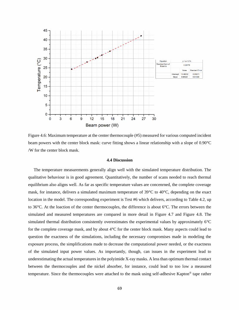
69
Figure 4.6: Maximum temperature at the center thermocouple (#5) measured for various computed incident
beam powers with the center block mask: curve fitting shows a linear relationship with a slope of 0.90°C
/W for the center block mask.
4.4 Discussion
The temperature measurements generally align well with the simulated temperature distribution. The
qualitative behaviour is in good agreement. Quantitatively, the number of scans needed to reach thermal
equilibrium also aligns well. As far as specific temperature values are concenrned, the complete coverage
mask, for instance, delivers a simulated maximum temperature of 39°C to 40°C, depending on the exact
location in the model. The corresponding experiment is Test #6 which delivers, according to Table 4.2, up
to 36°C. At the loaction of the center thermocouples, the difference is about 6°C. The errors between the
simulated and measured temperatures are compared in more detail in Figure 4.7 and Figure 4.8. The
simulated thermal distribution consistently overestimates the experimental values by approximately 6°C
for the complete coverage mask, and by about 4°C for the center block mask. Many aspects could lead to
question the exactness of the simulations, including the necessary compromises made in modeling the
exposure process, the simplifications made to decrease the computational power needed, or the exactness
of the simulated input power values. As importantly, though, can issues in the experiment lead to
underestimating the actual temperatures in the polyimide X-ray masks. A less than optimum thermal contact
between the thermocouples and the nickel absorber, for instance, could lead to too low a measured
temperature. Since the thermocouples were attached to the mask using self-adhesive Kapton® tape rather

70
than permanent, but thermally better conducting thermal glue, incomplete thermal contact might be a key
contributor to the slight offset in temperatures.
Figure 4.7: Simulated (solid line) and measured (dotted line) temperature with respect to time at the location
of the center thermocouple (#5) for the complete coverage mask.
Figure 4.8: Simulated (solid line) and measured (dotted line) temperature with respect to time at the location
of the center thermocouple (#5) for the center block mask.
A closer look at the temperatures measured at the top (#2) and bottom (#4) thermocouples reveals
unexpected results: in the simulations discussed in Chapter 3, both temperatures were identical, when
comparing the same case and at the time when the location is hit by the beam. This is a physically reasonable

71
result since the locations are thermally equivalent. The measured temperatures are different, though the
measured temperature at the bottom of the mask (#4) has the highest temperature rise and the top (#2) has
the lowest, rather than a symetrical temperature distribution in the vertical axis. The difference is about 6°C
in the case of complete coverage mask, and 4°C in the case of center block mask. The disparity between
the simulated and measured temperatures is attributed to an experimental artefact rather than a systematic
error in the simulations: during the experiments, the substrate holder was not maintained parallel to the
mask plane. The substrate holder is, under normal exposure conditions, pressed against the mask, using
proximity shims and maintaining parallel orientation. During the thermal tests, though, a much larger than
usual proximity gap was needed to accommodate the thermocouples, and proximity gap spacers could not
be used to protect the thermocouple wires. Under the given conditions, the substrate holder can slightly
swivel. Gravity leads to a slight tilting of the substrate holder, such that the proximity gap at the top is
smaller than at the bottom (see Figure 4.9). This leads to more efficient cooling across the smaller proximity
gap at the top, and hence lower temperatures: the proximity gap has an non-uniform distance so that the
thermal conductance of the helium gas is not homogenous at different heights.
Figure 4.9: Schematic of the tilted substrate holder during the measurements.
Apart from the mentioned minor discrepancies, the experiments basically validated the simulated model.
It can therefore be applied to simulate expected thermal distributions during the exposure process. In
Chapter 5, two typical DXRL exposure scenarios will be simulated.

72
4.5 Chapter Summary
In this chapter, the temperature distributions in the test masks during X-ray exposures were measured
with five thermocouples bonded to the absorber. For either of the two masks, seven different beam powers
were analyzed. Beam power adjusted by using different pre-absorbers and intensity chopper duty cycle
settings and were quantified by using the software LEX-D. For the complete coverage mask, maximum
temperatures of 24.5°C were measured for an incident beam power of 6.32 W, while a maximum
temperature of 46.6°C was recorded for an incident beam power of 28.1 W. For the center block mask,
maximum temperatures of 24.5°C were measured for an incident beam power of 6.20 W, while a maximum
temperature of 42.9°C was recorded for an incident beam power of 26.3 W. While the experimental results
generally validate the numerical results in the preceding chapter, some discrepancies were found, which
were associated with an unexpected inconsistency in the experimental setup. Under the conditions required
for the experiments, the separation between mask and the substrate holder in the scanner during exposure
is not constant across the mask area, but varies locally and is therefore different from the constant value
assumed in the simulations. Fundamentally, however, the measured temperatures not only validated the
numerical cases considered before, but also proved that the temperature rise was proportional to the incident
beam power, which substantiated the target of becoming able to predict the temperature rise in the X-ray
mask for a wide range of potential load cases.
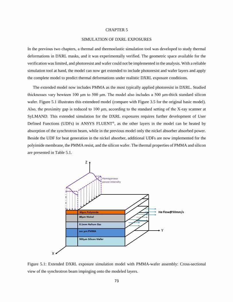
73
CHAPTER 5
SIMULATION OF DXRL EXPOSURES
In the previous two chapters, a thermal and thermoelastic simulation tool was developed to study thermal
deformations in DXRL masks, and it was experimentally verified. The geometric space available for the
verification was limited, and photoresist and wafer could not be implemented in the analysis. With a reliable
simulation tool at hand, the model can now get extended to include photoresist and wafer layers and apply
the complete model to predict thermal deformations under realistic DXRL exposure conditions.
The extended model now includes PMMA as the most typically applied photoresist in DXRL. Studied
thicknesses vary bewteen 100 μm to 500 μm. The model also includes a 500 μm-thick standard silicon
wafer. Figure 5.1 illustrates this extendeed model (compare with Figure 3.5 for the original basic model).
Also, the proximity gap is reduced to 100 μm, according to the standard setting of the X-ray scanner at
SyLMAND. This extended simulation for the DXRL exposures requires further development of User
Defined Functions (UDFs) in ANSYS FLUENT®, as the other layers in the model can be heated by
absorption of the synchrotron beam, while in the previous model only the nickel absorber absorbed power.
Beside the UDF for heat generation in the nickel absorber, additional UDFs are now implemented for the
polyimide membrane, the PMMA resist, and the silicon wafer. The thermal properties of PMMA and silicon
are presented in Table 5.1.
Figure 5.1: Extended DXRL exposure simulation model with PMMA-wafer assembly: Cross-sectional
view of the synchrotron beam impinging onto the modeled layers.

74
Table 5.1: Thermal properties of PMMA X-ray resist and silicon wafer [10]
Material Density
(kg/m3)
Specific
Heat
(J/kg)
Thermal
Conductivity
(W/m/K)
PMMA 1170 1466 0.2
Silicon 2329 700 148
5.1 Simulation for the Complete Coverage Test Mask under DXRL Exposure
This first simulation is to identify the impact of the changed conditions when compared with the previous
original model. The PMMA resist will, due to its low thermal conductivity, tend to decrease the heat transfer,
while the significantly reduced proximity will increase it. For direct comparability, all other parameters
have been kept constant: the beam power, including the pre-absorbers (30 μm Al, 150 μm Kapton), and the
intensity chopper setting at 25% open duty cycle previously used for the simulation (and represented by
experimental test #6) for the complete coverage mask in Chapter 3 will be reused here. A layer of 100 μm
PMMA resist, together with a 500 μm silicon wafer, are added into the simulation model. The extended
mesh consists of 1.586·105 nodes. All temperatures given are for the top surface of the respective layer (i.e.
the side closest to the mask).
Figure 5.2: Simulated temperatures with respect to flow time at the location of the center thermocouple (#5)
for the complete coverage mask using the intensity chopper with 25% open duty cycle. Top curve (solid
blue): original model without resist and wafer, 1.4 mm proximity gap (compare Figure 3.8). Bottom curve
(dotted green): extended model with PMMA resist and silicon wafer, 0.1 mm proximity gap.
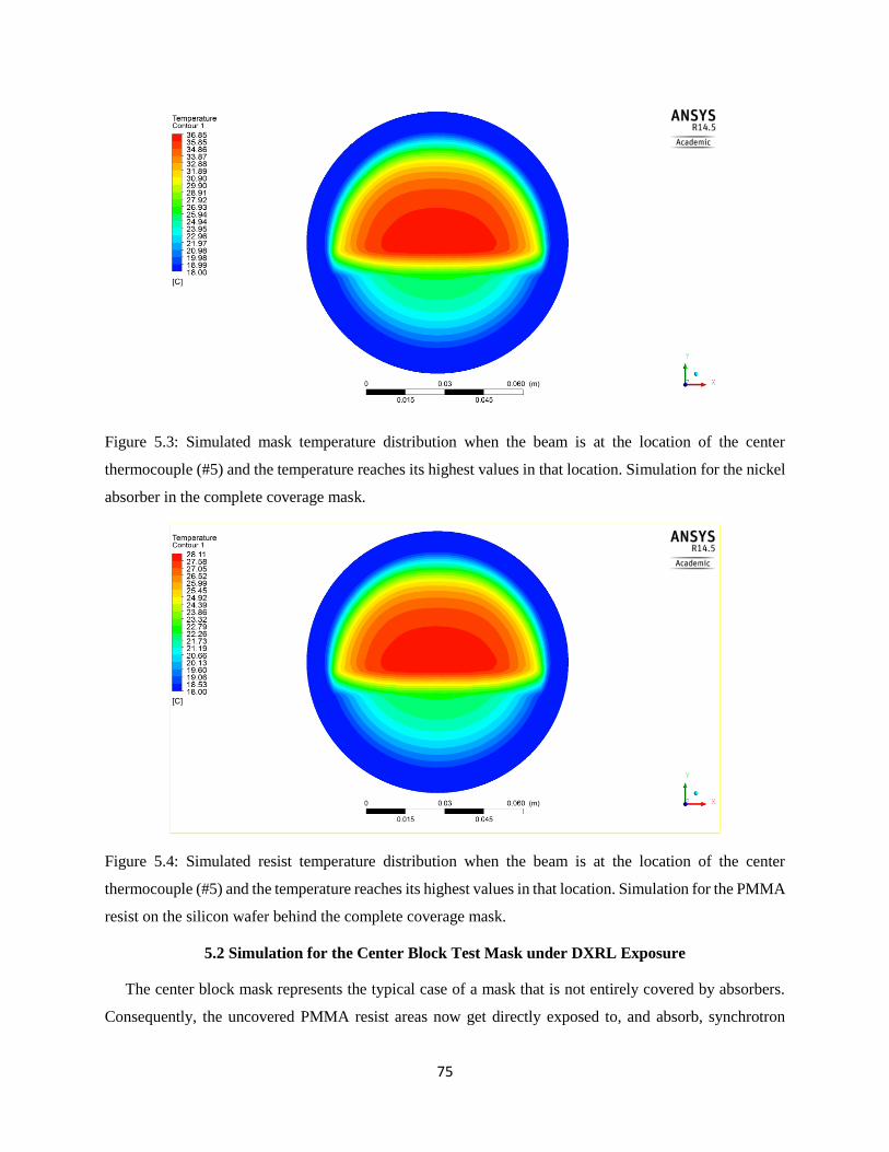
75
Figure 5.3: Simulated mask temperature distribution when the beam is at the location of the center
thermocouple (#5) and the temperature reaches its highest values in that location. Simulation for the nickel
absorber in the complete coverage mask.
Figure 5.4: Simulated resist temperature distribution when the beam is at the location of the center
thermocouple (#5) and the temperature reaches its highest values in that location. Simulation for the PMMA
resist on the silicon wafer behind the complete coverage mask.
5.2 Simulation for the Center Block Test Mask under DXRL Exposure
The center block mask represents the typical case of a mask that is not entirely covered by absorbers.
Consequently, the uncovered PMMA resist areas now get directly exposed to, and absorb, synchrotron

76
radiation. Two different standard resist thicknesses at SyLMAND are considered in this study: 250 μm and
500 μm. As explained in Chapter 1, different resist thicknesses require adjusted radiation spectra. To meet
the requirement of a specific top-to-bottom dose ratio, the double mirror system and pre-absorbers are
applied to change the spectrum of the synchrotron beam (see Table 5.2).
The beam powers absorbed in each layer, at 200 mA ring current, were recalculated with LEX-D to
serve as input data for the numerical simulation and is compiled in Figure 5.5. (see Appendix D) The 80
μm nickel absorber effectively absorbs almost the entire beam power, with infinitesimal energy transmitted
through it. In areas not covered by nickel absorbers, portions of the beam powers are deposited in the 30
μm polyimide membrane, in the 250 and 500 μm PMMA resist, and in the 500 μm silicon wafer (see
Appendix E). Absorption in the helium gas layer is negligible and was therefore not modeled, as well as
the infinitesimal energy deposited in unexposed PMMA and silicon wafer.
Figure 5.5: Beam power density distribution in the various layers of the extended DXRL exposure model
(input data obtained from LEX-D calculations, considering the 25% intensity chopper) for the center block
mask: Upper: 250 μm PMMA; Lower: 500 μm PMMA.

77
Table 5.2: Synchrotron beam parameters for DXRL exposures
PMMA
Thickness
(μm)
Mirror
Angle
(mrad)
Pre-absorber
Dose
Expenditure
(mA∙min)
Intensity
Chopper
open Duty
Cycle
Top-to-
Bottom Dose
Ratio
Incident Beam
Power (W) at
200 mA
calculated by
LEX-D
250 4 N/A 252 25% 14.46 : 3.5 14.31
500 N/A 150 μm
Kapton 424 25% 9.64 : 3.5 19.61
As the spectrum gets adjusted to be harder for the thicker PMMA layer, fewer hard spectral components
are cut in the beamline, and the overall incident beam power in the simulation model is consequently higher
than when exposing thinner PMMA layers (19.61 W as compared to 14.31 W). Mask absorbers are laid out
to always absorb close to all radiation impinging at any spectrum to be expected. With higher incident beam
power at thicker resist layers, more power will therefore get absorbed in the nickel absorbers (2.363 W/cm
as compared to 1.724 W/cm). The polyimide membrane, however, only absorbs a small fraction of the
incident beam power and gets even more transparent at higher photon energies. Due to a significantly lower
fraction of the beam power absorbed in the polyimide at harder spectra, less absolute power will get
absorbed in the polymer even at increased incident beam power (0.07 W/cm as compared to 0.218 W/cm).
The simulated temperature distributions in the center block mask and the 250 μm or 500 μm PMMA
resist layers are presented in Figure 5.6 to Figure 5.9.
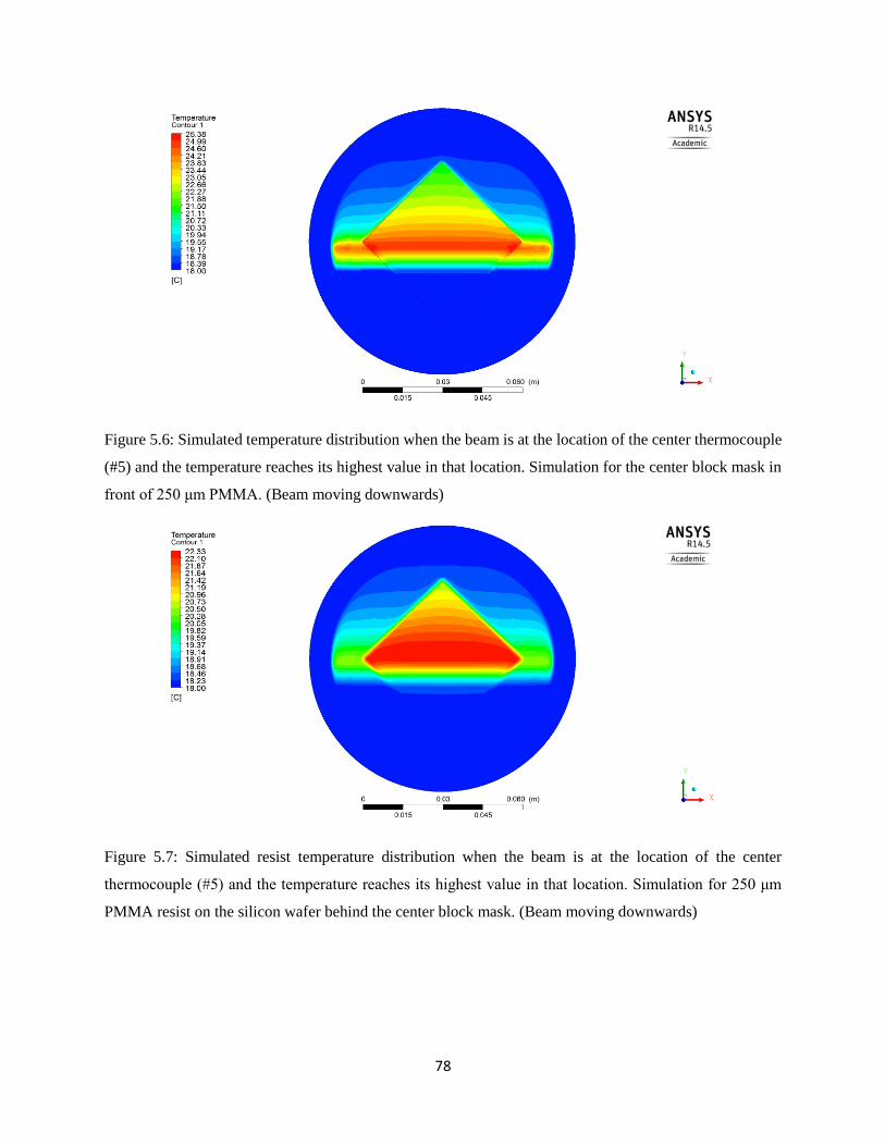
78
Figure 5.6: Simulated temperature distribution when the beam is at the location of the center thermocouple
(#5) and the temperature reaches its highest value in that location. Simulation for the center block mask in
front of 250 μm PMMA. (Beam moving downwards)
Figure 5.7: Simulated resist temperature distribution when the beam is at the location of the center
thermocouple (#5) and the temperature reaches its highest value in that location. Simulation for 250 μm
PMMA resist on the silicon wafer behind the center block mask. (Beam moving downwards)

79
Figure 5.8: Simulated temperature distribution when the beam is at the location of the center thermocouple
(#5) and the temperature reaches its highest value in that location. Simulation for the center block mask in
front of 500 μm PMMA. (Beam moving upwards)
Figure 5.9: Simulated resist temperature distribution when the beam is at the location of the center
thermocouple (#5) and the temperature reaches its highest value in that location. Simulation for 500 μm
PMMA resist on the silicon wafer behind the center block mask. (Beam moving upwards)
5.3 Thermoelastic Simulation for the Center Block Mask and PMMA Resist
Temperature distributions obtained from thermal simulations described above are now used in
thermoelastic simulations to quantify the thermal deformations occurring during DXRL exposures. The

80
center block mask and the PMMA resist as well as the silicon wafer are considered. The simulation for the
mask uses the same FEM model described in Chapter 3, as no changes occur to the mask deformation
mechanism in this case. The input temperatures, of course, are different now in the extended model. The
new aspect of the deformation model is that now the PMMA layer on the silicon wafer is modeled as well.
ANSYS Mechanical® is used, with the assumption of no slip or twist on the interface of the two components.
The silicon wafer is considered to be bonded solidly to the substrate holder without any relative movement
(see Figure 5.10). The mesh consists of 3.54·104 nodes and 6.37·103 elements. The mechanical properties
of PMMA and silicon are presented in Table 5.3.
Table 5.3: Mechanical properties of PMMA and silicon [10][78]
Material Thickness
(μm)
Coefficient of Thermal
Expansion
(K-1)
Young’s
Modulus
(GPa)
Poisson’s
Ratio
PMMA 250; 500 68·10-6 3.24 0.37
Silicon 500 2.6·10-6 169 0.28
Figure 5.10: Schematic of the PMMA-wafer assembly model

81
5.3.1 Exposure of 250 μm PMMA
The simulated deformations for the center block mask and 250 μm PMMA are presented in Figure 5.11
and Figure 5.12.
Figure 5.11: Simulated deformations (in micrometers) for the center block mask in front of 250 μm PMMA:
Upper Left: Total deformation; Upper Right: Deformation along the x-axis in the mask plane; Lower Left:
Deformation along the y-axis in the mask plane; Lower Right: Deformation along the z-axis opposing the
beam direction.

82
Figure 5.12: Simulated deformations (in micrometers) for the 250 μm thick PMMA layer behind the center
block mask: Upper Left: Total deformation; Upper Right: Deformation along the x-axis in the mask plane;
Lower Left: Deformation along the y-axis in the mask plane; Lower Right: Deformation along the z-axis
opposing the beam direction.

83
5.3.2 Exposure of 500 μm PMMA
The simulated deformations for the center block mask and 500 μm PMMA are presented in Figure 5.13
and Figure 5.14.
Figure 5.13: Simulated deformations (in micrometers) for the center block mask in front of 500 μm PMMA:
Upper Left: Total deformation; Upper Right: Deformation along the x-axis in the mask plane; Lower Left:
Deformation along the y-axis in the mask plane; Lower Right: Deformation along the z-axis opposing the
beam direction.

84
Figure 5.14: Simulated deformations (in micrometers) for the 500 μm thick PMMA layer behind the center
block mask: Upper Left: Total deformation; Upper Right: Deformation along the x-axis in the mask plane;
Lower Left: Deformation along the y-axis in the mask plane; Lower Right: Deformation along the z-axis
opposing the beam direction.

85
5.3.3 Summary of Simulation Results
The results of the thermoelastic simulations for DXRL exposures are presented in Table 5.4.
Table 5.4: Results of the thermoelastic simulations for DXRL exposures
Cases
Max
Temperature
(°C)
Max Total
Deformation
(μm)
Max X-axis
Deformation
(μm)
Max Y-axis
Deformation
(μm)
Max Z-axis
Deformation
(μm)
250 μm
PMMA
Mask 25.38 24.5 2.2 2.3 24.4
Resist 22.33 0.10 0.01 0.01 0.10
500 μm
PMMA
Mask 30.96 34.3 4.1 3.4 34.3
Resist 25.81 0.32 0.06 0.08 0.32
5.4 Discussion
The thermal simulations show that the reduced proximity gap leads to a net increase of the cooling
effectiveness despite the added PMMA-wafer assembly. The temperature rise in the complete coverage
mask is slightly reduced, by approximately 2°C, when compared to the previous thermal simulation from
Chapter 3 (compare Figure 3.10 and Figure 5.3). The mask now is heated up to 37°C. As before in Chapter
3, the heat gets dissipated along the mask absorbers to the mask frame, and across the proximity gap. This
latter contribution is more efficient now as the gap is much reduced. From the PMMA resist surface, the
heat is conducted, with limited efficiency compared to other solids, but better efficiency than across the
helium gas gap, to the cooled wafer (see Figure 5.3). The heat transfer through the PMMA resist heats it up
by 10°C even though the PMMA absorbed infinitesimal radiation behind the complete absorbers (see Figure
5.4).
For the center block mask, more UDFs were implemented in the model to obtain a better prediction of
the effects during DXRL exposure. Lower layers in the areas unprotected by absorbers get exposed: parts
of the polyimide membrane, of the PMMA, and of the silicon wafer also absorb beam power. Furthermore,
the entire model, whether behind absorbers or not, gets heated and cooled by conduction. The highest
temperatures occur in the center block mask. The resist underneath shows a similar lateral pattern of
temperature distribution as the mask, but at an infinitesimal level. It is therefore apparent that the dominant
heating mechanism of the resist is not direct absorption of radiation in PMMA behind transparent mask
areas, but conduction of heat absorbed in the mask absorbers just above the non-exposed PMMA areas. A
sharp temperature gradient in the PMMA layer is observed at the projected lateral layout boundaries of the
absorber (see Figure 5.7 and Figure 5.9). This is because PMMA has a low thermal conductivity (similar

86
to polyimide), and the lateral heat dissipation within the wide resist layer is much slower than it is in the
short axial direction towards the cooled silicon wafer. On the other hand, the exposed resist absorbs only
relatively small fractions of the locally beam power, leading to very limited radiation-induced energy
deposition in the resist layer. The observed, relatively low temperature rises in PMMA are critical to avoid
foaming and cracking [14]. The two incident beam powers of the realistic scenarios discussed in this chapter
(approximately 14-20W) exceed most of those values of the beam power studied by temperature
measurements in Chapter 4 (approximately 6-30 W). Yet, the temperature rises in the mask remain well
manageable.
The thermoelastic simulations show that during the DXRL exposure, the deformation in the PMMA
resist is at a much smaller scale (up to about 1%) compared to deformations in the center block mask (see
Table 5.4). Thus, the accuracy of pattern transfer is dominated by thermal deformations of the mask rather
than the resist. The deformations in the lateral plane (x-y plane), as integrated distortions across the entire
center block mask, amount to about 2 μm in each direction for 250 μm thick resist and about 4 μm in each
direction for 500 μm thick resist. This increase in the thicker resist reflects the increased temperatures due
to higher incident beam powers and reduced conduction through the thicker, poorly conducting PMMA.
As the local structure inaccuracy, deformations of several micrometers would be detrimental for most
MEMS applications. As an effect integrated over almost the entire wafer (few MEMS components are 6 cm
large and almost none have as large feature size as the center block mask), however, such results would
still be acceptable for most cases, and mostly translate into position inaccuracies. Yet, the results show the
outstanding importance of controlling the incident beam power to achieve a sufficient accuracy of pattern
transfer. The deformation of the absorber must always be kept at the lowest level possible. Thus, the
intensity chopper is a critical SyLMAND beamline component when implementing polyimide membrane
masks. When changing from 25% open duty cycle used in these simulations to 10%, temperature rises and
deformations would get reduced by a factor of 2.5, resulting in micron- or submicron deformations for the
most part. Further reductions could be achieved when the intensity chopper gets upgraded for continuous
duty cycle adjustability, and beam powers less than 10% can be selected. For complex patterns in a real X-
ray mask, the small feature size will also decrease the local temperature rise and deformation, which thermal
deformations might no longer be a dominant source of inaccuracy.
5.5 Chapter Summary
In this chapter, the simulation model from previous study was extended to study the thermal and
thermoelastic situation for DXRL exposures under realistic conditions: The extended model included 100 to
500 μm thick PMMA resist on a 500 μm thick silicon wafer, as well as reduced proximity gap of 100 μm.
This reduced proximity gap leads to a net increase of the cooling effectiveness despite the added PMMA-
87
wafer assembly. The temperature rise in the complete coverage mask is slightly reduced to only 37°C, when
compared to the previous thermal simulation from Chapter 3. The heat transfer through the mask-covered
PMMA resist heats it up by 10°C even though the PMMA does not itself absorb any radiation. For the
center block mask, resist underneath absorbers shows a similar lateral pattern of temperature distribution
as the mask, but at a lower level. Apparently, the dominant heating mechanism of the resist is conduction
of heat absorbed in the mask absorbers just above the non-exposed PMMA areas. A sharp temperature
gradient in the PMMA layer is observed at the projected lateral layout boundaries of the absorber. This is
because PMMA has a low thermal conductivity, and the lateral heat dissipation within the wide resist layer
is much slower than it is in the short axial direction towards the cooled silicon wafer. On the other hand,
the exposed resist absorbs only relatively small fractions of the local beam power, leading to very limited
radiation-induced energy deposition in the resist layer. The deformation in the PMMA resist is about 1%
of the deformations in the center block mask, and the accuracy of pattern transfer is dominated by thermal
deformations of the mask rather than the resist. In the lateral plane, integrated distortions across the entire
center block mask amount to about 2 μm in each direction for 250 μm thick resist and about 4 μm in each
direction for 500 μm thick resist. Local deformations are much smaller. The results still demonstrate the
significant importance of controlling the incident beam power, e.g. by means of the intensity chopper, to
achieve a sufficient accuracy of pattern transfer.

88
CHAPTER 6
SUMMARY AND CONCLUSION
6.1 Summary and Conclusion
This thesis aimed to identify and develop a viable fabrication approach for polyimide membrane X-ray
masks to be used at SyLMAND. Special consideration was given to quantify the anticipated heat load and
the resulting thermal deformations during exposure. The fabrication method for the polyimide membrane
X-ray mask was developed within the restrictions of materials (e.g. mask absorber plating alternatives) and
equipment (e.g. maximum achievable curing temperatures) available at SyLMAND. The heat load under
different beam power scenarios was analyzed numerically and verified experimentally. Subsequently, a
detailed study based on the simulated temperature distribution predicted the thermal deformations of test
masks for realistic deep X-ray lithography (DXRL) exposure scenarios with PMMA resist layers of
different thicknesses (250 μm; 500 μm) and silicon wafer substrates.
Two polyimide products, Evonik P84® and Durimide 7520® have been investigated as potential mask
membrane materials. Spin-coating experiments proved Durimide 7520® to generate a more homogeneous
membrane than P84® even after modifications for improved spin coating behaviour. A complete fabrication
sequence was developed for Durimide 7520 membranes, including patterning of mask absorber templates
in 100 μm thick negative tone UV resist NR26-25000P®, electroplating of the absorber structures in 80 μm
thick nickel, and release of the polyimide membrane through etching of the exposure window into the
stainless steel sacrificial substrate using FeCl3. The final polyimide X-ray test masks have 30 μm thick
polyimide membranes and 80 μm thick nickel absorbers, with an exposure window of 83-mm-diameter.
Two test masks were prepared, one with complete coverage of absorber, the other with a square absorber
layout at the center.
Thermal challenges often encountered when using polymer-based mask membranes can be controlled
using some of the SyLMAND laboratory’s design features: The intensity chopper at SyLMAND can
significantly reduce the heat load by changing the duty cycle of the incident synchrotron beam from 100%
to 10% or 25% of the full beam power. Also, the double mirror system and X-ray pre-absorbers can reduce
the beam power by modifying the beam spectrum. These instruments at SyLMAND allow quasi-continuous
beam power tuning, and therefore control of the heat load in the mask during exposure. Their impact on the
lithographic results was further studied:
Numerical simulations were carried out to analyze the temperature rise and resulting thermal
deformations: ANSYS FLUENT® was used for the thermal analysis by computational fluid dynamics, and
ANSYS Mechanical® was applied for thermoelastic analysis with the finite element method. The numerical

89
model was experimentally verified, using five thermocouples attached to the surface of the mask absorbers.
Temperature distributions in the test mask during exposure were obtained and verified the numerical model
of thermal simulation. However, some discrepancies on the order of 5°C existed between simulated and
measured temperatures. The error is caused by an unintentional tilt of the substrate holder during the
experiments, which locally changed the distance of the proximity gap.
It could be shown that the mechanism of heat dissipation between the mask as the primary absorber of
the incident beam power and the cooled surroundings of the mask is mainly through thermal conduction
across the proximity gap. The temperature of the X-ray mask increases proportionally with the incident
synchrotron beam power at otherwise constant conditions. Beam power tuning using the intensity chopper
and other beamline and storage ring properties can therefore be applied to control the temperature rise in
the polyimide X-ray mask. Temperatures obtained from numerical simulations and experimental results
were related to specific incident beam power values obtained from analytical results of photon-solid matter
interaction. Individual beam power – mask temperature values were finally interpolated to obtain a
generalized prediction of anticipated mask temperatures for different exposure scenarios. Typical final
temperatures amount to 30 to 40°C for incident beam power values around 10 W.
The polyimide membrane has a low thermal conductivity (0.12 W/m/K) and a high thermal expansion
coefficient (55·10-6 K-1), which can cause undesired thermal deformations of the locally exposed, and
heated, absorber patterns. The thermoelastic simulation results of DXRL exposure show that the
deformations in the lateral plane are only about 10% of the axial deformations. Only those lateral distortions
have a direct impact on the final structure accuracy of the lithographic process. For the center block mask,
the deformations in the lateral plane amount to approximately 2.3 μm for 250 μm thick PMMA, and to
approximately 4 μm for 500 μm thick PMMA. These deformations, integrated across the entire layout area,
are seen to not affect the accuracy of pattern transfer significantly, provided that the incident beam power
is reduced by the intensity chopper as was done in the studied cases. While the mask absorbers deformed
on the order of micrometers, the thermal deformations in the PMMA resist itself is limited to dozens of
nanometers, which can be neglected when compared to other sources of inaccuracies.
The results of the fabrication process and the thermal analyses promise successful application of
polyimide-based X-ray masks at SyLMAND. Thermal deformations of the absorber patterns can be
controlled to an acceptable level, so that thermoelastic deformations of the mask will not significantly
reduce the pattern transfer accuracy in the resist during exposure. The key component at SyLMAND to
achieve this goal is the intensity chopper which can effectively reduce the heat load in the polyimide X-ray
mask during exposure, at the cost of increased exposure times.

90
6.2 Future Work
The following items could be considered to expand the current research and to more thoroughly
investigate the topic:
As gold electroplating capabilities have now been developed at SyLMAND, future polyimide
masks can use gold absorbers so that thinner (and more easily fabricated) absorbers can be applied.
As a high resolution, direct-write UV laser lithography system is currently getting commissioned
at SyLMAND, high resolution mask templates can be fabricated on future polyimide X-ray masks.
The two points above allow to complete the fabrication sequence developed in this research with
improved absorber patterning techniques to fabricate XRL masks with complex MEMS layouts for further
studies and applications.
The experimental verification and analysis aspect could be further improved by replacing the
sensing approach: the simple thermocouples used to measure the temperature distribution in the X-
ray mask during exposure can be replaced by a costlier, but advanced infrared camera. The
development of thermographic technology now provides high resolution in both image and
temperature. For example, JENOPTIK produces an infrared camera with image resolution of 2014
× 1536 infrared pixels and thermal resolution of less than 0.05 Kelvin. The measurement with
advanced infrared camera can meet the requirements of real-time and high resolution, which is
much more detailed than using thermocouples. For this approach, however, such a camera would
have to be purchased. Furthermore, the viewport glass in the X-ray scanner would have to be
replaced with an infra-red-transparent alternative, or a vacuum feedthrough would have to be
designed and implemented.
The deformation of the mask layout incurred during the entire fabrication process needs to be
studied as a further cause of overall lithographic inaccuracies, beyond thermal deformations during
exposure. One such contribution to be studied would be the curvature of the mask under the impact
of the various thin films deposited. Measurements require a surface profiler. However, the
accessibility of a device that can measure the 4” substrate is limited at SyLMAND and the CLS. A
new optical profiler is currently getting procured and will be available soon, which will allow the
measurement of the mask curvature during the fabrication process.

91
APPENDIX A
TECHNICAL INFORMATION FOR POLYIMIDE MATERIALS
A.1 Polyimide Solution P84®
Table A.1: Mechanical properties of P84® compiled from vendor information (Evonik, Germany)
Tensile Strength (MPa) 140
Young’s Modulus (GPa) 3.9
Glass Transition Temperature (°C) 315
Thermal Decomposition Temperature (°C) 550
Coefficient of Thermal Expansion (10-6/°C) 50
Table A.2: Mixture of P84® and NEP
Evonik P84® Solution N-Ethyl-2-Pyrrolidone (NEP)
Density (g/cm3) 1.125 0.99
Volumetric Percent 70.00% 30.00%
Mixture Density (g/cm3) 1.129
Weight Percent 17.06% 82.94%
A.2 Photoresist Durimide 7520®
All information is compiled from vendor information (Fujifilm Electronic Materials U.S.A., Inc.;
North Kingstown, RI).[68]
Table A.3: Mechanical properties of Durimide 7520® [68]
Tensile Strength (MPa) 215
Young’s Modulus (GPa) 2.5
Glass Transition Temperature (°C) 285
Thermal Decomposition Temperature (°C) 525
Coefficient of Thermal Expansion (10-6/°C) 55

92
Table A.4: Processing parameters of Durimide 7520® [68]
Exposure Range 60-200 mJ/cm2
Soft Bake 100°C/3 min
Post Exposure Delay 20-22°C/30 min
Cure 350°C/60 min
Shrinkage from Soft Bake to Cure 45%
Figure A.1: Relationship between spin speed and cured film thickness for Durimide 7520®. [68]

93
APPENDIX B
SURFACE ROUGHNESS MEASUREMENTS FOR POLYIMIDE MASK FABRICATION
The surface roughness of the stainless steel substrate, of the polyimide membrane, and of the titanium layer
was measured using a Micromap 570 3D optical surface profiler manufactured by Micromap Corporation
(Tucson, AZ). The measuring window of the surface profiler is 1.254 mm × 0.934 mm. The measurement
mode was ‘wave mode’, which utilizes white light interferometry phase scans. The surface roughness of
the substrate and polyimide membrane was measured at the center of the sample. For the measurement of
the titanium layer, the surface roughness was measured at the center and two radii, 25 mm and 45mm (see
Figure B.1). For either radius, two different points were measured with the sample rotated by 90°. The
results of the surface roughness measurement are presented in Table B.1. The roughness values are given
based on two-dimensional area scans rather than conventional one-dimensional line scans. Associated
roughness values, according to new standards, include the area-average roughness Sa, given in units of
Ångström (10-10 m, or 10-4 μm).
Figure B.1: Positions of surface roughness measurements for the titanium layer.

94
Table B.1: Measured surface roughness at selected mask fabrication steps
Surface Average Roughness, Sa
(Å)
Maximum Height Difference, St
(Å)
Stainless Steel Substrate 1590 22960
Polyimide Membrane 596.9 15620
Titanium Layer @ Center 1693 22750
Titanium Layer @ R=25 mm 1346 18560
Titanium Layer @ R=25 mm - 90° 1598 23550
Titanium Layer @ R=45 mm 1622 25880
Titanium Layer @ R=45 mm - 90° 975.5 16760
Average of Titanium Layer 1447 21500

95
The original data for the seven measurement points mentioned above are present below.

96

97

98

99

100

101

102
APPENDIX C
CALCULATIONS OF 100 MBAR HELIUM GAS PROPERTIES AND DIMENSIONLESS NUMBERS
The equations to calculate relevant conditions associated with the 100 mbar helium buffering gas
atmosphere in the scanner working chamber are derived from [79]. The modelling parameters used in the
calculations are presented in Table C.1.
Table C.1: Modelling parameters for helium gas calculations
Ambient
pressure of
helium gas, P
Ambient
temperature of
helium gas, T∞
Specific heat
capacity of
helium gas, cp
Distance of
the proximity
gap, d
Relative
velocity of
helium gas, V
Reference
temperature, T0
100 mbar 291.15 K/18°C 5193 J/kg/K 1.4 mm 50 mm/s 273.15 K
C.1 Calculation of the Knudsen Number Kn of 100 mbar Helium at 18°C:
The Knudsen number is a dimensionless number used to judge the validation of the continuum
assumption. The characteristics of individual molecules/atoms are ignored, but the macroscopic effect of
the gas molecules/atoms is studied in the continuum model. The molecular-mean-free path (λ) is compared
to the characteristic dimension of the system, which is the proximity gap distance in this case: If this ratio
is low, the number of helium atoms within the control volume is large enough to be statistically meaningful,
and continuum fluid behavior can be assumed [80].
In the ideal gas law PV=NRT, N represents the amount of substance, R is the gas constant R= 8.314∙10-5
m3∙bar/K∙mol, and the Avogadro constant is N0= 6.023∙1023 mol-1. With the atomic diameter (σ) for
helium of σ = 3.74∙10-10 m, the gas law can be expressed as
23
6
2
3
0 2.488 10
16.468 10 m 6.468μm
2
4.620 10n
N
V
Kd
PNN
V RT
- Mean free path of 100 mbar helium gas at 18°C
Since the Knudsen number is within the interval of 0 to 0.1, continuum fluid mechanics with a slip flow
condition should be applied, where a relative velocity exists between the fluid and channel surface [81].

103
C.2 Calculation of the 100 mbar Helium Density ρ at 18°C:
1
3 3 3
1.20.17623 1 0.53 10 kg/m 0.016 kg/m
( ) ( )52
0 0
P P
T / T T / T
C.3 Calculation of the Dynamic Viscosity μ and Kinematic Viscosity ν of 100 mbar Helium at 18°C:
5 0.7 5
3 2
1.951.88 0
1.180
5 10 ( ) kg/m/s 10 kg/m/s
10 m /s
0T / T
C.4 Calculation of the Thermal Conductivity k of 100 mbar Helium Gas at 18°C:
44 0.71(1 2 10 )0.144(1 2.7 10 )( ) W/m/K W/m/K0.1507P
0k P T / T
C.5 Calculation of the Prandtl Number Pr and the Thermal Diffusivity α of 100 mbar Helium at
18°C:
The Prandtl number is a dimensionless number, defined as the ratio of momentum diffusivity with
respect to thermal diffusivity. For most gases, the Prandtl number is around 0.7. The thermal diffusivity
can be expressed in terms of the Prandtl number Pr and the kinematic viscosity ν:
3 2
0.6724
1.755 10 m /s
p
P
Pr
r
ck
C.6 Calculation of the Reynolds Number ReD and the Rayleigh Number RaD of 100 mbar Helium at
18°C:
The Reynolds number is a dimensionless number to judge the domain of fluid flow. If the flow is
characterized by random fluctuations in velocity, temperature, pressure, and density, it is referred to as
turbulent. In the absence of such fluctuations the flow is laminar.
For a fluid moving between two plane parallel surfaces, where the width of the surfaces is much greater
than the separation of the plates, the characteristic dimension is twice the separation of the plates [82]. The
Reynolds number of the 100 mbar Helium gas flow in the proximity gap therefore is based on the
characteristic dimension of twice the distance of the proximity gap, which is D = 2d = 2.8 mm.
0.1186D
VDRe

104
The critical Reynolds number for a fluid moving between plane parallel surfaces depends on
environmental conditions, but is on the order of 105 to 106. At smaller Reynolds numbers, the flow is laminar,
and turbulent at Reynolds numbers exceeding the critical Reynolds number. For the rarefied helium gas in
this study, with a very small Reynolds number of about 0.1, the domain of the flow is laminar.
Assuming that the maximum temperature in the mask surface is Ts=50°C=323.15 K, the temperature
difference to the scanner cooled to 18°C becomes ΔT=32 K. The film temperature Tf= (Tf +T∞)/2=
(50+18) °C/2=39°C=307.15 K.
Volumetric thermal expansion coefficient for ideal gas: 2
33.21 1 1
5 0( ) 6 1p
f
p
T RT T
The Rayleigh number indicates the relative importance of buoyancy forces to viscous dissipation and
diffusion forces. At low Rayleigh number, heat transfer is primarily through conduction, rather than natural
convection.
321.083 10D
gD TRa
At such low Rayleigh numbers, the fluid remains stagnant, and heat transfers through the proximity gap
by conduction [80].
C.7 Determination of the Time Step τ for Transient Thermal Simulation:
0.052sec 0.013sec 13msec4
Dt
gD T
[83]
C.8 Determination of the Heat Transfer Coefficient h of the Polyimide Membrane:
The polyimide membrane is exposed to the helium gas in the exposure window, where heat in the mask
can dissipate into the helium environment. To find the heat transfer coefficient h, the Rayleigh and Nusselt
numbers needed to be evaluated. The Nusselt number is a dimensionless heat transfer coefficient, which
describes the ratio of convective to conductive heat transfer across the boundary of the control volume.
With the length of the polyimide membrane surface (diameter of the exposure window): L=83 mm=0.083 m
and the Rayleigh number as explained above, but now calculated for the length L rather than the
characteristic dimension D of the proximity gap,

105
1
3
/41/4
2
235.1
2.0062.435 4.884 4.953
3.783W/m /K
L L1/ 2
Lcon
L
v
PrNu Ra
Pr + Pr
Nu k
T
h
La
L
gR
- Average Nusselt number of vertical plate

106
APPENDIX D
LEX-D CALCULATION FOR THE POWER ABSORPTION IN DIFFERENT MATERIAL LAYERS
The powers absorbed in the different layers of material are needed as input data for the thermal simulations.
The results are calculated by the software LEX-D (LIGA Exposure-Development) from Sandia National
Labs, Livermore, USA, which given by the difference between power input and output through the material
layer. The input and output power densities are obtained in terms of the unit power Watt with respect to
unit horizontal increment of 1 mrad with 17 m beam trajectory from bending magnet (e.g. 1.7 cm wide at
the exposed sample in horizontal direction) per mA beam current, as well as the unit power Watt at 200
mA beam current per cm horizontal increment at sample. The standard beam current assumed in the LEX-
D calculation is 200 mA. The obtained power densities can be proportionally adjusted to the exact electron
beam current for each simulation. The power absorption rates are calculated based on the uniform beam
width of 83 mm (8.3 cm). The results for absorbed power taking into account the intensity chopper with
25% open duty cycle (bold values in the table below) are used in the User Defined Functions (UDFs) for
ANSYS FLUENT® in the thesis. The absorbed powers in each material layer for different simulation cases
are presented in Table D.1.

Table D.1: LEX-D results for power absorption in different material layers
Simulation
Cases
Material
Layers
Power IN
[W/mrad/mA]
Power IN
[W/cm]
Power OUT
[W/mrad/mA]
Power OUT
[W/cm]
Power
Absorption
[W/cm] at
current of
Power
Absorption
[W/8.3cm] at
current of
Power
Absorption with
25% Chopper
[W/8.3 cm]
200 mA
Chapter 3
80 μm Nickel
0.0662 7.784
0.0069 0.814 6.970 57.85 14.46
30 μm
Polyimide 0.0653 7.684 0.100 0.830 0.207
Chapter 5:
250 μm
PMMA
80 μm Nickel
0.0585 6.921
0.0002 0.0235 6.898 57.25 14.31
30 μm
Polyimide 0.0511 6.048 0.873 7.246 1.811
250 μm
PMMA 0.0511 6.048 0.0323 3.817 2.231 18.52 4.629
500 μm
Silicon Wafer 0.0323 3.817 0.0009 0.106 3.711 30.80 7.700
Chapter 5:
500 μm
PMMA
80 μm Nickel
0.0870 10.29
0.0071 0.838 9.452 78.45 19.61
30 μm
Polyimide 0.0846 10.00 0.290 2.407 0.602
500 μm
PMMA 0.0846 10.00 0.0655 7.743 2.257 18.73 4.683
500 μm
Silicon Wafer 0.0655 7.743 0.0210 2.478 5.265 43.70 10.92
10
7

108
APPENDIX E
USER DEFINED FUNCTIONS (UDF) IN THE ANSYS FLUENT SIMULATION
E.1 UDF for the Thermal Simulation in Chapter 3:
#include "udf.h"
#define FLUXC 9.2892e10 /*to define the internal heat generation in the unit of W/μm/m2*/
static real ymin=-0.0044,ymax=0.0044,ym=0.0,vv=-0.05; /*to define the geometry, starting position, and
velocity of beam*/
static real tt1=0.0; /*to define the initial time*/
DEFINE_PROFILE(flux,tf,i) /* to define a custom boundary profile that varies as a function of spatial
coordinates and time.*/
{
face_t f; /*index that a wall face*/
real tt,xc[ND_ND],det; /*to define variable declarations, xc will hold the position
vector*/
tt=CURRENT_TIME; /*real current flow time (in seconds)*/
det=tt-tt1; /*to define time step*/
tt1=tt; /*renewed flow time*/
ymin=ymin+vv*det; /*displacement of the beam at each time step*/
ymax=ymax+vv*det;
ym=ym+vv*det;
if(ymin>=0.04775)vv=-0.05; /*to define scanning range of the beam and reciprocal
motion*/
if(ymax<=-0.04775)vv=0.05;
begin_f_loop(f,tf)
{
F_CENTROID(xc,f,tf); /*centroid is defined to specify position
dependent profiles*/

109
if(fabs(xc[1])<=0.0375&&sqrt(xc[0]*xc[0]+xc[1]*xc[1])<=0.0415&&xc
[1]<=ymax&&xc[1]>=ymin) /*to define the boundary of heat flux*/
{
F_PROFILE(f,tf,i) =FLUXC;
}
else
{
F_PROFILE(f,tf,i) =0.0;
}
}
end_f_loop(f,tf)
}
E.2 UDF for the DXRL Exposure Thermal Simulation in Chapter 5:
#include "udf.h"
#define FLUXC 0.6451e10
static real ymin=-0.0044,ymax=0.0044,ym=0.0,vv=-0.05;
static real tt1=0.0;
DEFINE_PROFILE(flux,tf,i)
{
face_t f;
real tt,xc[ND_ND],det;
tt=CURRENT_TIME;
det=tt-tt1;
tt1=tt;
ymin=ymin+vv*det;
ymax=ymax+vv*det;

110
ym=ym+vv*det;
if(ymin>=0.04775)vv=-0.05;
if(ymax<=-0.04775)vv=0.05;
begin_f_loop(f,tf)
{
F_CENTROID(xc,f,tf);
if(fabs(xc[1])<=0.0375&&sqrt(xc[0]*xc[0]+xc[1]*xc[1])<=0.0415&&xc
[1]<=ymax&&xc[1]>=ymin&&(fabs(xc[0])+fabs(xc[1]))>=0.03) /*to
define the boundary of heat flux on PMMA/wafer, considering the layout
of center block absorber*/
{
F_PROFILE(f,tf,i) =FLUXC;
}
else
{
F_PROFILE(f,tf,i) =0.0;
}
}
end_f_loop(f,tf)
}

111
APPENDIX F
TEMPERATURE MEASUREMENTS FOR THE TEST MASKS
F.1 Measurements for the Complete Coverage Test Mask
The measurement results for each test are presented below:
Test 1:
I = 218.5 mA, 10% chopper, with pre-absorbers; calculated incident beam power PLEX-D = 6.32 W
Test 2:
I = 235.5 mA, 10% chopper, without pre-absorbers; calculated incident beam power PLEX-D = 11.91 W

112
Test 3:
I = 178.2 mA, 10% chopper, with pre-absorbers; calculated incident beam power PLEX-D = 12.89 W
Test 4:
I = 202.6 mA, 10% chopper, with pre-absorbers; calculated incident beam power PLEX-D = 14.65 W

113
Test 5:
I = 219.6 mA, 10% chopper, with pre-absorbers; calculated incident beam power PLEX-D = 15.88 W
Test 6:
I = 233.2 mA, 10% chopper, with pre-absorbers; calculated incident beam power PLEX-D = 16.86 W

114
Test 7:
I = 222.3 mA, 10% chopper, without pre-absorbers; calculated incident beam power PLEX-D = 28.10 W
F.2 Measurements for the Center Block Test Mask
The measurement results for each test are presented below:
Test 1:
I = 214.3 mA, 10% chopper, with pre-absorbers; calculated incident beam power PLEX-D = 6.20 W

115
Test 2:
I = 210.6 mA, 10% chopper, without pre-absorbers; calculated incident beam power PLEX-D = 10.65 W
Test 3:
I = 182.6 mA, 25% chopper, with pre-absorbers; calculated incident beam power PLEX-D = 13.13 W

116
Test 4:
I = 188.8 mA, 25% chopper, with pre-absorbers; calculated incident beam power PLEX-D = 13.65 W
Test 5:
I = 206.2 mA, 25% chopper, with pre-absorbers; calculated incident beam power PLEX-D = 14.91 W

117
Test 6:
I = 238.4 mA, 25% chopper, with pre-absorbers; calculated incident beam power PLEX-D = 17.24 W
Test 7:
I = 207.7 mA, 25% chopper, without pre-absorbers; calculated incident beam power PLEX-D = 26.25 W

118
BIBLIOGRAPHY
[1] J. S. Greeneich, “X-ray lithography: Part I. Design criteria for optimizing resist energy absorption;
Part II. Pattern replication with polymer masks,” IEEE Trans. Electron Devices, vol. 22, no. 7, pp.
434–439, Jul. 1975.
[2] E. Spiller and R. Feder, “X-Ray Lithography,” in X-Ray Optics, vol. 22, H.-J. Queisser, Ed. Berlin,
Heidelberg: Springer Berlin Heidelberg, 1977.
[3] E. W. Becker, W. Ehrfeld, D. Münchmeyer, H. Betz, A. Heuberger, S. Pongratz, W. Glashauser,
H. J. Michel, and R. v. Siemens, “Production of separation-nozzle systems for uranium enrichment
by a combination of X-ray lithography and galvanoplastics,” Naturwissenschaften, vol. 69, no. 11,
pp. 520–523, Nov. 1982.
[4] E. Spiller, D. E. Eastman, R. Feder, W. D. Grobman, W. Gudat, and J. Topalian, “Application of
synchrotron radiation to x-ray lithography,” J. Appl. Phys., vol. 47, no. 12, pp. 5450–5459, 1976.
[5] U. Wallrabe, MEMS: A Practical Guide to Design, Analysis, and Applications. Berlin, Heidelberg:
Springer Berlin Heidelberg, 2006.
[6] E. W. Becker, W. Ehrfeld, P. Hagmann, A. Maner, and D. Münchmeyer, “Fabrication of
microstructures with high aspect ratios and great structural heights by synchrotron radiation
lithography, galvanoforming, and plastic moulding (LIGA process),” Microelectron. Eng., vol. 4,
no. 1, pp. 35–56, May 1986.
[7] T. Mappes, S. Achenbach, and J. Mohr, “X-ray lithography for devices with high aspect ratio
polymer submicron structures,” Microelectron. Eng., vol. 84, no. 5–8, pp. 1235–1239, May 2007.
[8] H. H. Gatzen, V. Saile, and J. Leuthold, Micro and Nano Fabrication. Berlin, Heidelberg:
Springer-Verlag Berlin Heidelberg, 2015.
[9] T. R. Christenson and H. Guckel, “X-Ray Lithography for Micromechanics,” Proceedings of
SPIE, vol. 2639, pp. 134–145, 2005.
[10] D. R. Hines, N. P. Siwak, L. A. Mosher, R. Ghodssi, M. Materials, and P. Handbook, MEMS
Materials and Processes Handbook, vol. 1. Boston, MA: Springer US, 2011.
[11] T. Christenson, “X-Ray Based Fabrication,” in MEMS: Design and Fabrication, M. Gad-el-Hak,
Ed. Boca Raton, FL: CRC Press, 2006, pp. 1–53.
[12] J. Mohr, W. Ehrfeld, and D. Münchmeyer, “Analyse der Defektursachen und der Genauigkeit der
Strukturübertragung bei der Röngentiefenlithographie mit Synchrotronstrahlung,”

119
Kernforschungszentrum Karlsruhe, vol. 4414, pp. 1–96, 1988.(in German)
[13] S. Achenbach, F. Pantenburg, and J. Mohr, “Optimierung der Prozeßbedingungen zur Herstellung
von Mikrostrukturen durch ultratiefe Röntgenlithographie (UDXRL),” 2000. (in German)
[14] V. Saile, LIGA and Its Applications. John Wiley & Sons, 2009.
[15] A. El-Kholi, P. Bley, J. Göttert, and J. Mohr, “Examination of the solubility and the molecular
weight distribution of PMMA in view of an optimised resist system in deep etch x-ray
lithography,” Microelectron. Eng., vol. 21, no. 1–4, pp. 271–274, Apr. 1993.
[16] V. Nazmov, E. Reznikova, J. Mohr, A. Snigirev, I. Snigireva, S. Achenbach, and V. Saile,
“Fabrication and preliminary testing of X-ray lenses in thick SU-8 resist layers,” Microsyst.
Technol., vol. 10, no. 10, pp. 716–721, 2004.
[17] F. J. Pantenburg, “Instrumentation for Microfabrication with Deep X-ray Lithography,” in AIP
Conference Proceedings, 2007, vol. 879, pp. 1456–1461.
[18] F. Pérennès and F. J. Pantenburg, “Adhesion improvement in the deep X-ray lithography process
using a central beam-stop,” Nucl. Instruments Methods Phys. Res. Sect. B Beam Interact. with
Mater. Atoms, vol. 174, pp. 317–323, 2001.
[19] F. J. Pantenburg and J. Mohr, “Influence of secondary effects on the structure quality in deep X-
ray lithography,” Nucl. Instruments Methods Phys. Res. Sect. B Beam Interact. with Mater. Atoms,
vol. 97, no. 94, pp. 551–556, 1995.
[20] B. Maid, “Anpassung der spektralen Verteilung der Synchrotronstrahlung für die
Röntgentiefenlithografie.” Kernforschungszentrum Karlsruhe, 1989. (in German)
[21] K. H. Gil, S. S. Lee, and Y. Youm, “Equations of exposure time and X-ray mask absorber
thickness in the LIGA process,” Microsyst. Technol., vol. 7, no. 1, pp. 1–5, Mar. 2001.
[22] B. L. Henke, E. M. Gullikson, and J. C. Davis, “X-Ray Interactions: Photoabsorption, Scattering,
Transmission, and Reflection at E = 50-30,000 eV, Z = 1-92,” At. Data Nucl. Data Tables, vol. 54,
no. 2, pp. 181–342, Jul. 1993.
[23] C. K. Malek, K. H. Jackson, W. D. Bonivert, and J. Hruby, “Masks for high aspect ratio x-ray
lithography,” J. Micromechanics Microengineering, vol. 6, no. 2, pp. 228–235, Jun. 1996.
[24] S. K. Griffiths and A. Ting, “The influence of X-ray fluorescence on LIGA sidewall tolerances,”
Microsyst. Technol., vol. 8, no. 2–3, pp. 120–128, 2002.
[25] W. Schomburg, P. Bley, H. Hein, and J. Mohr, “Masken für die Röntgentiefenlithographie,” VDI

120
Berichte, vol. 870, pp. 133–154, 1990. (in German)
[26] D. L. Laird, “Practical considerations in x-ray mask mounting methodology,” J. Vac. Sci. Technol.
B Microelectron. Nanom. Struct., vol. 11, no. 1993, p. 2953, 1993.
[27] D. Laird and R. Engelstad, “Predicting out-of-plane distortions during X-ray mask fabrication,”
Microelectron. Eng., vol. 30, no. 1–4, pp. 223–226, Jan. 1996.
[28] S. K. Griffiths, “Fundamental limitations of LIGA x-ray lithography: sidewall offset, slope and
minimum feature size,” J. Micromechanics Microengineering, vol. 14, no. 7, pp. 999–1011, Jul.
2004.
[29] L. Wang, Y. M. Desta, R. K. Fettig, J. Goettert, H. Hein, P. Jakobs, and J. Schulz, “High
resolution x-ray mask fabrication by a 100 keV electron-beam lithography system,” J.
Micromechanics Microengineering, vol. 14, no. 5, pp. 722–726, 2004.
[30] W. Dai and R. Nassar, “A three-dimensional numerical method for thermal analysis in X-ray
lithography,” Int. J. Numer. Methods Heat Fluid Flow, vol. 8, no. 4, pp. 409–423, Jun. 1998.
[31] A. Chiba and K. Okada, “Dynamic in-plane thermal distortion analysis of an x-ray mask
membrane for synchrotron radiation lithography,” J. Vac. Sci. Technol. B Microelectron. Nanom.
Struct., vol. 9, no. 6, p. 3275-3279, Nov. 1991.
[32] V. Nazmov, E. Reznikova, and J. Mohr, “Investigation of the radiation-induced thermal flexure of
an x-ray lithography mask during a tilted exposure,” J. Vac. Sci. Technol. B Microelectron.
Nanom. Struct., vol. 29, no. 1, p. 011007, 2011.
[33] S. Achenbach, F. J. Pantenburg, and J. Mohr, “Numerical simulation of thermal distortions in deep
and ultra deep X-ray lithography,” Microsyst. Technol., vol. 9, no. 3, pp. 220–224, Jan. 2003.
[34] K. Yamazaki, “Evaluation of temperature rise and thermal distortions of x-ray mask for
synchrotron radiation lithography,” J. Vac. Sci. Technol. B Microelectron. Nanom. Struct., vol. 12,
no. 6, p. 4028-4032, Nov. 1994.
[35] Y. Utsumi, T. Kishimoto, T. Hattori, and H. Hara, “Large area and wide dimensions X-ray
lithography using energy variable synchrotron radiation,” Microsyst. Technol., vol. 13, no. 5–6,
pp. 417–423, 2007.
[36] Y. Vladimirsky, J. Maldonado, R. Fair, R. Acosta, O. Vladimirsky, R. Viswanathan, H. Voelker,
F. Cerrina, G. M. Wells, M. Hansen, and R. Nachman, “Thermal effects in x-ray masks during
synchrotron storage ring irradiation,” J. Vac. Sci. Technol. B Microelectron. Nanom. Struct., vol.
7, no. 6. p. 1657, 1989.

121
[37] A. Ting, “Temperature rise of the silicon mask-PMMA resist assembly during LIGA exposure,”
Technical Report SAND2004-4446, Sandia National Laboratory, 2004.
[38] I. A. Shareef, J. R. Maldonado, Y. Vladimirsky, and D. L. Katcoff, “Thermoelastic behavior of X-
ray lithography masks during irradiation,” IBM J. Res. Dev., vol. 34, no. 5, pp. 718–735, Sep.
1990.
[39] D. J. Resnick, S. V. Pendharkar, W. J. Dauksher, K. D. Cummings, M. F. Laudon, B.
Romanowicz, P. Renaud, and R. L. Engelstad, “Thermal characteristics of an X-ray mask during
pattern transfer,” Microelectron. Eng., vol. 41–42, pp. 287–290, Mar. 1998.
[40] G. Feiertag, M. Schmidt, and A. Schmidt, “Thermoelastic deformations of masks for deep X-ray
lithography,” Microelectron. Eng., vol. 27, pp. 513–516, 1995.
[41] K. Marumoto, S. Aya, H. Yabe, T. Okada, and H. Sumitani, “Theoretical Analysis on Mechanical
Deformation of Membrane-Based Photomask Blanks,” Jpn. J. Appl. Phys., vol. 51, p. 46505, Apr.
2012.
[42] M. Karnezos, “Effects of stress on the stability of x-ray masks,” J. Vac. Sci. Technol. B
Microelectron. Nanom. Struct., vol. 4, no. 1986, p. 226-229, 1986.
[43] M. Laudon, A. H. Fisher, R. Engelstad, F. Cerrina, K. Cummings, W. Dauksher, D. Resnick, W.
Johnson, and D. Puisto, “Prediction of in-plane distortions due to mask fabrication processes,”
Microelectron. Eng., vol. 35, no. 1–4, pp. 549–552, Feb. 1997.
[44] M. S. De Jong, L. O. Dallin, and R. M. Silzer, “Canadian Light Source status,” J. Synchrotron
Radiat., vol. 11, no. 2, pp. 214–214, Mar. 2004.
[45] S. Achenbach, V. Subramanian, D. Klymyshyn, and G. Wells, “Synchrotron laboratory for micro
and nano devices: facility concept and design,” Microsyst. Technol., vol. 16, no. 8–9, pp. 1293–
1298, May 2010.
[46] V. Subramanian, S. Achenbach, D. Klymyshyn, G. Wells, W. Dolton, V. Nagarkal, B. Yates, C.
Mullin, and M. Augustin, “In situ diagnostic capabilities for beam position and beam intensity
monitoring at SyLMAND,” Microsyst. Technol., vol. 16, no. 8–9, pp. 1547–1551, May 2010.
[47] A. Chiba, M. Futagami, K. Okada, and T. Kato, “Effect of Helium Gas Pressure on X-Ray Mask
Heating during Synchrotron Radiation Exposure,” Jpn. J. Appl. Phys., vol. 34, no. Part 1, No. 1,
pp. 75–80, Jan. 1995.
[48] G. Aigeldinger, “Implementation of an Ultra Deep X-ray Lithography ( UDXRL ) System at
CAMD,” Universität Freiburg im Breisgau, 2001.

122
[49] Operating manual X-Ray Scanner DEX04. JENOPTIK Laser, Optik, Systeme GmbH, 2007.
[50] R. Lawes, “Manufacturing costs for microsystems/MEMS using high aspect ratio microfabrication
techniques,” Microsyst. Technol., vol. 13, no. 1, pp. 85–95, 2007.
[51] H.-G. Woo and H. Li, Advanced Functional Materials. Berlin, Heidelberg: Springer Berlin
Heidelberg, 2011.
[52] C.J.M. van Rijn, Ed., “Nano and Micro Engineered Membrane Technology,” in Membrane
Science and Technology, vol. 10, Elsevier, pp. 335–346, 2004.
[53] M. E. Grady, P. H. Geubelle, and N. R. Sottos, “Interfacial adhesion of photodefinable polyimide
films on passivated silicon,” Thin Solid Films, vol. 552, pp. 116–123, Feb. 2014.
[54] W. C. Wilson and G. M. Atkinson, “Review of Polyimides Used in the Manufacturing of Micro
Systems,” Technical Report, NASA/TM-2007-214870, 2007.
[55] K. Kurabayashi, M. Asheghi, M. Touzelbaev, and K. E. Goodson, “Measurement of the thermal
conductivity anisotropy in polyimide films,” J. Microelectromechanical Syst., vol. 8, no. 2, pp.
180–191, Jun. 1999.
[56] G. Strobl, The physics of polymers: Concepts for understanding their structures and behavior.
New York, NY: Springer Berlin Heidelberg, 2007.
[57] D.-J. Liaw, K.-L. Wang, Y.-C. Huang, K.-R. Lee, J.-Y. Lai, and C.-S. Ha, “Advanced polyimide
materials: Syntheses, physical properties and applications,” Prog. Polym. Sci., vol. 37, no. 7, pp.
907–974, Jul. 2012.
[58] L. M. Nicholson, K. S. Whitley, T. S. Gates, and J. A. Hinkley, “Influence of molecular weight on
the mechanical performance of a thermoplastic glassy polyimide,” J. Mater. Sci., vol. 35, no. 24,
pp. 6111–6121, 2000.
[59] H. Mitsui, R. Kumazawa, T. Tanii, T. Chugun, Y. Ohsawa, T. Ozaki, and K. Takayama,
“Synchrotron radiation damage test of insulating materials in the TRISTAN MR,” Proc. Int. Conf.
Part. Accel., vol. 52, pp. 31–44, 1993.
[60] F.-Y. Tsai, Y.-H. Kuo, and D. R. Harding, “Properties and structure of vapor-deposited polyimide
upon electron-beam irradiation,” J. Appl. Phys., vol. 99, no. 6, p. 64910, 2006.
[61] S. Achenbach, “Private communication.” .
[62] A. A. Harchenko, D. I. Brinkevich, S. D. Brinkevich, M. G. Lukashevich, and V. B. Odzhaev,
“Radiation-induced modification of polymer surfaces,” J. Surf. Investig. X-ray, Synchrotron

123
Neutron Tech., vol. 9, no. 2, pp. 371–376, 2015.
[63] D. C. Flanders and H. Smith, “Polyimide membrane x-ray lithography masks—Fabrication and
distortion measurements,” J. Vac. Sci. Technol., vol. 15, no. 3, p. 995, May 1978.
[64] T. Wada, S. Sakurai, and K. Kawabuchi, “Fabrication of polyimide x-ray masks with high
dimensional stability,” J. Vac. Sci. Technol., vol. 19, no. 4, p. 1208, 1981.
[65] S. Kinuta, Y. Saita, M. Kobayashi, M. Boerner, V. Saile, and S. Hosaka, “Polyimide-based X-ray
masks with advanced performance of pattern accuracy and thermal stability,” Microsyst. Technol.,
vol. 16, no. 8–9, pp. 1299–1302, May 2010.
[66] S. Achenbach, M. Boerner, S. Kinuta, W. Bacher, J. Mohr, V. Saile, and Y. Saotome, “Structure
quality in deep X-ray lithography applying commercial polyimide-based masks,” Microsyst.
Technol., vol. 13, no. 3–4, pp. 349–353, Jun. 2006.
[67] S. James and W. Alexander, Materials Science and Engineering Handbook, 3rd ed. Boca Raton,
FL: CRC Press, 2001.
[68] Fujifilm Electronic Materials, “Durimide 7500 Technical Information.” Fuji Films Electronic
Materials Inc., 2012.
[69] A. A. Taylor, M. J. Cordill, L. Bowles, J. Schalko, and G. Dehm, “An elevated temperature study
of a Ti adhesion layer on polyimide.,” Thin Solid Films, vol. 531, no. C, pp. 354–361, Mar. 2013.
[70] J. Kouba, Z.-G. Ling, L. Wang, Y. M. Desta, and J. Goettert, “Fabrication of large-area x-rays
masks for UDXRL on beryllium using thin film UV lithography and x-ray backside exposure,” in
Micromachining and Microfabrication Process Technology, vol. 5342, pp. 173–181, 2004.
[71] G. E. A. D. I. B. Ari and J. A. Di Bari, “Electrodeposition of nickel,” in Modern Electroplating,
5th ed., Hoboken, N.J.: John Wiley and Sons, pp. 79–114, 2011.
[72] D. M. Allen and H. J. a Almond, “Characterisation of aqueous ferric chloride etchants used in
industrial photochemical machining,” J. Mater. Process. Technol., vol. 149, no. 1–3, pp. 238–245,
2004.
[73] J. H. Lienhard IV and J. H. Lienhard V, A Heat Transfer Textbook, 4th ed. Cambridge, MA:
Phlogiston Press, 2011.
[74] J. R. Howell, M. P. Menguc, and R. Siegel, Thermal Radiation Heat Transfer, 5th ed. Boca Raton,
FL: CRC Press, 2010.
[75] A. Chiba, M. Futagami, and K. Okada, “Wafer Temperature Measurement and X-Ray Mask

124
Temperature Evaluation in Synchrotron Radiation Lithography,” Jpn. J. Appl. Phys., vol. 32, no.
Part 1, No. 2, pp. 753–757, Feb. 1993.
[76] M. R. Eslami, Finite Elements Methods in Mechanics, vol. 216, no. 4. Springer International
Publishing Switzerland, 2014.
[77] M. R. Eslami, R. B. Hetnarski, J. Ignaczak, N. Noda, N. Sumi, and Y. Tanigawa, Theory of
Elasticity and Thermal Stresses, vol. 197. Dordrecht: Springer Netherlands, 2013.
[78] M. A. Hopcroft, W. D. Nix, and T. W. Kenny, “What is the Young’s Modulus of Silicon?,” J.
Microelectromechanical Syst., vol. 19, no. 2, pp. 229–238, Apr. 2010.
[79] H. Petersen, “The properties of helium: density, specific heats, viscosity, and thermal conductivity
at pressures from 1 to 100 bar and from room temperature to about 1800 K,” Danish Atomic
Energy Commission, RPRT, 1970.
[80] L. M. Jiji, Heat Convection. New York, NY: Springer-Verlag Berlin Heidelberg, 2006.
[81] R. Barber and D. Emerson, “A numerical investigation of low Reynolds number gaseous slip flow
at the entrance of circular and parallel plate micro-channels,” in Proc. ECCOMAS Computational
Fluid Dynamics Conference, Swansea, UK, September 4-7, 2001.
[82] R. W. Fox, P. J. Pritchard, and A. T. Mcdonald, Introduction to fluid mechanics, 6th ed. Hoboken,
NJ: Wiley, 2004.
[83] ANSYS Inc., “ANSYS FLUENT theory guide,” ANSYS Inc., Canonsburg, PA, 2013.