fabrication of surface plasmon biosensors in cytop
TRANSCRIPT
Fabrication of Surface Plasmon Biosensors in CYTOP
By Hamoudi Asiri
A thesis submitted to the faculty of Graduate and Post-Doctoral Studies in partial fulfilment of the requirements for the degree of Masters of Applied Science in Chemical Engineering.
13/09/2012
Department of Chemical and Biological Engineering University of Ottawa
Ottawa, Ontario, Canada
© Hamoudi Asiri, Ottawa, Canada, 2012

I
ACKNOWLEDGEMNETS
I would like to thank my parents and brother first and foremost for their support
and guidance throughout the years and for their patience while I completed my studies. I
would also like to thank all the contributors to my research, particularly my thesis
supervisors, Dr. Pierre Berini and Dr. Niall Tait, for their direction and for giving me the
opportunity to complete the works described herein. Furthermore, I would like to thank the
technical support staff at the University of Ottawa, Ewa Lisicka and Michal Tensor, for their
assistance and expertise in materials processing and device testing. I would like to thank my
predecessors and colleagues, Charles Chiu, Raza Haniff, Norman Fong, Alex Krupin and Asad
Khan for their hard work and assistance with my assimilation into the project. Finally I
would like to thank the Carleton University Micro-fabrication lab personnel, Rob Vandusen,
Rick Adams and Angela Burns for their assistance in fabrication techniques and equipment
usage as well as providing me with the necessary training to carry out my research.

II
ABSTRACT
This thesis describes work carried out on the research, development and
implementation of new processes for the fabrication of surface plasmon waveguide
biosensors. Fabrication of surface plasmon resonance (SPR) based waveguides embedded in
a thick CYTOP cladding with the incorporation of fluidic channels was achieved with
improved quality and operability compared to previous attempts. The fabrication flow was
modified in key areas including lithography for feature definition, gold evaporation and the
upper cladding deposition procedure. The combined result yielded devices with sharper
resolution of waveguides, gold surfaces with minimal aberrations, reduced surface
roughness and minimization of waveguide deformation due to reduction of solvent
diffusion into the lower cladding. The fabricated waveguides consisted of a thin, 35 nm,
patterned gold film, embedded in a thick, 18 µm, CYTOP fluoroploymer cladding. The gold
devices were exposed by O2 plasma etching through the upper cladding to form fluidic
channels for the facilitation of flow of an index matched sensing medium. Optical and
physical characterization of devices revealed structures of significantly improved quality
over previous attempts, rendering the platform competitive for biosensing applications.

III
Table of Contents
1. Introduction ...................................................................................................................... 1
1.1. Optical Biosensors ...................................................................................................... 1
1.2. LRSPP Biosensors ........................................................................................................ 6
1.3. Device Structure & Operation .................................................................................. 12
1.4. Thesis Structure & Objectives .................................................................................. 16
2. Wafer Preparation and Bottom Cladding ....................................................................... 20
2.1. Objectives ................................................................................................................. 20
2.2. Wafer Cleaning and Preparation .............................................................................. 20
2.3. Lower Cladding Fabrication ...................................................................................... 21
2.4. Surface Characterization .......................................................................................... 26
3. Lithography and Metallization ........................................................................................ 28
3.1. Objectives ................................................................................................................. 28
3.2. Materials and Method .............................................................................................. 28
Surface Priming ............................................................................................................... 28
Bi-Layer Lithography........................................................................................................ 29
Exposure and Development ............................................................................................ 31
Metallization and Lift-off ................................................................................................. 39

IV
3.3. Results and Discussion .............................................................................................. 46
4. Top Cladding ................................................................................................................... 56
4.1. Objectives ................................................................................................................. 56
4.2. Materials and Methods ............................................................................................ 56
4.3. Results and Discussion .............................................................................................. 61
5. Flow Channels ................................................................................................................. 72
5.1. Objectives ................................................................................................................. 72
5.2. Channel Lithography ................................................................................................. 72
5.3. Channel Etching ........................................................................................................ 76
5.4. Device Characterization (Physical) ........................................................................... 85
5.5. Device Characterization (Optical) ............................................................................. 92
6. Conclusions, Contributions and Future Work................................................................. 99
7. References .................................................................................................................... 101
Appendix A - Table of Wafers Processed ................................................................................. A
Appendix B - Wafer Bonding Processes ................................................................................... B
SU-8 Bonding by Thermal Fusion ...................................................................................... B
Appendix C: CYTOP/CTSOLV 180 Diffusion Characterization .................................................. E

V
Table of Figures
Figure 1: Schematic of functionalized gold structure showing analyte immobilization for
optical sensing applications. Adapted from [7]. ....................................................................... 3
Figure 2: Self assembled mono-layer formation on gold surface through covalent bonding of
sulfur end-group. ....................................................................................................................... 5
Figure 3: Chemical structure of 16-MHA. ................................................................................. 5
Figure 4: a) attenuation of SPP propagating along metal-dielectric interface, b) surface
charge density oscillations and electric field lines. Adapted from [11] .................................... 7
Figure 5: Kretschmann Prism schematic ................................................................................... 8
Figure 6: 2D Insulator-Metal-Insulator model showing a) fully cladded waveguide in
dielectric medium, b) fully cladded waveguide in dielectric medium with presence of ad-
layer of different refractive index. ............................................................................................ 9
Figure 7: Waveguide based sensor structures with etched fluidic channels: a) Straight
waveguide, b) Mach-Zehnder interferometer (MZI). Adapted from [6]. ............................... 10
Figure 8: Schematic of analyte immobilization on functionalized waveguide surface. ......... 11
Figure 9: Optical interrogation setup schematic. ................................................................... 12
Figure 10: Chemical structure of CYTOP [16]. ......................................................................... 13
Figure 11: Device structure showing dimensions of channels and waveguides. .................... 14

VI
Figure 12: Simplified fabrication flow for LRSPP waveguides in CYTOP with fluidic channels
................................................................................................................................................. 15
Figure 13: Flat alignment for wafer crystallographic orientation verification, a) showing
parallel secondary flat, b) showing perpendicular secondary flat. ......................................... 20
Figure 14: Schematic of silanated end-group of M-grade CYTOP for adhesion promotion to
silicon substrates [16]. ............................................................................................................ 22
Figure 15: Wafer priming and bottom cladding fabrication process flow diagram ............... 24
Figure 16: AFM surface amplitude scan for roughness verification. Adapted from [6] ......... 27
Figure 17: Bi-layer lithography process drawing .................................................................... 31
Figure 18: General mask aligner schematic showing component orientation in relation to
wafer surface. Adapted from [18] ........................................................................................... 33
Figure 19: Sample device structure layout including MZI's, straight line waveguides and
triple waveguides with contact pads. Adapted from [6] ........................................................ 34
Figure 20: SEM image of developed bi-layer resist stack ....................................................... 35
Figure 21: Wafer exposure and development process flow diagram ..................................... 37
Figure 22: Pre-metallization microscope image of triple waveguide structure with contact
pads (dimensions shown). ....................................................................................................... 40
Figure 23: E-beam evaporator schematic ............................................................................... 42
Figure 24: Gold deposition and lift-off process flow diagram ................................................ 45

VII
Figure 25: Gold contact pads after lift-off a)showing spits on surface using old deposition
procedure [6], b) showing no spits on surface using modified deposition procedure. .......... 48
Figure 26: AFM images of gold surface a) showing surface with spits fabricated using old
deposition procedure (rms roughness = 23 nm, avg. roughness = 18 nm). Adapted from [6].
b) showing no spits on gold surface using new deposition procedure (rms roughness = 0.7
nm, avg. roughness = 0.5). ...................................................................................................... 49
Figure 27: 2 micron Y-Junction of MZI, a) fabricated using LOR-1A lift-off resist, b) fabricated
using PMGI SF 2G lift-off resist. .............................................................................................. 51
Figure 28: SEM image of Y-Junction produced using LOR-1A showing wilting of upper layer
due to loss of support from overdevelopment of lift-off layer. ............................................. 52
Figure 29: Representative schematic of patterning layer wilting due to washing out of LOR-
1A ............................................................................................................................................ 53
Figure 30: a) triple straight waveguides, b) double straight waveguide and c) photoresist
layer migration in triple waveguides due to over-development of LOR-1A lift-off layer. ...... 54
Figure 31: CYTOP upper cladding process flow diagram. ....................................................... 60
Figure 32: Typical deformation pattern of contact pad fabricated using top cladding
procedure outlined in [6]. ....................................................................................................... 63
Figure 33: Schematic illustrating separation of 2 µm gap a) before top cladding application,
b) after top cladding application, c) straight waveguide prior to upper cladding application,
d) straight waveguide after upper cladding application. ........................................................ 64

VIII
Figure 34: Difference in device deformation after 2nd layer of top cladding a) using old
procedure [6], b) using new procedure. ................................................................................. 65
Figure 35: Solvent concentration profiles in CYTOP using old top cladding fabrication
procedure [6]: a) Immediately after spin coating of 1st layer of upper cladding, b) after
baking of 1st layer of upper cladding, c) immediately after spin coating of 2nd layer of upper
cladding, d) after baking of 2nd layer of upper cladding. ........................................................ 67
Figure 36: Solvent concentration profiles in CYTOP using new top cladding fabrication
procedure: a) Immediately after spin coating of 1st layer of upper cladding, b) after baking
of 1st layer of upper cladding, c) immediately after spin coating of 2nd layer of upper
cladding, d) after baking of 2nd layer of upper cladding. ........................................................ 68
Figure 38: Waveguide deformation comparison: a), b) 3rd layer post-bake, c), d) 4th layer
post-bake, e), f) 5th layer post-bake; (a), (c) and (e) old upper cladding process [6]; (b), (d)
and (f) new upper-cladding process. ...................................................................................... 70
Figure 39: Solvent ingress beneath contact pads as a function of upper cladding layer. ...... 71
Figure 40: Fluidic channel lithographic process flow diagram. ............................................... 76
Figure 41: AFM scan of over-etch on straight waveguide in fluidic channel, a) line profile, b)
3D representation. .................................................................................................................. 78
Figure 42: Profilometry verification pattern for over-etch and device exposure
measurements. ....................................................................................................................... 79
Figure 43: Potential formation of air pockets in fluidic channels. Adapted from [6]. ............ 80

IX
Figure 44: Process flow diagram for fluidic channel etching. ................................................. 82
Figure 45: CYTOP surface roughness: a) etched CYTOP, b) un-etched CYTOP. ...................... 83
Figure 46: Etched CYTOP surface showing excessive surface roughness. .............................. 84
Figure 47: Diced facets showing: a) SPR 220-7 contamination on CYTOP, b) clean facet with
no signs of contamination. ...................................................................................................... 86
Figure 48: AFM scan showing straight waveguide width: a) using new top cladding process,
b) using old top cladding process [6]. ..................................................................................... 88
Figure 49: Schematic of gold thickness measurement technique. ......................................... 89
Figure 50: AFM line profiles for gold thickness verification. .................................................. 90
Figure 51: Fluidic channel depth showing standard deviation and side wall profile.............. 92
Figure 52: Cutback curve comparing devices fabricated with old process and new process to
theoretical values. Error bars not accounting for variation in insertion losses ...................... 93
Figure 53: Binding curve for BSA on 16-MHA vs. PEG. Adapted from [22]. ........................... 96
Figure 54: Power output graph for differentiation of type O and type A red blood cells.
Adapted from [7]. .................................................................................................................... 98

X
Table of Tables
Table 1: Generalized fabrication procedure. Adapted from [6]. ............................................ 16
Table 2: Wafer preparation O2 plasma etch specifications .................................................... 21
Table 3: Wafer priming and bottom cladding fabrication procedure ..................................... 25
Table 4: CYTOP surface priming procedure for photolithography processing ....................... 29
Table 5: Lift-off resist and photoresist application procedure ............................................... 30
Table 6: Mask aligner specifications and exposure conditions ............................................... 32
Table 7: Processing steps for exposure and development of wafer for device feature
definition. ................................................................................................................................ 36
Table 8: Processing steps for gold deposition ......................................................................... 43
Table 9: Processing steps for gold lift-off ................................................................................ 46
Table 10: Relative dissolution rates and prebake temperature dependency of Microchem
lift-off resists [20]. ................................................................................................................... 53
Table 11: Upper cladding fabrication procedure. ................................................................... 58
Table 12: Fluidic channel photoresist spin coating and lithography procedure. .................... 74
Table 13: Channel etching system specifications. .................................................................. 76
Table 14: Channel etching fabrication and verification procedure. ....................................... 80
Table 15: Attenuation and coupling loss values of devices compared to theoretical values. 93

1
1. Introduction
1.1. Optical Biosensors
A biosensor is defined as a self contained, integrated device consisting of a
biological recognition element (i.e. enzyme or antibody) working in conjunction with a
signal transducer, which together may respond in a concentration dependant manner to a
chemical species of interest [1], [2]. A number of signal transduction technologies have
been adapted for use in biosensing applications including optical, electrochemical and
gravimetric techniques. The choice of signal transduction determines cost, instrumentation
complexity, physical limitations such as size and portability, sensitivity and data
acquisition/signal processing capability [2].
For these reasons, optical biosensors have become an integral tool in the detection
and characterization of biochemical interactions. Most phenomena occurring at the sensor
surface (adsorption/absorption, fluorescence, luminescence, scattering and refractive index
changes) are viable methods for biochemical sensing. As such, optical immunosensors are
rapidly replacing traditional immunoassay techniques for clinical and environmental
analysis. Furthermore, optical techniques offer the benefit of non-destructive modes of
operation as well as the capability of rapid signal generation and detection [3]. Sensors
may be classified into two general categories (direct and indirect), the division of which
depends on the use of the specific signalling molecules. Direct sensors produce a
measurable output due simply to the presence of the target molecule (scattering and

2
refractive index changes) while indirect, or complex, sensors require a secondary reading of
the sensed stimulus (fluorescence, luminescence, adsorption/absorption) [4].
Traditional optical sensors operate on the basis of fluorescent labelling of molecules
such as proteins or nucleic acids. This is achieved by covalent bonding of fluorophores to
molecules of interest. When fluorophores in their ground state absorb photons, they are
raised to an excited state by a shift of electrons to elevated energy levels. As the electrons
return to their original energy levels, the excess energy is dissipated in the form of a
quantum of light deemed as fluorescence [5].
The indirect approach requires the tagging of target molecules with probes in order
for detection to take place; drawbacks of this method include a time consuming labelling
process as well as photobleaching (photochemical destruction of the fluorophores) [6].
More recent techniques have enabled direct sensing of targets using a label-free method;
this involves the immobilization of analytes on a sensing surface by means of an interaction
with target specific receptors interfaced with a signal transduction device. The sensing
surface is functionalized such that a specific molecule will bind to it, causing a change in its
refractive index which can then be optically measured to indicate the presence of a target
analyte.

3
Figure 1: Schematic of functionalized gold structure showing analyte immobilization for optical sensing applications. Adapted from [7].
Figure 1 illustrates a functionalized waveguide surface capable of analyte
immobilization. As light travels along the metal surface (as a surface plasmon wave), the
power of the guided wave and its concentration dependant response to changes in the
sensing medium are measured. In the absence of interference, a shift in power output can
be attributed to interactions between the analyte and receptor at the sensor surface. In
order for the devices to perform their desired function, the sensing surface must first be
coated with a self-assembled monolayer (SAM), this is a compound which will bind to the
waveguide surface and act as a facilitator for functionalization with a target specific
receptor molecules (e.g. antibodies for protein detection). Gold surfaces are generally
regarded as the preferred material of construction for SAM substrates due to 5 main
reasons [8]:
Gold is easily obtained as a thin film by means of physical vapour deposition,
sputtering or electro-deposition
Gold is easily patterned by a combination of lithographic techniques
(photolithography, micromachining)

4
Gold is relatively inert, it does not oxidize below its melting point and does not react
with most chemical compounds
Thin gold films are commonly used substrates for many spectroscopy techniques
such as surface plasmon resonance (SPR), quartz crystal microbalances (QCM),
Raman infrared spectroscopy (RAIRS) and ellipsometry.
Gold is compatible with cells, allowing them to adhere to its surface and function
properly without evidence of toxicity.
In addition to the reasons listed above, gold is also the most studied substrate
material for the formation of SAM's, followed closely by silver, however, silver tarnishes
easily due to reactions with sulfur in air or fluids and also exhibits signs of cell toxicity.
Moreover, gold readily binds to SAM's formed from thiols with high affinity, and can
maintain stable bonds when exposed to complex media for periods of days or weeks [8].
The SAM is formed from a covalent bond between the gold surface and the thiol group of
an alkanethiol according to the following chemical reaction [7]:

5
Figure 2: Self assembled mono-layer formation on gold surface through covalent bonding of sulfur end-group.
The specific alkanethiol selected is dependent on the type of receptor (or blocker)
the SAM is to be functionalized with. The devices described in the following text use 16-
MHA (16-mercaptohexedecanoic acid), having the structure shown in Figure 3, as the SAM
forming molecule. This is a carboxyl-terminated SAM, which is well-suited for promoting
protein adsorption [7]. It should be noted that the R* group shown in Figure 2 for this
specific molecule is (CH2)15COOH+.
Figure 3: Chemical structure of 16-MHA.

6
A thin gold film is incubated in a solution containing 16-MHA followed by secondary
incubation with a target specific receptor molecule in order to prepare the devices for
biosensing application. A detailed discussion of the functionalization procedure can be
found in [7] and is described briefly in section 5.4 of this thesis. It should be noted that all
biosensing and optical characterization testing discussed in this thesis was performed by
other students and technical support staff at the University of Ottawa Optics Laboratory,
and that their inclusion is purely illustrative for the purpose of device characterization and
verification of operability.
1.2. LRSPP Biosensors
Free electrons within a metal structure, when excited at optical frequencies, can be
characterized in a similar manner to that of a gas of free charge carriers (plasma) and are
capable of supporting sustained plasma waves [9]. These plasma waves can propagate
either within the bulk volume of the metal, referred to as volume plasmons, or bound to a
metal-dielectric interface, referred to as surface plasmons. The operating principle of the
devices described within this text finds its basis in the exploitation of surface plasmons and
their properties.
Surface plasmons are charge-density oscillations existing at the interface of two
media with dielectric constants of opposite signs (i.e., a metal and a dielectric). The charge
density waves are coupled with incident light via a coupling structure (prism, grating) or via
7
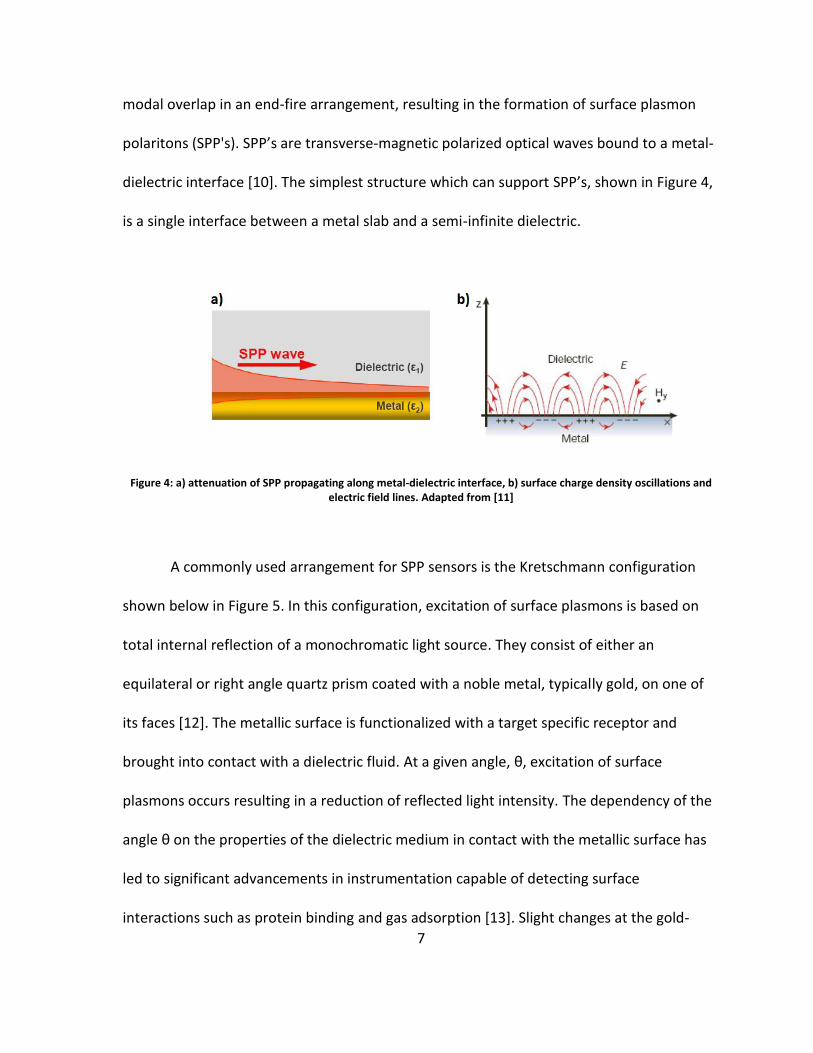
modal overlap in an end-fire arrangement, resulting in the formation of surface plasmon
polaritons (SPP's). SPP’s are transverse-magnetic polarized optical waves bound to a metal-
dielectric interface [10]. The simplest structure which can support SPP’s, shown in Figure 4,
is a single interface between a metal slab and a semi-infinite dielectric.
Figure 4: a) attenuation of SPP propagating along metal-dielectric interface, b) surface charge density oscillations and electric field lines. Adapted from [11]
A commonly used arrangement for SPP sensors is the Kretschmann configuration
shown below in Figure 5. In this configuration, excitation of surface plasmons is based on
total internal reflection of a monochromatic light source. They consist of either an
equilateral or right angle quartz prism coated with a noble metal, typically gold, on one of
its faces [12]. The metallic surface is functionalized with a target specific receptor and
brought into contact with a dielectric fluid. At a given angle, θ, excitation of surface
plasmons occurs resulting in a reduction of reflected light intensity. The dependency of the
angle θ on the properties of the dielectric medium in contact with the metallic surface has
led to significant advancements in instrumentation capable of detecting surface
interactions such as protein binding and gas adsorption [13]. Slight changes at the gold-

8
external medium interface, such as changes in refractive index due to analyte-receptor
interactions , lead to a change in the SPR signal allowing for precise measurement of thin
film properties and molecular interactions in real time.
Figure 5: Kretschmann Prism schematic
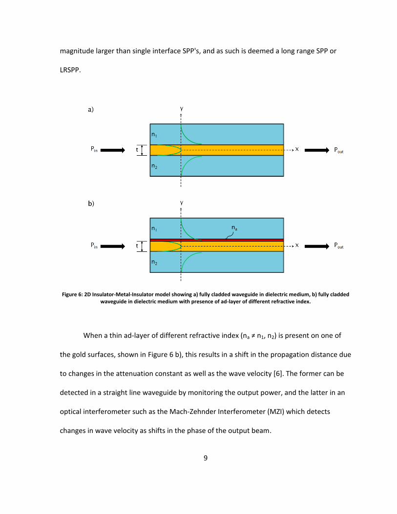
The structure of particular interest for the devices described in this thesis is the ideal
insulator-metal-insulator structure, shown in Figure 6 a). In this mode of operation, a thin
metal film of thickness t is bound at both surfaces by a dielectric medium of identical
refractive index (n1 = n2). This results in coupling of two single interface SPP's forming
symmetric and asymmetric supermodes. Based on theory ([14], [15]), the symmetric
supermode is capable of much longer propagation distances, as much as 1 or 2 orders of
9
magnitude larger than single interface SPP's, and as such is deemed a long range SPP or
LRSPP.
Figure 6: 2D Insulator-Metal-Insulator model showing a) fully cladded waveguide in dielectric medium, b) fully cladded waveguide in dielectric medium with presence of ad-layer of different refractive index.
When a thin ad-layer of different refractive index (na ≠ n1, n2) is present on one of
the gold surfaces, shown in Figure 6 b), this results in a shift in the propagation distance due
to changes in the attenuation constant as well as the wave velocity [6]. The former can be
detected in a straight line waveguide by monitoring the output power, and the latter in an
optical interferometer such as the Mach-Zehnder Interferometer (MZI) which detects
changes in wave velocity as shifts in the phase of the output beam.

10
Ideally, a structure is desired to have the lowest attenuation value possible since
waveguide-based sensor sensitivity is proportional to sensor length [6],[15]. This concept
applies to straight waveguides as well as MZI's, shown in Figure 7 a) and b) respectively. The
longer the sensing arms of an MZI, the higher the sensor sensitivity. In a scenario free of
losses, the sensitivity will increase indefinitely with sensor length for both types of
structures [6].
Figure 7: Waveguide based sensor structures with etched fluidic channels: a) Straight waveguide, b) Mach-Zehnder interferometer (MZI). Adapted from [6].
The purpose of the fluidic channels shown in Figure 7 is to be able to expose the
gold waveguide surface to a sensing medium. In the case of MZI sensors, one arm is
exposed to the sensing medium while the other arm is left fully cladded in the dielectric.
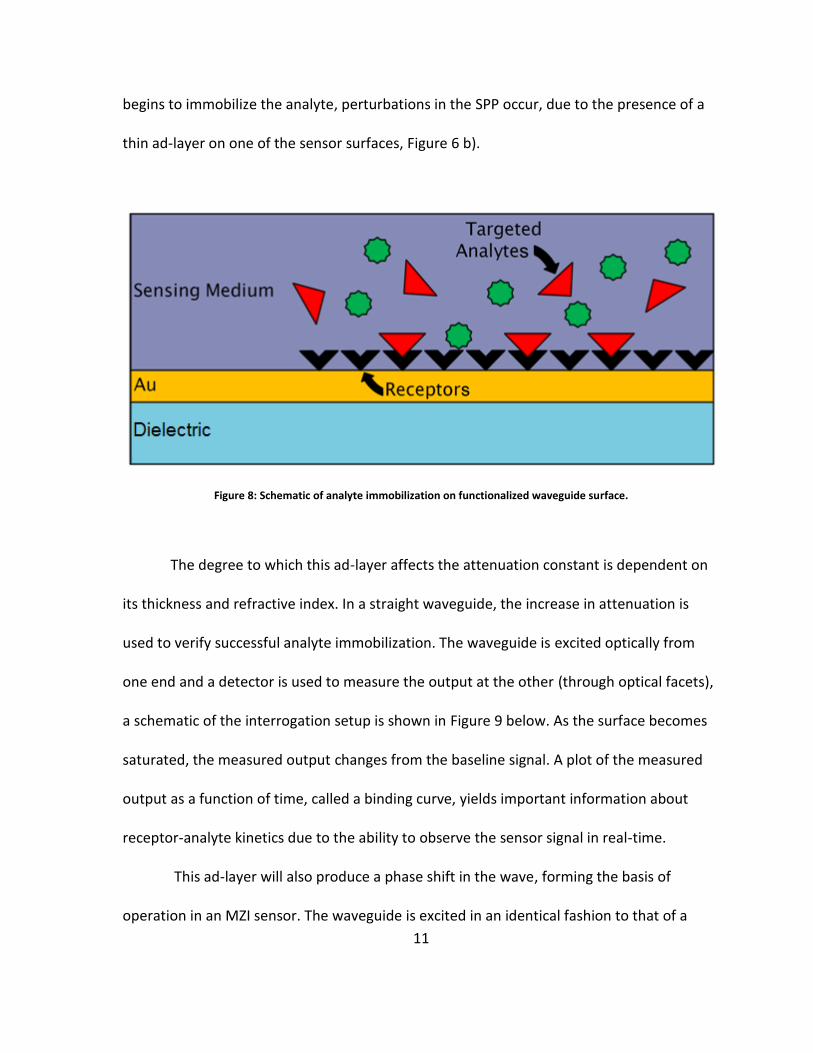
The exposed, or sensing, arm is functionalized with target specific receptor molecules such
that it is able to immobilize the desired analyte, shown in Figure 8. As the sensor surface
11
begins to immobilize the analyte, perturbations in the SPP occur, due to the presence of a
thin ad-layer on one of the sensor surfaces, Figure 6 b).
Figure 8: Schematic of analyte immobilization on functionalized waveguide surface.
The degree to which this ad-layer affects the attenuation constant is dependent on
its thickness and refractive index. In a straight waveguide, the increase in attenuation is
used to verify successful analyte immobilization. The waveguide is excited optically from
one end and a detector is used to measure the output at the other (through optical facets),
a schematic of the interrogation setup is shown in Figure 9 below. As the surface becomes
saturated, the measured output changes from the baseline signal. A plot of the measured
output as a function of time, called a binding curve, yields important information about
receptor-analyte kinetics due to the ability to observe the sensor signal in real-time.
This ad-layer will also produce a phase shift in the wave, forming the basis of
operation in an MZI sensor. The waveguide is excited in an identical fashion to that of a

12
straight waveguide, the wave travels along the straight portion and its power is split equally
amongst each of the MZI arms as the wave leaves the Y-junction. The sensing arm
experiences the phase shift due to analyte immobilization, while the cladded, or reference,
arm maintains the same phase as the power source. As both waves approach the Y-junction
on the opposite end of the structure, they are coupled together and the phase shift in the
coupled wave can be detected indicating the presence of an analyte.
Figure 9: Optical interrogation setup schematic.
1.3. Device Structure & Operation
The procedure outlined in this paper is for the fabrication of long range surface
plasmon polariton waveguides with the incorporation of micro-fluidic channels for
biosensing applications. The waveguides are thin stripe gold waveguides with dimensions
measuring 5 µm in width and 35 nm in thickness. These devices are bound between two
thick layers of CYTOP (registered trademark of Asahi Glass Corporation, Tokyo, Japan) with
a minimum dimension of 8 µm in thickness, top and bottom. CYTOP is selected as the
13
dielectric material in these devices for several reasons. It is impervious to water, oil and
most chemical substances with exception to a specific fluorocarbon solvent provided by the
manufacturer (Asahi Glass Corporation). CYTOP can be easily applied by means of spin
coating, dip coating and potting. Furthermore, of most interest is its refractive index. CYTOP
has a refractive index slightly above that of water. This allows for the fluidic channels to be
filled with dilute aqueous solutions and still allow for the waveguides to maintain a
symmetric mode of operation, and for the fluidic channels to disappear optically. The
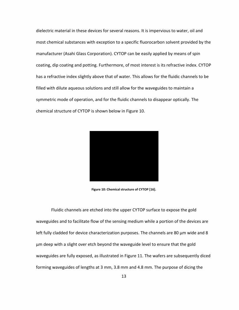
chemical structure of CYTOP is shown below in Figure 10.
Figure 10: Chemical structure of CYTOP [16].
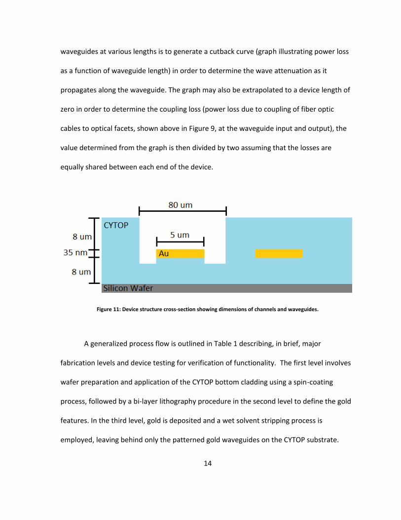
Fluidic channels are etched into the upper CYTOP surface to expose the gold
waveguides and to facilitate flow of the sensing medium while a portion of the devices are
left fully cladded for device characterization purposes. The channels are 80 µm wide and 8
µm deep with a slight over etch beyond the waveguide level to ensure that the gold
waveguides are fully exposed, as illustrated in Figure 11. The wafers are subsequently diced
forming waveguides of lengths at 3 mm, 3.8 mm and 4.8 mm. The purpose of dicing the
14
waveguides at various lengths is to generate a cutback curve (graph illustrating power loss
as a function of waveguide length) in order to determine the wave attenuation as it
propagates along the waveguide. The graph may also be extrapolated to a device length of
zero in order to determine the coupling loss (power loss due to coupling of fiber optic
cables to optical facets, shown above in Figure 9, at the waveguide input and output), the
value determined from the graph is then divided by two assuming that the losses are
equally shared between each end of the device.
Figure 11: Device structure cross-section showing dimensions of channels and waveguides.
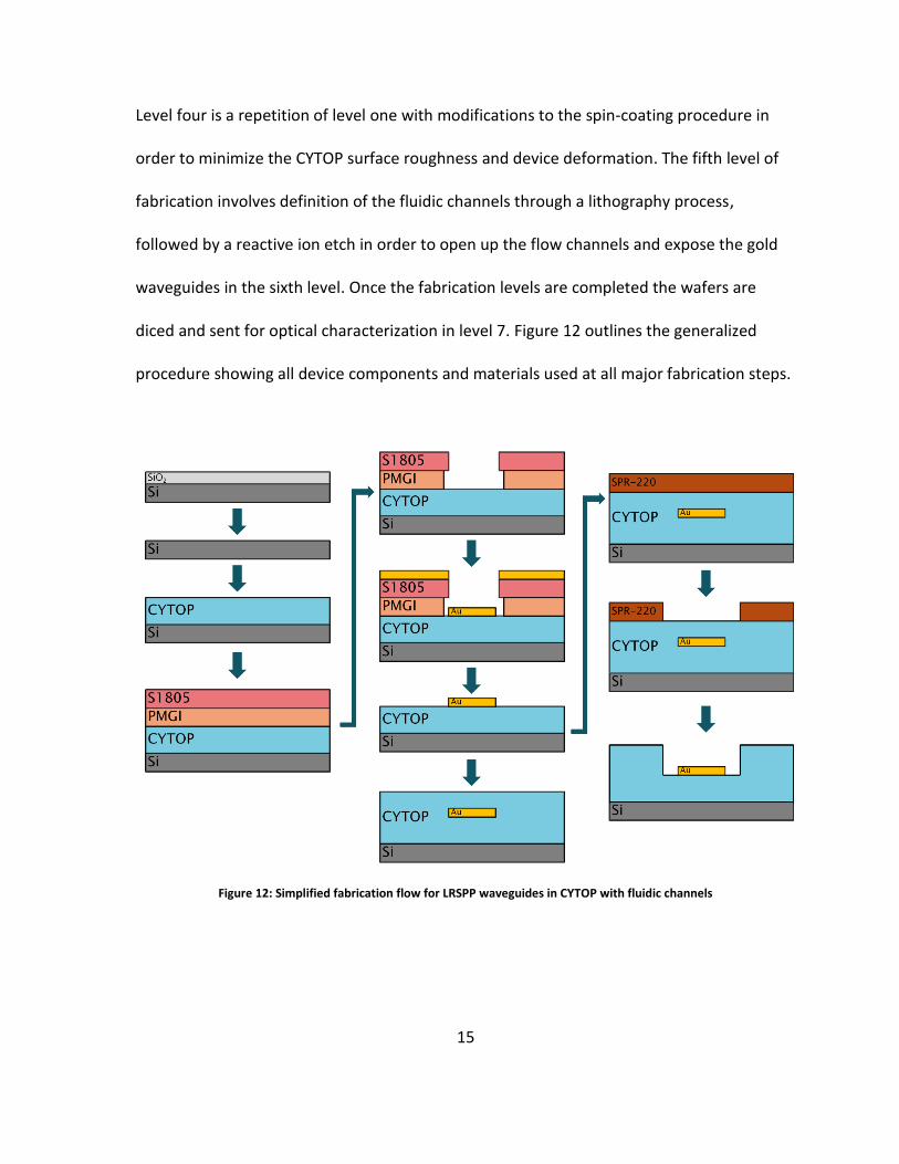
A generalized process flow is outlined in Table 1 describing, in brief, major
fabrication levels and device testing for verification of functionality. The first level involves
wafer preparation and application of the CYTOP bottom cladding using a spin-coating
process, followed by a bi-layer lithography procedure in the second level to define the gold
features. In the third level, gold is deposited and a wet solvent stripping process is
employed, leaving behind only the patterned gold waveguides on the CYTOP substrate.
15
Level four is a repetition of level one with modifications to the spin-coating procedure in
order to minimize the CYTOP surface roughness and device deformation. The fifth level of
fabrication involves definition of the fluidic channels through a lithography process,
followed by a reactive ion etch in order to open up the flow channels and expose the gold
waveguides in the sixth level. Once the fabrication levels are completed the wafers are
diced and sent for optical characterization in level 7. Figure 12 outlines the generalized
procedure showing all device components and materials used at all major fabrication steps.
Figure 12: Simplified fabrication flow for LRSPP waveguides in CYTOP with fluidic channels

16
Table 1: Generalized fabrication procedure. Adapted from [6].
Step Description Details
Device Level
1 Bottom cladding of CYTOP on Si substrate wafers
Cladded through the process of spin-
coating
2 Lithography of stripe devices Bi-layer lithography used for proper realization of gold devices
3 Gold deposition and resist strip E-beam metal deposition and wet solvent strip
Channel Level
4 Top cladding of CYTOP on stripe devices
Embeds devices in CYTOP through spin-coating
5 Lithography of microfludic channels on CYTOP claddings
Aligned to device level lithography for proper placement of channels
6 Patterned etch of stripe devices Top CYTOP claddings are dry etched with plasma
Device Characterization
7 Optical characterization Testing attenuation and insertion losses
1.4. Thesis Structure & Objectives
The primary objective of this thesis is to expand upon the works carried out by Chiu
et. al. 2009 [6], in which a fabrication procedure for similar devices was developed.
Specifically, the goal is to improve upon the quality of the various device structures, as well
as to improve the quality of the gold film of which the waveguides are comprised. The
17
desired purpose of these devices is to act as a low cost, high sensitivity replacement to
conventional immunoassays used for medical and environmental monitoring.
The main issues surrounding the fabrication procedure outlined in [6] are poor
definition of the Y-Junctions on the MZI's, over development of the lift-off resist resulting in
premature lifting of narrow structures intended to define the waveguides, poor surface
quality of the evaporated gold film due to deposition of large spits and finally deformation
of the gold features due to solvent ingress into the lower cladding during application of the
upper cladding.
It is hypothesized that the aforementioned issues may be resolved by the following
process adjustments. Firstly, replacing the current lift-off resist with a polymer which has a
reduced dissolution rate when exposed to the same developer solution will aid in improving
resolution in the Y-Junctions as well as retarding over development and premature lifting of
defining structures. Secondly, by altering the gold deposition procedure to allow for the
power to be slowly ramped up to gradually reach the desire deposition rate as opposed to
starting the procedure at an elevated power and rapidly reducing the power to reach the
desired deposition rate to eliminate "spits" on the gold surface. Finally, reducing the solvent
concentration in each layer of the upper cladding before addition of subsequent layers by
using higher temperature bakes to anneal the CYTOP, serving to minimize the diffusion rate
and thus reduce the level of deformation in the devices.
All process adjustments are monitored qualitatively through visual inspection under
an optical microscope and coupled with quantitative measurements such as atomic force

18
microscopy (AFM) scans and optical intensity measurements to verify both physical and
optical characteristics of the devices respectively.
For ease of understanding, this thesis will divide the fabrication of gold stripe
waveguides in CYTOP into four main sections:
Chapter 2 - Wafer Preparation and Lower Cladding
Describing the surface preparation of the wafer and subsequent spin
coating of the CYTOP lower cladding (unaltered from [6])
Chapter 3 - Lithography and Metallization
Describing the procedure for definition and realization of gold stripe
waveguides over CYTOP bottom cladding
Outlining changes made in lift-off resist to reduce dissolution rate and
changes made to metallization procedure to eliminate "spits" on gold
surface
Chapter 4 - Top Cladding
Describing the spin coating procedure of CYTOP for embedding of gold
stripe waveguides
Outlining modifications implemented in order to minimize rate of
solvent ingress beneath the device layer to reduce deformation of
waveguides
Chapter 5 - Flow Channels
Describing the definition and subsequent etching of the flow channels
to expose the sensing surface (unaltered from [6])
Examining the physical and optical characteristics of the devices and
briefly outlining testing procedures used to verify quality and
operability of optical waveguides
Each chapter will provide a detailed description of the steps necessary for realization
of the desired devices followed by a characterization of the features of interest.
Furthermore, chapters 3, 4 and 5 will show comparative results of devices fabricated using

19
a previously developed procedure [6] and outline the improvements achieved in device
quality and functionality.

20
2. Wafer Preparation and Bottom Cladding
2.1. Objectives
The following chapter outlines the procedure for preparation of the wafers prior to
beginning the actual fabrication procedure as well as the application process used for
constructing the lower CYTOP cladding. The procedures described within this chapter are
unchanged from those depicted in Chiu et. al. 2009 and serve mainly for consistency
purposes of the fabrication procedure.
2.2. Wafer Cleaning and Preparation
All devices are constructed on 4 inch silicon wafers with a <1,0,0> crystallographic
structure. This is verified by inspecting the alignment of the flat edges on the wafer,
specifically, by insuring that the large flat edge on the bottom of the wafer is either parallel
to a short flat edge on the top of the wafer, Figure 13 a), or perpendicular to a short flat
edge on the left side of the wafer, Figure 13 b).
Figure 13: Flat alignment for wafer crystallographic orientation verification, a) showing parallel secondary flat, b) showing perpendicular secondary flat.

21
The wafers are prepared by first immersing them in 10 wt% aqueous hydrofluoric
acid for 20 seconds in order to remove any SiO2 from the surface. Afterwards they are
rinsed in demineralised/deionised water and dried under a high purity nitrogen jet. The
wafers are then etched in O2 plasma to dehydrate the surface and remove any surface
contaminants that may have survived the HF dip. The plasma etch conditions are given in
Table 2 shown below.
Table 2: Wafer preparation O2 plasma etch specifications
Machine make and model Plasmatic Systems - Plasma-preen II 862
Power (W) 750
Oxygen flow rate (sccm) 300
Operating pressure (Torrg) 5
Exposure Time (min) 5
After the cleaning and dehydration in O2 plasma, the wafer is again exposed to a
high purity nitrogen jet to ensure that no dust particles are present on the polished surface.
2.3. Lower Cladding Fabrication
Once the wafer surface is clean and dry, the bottom cladding process may be
applied (the lower cladding fabrication process described in [6] is adequate and was applied
in this thesis without modification). This begins with a thin layer of M-grade CYTOP (CTL-
809M) diluted down to 5 wt% solids using CT SOLV 180 as the diluent. M-grade CYTOP

22
incorporates a silanated end-group adhesion promoter to facilitate bonding to a silicon
substrate, shown in Figure 14 below.
Figure 14: Schematic of silanated end-group of M-grade CYTOP for adhesion promotion to silicon substrates [16].
This layer is spin coated, initially at 500 rpm for 10 seconds to ensure proper
coverage of the wafer, then 1000 rpm for an additional 20 seconds to achieve the desired
thickness of approximately 400 nm [6]. After spinning, the wafer is "soft baked" on a direct
contact hot plate at 50 °C for 30 minutes. This removes the majority of the solvent from the
CYTOP layer allowing for easier handling during subsequent processing steps.
Once the initial M-grade adhesion layer is applied, the bulk of the bottom cladding is
spun on using S-grade CYTOP (CTX-809SP2) at 9 wt% solids. S-grade CYTOP is spun at 1000
rpm for 10 seconds to ensure full wafer coverage then ramped up to 1500 rpm for an
additional 20 seconds to achieve the desired layer thickness of 2.35 µm [6]. The wafer is
then subjected to another 30 minute "soft bake" at 50 °C to partially anneal the film. The
spinning and baking process is repeated two more times in order to obtain a total cladding

23
thickness of S-grade CYTOP of approximately 7 µm, this insures that the initial M-grade
CYTOP layer and the polished silicon wafer surface are outside of the optical tail of the
propagating waves. The need for multiple layers is to ensure that each layer is spun on
smoothly and with little to no surface defects, this is difficult if spinning at low velocities
and thus requires multiple coatings.
The final bottom cladding layer is applied using S-grade CYTOP diluted down to 5
wt% solids using CT SOLV 180 as the diluent. This is done to ensure that the CYTOP-metal
interface maintains the desired optical properties of S-grade CYTOP while also minimizing
surface variation in the bottom cladding due to the reduced viscosity of diluted CYTOP. The
layer is spun at 1000 rpm for 20 seconds giving a film thickness of approximately 0.76 µm
[6]. After spinning, the wafer is then placed on a direct contact hot plate at 50 °C for 30
minutes. Once the final layer is "soft baked", the hot plate is then ramped up from 50 °C to
200 °C at a rate of 150 °C/hr then maintained at 200 °C for an additional 2.5 hours. This fully
anneals the CYTOP bottom cladding as well as helps planarization of the upper surface. The
full bottom cladding process is illustrated in Figure 15 and described in Table 3.

24
Figure 15: Wafer priming and bottom cladding fabrication process flow diagram

25
Table 3: Wafer priming and bottom cladding fabrication procedure
Processing Step Description
HF Dip Wafer dipped into 10 wt% HF to remove native SIO2 layer from wafer surface
Plasma Preen Wafer Priming Wafer dehydration and cleaning in microwave induced O2 plasma
5 wt% solids CTL-809M spin coating
Spread-spin at 500 rpm for 10 seconds followed by planarizing-spin at 1000 rpm for 20 seconds (0.4 µm)
Soft bake 30 minute bake direct contact hot plate at 50°C
9 wt% solids CTX-809SP2 spin coating
Spread-spin at 1000 rpm for 10 seconds followed by planarizing-spin at 1500 rpm for 20 seconds (2.35 µm)
Soft Bake 30 minute bake direct contact hot plate at 50°C
9 wt% solids CTX-809SP2 spin coating
Spread-spin at 1000 rpm for 10 seconds followed by planarizing-spin at 1500 rpm for 20 seconds (2.35 µm)
Soft Bake 30 minute bake direct contact hot plate at 50°C
9 wt% solids CTX-809SP2 spin coating
Spread-spin at 1000 rpm for 10 seconds followed by planarizing-spin at 1500 rpm for 20 seconds (2.35 µm)
Soft Bake 30 minute bake direct contact hot plate at 50°C
5 wt% solids CTX-809SP2 spin coating
Planarizing-spin at 1000 rpm for 20 seconds (1.4 µm)
Soft Bake 30 minute bake direct contact hot plate at 50 °C
Hard Bake Ramp from 50 °C to 200 °C at 150 °C/hr then hold for additional 2.5 hours at 200 °C (3.5 hr total)

26
In the aforementioned procedure, the most important control variables are the spin
speeds and CYTOP concentrations. This will ensure that the deposited film is of sufficient
thickness which is vital for proper operation of the waveguides [14]. Furthermore, the
CYTOP concentration will determine the degree of planarization of the upper surface, since
this is the supporting structure of the waveguides it is important to have a smooth, flat
surface in order to minimize any deformation which may occur in the metal structure.
2.4. Surface Characterization
The surface roughness of the bottom cladding was verified using atomic force
microscopy (AFM) [6]. A 3 µm × 3 µm patch is analyzed in order to check for root-mean-
square (rms) and average surface roughness, shown in Figure 16. The CYTOP surface was
shown to have a rms roughness of 0.81 nm and an average surface roughness of 0.6 nm.
According to simulation studies performed in [14], a maximum surface roughness of 1 nm is
required in order for proper functionality of waveguides.
Another important aspect to be measured is the refractive index of the bottom
cladding. CYTOP is selected as the dielectric material in these devices due to the proximity
of its refractive index to water. Since many biosensing applications are performed using
dilute aqueous solutions, this property makes CYTOP an ideal choice. S-grade CYTOP is
reported to have a refractive index of 1.3395 when tested at a wavelength of 633 nm [16].
Water tested at the same wavelength yields a refractive index of 1.3330. Measurements
performed in [6] yielded an average refractive index of 1.3385 ± 0.0001 for the lower

27
cladding, since the lower cladding fabrication procedure used in the devices described in
this thesis is identical to that used in [6], it is assumed that an average value of 1.3385 is an
accurate representation of the refractive index of CYTOP.
Figure 16: AFM surface amplitude scan for roughness verification. Adapted from [6]

28
3. Lithography and Metallization
3.1. Objectives
This chapter outlines the fabrication processes involved in definition and realization
of the gold waveguides. Modifications were proposed to the original process outlined in
Chiu et. al. 2009 including substitution of the lift-off resist in order to reduce the dissolution
rate to improve Y-Junction resolution and eliminate over-development of defining
structures in double and triple output MZI's as well as reduction of the gold deposition rate
in order to eliminate spits on the gold surface.
3.2. Materials and Method
Surface Priming
After the bottom cladding is fully annealed, the CYTOP surface must be primed in order
to facilitate the application of the lift-off resist and the photoresist for waveguide definition.
Since CYTOP is highly repellent to water and oil, it must be treated to allow spin coating of
polar compounds such as solvents contained in PMGI (cyclopentanone and
tetrahydrofurfuryl alcohol) [17].
The CYTOP surface is initially primed with O2 plasma to “ash” the surface and allow for
coating of hexamethyldisilazane (HMDS) which is spun at 1000 rpm for 10 seconds then
baked on a direct contact hot plate at 105 °C for 1 minute. “Ashing” is performed in a
March Systems Jupiter II bench-top etcher, this helps improve the surface wettability

29
allowing for the application of PMGI lift-off resist. The surface priming procedure is outlined
in Table 4 below.
Table 4: CYTOP surface priming procedure for photolithography processing
Processing Step Description
Ashing O2 plasma etch at 100 W, 300 mTorr and 220 sccm for 30 seconds
HMDS Spinning Spin coating of HMDS (1000 rpm for 10 seconds)
Soft Bake Bake on direct contact hot plate for 1 minute at 105 °C
Bi-Layer Lithography
After baking, the surface is cleaned off with high purity nitrogen then PMGI SF 2G is
spun on, initially at 500 rpm to ensure total wafer coverage, followed by 1000 rpm to
achieve the desired thickness of approximately 75 nm [17]. The wafer is then baked on a
direct contact hot plate for 3 minutes at 180 °C to dry the solvent. Following the PMGI lift-
off resist, S1805 positive tone photoresist is spun on, initially at 1000 rpm for 10 seconds,
then at 4000 rpm for an additional 30 seconds to bring the film down to a desired thickness
of approximately 600 nm. The wafer is then baked on a direct contact hot plate at 115 °C
for 3 minutes. The bi-layer lithography procedure is shown Table 5 below and in the process
drawing shown in Figure 17.
This is a revision to a previously developed procedure outlined in [6], in which a similar
approach is taken towards the spin coating of the photoresist with the exception of a

30
substitution in the lift-off resist. The previous process called for Microchem's LOR-1A lift-off
resist, spun initially at 1000 rpm for 10 seconds, then at 4000 rpm for an additional 30
seconds. The spin coating procedure is followed by baking on a direct contact hot plate at
180 °C for 3 minutes to fully cure the resist layer.
The decision to use PMGI SF 2G was primarily based on its relatively low dissolution
rate in MF 321 developer solution. This allows for good control of the undercut and yields
cleaner lift-off, giving better overall device definition. A detailed description of the
improvements achieved through the use of PMGI SF 2G as the lift-off resist is given in
section 3.3.
Table 5: Lift-off resist and photoresist application procedure
Processing Step Description
Nitrogen clean Wafer is sprayed with high purity nitrogen stream to partially dry surface as well as removing dust and other particulates.
PMGI SF 2G Spinning PMGI lift-off resist is spun at 500 rpm for 10 seconds followed by 1000 rpm for 30 seconds (~ 75 nm)
Soft Bake PMGI is baked at 180 °C for 3 minutes
S1805 Spinning S1805 positive photoresist is spun on at 1000 rpm for 10 seconds followed by 4000 rpm for 30 seconds (600 nm)
Soft Bake S1805 is baked at 115 °C for 3 minutes

31
Figure 17: Bi-layer lithography process drawing
Exposure and Development
Definition of the waveguide structures is achieved through UV exposure of the
S1805 photoresist. This is a positive tone photoresist, such that the portions of the film
exposed to UV light become susceptible to the developer solution and as such is washed
away leaving behind openings for subsequent deposition and lift-off of gold for realization
of waveguide features. Exposure is achieved with the use of a Karl-Suss mask aligner, the
specifications and prescribed exposure conditions are outlined in Table 6 below. The
required exposure for a 600 nm layer of S1805 is known to be within the range of 7 to 8

32
seconds [6], this places the exposure energy density in the range of 80 to 180 mJ/cm2 for
the given lamp intensity.
Table 6: Mask aligner specifications and exposure conditions
Mask Aligner Specifications
Make and Model Karl Suss MA6 Mask Aligner
Lamp 350 W Mercury vapour
Measured Intensity Peaks
@ 365 nm 8.4 mW/cm2
@ 405 nm 14 mW/cm2
Exposure Conditions
Exposure energy 80 - 180 mJ/cm2
Exposure time 7 - 8 seconds
The key components of the mask aligner and their orientation in relation to the
wafer surface are illustrated in Figure 18. The wafer is held horizontally, by vacuum, in a
chuck with the photoresist surface facing upwards. The device mask, portions of which are
shown in Figure 19 , is placed in direct contact with the photoresist surface having the
patterned side facing downwards. Pressure is applied mechanically by the chuck forcing the
wafer upwards in order to eliminate any air gaps which may exist at the mask-wafer
interface. Once exposure is desired, the shutter is opened allowing UV light to be guided by
the mirrors and through the condenser lens towards the device mask. The mask itself is
made of UV transparent glass, with a standard, patterned chromium film applied to the side
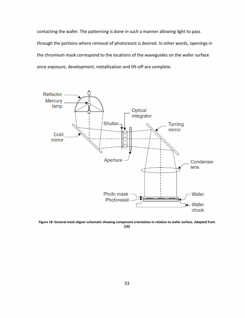
33
contacting the wafer. The patterning is done in such a manner allowing light to pass
through the portions where removal of photoresist is desired. In other words, openings in
the chromium mask correspond to the locations of the waveguides on the wafer surface
once exposure, development, metallization and lift-off are complete.
Figure 18: General mask aligner schematic showing component orientation in relation to wafer surface. Adapted from [18]

34
Figure 19: Sample device structure layout including MZI's, straight line waveguides and triple waveguides with contact pads. Adapted from [6]
The device layout shown in Figure 19 shows MZI's coupled to triple output
waveguides and alternating straight line waveguides in between. After exposure the wafer
is immersed in a room temperature bath of MF 321 developing solution, development time
takes 2.5 minutes with a moderate level of agitation applied by hand. The developer bath
removes the exposed portion of S1805 and the PMGI underneath. Since the lift-off resist is
not photo-sensitive, the developer solution will continue to dissolve beyond the regions
defined by the photoresist layer above. This is highly desirable and necessary in order for
proper realization of the gold features. Care must be taken not to over-develop the wafers
as washing out of the lift-off resist may occur; this phenomenon will be discussed in detail
in section 3.3. Figure 20 shows a S1805 layer thickness of approximately 600 nm over a

35
PMGI layer thickness of approximately 75 nm and an undercut depth of roughly similar
magnitude.
Figure 20: SEM image of developed bi-layer resist stack
During the alignment step, it is important to ensure that the waveguides are
oriented perpendicularly to the long flat edge at the bottom of the wafer, shown in Figure
13. This is to avoid any issues that may arise during dicing, by aligning the waveguides such
that the direction of propagation of the waves is at a 90 ° angle to the flat at the bottom of
the wafer, the dies can then be cut along the crystallographic planes of the wafer, thus

36
avoiding any undesirable fracturing of the wafer which may cause damage to the devices
and reduce the overall yield of the wafer. A procedural outline for exposure and
development of the wafers is given in Table 7 and shown graphically in Figure 21.
Table 7: Processing steps for exposure and development of wafer for device feature definition.
Process Step Description
Wafer Alignment The flat at the bottom of the wafer is aligned such that the waveguides run in a perpendicular direction to it
Exposure Wafer is exposed for 7 - 8 seconds under a 350 W mercury vapour bulb (80 - 180 mJ/cm2)
Development Wafer immersed in room temperature bath of MF 321 for 2.5 minutes (with medium to strong agitation approximately 75 nm of undercut is achieved, Figure 20)

37
Figure 21: Wafer exposure and development process flow diagram

38

39
Metallization and Lift-off
Gold deposition is performed in a Balzer BA510 system retrofitted with the following
pieces of equipment [19]:
CTI CryoTorr 8 Cryopump - used to achieve high vacuum in deposition
chamber
Sloan Planetary Fixture - holds wafers during deposition and is capable of
rotation as well in order to reduce variations in film thickness
Airco Temescal FDC 8000 automated deposition rate and film thickness
controller - used to vary power available to e-beam in order to control
deposition rate and film thickness
Airco Temescal CV-8 e-beam system - power source for heating of deposition
material
These retrofits allow for accurate deposition of gold onto the wafer surface with a
high degree of control and relatively low variability. Before deposition can occur, the
exposed CYTOP surface must be primed in order to provide a suitable contact area for gold
adhesion. This is done with a short, 30 second, exposure to O2 plasma. This procedure is
identical to the first step shown in Table 4, "Ashing", and serves to roughen the CYTOP
surface slightly, giving the gold more surface area to bond to. The roughening effects of O2
plasma on CYTOP are explained in further detail in section 5.3.

40
The short exposure time to the O2 plasma is sufficient to properly prime the CYTOP
surface for gold deposition while still leaving the patterned photoresist, and underlying lift-
off resist, unaltered.
Figure 22: Pre-metallization microscope image of triple waveguide structure with contact pads (dimensions shown).
Figure 22, above, shows a close-up image of a triple waveguide structure prior to
metallization; these are among the most challenging structures to fabricate on the layout
given the need for accurate dimensions in waveguide line-width and spacing. As can be
seen, the pattern remains fully intact with good resolution and proper dimensions after
"ashing" is performed. The darker, greyer portions indicate areas where the photoresist/lift-

41
off resist stack has been washed away, while the lighter, yellower portions indicate areas
that were blocked by the photo-mask and thus not susceptible to the developer solution.
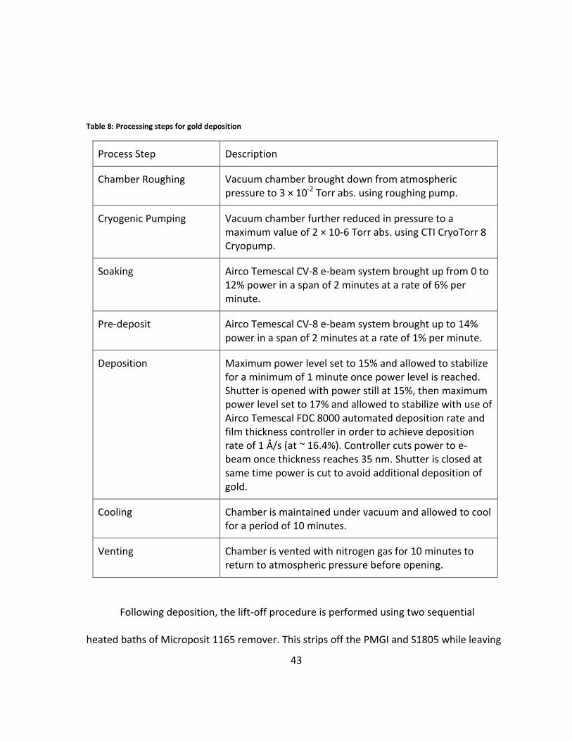
Gold deposition is performed at a rate of 1 Å/s to achieve a total film thickness of 35
nm. The wafers are suspended upside down on the Sloan planetary fixture and held in place
with magnets. The chamber is then brought under vacuum to a maximum pressure of 2 ×
10-6 Torr absolute. Once vacuum is achieved, the e-beam source is brought up to a power of
12% during the "soaking" stage at a rate of 6% per minute followed by a much slower "pre-
deposit" stage in which the power is brought up to 14% at a rate of 1% per minute. During
the deposition stage, the maximum power is initially limited to 15%, once this power level is
reached, the gold is allowed to stabilize for 1 minute, after which time the shutter is opened
and the maximum power level is raised to 17%. By raising the power after the shutter is
opened, the deposition rate is allowed to increase slowly, avoiding the formation of gold
"spits" on the surface and minimizing the amount of gold used during the deposition
process. Once deposition is complete, the shutter is closed, the power source is shut off,
the chamber is allowed to cool for a period of 10 minutes then vented with high purity
nitrogen for an additional 10 minutes in order to return the chamber to atmospheric
pressure before opening and removing the wafers.
A small opening in the centre of the Sloan planetary fixture allows for the evaporant
to deposit on a quartz crystal microbalance, which makes use of the gold density and its
acoustic impedance to determine the deposition rate and film thickness. A general

42
schematic of the evaporator system is shown in Figure 23, indicating all major components
and their orientation. The process used for deposition is outlined in Table 8, shown below.
Figure 23: E-beam evaporator schematic
43
Table 8: Processing steps for gold deposition
Process Step Description
Chamber Roughing Vacuum chamber brought down from atmospheric pressure to 3 × 10⁻² Torr abs. using roughing pump.
Cryogenic Pumping Vacuum chamber further reduced in pressure to a maximum value of 2 × 10⁻⁶ Torr abs. using CTI CryoTorr 8 Cryopump.
Soaking Airco Temescal CV-8 e-beam system brought up from 0 to 12% power in a span of 2 minutes at a rate of 6% per minute.
Pre-deposit Airco Temescal CV-8 e-beam system brought up to 14% power in a span of 2 minutes at a rate of 1% per minute.
Deposition Maximum power level set to 15% and allowed to stabilize for a minimum of 1 minute once power level is reached. Shutter is opened with power still at 15%, then maximum power level set to 17% and allowed to stabilize with use of Airco Temescal FDC 8000 automated deposition rate and film thickness controller in order to achieve deposition rate of 1 Å/s (at ~ 16.4%). Controller cuts power to e-beam once thickness reaches 35 nm. Shutter is closed at same time power is cut to avoid additional deposition of gold.
Cooling Chamber is maintained under vacuum and allowed to cool for a period of 10 minutes.
Venting Chamber is vented with nitrogen gas for 10 minutes to return to atmospheric pressure before opening.
Following deposition, the lift-off procedure is performed using two sequential
heated baths of Microposit 1165 remover. This strips off the PMGI and S1805 while leaving

44
the waveguide structures and CYTOP fully intact. The wafer is immersed in the first bath,
maintained between 70 - 80 °C, for a period of 10 minutes with no agitation. Following this
the entire 1165 bath is placed in an ultrasonic bath for 10 seconds to strip away a majority
of the gold. The wafers are then placed in a second 1165 bath, also between 70 - 80 °C, for
an additional 10 minutes followed by another ultrasonic bath for 10 seconds. At this point,
all that remains is the gold waveguides on top of the CYTOP bottom cladding (due to strong
adhesion between CYTOP and gold [6]). The wafers are then immersed in isopropyl alcohol
for 10 minutes to clean off any residue remaining after the lift-off procedure and finally
rinsed with de-ionized water to finish cleaning the surface. The lift-off procedure is outlined
in Table 9 as well as the entire deposition and lift-off procedure in Figure 24 shown below.

45
Figure 24: Gold deposition and lift-off process flow diagram

46
Table 9: Processing steps for gold lift-off
Process Step Description
Microposit 1165 Bath 1 Bath temperature raised to 70 - 80 °C, wafers immersed for 10 minutes.
Ultrasonic Bath 1 Wafer and 1165 bath placed in larger water bath and exposed to ultrasonic vibration for 10 seconds to strip off majority of lift-off resist.
Microposit 1165 Bath 2 Bath temperature raised to 70 - 80 °C, wafers immersed for 10 minutes.
Ultrasonic Bath 2 Wafer and 1165 bath placed in larger water bath and exposed to ultrasonic vibration for 10 seconds to strip off remainder of lift-off resist.
IPA Bath Wafers immersed in high purity isopropyl alcohol bath for 10 minutes.
DI Water Rinse Wafers rinsed off with de-ionized water.
Nitrogen Spray Wafers sprayed with high purity nitrogen jet to dry off water.
3.3. Results and Discussion
The deposition procedure explained above is a modification to the procedure
outlined in [6]. The purpose of the modification was to slow down the deposition rate by
performing a more gradual heating in the "deposition" stage discussed in Table 8. By
opening the shutter at only 15% power as opposed to 17% power, the deposition rate is still
at 0 Å/s. The power then slowly increases in order to achieve a rate of 1 Å/s at about 16.4%
power. The previous process had the deposition rate set to 2 Å/s and called for the shutter
to be opened after the power level had reached 17%. This resulted in a much higher initial

47
deposition rate and consequently yielded gold "spits" which were visible on the gold
surface as small, randomly dispersed dots, illustrated in Figure 25 a).
Figure 25 b), shows the gold surface generated by the new process, in which a
substantial reduction in "spits" on the gold surface is evident. AFM scans of small, 3 µm × 3
µm, patches of the gold surface for both the old and new deposition procedures are shown
in Figure 26 a) and b) respectively. The scale on the left indicates the rms roughness of 23
nm and an average roughness of 18 nm due to the presence of "spits" on the gold surface in
Figure 26 a). Comparatively, Figure 26 b) shows a gold surface generated by the modified
procedure, in which the rms roughness has been reduced to 0.7 nm and the average
roughness down to 0.5 nm. This is a drastic decrease in the waveguide roughness resulting
in a substantial improvement in optical and biological performance, evident in the
characterization of the devices in section 5.3. This is supported by claims made in [14], in
which surface and edge roughness of the devices may lead to additional losses, reducing
the wave propagation distance and consequently the device sensitivity [6], [15].
It should be noted that the contact pads shown in Figure 25, as well as in
subsequent images, serve only to allow for electrochemistry (use of potential differences to
drive chemical reactions on gold surface) and thermo-optic modulation (electrical
resistance heating of gold and surrounding medium to alter refractive indices thus changing
wave propagation characteristics). At this point the contact pads require additional
deposition of metal in order to improve robustness (35 nm too thin to withstand continual
probing with electrodes), the figures included in this thesis are used primarily due to the

48
fact that they provide a large metallic structure by which qualitative observations of the
gold surface are easily obtained.
Figure 25: Gold contact pads after lift-off a)showing spits on surface using old deposition procedure [6], b) showing no spits on surface using modified deposition procedure.

49
Figure 26: AFM images of gold surface a) showing surface with spits fabricated using old deposition procedure (rms roughness = 23 nm, avg. roughness = 18 nm). Adapted from [6]. b) showing no spits on gold surface using new
deposition procedure (rms roughness = 0.7 nm, avg. roughness = 0.5).

50
After lithography, deposition and lift-off, the metal patterns may be viewed under
high magnification. Upon close visual inspection, benefits of the changes made to the
lithography procedure become evident. As mentioned in section Error! Reference source
ot found., improvement in feature resolution by substituting the lift-off resist is realized. By
using PMGI SF 2G instead of the LOR-1A, device quality is greatly improved upon due to the
slower dissolution of the lift-off layer. If the dissolution rate is too high, then the risk of
over-development increases and feature definition is compromised. Over-development
refers to the washing out of the lift-off resist layer beneath the photoresist layer causing a
lack of structural support. This is most evident when inspecting the Y-Junctions shown in
Figure 27 a) and b) below. When using LOR-1A, the Y-Junction has a rounded profile, Figure
27 a), which may lead to an uneven split in the wave power and render the MZI structures
unusable. Reducing the dissolution rate of the lift-off resist by switching to PMGI SF 2G
yields a sharper corner profile (Figure 27 b)), producing an even distribution of optical
power between the two arms of the structure.

51
Figure 27: 2 micron Y-Junction of MZI, a) fabricated using LOR-1A lift-off resist, b) fabricated using PMGI SF 2G lift-off resist.
The cause of the rounded edge profile in Figure 27 a) was determined to be washing
out, or over development of the lift-off resist near the split. This results in excessive loss of

52
structural support below the patterned photoresist, and as such, causes the photoresist to
fall out of position, as shown below in Figure 28. A representative schematic of this
phenomenon is also shown in Figure 29. Figure 28 also shows very poor edge roughness of
defining structures when LOR-1A is used as the lift-off resist.
Figure 28: SEM image of Y-Junction produced using LOR-1A showing wilting of upper layer due to loss of support from overdevelopment of lift-off layer.

53
Figure 29: Representative schematic of patterning layer wilting due to washing out of LOR-1A
The differences between the dissolution rates of various lift-off resists offered by
Microchem can be seen in below in Table 10. As the table indicates, the PMGI slow series
polymer develops at a rate of approximately one fourth to that of the LOR A class polymer
when baked at 190 °C.
Table 10: Relative dissolution rates and prebake temperature dependency of Microchem lift-off resists [20].
Prebake Temperature
(°C)
Relative Dissolution Rate (Å/s)
LOR A LOR B PMGI Fast PMGI Medium PMGI Slow
150 111 333 83 56 21
170 67 222 42 28 14
190 42 167 28 17 10
* Developer used contains 2.38% TMAH (tetramethylammonium hydroxide), MF 321 contains 1.91% TMAH. Dissolution rates assumed to be linearly proportional to TMAH content.
54
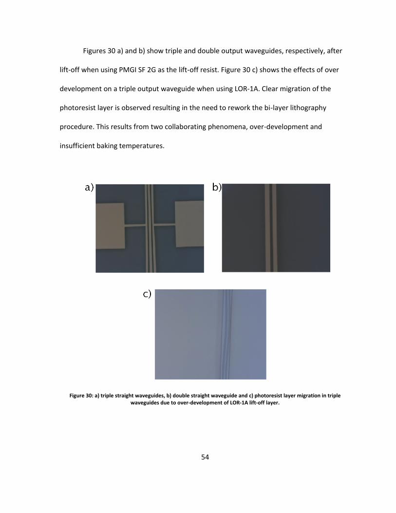
Figures 30 a) and b) show triple and double output waveguides, respectively, after
lift-off when using PMGI SF 2G as the lift-off resist. Figure 30 c) shows the effects of over
development on a triple output waveguide when using LOR-1A. Clear migration of the
photoresist layer is observed resulting in the need to rework the bi-layer lithography
procedure. This results from two collaborating phenomena, over-development and
insufficient baking temperatures.
Figure 30: a) triple straight waveguides, b) double straight waveguide and c) photoresist layer migration in triple waveguides due to over-development of LOR-1A lift-off layer.

55
The dissolution rate of the lift-off resist is strongly affected by the baking
temperature; by increasing the baking temperature, a larger amount of solvent may be
driven from the film, aiding in the densification process. As the film density increases, so
does its resistance to dissolution by the developer solution, as indicated by Table 10. In the
procedure outlined in Table 5, the baking temperature of the lift-off resist is set to 180 °C,
this is despite the manufacturer's recommendation to perform the baking step at a
minimum temperature of 185 °C [21]. By baking below the recommended temperature,
there may be a residual amount of solvent still trapped within the polymer matrix (LOR-1A
or PMGI SF 2G films), resulting in a lower film density than intended. This will effectively
reduce the lift-off layers resistance to the developer solution, leading to further
complications with over-development and adding to the reasons for switching to a slower
dissolving polymer.

56
4. Top Cladding
4.1. Objectives
This chapter outlines the application procedure for the upper CYTOP cladding,
necessary for formation of the fluidic channels used to allow passage of the sensing
medium over the gold waveguides previously discussed. The procedure outlined is based
primarily on a similar procedure described in Chiu et. al 2009, with modifications made to
the baking temperature used in between the spin coating of each additional layer of CYTOP.
The motivation behind the modifications was due to an excessive amount deformation in
the thin gold film which may adversely affect the waveguide operation. By increasing the
baking temperature of each CYTOP layer prior to application of the subsequent layer, the
amount of solvent may be minimized effectively reducing the diffusion rate of solvent
further beneath the device layer (see Appendix C for detailed diffusion characterization).
4.2. Materials and Methods
The upper CYTOP cladding is deposited in a similar fashion to that of the lower
cladding described in section 2.3, with a few important modifications to improve the gold
waveguide quality. Before spin coating, the surface must be prepared to facilitate adhesion
of the new CYTOP layer to that below the devices. This is achieved with an O2 plasma etch
carried out at 100 W, 300 mTorr and 220 sccm of O2. The wafer surface is exposed to the O2
plasma for a period of 30 seconds, which is identical to the "ashing" procedure outlined in
Table 4 and serves the same purpose.

57
Following the surface preparation, the first layer of the top cladding may be applied.
This is done by spin coating a thin layer of CTX-809SP2 (S-grade CYTOP) using a 1000 rpm
spread spin for 10 seconds followed by a planarizing spin at 4000 rpm for 20 seconds. This
layer is then baked at 50 °C for 30 minutes on a direct contact hot plate. The hot plate is
then ramped up from 50 °C to 100 °C at a rate of 25 °C/hr then maintained at 100 °C for an
additional 4 hours. This yields an approximate layer thickness of 1.1 µm of CYTOP [16]. This
process is repeated an additional 6 times with a 30 second O2 plasma etch before each
additional layer is spun on. It has been observed in some samples that small gas pockets
form between hard baked layers of CYTOP when the wafer is placed under vacuum,
specifically in the plasma etching chamber. This effect has been noted to be reduced
significantly, if not eliminated entirely, when the substrate layer has gone through an
“ashing” step prior to spin coating.
By the 7th layer, a total upper cladding thickness of 7.7 µm is achieved. The entire
procedure, which is a modification of the upper cladding process described in [6], is
outlined in Table 11 and illustrated in Figure 31. The main alteration is the addition of a high
temperature bake following the spin coating of each layer. This serves to minimize the
amount of solvent in the CYTOP prior to application of each additional coat.
CYTOP has a glass transition temperature of 108 °C, and since the baking
temperature of the top cladding is limited to 100 °C, there is still a small amount of solvent
trapped in the layer. In the previous process [6], the bake temperature between layers was
limited to 50 °C followed by a single high temperature bake after the final layer was

58
deposited. By increasing the bake temperature between layers, a noticeable improvement
in device quality was observed after the top cladding was applied. The original process
showed significant waveguide deformation due to solvent seeping underneath the gold film
(into the lower cladding); this problem will be discussed in detail in section 4.3.
Table 11: Upper cladding fabrication procedure.
Process Step Description
Şurface Prep 30 sec O2 plasma etch at 100 W, 300 mTorr and 220 sccm
1st Spin Coat CTX-809SP2 spun at 1000 rpm for 10 sec then 4000 rpm for 20 sec
1st Bake Bake at 50 °C for 30 min, ramp at 25 °C/hr for 2 hrs then hold at 100 °C for 4 hrs. Follow with 30 sec O2 plasma etch at 100 W, 300 mTorr and 220 sccm
2nd Spin Coat
CTX-809SP2 spun at 1000 rpm for 10 sec then 4000 rpm for 20 sec
2nd Bake Bake at 50 °C for 30 min, ramp at 25 °C/hr for 2 hrs then hold at 100 °C for 4 hrs. Follow with 30 sec O2 plasma etch at 100 W, 300 mTorr and 220 sccm
3rd Spin Coat CTX-809SP2 spun at 1000 rpm for 10 sec then 4000 rpm for 20 sec
3rd Bake Bake at 50 °C for 30 min, ramp at 25 °C/hr for 2 hrs then hold at 100 °C for 4 hrs. Follow with 30 sec O2 plasma etch at 100 W, 300 mTorr and 220 sccm
4th Spin Coat CTX-809SP2 spun at 1000 rpm for 10 sec then 4000 rpm for 20 sec
4th Bake Bake at 50 °C for 30 min, ramp at 25 °C/hr for 2 hrs then hold at 100 °C for 4 hrs. Follow with 30 sec O2 plasma etch at 100 W, 300 mTorr and 220 sccm
5th Spin Coat CTX-809SP2 spun at 1000 rpm for 10 sec then 4000 rpm for 20 sec
5th Bake Bake at 50 °C for 30 min, ramp at 25 °C/hr for 2 hrs then hold at 100 °C for 4 hrs. Follow with 30 sec O2 plasma etch at 100 W, 300 mTorr and 220 sccm
6th Spin Coat CTX-809SP2 spun at 1000 rpm for 10 sec then 4000 rpm for 20 sec
6th Bake Bake at 50 °C for 30 min, ramp at 25 °C/hr for 2 hrs then hold at 100 °C for 4 hrs. Follow with 30 sec O2 plasma etch at 100 W, 300 mTorr and 220 sccm
7th Spin Coat CTX-809SP2 spun at 1000 rpm for 10 sec then 4000 rpm for 20 sec

59
7th Bake Bake at 50 °C for 30 min, ramp at 25 °C/hr for 2 hrs then hold at 100 °C for 4 hrs. Follow with 30 sec O2 plasma etch at 100 W, 300 mTorr and 220 sccm

60
Figure 31: CYTOP upper cladding process flow diagram.

61
It should be noted that a total of 7 upper cladding layers are used in order to
achieve a minimum thickness of 7.7 µm. Due to the substantial reduction of solvent trapped
in the cladding, it is possible to deposit as many as 18 layers giving a total upper cladding
thickness of approximately 20 µm. This will potentially allow for realization of deeper flow
channels leading to the capability of sensing larger analytes such as white blood cells and
bacteria.
4.3. Results and Discussion
In order for the devices to be able to support LRSPP's, they must be fully bound in a
dielectric medium such that both upper and lower surfaces of the waveguides are in
contact with media of identical refractive index. Furthermore, the material must be easily
and selectively removable to allow for access to the gold surface via microfluidic channels.
For these reasons, amongst others, CYTOP is used as the dielectric material in these
devices. CYTOP is received as a 9 wt% solids solution and is applied to the wafer by means
of spin coating. This process requires a high solvent content to allow for smooth, planar
surfaces and sufficient polymer chain migration across CYTOP to CYTOP interfaces to
prevent delamination.
The CYTOP solvent, CTSOLV 180, is removed from the film by baking on a hot plate.
This process is slow and allows the solvent sufficient time to seep into previously deposited
layers below. Throughout the bottom cladding fabrication procedure, this phenomenon is
of little relevance, providing simply the means for entanglement of polymer chains between

62
the CYTOP layers, ultimately having no effect on the quality of the final structure.
Conversely, once the gold waveguides have been patterned and deposited, solvent ingress
becomes a much more relevant issue during formation of the upper cladding and may have
significant effects on the waveguide structure.
The bottom cladding is baked at 200 °C, this temperature is well above the glass
transition temperature of CYTOP resulting in complete removal of the solvent. This gives a
slow initial rate of diffusion of solvent from the top cladding layers into the bottom
cladding, as additional layers are spun on to build up the upper cladding thickness, the
solvent begins to accumulate below the device level, deforming the gold structures.
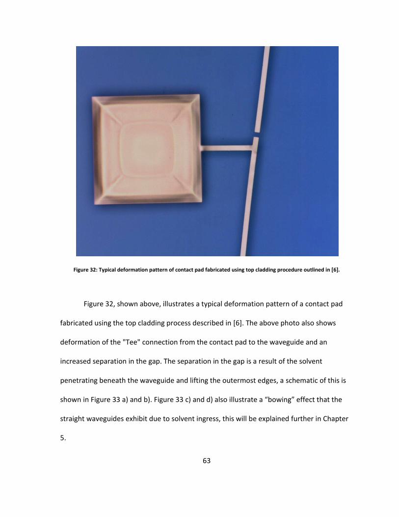
63
Figure 32: Typical deformation pattern of contact pad fabricated using top cladding procedure outlined in [6].
Figure 32, shown above, illustrates a typical deformation pattern of a contact pad
fabricated using the top cladding process described in [6]. The above photo also shows
deformation of the "Tee" connection from the contact pad to the waveguide and an
increased separation in the gap. The separation in the gap is a result of the solvent
penetrating beneath the waveguide and lifting the outermost edges, a schematic of this is
shown in Figure 33 a) and b). Figure 33 c) and d) also illustrate a “bowing” effect that the
straight waveguides exhibit due to solvent ingress, this will be explained further in Chapter
5.

64
Figure 33: Schematic illustrating separation of 2 µm gap a) before top cladding application, b) after top cladding application, c) straight waveguide prior to upper cladding application, d) straight waveguide after upper cladding
application.
After the first layer of the top cladding is applied, there is little to no apparent
deformation of the devices when using either the old [6] or the new (described herein)
procedure. This is likely due to the large difference between the molecular diffusion rate at
the bottom surface and the convective diffusion rate at the upper surface. Once the second
layer is applied, however, the impact of the solvent content within the first layer becomes
apparent. Figure 34 illustrates the extent of deformation early in the top cladding
fabrication process. The difference is a result of two collaborating conditions, the first being
the residual solvent content within the previously deposited CYTOP layer and the second
being the temporary reversal of the solvent concentration gradient. Of these two
conditions, the only one that can be rectified by adjusting the processing conditions is the
solvent concentration. By reducing the concentration in the layers closest to the devices,

65
the diffusion rate can be significantly reduced when the concentration gradient of solvent is
temporarily reversed during application of the subsequent layers.
Figure 34: Difference in device deformation after 2nd layer of top cladding a) using old procedure [6], b) using new procedure.
The reversal of the concentration gradient is illustrated in the schematic diagrams
shown below. Figure 35, using the old upper cladding fabrication procedure [6], compared
to Figure 36, using the new upper cladding fabrication procedure, has a substantially higher
residual solvent content in the first upper cladding layer. As the second layer is deposited,
the solvent concentration at the upper surface of the first layer goes from being effectively

66
zero to 91% by weight. Until the solvent concentration in the second layer is reduced to an
equivalent value of the solvent concentration in the first layer, solvent will be forced to
diffuse inwards into the bottom cladding, resulting in swelling of the CYTOP and ultimately
forcing the gold devices to deform and shift from their desired positions. This effect is
compounded with the application of each additional layer and, while being unavoidable,
can be reduced by minimizing the solvent content in the layers closest to the gold devices,
thus reducing the rate of solvent ingress.
Baking each layer at 100 °C as opposed to 50 °C helps to reduce the solvent content
without exceeding the glass transition temperature of CYTOP. Since the baking temperature
is still below the glass transition temperature, there is still some solvent remaining within
the upper cladding layers, albeit significantly lower than if only baked at 50 °C.

67
Figure 35: Solvent concentration profiles in CYTOP using old top cladding fabrication procedure [6]: a) Immediately after spin coating of 1
st layer of upper cladding, b) after baking of 1
st layer of upper cladding, c) immediately after spin coating
of 2nd
layer of upper cladding, d) after baking of 2nd
layer of upper cladding.

68
Figure 36: Solvent concentration profiles in CYTOP using new top cladding fabrication procedure: a) Immediately after spin coating of 1
st layer of upper cladding, b) after baking of 1
st layer of upper cladding, c) immediately after spin coating
of 2nd
layer of upper cladding, d) after baking of 2nd
layer of upper cladding.
As subsequent layers are deposited, a progression of solvent into the lower cladding
is observed resulting in a distinct deformation pattern. The difference in the extent of the
deformation between the old [6] and new processes is outlined in Figure 37 a) through f).
The contact pads shown in Figure 37 a), c) and e) are taken after baking of the 3rd, 4th and
5th upper cladding layers respectively using the old fabrication procedure [6]. The
deformation is indicative of a high solvent content in the CYTOP layers, as would be
expected when baked at low temperature. Figure 37 b), d) and f) are also taken after baking
of the 3rd, 4th and 5th upper cladding layers, this time using the new fabrication procedure.

69
The noticeable lack of deformation is due to a significantly lower solvent concentration in
the upper cladding, effectively reducing the diffusion rate of solvent into the CYTOP
beneath the devices.

70
Figure 37: Waveguide deformation comparison: a), b) 3rd
layer post-bake, c), d) 4th
layer post-bake, e), f) 5th
layer post-bake; (a), (c) and (e) old upper cladding process [6]; (b), (d) and (f) new upper-cladding process.
The modified upper cladding procedure does not begin to show signs of
deformation until the fifth layer is applied, as shown in Figure 38 below. While it would be

71
ideal to maintain the devices in their original condition, it is necessary to have a dielectric
thickness of approximately 8 µm (to fully contain the SPP waves) and, as a result, some
deformation must be tolerated.
Figure 38: Solvent ingress beneath contact pads as a function of upper cladding layer.
While the contact pads provide a good indication as to the extent of solvent ingress,
any deformation occurring in them is relatively harmless in terms of their functionality.
More sensitive features such as the Y-Junctions and the thin stripe waveguides must be
examined in order to gain insight as to the effect of solvent ingress on device operability.
y = 3.8684e0.3316x
y = 0.0016e1.2728x
0
5
10
15
20
25
30
35
40
45
1 2 3 4 5 6 7
Solv
en
t In
gre
ss f
rom
Co
nta
ct P
ad E
dge
(µ
m)
Upper Cladding Layer
Solvent Ingress vs. Upper Cladding Layer
Chiu et al. 2009
Modified Procedure

72
5. Flow Channels
5.1. Objectives
This chapter outlines the procedure used to define and etch the fluidic channels
used to expose the gold waveguide surface to allow for subsequent functionalization for
biosensing applications as well as outlining various techniques used to verify the waveguide
dimensions and operability. The channel etching process is identical to that described in
Chiu et. al. 2009, with a slight difference in the etching procedure to allow for closer
monitoring of the timed etching process in order to reduce the degree of ever-etching
beyond the waveguide level.
5.2. Channel Lithography
Once the wafers are fully cladded in CYTOP, the fluidic channels must be defined in
preparation for etching. This is achieved through a lithographic technique substantially
different from that used in defining the gold features. The first step, as in the procedure
outlined in Table 4, is an O2 plasma etch carried out at 100 W, 300 mTorr and 220 sccm of
O2. This is done for 30 seconds in order to "ash" the CYTOP surface and facilitate spin
coating of the patterning resist.
The patterning resist used for channel definition is a "MEGAPOSIT SPR 220-7"
positive tone photoresist supplied by Microchem. The photoresist is spin coated onto the
wafer by first spinning at 500 rpm for 20 seconds to evenly distribute the material over the
wafer surface, then by spinning at 2300 rpm for 30 seconds to achieve the desired thickness

73
of approximately 9 µm [21]. Following spinning, the wafer is baked on a direct contact
hotplate in a three step process to avoid thermal shock or formation of bubbles in the
photoresist surface. The wafer is first baked at 50 °C for 1 minute followed by 75 °C for 1
minute and finally at 100 °C for 3 minutes. Since it is not desired to cool the wafer between
each baking step and the hotplates are not able to immediately change temperature, three
hot plates are needed for the execution of this procedure. The wafer is then gradually
cooled down by placing it back on the 75 °C hotplate for 1 minute, then on the 50 °C
hotplate for an additional 1 minute. Once the photoresist layer is fully cured, it is placed in
the Karl Suss MA6 mask aligner along with the desired fluidics photo-mask for alignment
and exposure. The alignment at this level is far more critical than the alignment at the
device level, because precise alignment of the flow channels over the devices is essential.
The exposure time required is 95 seconds (corresponding to 800 - 1350 mJ/cm2 at
the lamp intensity given in Table 6) followed by a minimum 2 hour delay before the post
exposure bake to allow for rehydration of the film. Due to the 100 °C baking temperature,
little or no water is left in the polymer layer after curing. Since water is necessary for the
photoreaction to proceed, a sufficient amount of time must be allowed for diffusion back
into the film. A minimum of two hours is prescribed in [6], although best results are
obtained when the wafer is allowed to rehydrate over night.
Following the rehydration step, a post-exposure bake is required to complete the
photoreaction. This is carried out using the same baking procedure explained above: 1
minute at 50 °C, 1 minute at 75 °C, 3 minutes at 100 °C, 1 minute at 75 °C and finally 1

74
minute at 50 °C. This is again to avoid thermal stress within the film which may lead to
cracking. Once the photoresist has been deposited, exposed and fully cured, the exposed
portions must be removed by immersion in MICROPOSIT MF 24A developer solution.
Development takes approximately 2 minutes with high agitation, although this time can be
extended indefinitely since no lift-off layer is used and over-development is of little
concern. The full procedure is outlined below in Table 12 and in Figure 39.
Table 12: Fluidic channel photoresist spin coating and lithography procedure.
Process Step Description
Ashing Wafer surface is primed in O2 plasma environment for 30 seconds at 100 W, 300 mTorr and 220 sccm of O2
Spin Coating Spin SPR 220-7 at 500 rpm for 20 seconds followed 2300 rpm for 30 seconds
1st Bake Bake on direct contact hotplate for 1 minute at 50 °C
2nd Bake Bake on direct contact hotplate for 1 minute at 75 °C
3rd Bake Bake on direct contact hotplate for 3 minute at 100 °C
4th Bake Bake on direct contact hotplate for 1 minute at 75 °C
5th Bake Bake on direct contact hotplate for 1 minute at 50 °C
Exposure 95 seconds in Karl Suss MA6 Mask aligner (800 - 1350 mJ/cm2)
Rehydration Delay Wafer held at ambient conditions for minimum of 2 hours
Post-Exposure Bake Repeat 1st - 5th Baking Steps
Development Immerse in MF 24A for 2 minutes with high agitation then rinse with DI water

75

76
Figure 39: Fluidic channel lithographic process flow diagram.
5.3. Channel Etching
The operability of these devices is reliant on surface interactions between a metallic
(gold) structure and a semi-infinite dielectric (sensing solution). For biosensing to be
possible, the gold surface must be exposed to allow for the sensing medium to come into
contact with it. This is achieved through a high powered reactive ion etch, in this case, using
an O2 plasma. Channel etching is performed using a March Systems Jupiter II bench top
plasma etching system. This is an anisotropic (directional) etch such that the channel side
walls maintain a perpendicular profile to the wafer surface.
Table 13: Channel etching system specifications.
Make and Model March Systems Jupiter II Plasma Etcher
Power (W) 200
Pressure (mTorr) 300
O2 flow (sccm) 100
Avg. Total Etch Time (min) 9
An approximate etch rate for CYTOP in an O2 plasma environment was determined
in [6] at the conditions prescribed in Table 13. Etch rate tests were performed to determine
average etch depth as a function of exposure time to O2 plasma; this resulted in an etch
rate of 0.918 ± 0.017 µm/min.

77
For an upper cladding thickness of approximately 8 µm and the etch rate given
above, this yields an etch time of 8.5 to 9 minutes. As mentioned in section 1.3, a small over
etch is required to ensure that the gold is fully exposed. For this reason, the required etch
time tends towards the 9 minute mark. This will typically yield an over etch of
approximately 500 nm below the device level, shown in the AFM scans of Figure 40 a) and
b).

78
Figure 40: AFM scan of over-etch on straight waveguide in fluidic channel, a) line profile, b) 3D representation.
While the average total etch time is specified at 9 minutes in Table 13 resulting in an
over-etch with a typical depth of 500 nm, with careful timing and periodic profile checks
performed throughout the etching process, it is has been observed in some cases to be able
to reduced as low as low as 120 nm. Based on the given etch rate of 0.918 µm per minute,
this leaves a window of as little as 10 seconds of etching beyond the lower surface of the

79
gold structures. In order to minimize the over-etch, profile checks are performed after 5
minutes, 7 minutes, 8 minutes and every 30 seconds afterwards until all devices on the
wafer are fully exposed. Typically, devices located near the outermost edge of the wafer
have a slightly thinner upper cladding than devices near the centre of the wafer
(approximately 300 to 400 nm difference), and as such will have a greater over-etch depth.
Profilometry checks are performed at five points on each wafer to ensure that all devices
have been fully exposed after etching of the fluidic channels: one in the centre and four,
equally distributed, around the outer perimeter of the wafer. The profilometry verification
pattern is shown, schematically, in Figure 41.
Figure 41: Profilometry verification pattern for over-etch and device exposure measurements.
Minimization of the over-etch depth improves the quality of the devices as noted in
[6]. It has been observed in instances where the over-etch depth is excessively deep that air
pockets would form in the corners between the bottom of the fluidic channel and the side
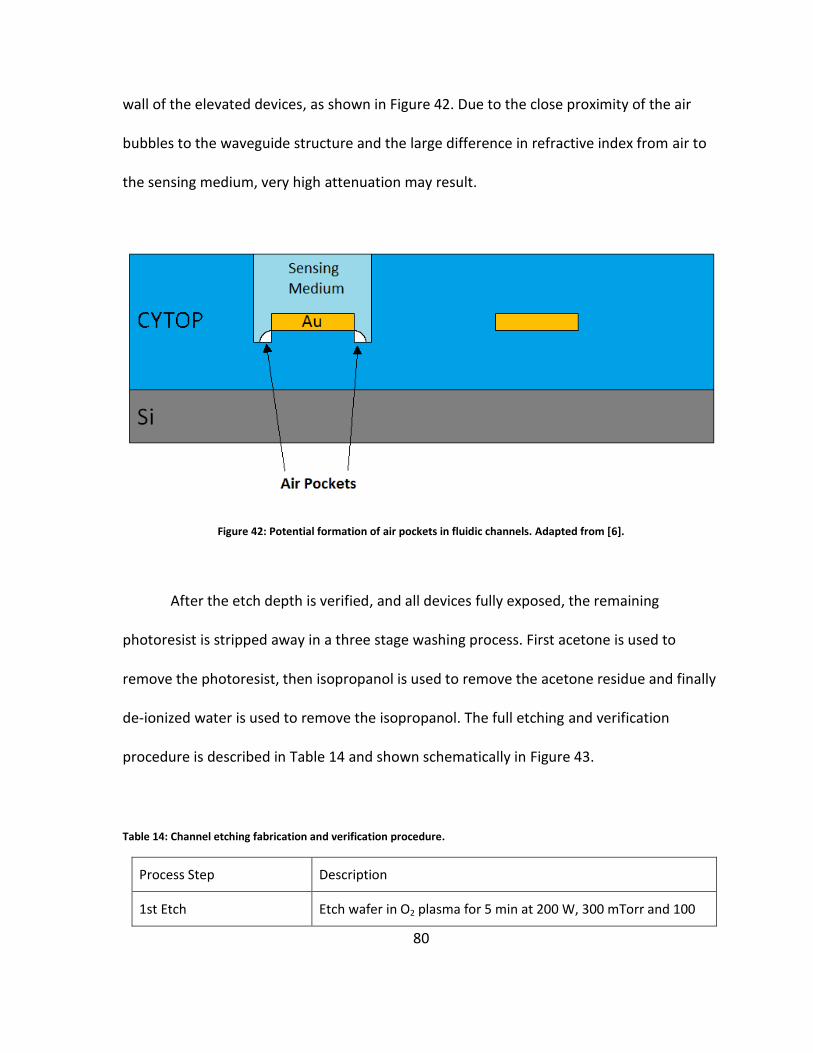
80
wall of the elevated devices, as shown in Figure 42. Due to the close proximity of the air
bubbles to the waveguide structure and the large difference in refractive index from air to
the sensing medium, very high attenuation may result.
Figure 42: Potential formation of air pockets in fluidic channels. Adapted from [6].
After the etch depth is verified, and all devices fully exposed, the remaining
photoresist is stripped away in a three stage washing process. First acetone is used to
remove the photoresist, then isopropanol is used to remove the acetone residue and finally
de-ionized water is used to remove the isopropanol. The full etching and verification
procedure is described in Table 14 and shown schematically in Figure 43.
Table 14: Channel etching fabrication and verification procedure.
Process Step Description
1st Etch Etch wafer in O2 plasma for 5 min at 200 W, 300 mTorr and 100

81
sccm O2
Profilometry Scan Channel depth and waveguide exposure checked with Dektak IIA Profilometer
2nd Etch Etch wafer in O2 plasma for 2 min at 200 W, 300 mTorr and 100 sccm O2
Profilometry Scan Channel depth and waveguide exposure checked with Dektak IIA Profilometer
3rd Etch Etch wafer in O2 plasma for 1 min at 200 W, 300 mTorr and 100 sccm O2
Profilometry Scan Channel depth and waveguide exposure checked with Dektak IIA Profilometer
4th Etch Etch wafer in O2 plasma for 30 seconds at 200 W, 300 mTorr and 100 sccm O2
Profilometry Scan Channel depth and waveguide exposure checked with Dektak IIA Profilometer
5th Etch Etch wafer in O2 plasma for 30 seconds at 200 W, 300 mTorr and 100 sccm O2
Repetition Repeat previous 2 steps as needed until all devices on wafer are fully exposed
Cleaning Wafer cleaned in Acetone/Isopropanol/De-ionized water to remove photoresist and clean channels of etchant residue

82
Figure 43: Process flow diagram for fluidic channel etching.

83
Another aspect of importance is the roughness of the etched CYTOP within the
fluidic channels. Roughness is likely to produce a larger pressure drop as the sensing fluid is
pumped through the channel and to introduce turbulence near the sensing surface which
would influence measured binding kinetics. The former would create difficulties for bonded
devices, discussed in Appendix B, since a higher inlet pressure would be required and may
pose a risk of leakage at the bonded interface.
Figure 44: CYTOP surface roughness: a) etched CYTOP, b) un-etched CYTOP.

84
The degree to which the surface roughness inside the fluidic channels will impact
the device operability will need to be investigated more closely. Furthermore, whether or
not this is a variable which may be manipulated by modifying the etch process still needs to
be determined. The difference in roughness between an etched CYTOP surface and an un-
etched CYTOP surface is shown above in Figure 44 a) and b) respectively. A significant
amount of variation has also been observed between different wafers processed under the
same conditions. In some cases an average surface roughness of 32.2 nm, shown in Figure
45 , more than three times that of the etched surface in Figure 44 a) has been observed.
The cause of this variation is not yet fully understood and warrants closer inspection in
future fabrication runs.
Figure 45: Etched CYTOP surface showing excessive surface roughness.

85
5.4. Device Characterization (Physical)
Once the flow channels are fully etched and the devices have been properly
cleaned, the wafer is coated in a protective film and sent out for dicing. The protective film
used in this case is a thick layer of SPR 220-7, applied in a similar manner to that explained
in Table 12. The photoresist is spun initially at 1000 rpm for 20 seconds followed by 2300
rpm for 30 seconds. Baking of the protective layer is executed in a single step carried out at
105 °C for 3 minutes, because cracking of the photoresist is of little consequence to the
devices; i.e., there is no need for a multi-stage baking process as used in the definition of
the fluidic channels to avoid thermal stress. Care must be taken, however, in ensuring that
the film is cured hard enough such that the photoresist is diced cleanly and not smeared
into the CYTOP at the optical facets (yet soft enough to not chip as the dicing saw cuts
through the wafer). This can be seen in Figure 46 a), in which the diced facet shows signs of
contamination from the photoresist. Conversely, Figure 46 b) shows a diced facet in which
the photoresist was cured properly resulting in a contaminant free facet.

86
Figure 46: Diced facets showing: a) SPR 220-7 contamination on CYTOP, b) clean facet with no signs of contamination.
Once the dies are returned from dicing they are cleaned in a high temperature (80
°C) bath of Microposit 1165 remover, followed by rinsing in isopropanol, and finally dried
under a high purity nitrogen jet. Samples are then selected for AFM scans to check

87
deformation of waveguides, over-etch depth, gold thickness and channel depth. The
remainder of the dies are kept for optical characterization and biosensing experiments.
First discussed is the physical characterization of the devices and fluidic channels,
beginning with the channel and device dimension verification, the most critical of these
aspects being the waveguide width and thickness. The AFM scans, shown below in Figure
47 a) and b), illustrate both the width of the device and the degree of deformation based on
the top cladding formation procedure used. As can be seen, both devices are close to the 5
µm target for width, the main difference being in the level of deformation. Using the new
top cladding process reduces the "bowing" effect of the straight waveguides by a factor of
2.5 times from that seen when using the old top cladding application procedure outlined in
[6]. Furthermore, a substantial reduction in the over etch is noted as a result of more
frequent profilometry checks during the channel etching process. It should also be note that
the extent of solvent ingress beneath the contact pads as a function of the upper cladding
layer showed the process described in [6] was found to be approximately 2.7 times larger
than the modified procedure described within this thesis.
The next dimension to be verified is the thickness of the gold film. In order to
measure the film thickness, a portion of the waveguide was delaminated from the CYTOP
by immersion in an ultrasonic bath. By measuring the difference in height between the top
of the CYTOP pillar and the residual gold surface (schematic shown below in Figure 48), the
gold thickness may be measured. Care must be taken such that the proximity of the

88
measured points is as close as possible to avoid any error which may result due to
waveguide deformation seen above.
Figure 47: AFM scan showing straight waveguide width: a) using new top cladding process, b) using old top cladding process [6].

89
Figure 48: Schematic of gold thickness measurement technique.

90
Figure 49: AFM line profiles for gold thickness verification.

91
Figure 49, above, shows the line profile of a partially delaminated device. The gold
thickness is found to be between 34 and 35 nm, as is expected according to the gold
deposition procedure outlined in Chapter 3.
The final physical dimension that must be measured is the depth of the etched
channel. By subtracting the over-etch depth from this value, an estimate of the cladding
thickness above the waveguides may be obtained. Since a minimum thickness of
approximately 7 µm of dielectric (CYTOP or index matched sensing fluid) is needed both
above and below the device structures, this is a vital measurement for proper device
verification. This measurement may be taken by means of profilometry or AFM, of which
AFM is by far the most accurate. Figure 50, below, shows a line profile taken by AFM,
indicating both the depth of the channel and the shape of the side wall. While the channel
depth is sufficient, there are issues with topographic variations and the shape of the etch
profile, which will hinder the bonding process needed to encapsulate the waveguide and
fluidic channels beneath a glass lid. This is due to the need for the glass wafer to come into
intimate contact with the top of the upper cladding surface, and as such, any imperfections
in the upper cladding surface reduce the overall contact area needed to achieve a sufficient
bond (procedure outlined in Appendix B).

92
Figure 50: Fluidic channel depth showing standard deviation and side wall profile.
5.5. Device Characterization (Optical)
The devices described in this thesis are verified optically by measuring the power
output of waveguides and comparing the experimental values to the expected values,
determined theoretically. The attenuation, or power lost per unit length of the waveguide,
is determined by measuring the total power output for various lengths of waveguides, in
this case 3 mm, 3.8 mm and 4.8 mm long. A plot of power loss as a function of device length
is generated from the results, the slope of which yields the attenuation value in dB/mm
while the y-axis intercept yields the total coupling losses which is subsequently divided by 2
giving the coupling loss per facet (input and output) in dB.

93
Figure 51: Cutback curve comparing devices fabricated with old process and new process to theoretical values. Error bars not accounting for variation in insertion losses
Table 15: Attenuation and coupling loss values of devices compared to theoretical values.
Variable Fabrication Procedure
Theoretical Value Old Fabrication Process New Fabrication Process
Attenuation (dB/mm)
7.2 5.9 ± 0.56
(5.34 to 6.46)
5.6 ± 0.95
(4.59 to 6.51)
Coupling Loss per Facet (dB)
0.89 0.57 ± 0.73
(-0.16 to 1.30)
2.88 ± 0.96
(1.93 to 3.83)
* Deviation values based on 95% confidence interval

94
Figure 51 and Table 15, above, show the results of the optical characterization of
devices fabricated using the new procedure outlined in this thesis versus devices fabricated
using the old procedure outlined in [6] (measurements obtained by Asad Khan, M.A.Sc.
candidate, University of Ottawa and Hui Fan, Ph.D. candidate, Univeristy of Ottawa). Both
sets of data are then compared to theoretical values calculated using COMSOL software [6].
As the above data indicates, both fabrication procedures yield lower attenuation values
than the theoretical model predicted, with the lowest value belonging to the new
fabrication procedure. This is presumably due to the combination of eliminating "spits" on
the gold surface and reducing the overall degree of deformation in the waveguides.
Furthermore, it is believed that the lower than expected attenuation values are a result of
thinning of the waveguides [24] due to the “bowing” effect previously described. Since the
waveguides are of fixed volume and the straight line distance from one edge to the other
remains fixed at 5 µm, the waveguide thickness must decrease in order to accommodate
the change in shape.
The coupling loss per facet for devices fabricated using the new procedure was
observed to be slightly higher than that of the theoretical value; however, this is believed to
be a result of insufficient cleaning prior to testing. Coupling losses are also strongly
dependant on the diced facet quality and alignment of the fiber-optic cable to the
waveguide. These factors, in conjunction with the limited number of tested samples, make
coupling loss measurement highly sensitive to human error and as such would require more
careful testing in order to properly verify the value reported in Table 15. This would also

95
explain the large standard deviation observed in both attenuation and coupling loss
measurements.
After optical characterization, the devices are tested in order to verify biosensing
capability. Two different tests were executed in order to check sensor functionality:
detection of Bovine Serum Albumin (BSA) and selective differentiation of red blood cells
(RBC's) (measurements were obtained by Alex Krupin, Ph.D. candidate, University of
Ottawa).
Figure 52 shows a binding curve of BSA on a 16-MHA self assembled monolayer vs
that of BSA on poly-ethylene glycol (PEG). 16-MHA has a chemical formula of
HSCH2(CH2)13CH2COOH, this enables the thiol end group to bind to the gold surface leaving
the carboxylic acid end group for BSA immobilization, conversely, PEG has a chemical
formula of HOCH2(CH2OCH2)nCH2OH and is a known agent for blocking of protein binding
[23]. After functionalization of the sensor surface is completed, a buffer solution of
phosphate buffered saline (PBS) and glycerol (Gly) is injected into the flow channels at a
rate of 20 µL/min and a concentration of 7.25 wt% glycerol. The precise glycerol
concentration is important in order to closely match the refractive index of CYTOP (PBS/Gly
n=1.3302, CYTOP n = 1.3385). It has been determined experimentally that having the
refractive index of the fluid in the channel slightly below that of CYTOP yields the best
results [7]. This solution is passed through the fluidic channels for several minutes in order
to get a baseline reading of the power output. Once the baseline is determined, a solution
100 µg/mL of BSA in the PBS/Gly buffer is then pumped through the channels at the same

96
flow rate (20 µL/min). As the BSA is immobilized on the waveguide surface (due to the 16-
MHA SAM), a shift in the output power can be observed. As the curve levels off, the fluid
passing through the channel is switched back to the original PBS/Gly buffer solution
triggering a very small decrease in signal power due to a change in the refractive index of
the fluid. Since the signal power does not change appreciably after removing BSA from the
sensing medium, it is evident that successful immobilization of the targeted analyte has
occurred. When compared to a similar binding curve generated with a PEG functionalized
surface (figure 53), the change in power is substantially smaller. Some adsorption is
observed due to the small size of PEG [22], however this is substantially less than that seen
on a 16-MHA functionalized surface, indicating that protein adsorption was successfully
inhibited with the use of PEG on the gold surface.
Figure 52: Binding curve for BSA on 16-MHA vs. PEG. Adapted from [22].

97
Figure 53 shows the application of the fabricated structures in the differentiation of
type A red blood cells (a-RBC's) from type O red blood cells (o-RBC's). In this case, the
purpose of the test was to show selective capture of a specific analyte, namely a-RBC's. The
sensor surface is functionalized with Anti-A-IgG antibodies; this is done first by incubation in
16-MHA for 2 to 24 hours, followed by a 1 hour incubation in a PBS solution containing 1
mg/mL antibodies, a more detailed description of the functionalization procedure is
explained in [7]. Initially the same PBS/Gly buffer solution used in BSA sensing is passed
through the fluidic channels, this time at a rate of 65 µL/min to establish the baseline signal
(inset a). At 7 minutes, the waveguide was exposed to a PBS/Gly buffer solution containing
5 × 10⁷ cells/mL of o-RBC's under static conditions (no flow) for a period of 5 minutes.
During this time, there is a substantial decrease in signal power (inset b) due to settling of
cells on the waveguide surface. Once five minutes have passed, the PBS/Gly buffer solution
is pumped through the channels once again to flush out the o-RBC's and return to the
baseline signal (inset c). The rapid return of the signal power to the baseline indicates that
no binding of the o-RBC's occurred on the Anti-A-IgG functionalized surface. The channels
are flushed with the buffer solution for 9 minutes to ensure all o-RBC's are removed. At the
24 minute mark, a solution of PBS/Gly buffer containing 5 × 10⁷ cells/mL of a-RBC's is
allowed to contact the sensing surface under static conditions for a period of 5 minutes,
again resulting in a substantial decrease of signal strength (inset d). At the end of the five
minutes, the channel is again flushed with PBS/Gly buffer solution, this time the signal
power does not return to the baseline (inset e) indicating successful, selective

98
immobilization of a-RBC's. Flushing of the channel lasts 8 minutes with no change in the
signal power, after which, de-ionized water is pumped in at a rate of 65 µL/min. This
restores the signal strength partially (inset f) as a result of cell rupture but is unable to
return to the baseline power due to a mismatch in the refractive index between water and
CYTOP. Finally, at the 44 minute mark, the channel is again flushed with the PBS/Gly buffer
solution resulting in full restoration of the signal strength (inset g).
Figure 53: Power output graph for differentiation of type O and type A red blood cells. Adapted from [7].

99
6. Conclusions, Contributions and Future Work
The described works are an extension of the research carried out in Chiu et al. 2009
[6]. The contributions made in this thesis include improvement of waveguide feature
definition through material substitution in the bi-layer lithography procedure, elimination
of aberrations and reduction of roughness on waveguide surface through modification of
the gold deposition process and reduction in the degree of deformation of waveguides by
reduction of solvent in the upper cladding through increased baking temperatures.
The combined effect of these three changes led to significantly improved devices
whcih produced a lower background radiation and a reduction in the attenuation values of
the propagating waves. Theoretical values obtained by simulations performed in Daviau et.
al. 2010 [24], yielded an average attenuation value of 7.2 dB/mm for a 5 µm wide, 35 nm
thick gold waveguide embedded in CYTOP. Devices fabricated from the procedure outlined
in Chiu et. al 2009 [6] yielded an average attenuation value of 5.9 dB/mm, compared to an
average attenuation value of 5.55 dB/mm for the devices fabricated using the process
described in this thesis. 95 % confidence intervals were calculated for both sets of devices
and were found to be in the ranges of (5.34 dB/mm to 6.46 dB/mm) and (4.59 dB/mm to
6.51 dB/mm) for the old and new processes respectively. While the average value of the
devices fabricated using the new process is lower than that of those fabricated with the old
process, the values were found to not be statistically different. This is due to the higher
degree of variability of the devices made using the procedure outlined in this thesis. A more
detailed characterization of the devices is required still to be able to indeed conclude that

100
the two procedures produce device of indiscernible quality. This will require testing of
features other than just straight waveguides, such as MZI's and coupler waveguides.
Further testing is required in order to characterize the MZI's as well as a detailed
comparison of the biosensing capability of wafers manufactured under both sets of
processing conditions. It is expected that the new fabrication procedure will produce more
evenly split power modes in the MZI structures and as such yield more consistent and
reproducible results, as of yet, MZI's fabricated under the old procedure have not been able
to be tested.
Further efforts to increase the depth of the fluidic channels as well as encapsulate
the devices are also under way. This will allow for simpler setups when performing optical
characterization and biosensing experiments, as well as allowing for detection of larger
analytes and reduction of the pressure drop through the channels.
In addition to device testing and the bonding work, publications are also underway:
the first being a proceedings paper for research presented during the Photonics North
conference held in Montreal, QC, Canada in June of 2012 entitled "Fabrication of surface
plasmon waveguides in CYTOP". This will focus on the modified fabrication procedure
described in this thesis up to, but not including, the encapsulation process. A second
publication is also underway, aimed at a more reputable fabrication based journal, the title
of the article is still to be determined; however, the focus will be on the incorporation of a
viable encapsulation process which will allow for successful sealing of the fluidic channels.
101
7. References
1. Rogers, K. R. "Recent advances in biosensor techniques for environmental
monitoring", Analytica Chimica Acta, Vol. 568, 222 - 231. (2006)
2. Ruan, C., Zeng, K., Verghese, O. K., Grimes, C. A. "A magnetoelastic bioaffinity-based
sensor for avidin", Biosensors and Bioelectronics, Vol. 19, 1695 - 1701. (2004)
3. Zhang, X., Ju, H., Wang, J. "Electrochemical sensors, biosensors and their biomedical
applications", Elsevier. (2008)
4. Anjanappa, M., Datta, K., Song, T. "The mechatronics handbook", CRC Press. (2002)
5. Kasten, F. H., "Fluorescent and Luminescent prodes for biological activity 2nd Ed.",
Elsevier. (1999)
6. Chiu, C. "Fabrication of surface plasmon waveguide devices in CYTOP with
microfluidic channels", M.A.Sc. Thesis, University of Ottawa. (2009)
7. Krupin, O. "Biosensing using long-range-surface-plasmon-polariton (LRSPP)
waveguides", Ph.D. Thesis Proposal, University of Ottawa. (2011)
8. Love, J. C., Estroff, L. A., Kriebel, J. K., Nuzzo, R. G., Whitesides, G. M. "Self-assembled
monolayers of thiolates on metals as a form of nanotechnology", Chemical Reviews,
Vol. 4 (105), 1103 - 1169. (2005)
9. Maier, S. A. "Plasmonics: fundamentals and applications", Springer. (2007)
10. Chiu, C., Lisicka-Skrzek, E., Tait, R. N., Berini, P. "Fabrication of surface plasmon
waveguides and devices in CYTOP with integrated microfluidic channels", Journal of
Vacuum Science and Technology B, Vol. 28 (4), 729 - 735. (2010)

102
11. Haniff, R. "Microfabrication of plasmonic biosensors in CYTOP integrating a thin SiO2
diffusion and etch-barrier", M.A.Sc. Thesis, University of Ottawa. (2011)
12. Geddes, C. D. "Reviews in plasmonics", Springer. (2010)
13. Herminjard, S., Sirigu, L., Herzig, H. P., Studemann, E. "Surface plasmon resonance
sensor showing enhanced sensitivity for CO2 detection in the mid0infrared range",
Optics Express, Vol. 17, 293 - 303. (2009)
14. Berini, P., Charbonneau, R., Lahoud, N., Mattiussi, G. "Characterization of long-range
surface plasmon polariton waveguides", Journal of Applied Physics, Vol. 98 (1),
043109, 1 - 12. (2005)
15. Berini, P. "Bulk and surface sensitivities of surface plasmon waveguides", New
Journal of Physics, Vol. 10, 1 - 37. (2008)
16. “Amorphous Fluoropolymer CYTOP: Tehcnical Data”, Asahi Glass Company,
http://www.agc.cp.jp
17. "PMGI SF series resists material safety data sheet", Microchem Corporation,
http://www.first.ethz.ch/infrastructure/Chemicals/Ebeam_lithography/MSDS_PMGI
SF8.pdf
18. Jones, S. W. "Photolithography", IC Knowledge LLC. (2008)
19. "Metallization", Carleton University,
http://www.doe.carleton.ca/facilities/fab/metal.php

103
20. "Nano PMGI Resists", Microchem Corporation,
http://www.first.ethz.ch/infrastructure/Chemicals/Ebeam_lithography/Data_PMGI.
21. "PMGI and LOR Resists: FAQ's", Microchem Corporation,
http://www.microchem.com/pmgi-lor_faq.htm
22. Krupin, O., Asiri, H., Wang, C., Tait, R. N., Berinin, P. "Biosensing using straight long-
range surface plasmon waveguides", Optics Express, (Submitted)
23. Beringer, J., Napoli, A., Graf, M., Textor, M., Hubbel, J. "PPS-PEG block copolymers
render hydrophobic surfaces protein and cell resistant", European Cells and
Materials (Suppl. 1), Vol. 2, 45, (2001)
24. Daviau, R., Khan, A., Lisicka-Skrzek, E., Tait, R. N., Berini, P. "Fabrication of surface
plasmon waveguides and integrated components on CYTOP", Microelectronics
Engineering, Vol. 87, 1914 - 1921. (2010)
25. "Surface plasmons", Optrel GBR, http://www.optrel.de/pdfs/flyer/spr-prinzip.pdf
26. Albella, P., Saiz, J. M., Gonzalez, F., Moreno, F. "Surface monitoring based on light
scattering by metal nanosensors", Journal of Quantitative Spectroscopy and
Radiative Transfer, Vol. 112, 2046 - 2058. (2011)
27. Axelrod, D., Koppel, D. E., Schlessinger, J., Elson, E., Webb, W. W. "Mobility
measurement by analysis of flourescence photobleaching recovery kinetics"
Biophysical Journal, Vol. 16, 1055 – 1069. (1976)

104
28. "LOR and PMGI resists", Microchem Corporation,
http://www.microchem.com/pdf/PMGI-Resists-data-sheetV-rhcedit-102206.pdf
29. "How does surface plasmon resonance work?", Bionavis Oy Ltd.,
www.bionavis.com/technology/spr/#kretschmann
30. "Megaposit SPR 220 series photoresist for i-line applications", Rohm and Haas
Electronic Materials,
http://ncnc.engineering.ucdavis.edu/pages/equipment/SPR220_Data_Sheet.pdf
31. Umbrecht, F., Muller, D., Gattiker, F., Boutry, C. M., Neuenshwander, J., Sennhauser,
U., Hierold, C. “Solvent assisted bonding of polymethylmethacrylate:
characterization using response surface methodology” Sensors and Actuators A:
Physical, Vol. 156, 121 – 128, (2009)
32. Tsao, C. W., Hromada, L., Liu, J., Kumar, P., DeVoe, D. L. “Low temperature bonding
of PMMA and COC microfluidic substrates using UV/ozone surface treatment” Lab
on a Chip, Vol. 7, 499 – 505, (2007)
33. Kwei, T. K., Zupko, H. M. “Diffusion in glassy polymers. I” Journal of Polymer Science:
Part A-2, Vol. 7, 867 – 877, (1969)
34. Vesely, D. “Diffusion of liquids in polymers” International Materials Reviews, Vol. 53,
299 – 315, (2008)
35. Frisch, H. L., Wang, T. T., Kwei, T. K. “Diffusion in glassy polymers: II” Journal of
Polymer Science: Part A-2, Vol. 7, 879 – 887, (1969)

105
36. Collins, R. “Mathematical modelling of controlled release from implanted drug-
impregnated monoliths” Pharmaceutical Science and Technology Today, Vol. 1, 269
– 276, (1998)
37. "Nano SU-8 Negative Tone Photoresist Formulations 2 -25", Microchem
Corporation, http://www.microchem.com/pdf/SU8_2-25.pdf
38. Tuomikoski, S., Fransilla, S., "Free-standing SU-8 microfluidic chips by adhesive
bonding and release etching", Sensors and Actuators A, Vol. 120, 408 - 415. (2005)

A
Appendix A - Table of Wafers Processed

B
Appendix B - Wafer Bonding Processes
SU-8 Bonding by Thermal Fusion
Two variations of this process were attempted, both resulting in insufficient contact
between the device wafer and the glass lid wafer as well as plugging of the fluidic channels.
The first method involved the use of SU-8 as an adhesive layer to bond between the etched
device wafer and the glass wafer. A 5 µm thick film of SU-8 was spun onto a clean glass
wafer and baked at 70 °C for 30 minutes. The etched device wafer is simultaneously heated
to the same temperature and pressed onto the SU-8 surface, applying pressure from one
edge of the wafer and working across to the other. The wafers are allowed to rest on the
hotplate at 70 °C, without pressure, for 2 hours after the bond is initiated to allow the SU-8
film to conform to the CYTOP surface. After bonding is complete, the SU-8 film is exposed
to UV light through the glass wafer to initiate cross-linking within the layer.
This method is an adaptation of one described in [38], in which SU-8 is bonded to
SU-8 to form large fluidic channels. The authors had reported that channel plugging was an
issue for channels with depths below 100 µm due to high capillary action. Their solution
was to include sacrificial channels to help with overflow of SU-8 during the bonding process
and reduce filling of device channels. With the incorporation of sacrificial channels, there
was still substantial filling of channels less than 100 µm in depth. The depth of the channels
etched into the devices described in this thesis are limited to only 8 µm and as such were
completely filled with SU-8 when attempting to bond. Furthermore, there were large areas
of the wafer where no bond was initiated at all, forming voids, due to the limited thickness
C
of the adhesion layer as well as surface variations present on both the SU-8 and CYTOP. It is
possible to increase the thickness of the adhesion layer; however, this would only result in
further plugging of the fluidic channels and was not investigated further.
The second method involves spin coating SU-8 over the device wafer before channel
definition and performing a flood exposure to fully cross-link the layer. Following the SU-8
application, a thin layer of aluminum is deposited on top of the SU-8 to act as a hard mask
during etching of the fluidic channels. Aluminum is chosen because it is cheap, abundant
and can be selectively removed by MF 321 developer solution. Aluminum deposition is
performed in a similar manner to the gold deposition procedure described in section 0,
except the thickness is set to 100 nm and the maximum e-beam power is set to 35% giving
a deposition rate of ~5 Å/s. A 100 nm thick aluminum film is opaque making channel
alignment to the devices impossible. For this reason two thin strips of tape are placed at the
top and bottom of the wafer prior to aluminum deposition. Once the wafer is removed
from the evaporator chamber, the tape is removed, exposing alignment marks for channel
definition. S1805 photoresist is then spun onto the aluminum in the same manner
explained in the same manner described in Table 5 and exposed using the fluidic channel
mask for 7 seconds in the Karl Suss MA6 mask aligner. Following exposure, the wafer is
immersed in MF 321 for 4 minutes with medium agitation; this selectively removes the
exposed portions of the S1805 and, with it, the aluminum underneath. The wafer is then
etched in O2 plasma; the portions still covered in aluminum remain unaffected while the
developed regions are opened up, eventually making their way down to the device level,

D
exposing the gold surface. The remaining aluminum is then stripped away by immersion in
MF 321 leaving the upper SU-8 surface in its original condition. The SU-8 layer increases the
channel depth by as much as 20 µm. However, when bonding with a glass wafer coated
with a thin film of SU-8 is attempted, similar issues occured as with the previously described
method: large void areas were plainly visible and plugging of channels was still observed in
areas where a bond was initiated. Furthermore, SU-8 has a very high surface roughness
after being etched in O2 plasma (as much as 300 nm) and it was found that this etch profile
transferred through to the CYTOP due to the anisotropic nature of the March Systems
Jupiter II etcher.

E
Appendix C: CYTOP/CTSOLV 180 Diffusion Characterization
Due to the large impact of diffusion of CTSOLV 180 into CYTOP on the quality of the
waveguides during spin coating of the upper cladding, diffusion characterization was
performed in an attempt to better understand the phenomena and manipulate the
processing conditions to improve device quality. The testing consisted of pouring a small
amount of CYTOP (CTX-809SP2) onto a glass wafer and measuring the change in weight as a
function of time at various baking temperatures (50 °C, 75 °C and 100 °C).
The data was plotted as Mi/M∞ versus time, where Mi is the mass of the sample at
some time i and M∞ is the mass of the sample if the test were to run for an infinite period of
time (effectively the mass of solids in the sample after all the solvent has diffused out) [33].
The data was then analysed to determine the type of diffusion (Fickian, Case II or
anomalous) [34]. In Fickian diffusion Mi/M∞ is directly proportional to the square root of
time (t0.5), in Case II diffusion Mi/M∞ is directly proportional to time (t) and anomalous
diffusion is considered to be a combination of the two (t0.5>x>1). In order to determine the
type of diffusion occurring for CTSOLV 180 in CYTOP, Mi/M∞ was plotted against time using
various exponents ranging from 0.5 to 1 in increments of 0.1 (following Equation (1)). Figure
A1 shows linear trend lines fitted to mass data obtained from diffusion testing at 50 °C, it
can be clearly seen that the linear plot is best suited to Mi/M∞ = k t0.5 , where k was found
to be 0.0035.
(1)
[35]
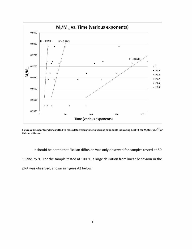
F
Figure A 1: Linear trend lines fitted to mass data versus time to various exponents indicating best fit for Mi/M∞ vs. t0.5
or Fickian diffusion.
It should be noted that Fickian diffusion was only observed for samples tested at 50
°C and 75 °C. For the sample tested at 100 °C, a large deviation from linear behaviour in the
plot was observed, shown in Figure A2 below.

G
Figure A 2: Mi/M∞ vs. t0.5
at various temperatures, showing deviation from Fickian behaviour at 100 °C.
When attempting to fit the mass data for the test performed at 100 °C to an
exponent that would be indicative of either anomalous or Case II diffusion, the deviation
from linearity was only amplified. This would indicate that some other, unexplained
phenomena is occurring to obscure the diffusion profile, complicating the determination of
the exact mechanism of diffusion. Further testing and more detailed analysis of this
phenomenon would be required in order to verify the above findings. The diffusion
coefficients listed below for the sample tested at 100 °C assume the validity of Fickian

H
diffusion although they are subject to uncertainty due to the deviation from the expected
mass profile behaviour.
For Fickian diffusion, the primary equation of interest is:
(2)
[34]
Where, D = Diffusion coefficient (cm2/s) k = Slope of the curve following (Mi/M∞ vs. t0.5) L = Characteristic length of diffusion (thickness of CYTOP film in this case)
Table A1 below indicates diffusion coefficients of CTSOLV – 180 through CYTOP as a
rubbery solid as well as those determined for CYTOP as a glassy solid. This was done by
separating the diffusion curve into three sections: (1) the viscous liquid stage, typically
lasted less than a few minutes at 50 °C, decreasing in duration with increasing
temperature. (2) the rubbery solid stage, lasting anywhere from 30 minutes at 100 °C to
as much as 3 hours at 50 °C. (3) glassy solid, final stage of diffusion, beyond this region
change in mass was very small over large periods of time due to minimal void volume
between polymer chains. Solvent mobility is greatly hindered and for all practical
purposes, solvent removal rate is effectively zero.
Table A 1: Diffusion coefficient summary table for rubbery and glassy solids at various temperatures.
Temperature (°C) 50 75 100
Diffusion Coefficient (cm2/s)
Rubbery Solid 2.45 × 10⁻¹⁶ 4.40 × 10⁻¹⁶ 6.11 × 10⁻¹³
Glassy Solid 8.32 × 10⁻¹⁸ 6.06 × 10⁻¹⁷ 3.69 × 10⁻¹⁵

I
It should be noted that the diffusion rates for the viscous liquid stage were not
reported due to the inability for accurate measurement and determination of convective
diffusion rates as well as the very short time that CYTOP spends as a viscous liquid, even at
low temperatures. Figure A3, shown below, illustrates the mass of a sample as a function of
time throughout the baking procedure for temperatures of 50 °C and 100 °C. As can be
seen, there is a substantially rapid decrease in mass very early in the baking process (more
pronounced in 100 °C sample), indicating the short period of time the sample spends in the
liquid phase. The curve in the profile indicates the rubbery solid region, which for practical
application is the phase that will be of most interest when applying the upper CYTOP
cladding. As the profile levels off, the sample becomes glassy and any change in mass is
minimal, requiring long baking periods to achieve minimal amounts of solvent removal.

J
Figure A 3: Mass profiles of baked samples as a function of time. Mi is mass of sample at time i, Mo is mass of sample at time t=0.
Finally it should be noted that a majority of solvent ingression will occur when the
sample is in the liquid phase. Since CYTOP must be baked at a relatively low temperature
initially to avoid bubbling and surface damage due to rapid solvent escape, it will likely be
impossible to completely eliminate device deformation during the upper cladding
deposition process, however, by minimizing the amount of solvent in the upper cladding
layer closest to the devices, and subsequent layers thereafter, the CYTOP can be
maintained as a glassy solid thus minimizing the amount of deformation occurring.
As of yet, the optimal conditions appear to be those described in Chapter 4, in which
each upper cladding layer is baked at 100 °C to drive off a maximum amount of solvent and
shift the CYTOP into the glassy state. Then by depositing the subsequent layer and baking at

K
50 °C, it is possible to exploit the best of both tested properties; the reduced diffusion
coefficient due to its dependence on temperature, as well as the reduced diffusion
coefficient due to its dependence on the state of the material it is diffusing through.