fabrication of textured surface solar …arizona.openrepository.com/arizona/bitstream/10150/... ·...
TRANSCRIPT

Fabrication of textured surface solarcells with the help of anisotropic etching
Item Type text; Thesis-Reproduction (electronic)
Authors Dixit, Suresh Gopal, 1946-
Publisher The University of Arizona.
Rights Copyright © is held by the author. Digital access to this materialis made possible by the University Libraries, University of Arizona.Further transmission, reproduction or presentation (such aspublic display or performance) of protected items is prohibitedexcept with permission of the author.
Download date 13/06/2018 23:43:30
Link to Item http://hdl.handle.net/10150/348135

FABRICATION OF TEXTURED SURFACE SOLAR CELLS WITH THE HELP OF ANISOTROPIC ETCHING
Suresh Gopal Dixit
A Thesis Submitted to the Faculty of theDEPARTMENT OF ELECTRICAL ENGINEERING
In Partial Fulfillment of the Requirements . For the Degree ofMASTER OF SCIENCE
In the Graduate CollegeTHE UNIVERSITY OF ARIZONA
1 9 7 7

STATEMENT BY AUTHOR
This thesis has been submitted in partial fulfillment of requirements for an advanced degree at The University of Arizona and is deposited in the University Library to be made available to borrowers under rules of the Library.
Brief quotations from this thesis are allowable without special permission, provided that accurate acknowledgment of source is made. Requests for permission for extended quotation from or reproduction of this manuscript in whole or in part may be granted by the head of the major department or the Dean of the Graduate College when in his judgmentthe proposed use of the material is in the interests of scholarship. Inall other instances, however, permission must be obtained from the author.
SIGNED:
APPROVAL BY THESIS DIRECTOR
This thesis has been approved on the date shown below:
S AufoZC 1977v R. L. CALL " ^ /Date
Professor of Electrical Engineering .

ACKNOWLEDGMENTS
The author wishes to thank Dr, Reginald L. Call for his guidance
and encouragement in writing this thesis; also. Dr. Roger C. Jones for
his critical comments•The author gratefully acknowledges Miss Candice R, Corley for her
careful typing of the manuscript.

TABLE OF CONTENTS
PageLIST OF ILLUSTRATIONS . . . . . . . . . . . . . . . . . . . . .. v
LIST OF TABLES . . . . . . . . . . . . . . . . . . . . . . . . . viABSTRACT ........ . . vii
1. INTRODUCTION . . . . . . . . . . . . ........ . . . . . . . . . 1
2. ETCHING ................ 4
Basic Mechanism of Etching .............. 4Etching Processes . . . . . . . . . . . . . . . .......... 6
Chemical Etching . . . . . . . . . . . . . . . . . . . 6Vapor Etching . . . . . . . . . . . ........ . . . . 7
Etch Rate 7
3. ANISOTROPIC E T C H I N G . ............... 10
Experimental.Procedure . . . . . . . . . . . . 10Details of Experiments . . . . . ................ 12Conclusions . . , . ............ 16
4. TEXTURED SURFACE SOLAR CELLS ........ 18
Spectral Response of a Solar Cell . . . . . . . . . . . . . 18Fabrication Technique of Textured Surface Solar Cells .. . 211-V Characteristics . . . . . . . . . . . . . . . 21Series and Shunt Resistance of the Solar Cell . . . . . . . 26
REFERENCES . . . . . . . . . . . . . . . . . . . . . . . . . . . 28
iv

LIST OF ILLUSTRATIONS
Figure Page1.1 . Reflection Phenomenon for Textured Surface .......... 2
2.1 Etch Rate (re) against Etchant Temperature (T) for aComposition KOH/H 0 = 1/2; <100> Silicon . . . . . . . . 9
3.1 Intersecting <111> Planes Exposed after SelectiveEtching of <TOO> Silicon . . . . . . . . . . . . . . . . . 11
3.2 Results of Etching <100> Silicon in Etches ContainingPotassium Hydroxide, 2-Ethoxyr-Ethanol and DeionizedWater; 320X Magnification . .............. . . . . . . 13
4.1 Electrical Equivalent of a p-n Junction Exposed to Light . . 194.2 Junction Formation on p-Type Textured Silicon by Diffusion . 22
4.3 I-V Characteristics of Standard Solar Cell . . . . . . . . . 24
4.4 I-V Characteristics of Textured Surface Solar Cell ......... 25
4.5 Equivalent Circuit of a Solar Cell . . . . . . . . . . . . . 27
v

LIST OF TABLES
Table Page4.1 Short-Circuit Currents and Open-Circuit Voltages for
Standard and Textured Surface Solar Cells . . . . . , . . 23
vi

ABSTRACT
Textured surface solar cells have a higher conversion efficiency
than flat surface solar cells. There are many possible ways of producing texture on a wafer of single crystal silicon. Anisotropic chemical etching is the best way to obtain the desired texture. An etch con
taining potassium hydroxide, deionized water, and 2-ethoxy ethanol was
perfected after conducting various experiments on <100> silicon. Solar
cells were fabricated from the etched silicon using standard production
methods. On the basis of the results obtained, it is concluded that,
although the textured surface solar ceils have a higher conversion efficiency, they suffer from a low shunt resistance. It is further concluded
that the shunt resistance can be increased by using silicon having a very small number of surface and crystallographic defects.

V
CHAPTER 1
INTRODUCTION
Solar cells have been in use for the last twenty-five years as a
means to convert radiation of sun in optical spectrum into useful elec
tric power. In solar cells, this takes place by the photovoltaic principle.
Basically, a solar cell is a p-n junction with a large surface area. The junction depth is kept as low as possible so that the loss of
optically generated holes and electrons due to recombination would be
minimum.A solar cell with a polished, flat surface absorbs approximately
75% of the incident light. The remaining 25% is reflected back into the
atmosphere. If the amount of light reflected back can be reduced, the
solar cell would be absorbing more light and the photovoltaic conversion
would occur at a better efficiency. One way of doing this is to coat the
surface of the cell with an antiref1ective material like Silicon monoxide.
The conversion efficiency of a flat-surface solar cell with antireflec- tive coating is about 12.5% to 13%.
To increase the efficiency still_further, a textured surface is used instead of a flat surface. Typically, a textured silicon surface
hns a large number of tiny pyramids formed by anisotropic etching.
Figure 1.1 shows the reflection phenomenon for the textured surface. The
geometry of the pyramids is such that the first reflection of light is
. 1
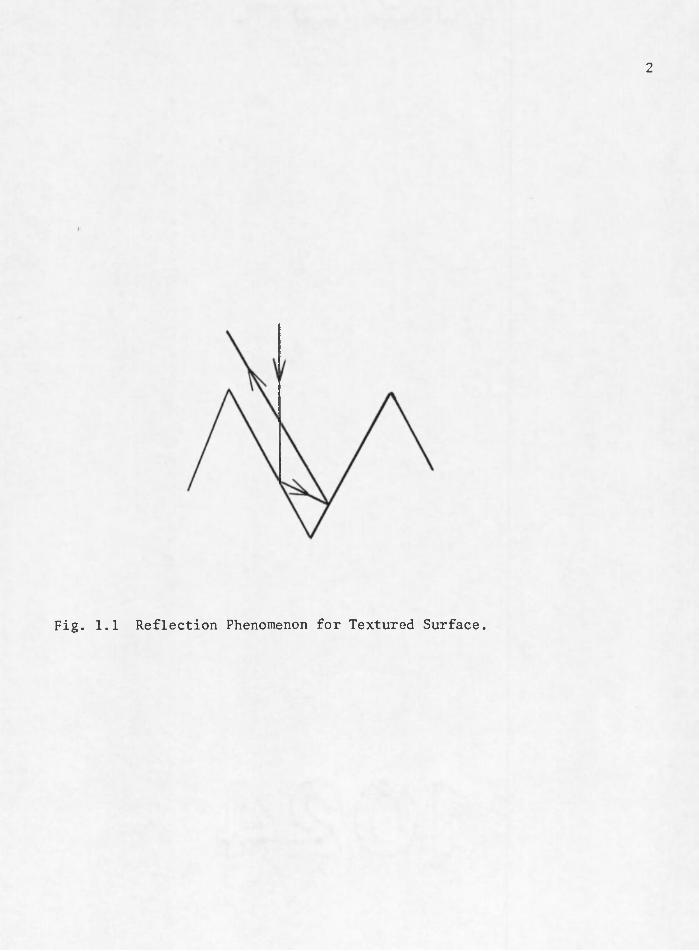
2
Fig. 1.1 Reflection Phenomenon for Textured Surface.

3absorbed by the walls of the adjacent pyramids, instead of being lost
back into the atmosphere. This class of solar cells is called textured surface solar cells.
There are various ways of producing the desired texture on a
silicon surface. Most of the chemical etches currently in use are far
from being perfect. In the coming years, we can expect a better under
standing and control of the etching process, leading to solar cells with
conversion efficiency close to 20%.

CHAPTER 2
ETCHING
Basic Mechanism of Etching
Chemical etching of a seMconductor surface is the result of the
dissolution of the semiconductor in an oxidizing electrolyte solution.
The nature of the semiconductor, the presence or absence of lattice
defects, crystal orientation, type and concentration of impurity atoms, and the flow of the etchant solution over the semiconductor surface are
the factors that determine the etching process.
In an elemental semiconductor, the dissolution process involves
the oxidation of the semiconductor from its zero oxidation state to a higher state which is either soluble in the electrolyte or forms
insoluble products away from the surface. In a compound semiconductor, the same conditions apply but several oxidation reactions may occur
simultaneously.
There are two steps involved in the chemical etching of a semi
conductor. The first is oxidation-reduction. The second is the dissolu
tion of oxidation products in the form of complex soluble ions. The
oxidation occurs through an anodic reaction while the reduction occurs
through a cathodic reaction. Corrosion currents of sufficient magnitude
due to anodic and cathodic reactions lead to the actual etching. Uniform
etching is the result of both the reactions taking place over
4

approximately equal amounts of time. Selective etching occurs if anodic
and cathodic reactions take place over widely differing times on different parts of the silicon surface (Wolf, 1971).
In an anodic reaction, oxidation takes place along with a loss of
electrons. In a cathodic reaction, reduction occurs with a gain of electrons. . The loss and gain of electrons can be viewed as localized
corrosion currents. The overall balance between anodic and cathodic
reactions is such that the net exchange of electrons is zero.
Oxidation of pure silicon can occur by the following electrochemical reactions in an alkaline solution:
Si + 2H20 Si02 + 4H+ + 4e (1)
Si + 60H™ Si032* + 3H20 + 4e (2)
The hydroxyl ions are created through the breaking of the bond in
potassium hydroxide. Further, potassium monosilicate which is soluble in
water is formed by the following reaction:
2K+ + Si032' ^ K2Si03 (3)
In a cathodic reaction, reduction of silicon takes place and
hydrogen is evolved. First, silicon hydride is formed on the surface by
the following electrochemical reaction:
Si + e (valance band) + H -> SiH (chemical bond) (4)

Evolution of hydrogen occurs after the capture of a free elec
tron. This reaction takes place in the following manner:
SiH + e + H+ Si + H2 (5)
The degree of selectivity and the rate of■etching are governed by
crystallographic orientation, surface and bulk defects, composition of
the etch, temperature, and the hydrodynamics of the semiconductor-etchant
interface. The etching process is either reaction-rate-limited or
diffusion^limited. This means that the etch rate is either a function of the reaction rate or of how fast the etchant can diffuse through a sur
face layer. In general, etchant movement enhances the etch rate and also
prevents the generation of localized temperature rise.
Etching Processes
Semiconductor etching falls into two types: chemical etching and
vapor etching.
Chemical Etching
Most chemical etches contain hydrofluoric acid (HF) as the
complexing agent and nitric acid (HNO^) as the oxidizing agent. Some
etches act preferentially, others nonpreferentially. However, some
etches can act both ways depending upon relative HF/HNO^ proportions,
temperature, and other conditions. Nonpreferential (isotropic) etches
are used to eliminate surface contaminations, to remove work-damaged
material, and to control thickness. Preferential (anisotropic) etches

are used to determine crystal orientation, to expose crystal imperfections, and to facilitate dielectric component isolation.
Vapor Etching
This is a high-temperature process and usually involves the oxida
tion or another conversion of a surface layer into a silicon compound and
its subsequent removal. It avoids contamination of the surface by the
reagents employed in chemical etches. It is used to expose a fresh
silicon surface immediately prior to metal evaporation or deposition of an epitaxial layer.
Etch Rate
If surface reaction limits the etch process, then the etch reac
tion is reaction-rate-limited. On the other hand, if the transport of
etchant and reaction products to and from the surface limits the etch
process, then the etch reaction is diffusion-limited. The following
factors control the rate of etching*
1. Temperature: The surface reaction rate depends exponentially on
temperature. Hence, a rapid etchant movement prevents localized
. temperature increases and gives more uniform etching results.
2. Surface damage: A damaged surface can mean larger effective sur
face area exposed to the etchant. This leads to an increased
rate of etching.
3. Surface films: If insoluble reaction products occur, they pro-
. duce surface films. Surface films reduce the etch rate.

4. Crystal defects: Usually, defects are related to the segregationof impurities and can lead to an increased rate of etching in their vicinity.
5. Impurities in the etchant: These impurities affect the absorp
tion processes of the semiconductor surface. Therefore,
depending upon the nature of the impurities, the rate of etching
may increase or decrease.
Anisotropic etching means the preferential etching along a cer
tain crystallographic plane. Most etches used for preferential etching of <100> silicon contain potassium hydroxide (KQH) or sodium hydroxide
(NaOH). The anisotropic etch rate is significantly lower than the
isotropic etch rate. Figure 2.1 shows the dependence of the rate of
etching on etchant temperature for a certain composition of the etchant.
The curve depicted is for <10,0 silicon (Wolf, 1971).

UTUI/Ulrt
9
10
1
110
210
3100 50 100
T, °C
Fig, 2,1 Etch Rate (re) against Etchant Temperature (T) for a Composition KOH/HgO = 1/2; <100> Silicon.

CHAPTER 3
ANISOTROPIC ETCHING
In the fabrication of solar cells, anisotropic etching is used to
produce a textured surface which has low reflection loss of the incident
light. In the original concept of reducing silicon reflectivity by
physically altering the geometry of the silicon surface, ultrasonic
cutting was employed to produce numerous inverted tetrahedra on the
silicon surface (Dale and Rudenberg, 1960).
Preferential chemical etches on <100> orientation silicon sur
faces can selectively expose <111> planes which intersect the surface
with four-fold symmetry and form an angle of 54.7° between them as shown
in Fig. 3.1. This geometry is helpful in preparing a low reflection sur
face because incident light undergoes two reflections prior to escape.
The crystal1ography of the silicon determines the geometry and angles of
these structures (Lee, 1969).
Experimental Procedure
There are several anisotropic etches that may be used for pro
ducing a textured silicon surface. The etch containing hydrazine was not
used in any of the experiments conducted because of the fact that hydra
zine is a highly explosive chemical and requires special apparatus to
ensure safety. Further, the etch also requires oxide and photoresist
masking to produce the desired results (Baraona and Brandhorst, 1975).
■

11
original <100> plane
<111> plane <111> plane
Fig. 3.1 Intersecting <111> Planes Exposed after Selective Etching of <100> Silicon.

12The etch containing only potassium hydroxide (BOOH) also requires
oxide and photoresist masking to produce a textured surface. In the
absence of such masking, the etch yields a shiny surface with numerous
square, shallow depressions rather than a textured surface. The diffi
culties involved in preparing photomasks of microscopic dimensions can be
avoided by using an etch which contains a 2-mole solution of potassium hydroxide (KOH), 2-ethoxy-ethanol, and deionized water of high purity.
Presence of 2-ethoxy-ethanol makes the hydroxide more reactive and
orients the oxygen atoms properly to form the bond with silicon atoms. Various etching experiments involving different amounts of these three
elements were carried out. The time involved and the operating tempera
ture were varied in an effort to obtain reproducible etching results.
These experiments are described below along with magnified photographs of
the five most important resulting surfaces. The photographs appearing in
Fig. 3.2 have 320X magnification.
Details of Experiments
Experiment No. 1: An etch containing 40 cc each of potassium
hydroxide 2-mole solution, 2-ethoxy-ethanol, and deionized water was used2
for etching a silicon wafer of 4 cm area. The temperature of the etch
was allowed to rise from 30°C to 90°C in 50 minutes. This etch yields a
shallow, grainy texture on the wafer surface which has a dull appearance
(see Fig. 3.2a).
Experiment No. 2: An etch containing 60 cc each of potassium
hydroxide 2-mole solution and 2-ethoxy-ethanol was tried on a silicon
wafer of 4 cm area. Etching was performed for 35 minutes during which

Fig. 3.,2 Results of Etching <100> Silicon in Etches ContainingPotassium Hydroxide, 2-Ethoxy-Ethanol and Deionized Water;320X Magnification.(a) 40 cc each of potassium hydroxide 2-mole solution,
2-ethoxy-ethanol, and deionized water. Rise in temperature, 30oC to 90°C in 50 minutes; silicon area, 4 cm^.
(b) 60 cc each of potassium hydroxide 2-mole solution and2-ethoxy-ethanol. Rise in temperature, 30°C to 86°C in 35 minutes; silicon area, 4 cm2.
(c) 60 cc each of potassium hydroxide 2-mole solution and2-ethoxy-ethanol. Rise in temperature, 80°C to 95°C in 7 minutes; silicon area, 7.5 cm^.
(d) 50 cc each of potassium hydroxide 2-mole solution and2-ethoxy-ethanol, and 20 cc deionized water. Rise in temperature, 30°C to 86°C in 20 minutes; silicon area, 22.3 cm2.
(e) 50 cc each of potassium hydroxide 2-mole solution and2-ethoxy-ethanol, and 20 cc of deionized water. Temperature rise, 30°C to 90°C in 45 minutes; silicon area, 13 cm2.

*6 1 * WKjO., • i ^fcE ,eicVs.er
(c) (d)
(e)Fig. 3.2 Results of Etching <100> Silicon in Etches Containing Potassium
Hydroxide, 2-Ethoxy-Ethanol and Deionized Water; 320X Magnification.

14the temperature of the etch rose from 30°C to 86°C. This etch produces
shallow pyramid formations on the wafer surface. However, as can be seen from Fig. 3.2b, the distribution density of the pyramids is quite low.
Further, as a result of overetching, the tops of the pyramids became flat)
and high reflective areas. The surface between the pyramids is also very shiny.
Experiment No. .3: In this experiment, the same etch composition
as in Experiment No. 2 was tried. However, the etch temperature was2initially raised to 80°C and then a silicon wafer of 7.5 cm area was
exposed to the action of the etch for 7 minutes during which the tempera
ture increased to 95°C. Figure 3.2c shows the result of this experiment.
Very shallow pyramids appear on the surface. The distribution density of
the pyramids is higher than that obtained in Experiment No. 2, because of
the reduced time allowed for etching. However, some overetching causes
the pyramid tops to become flat and acquire a polished and reflective
appearance.Experiment No. 4 : The etch used for this experiment had 50 cc
each of potassium hydroxide 2-mole solution and 2-ethoxy-ethanol, and220 cc of deionized water. A total silicon surface area of 22.3 cm was
etched for 20 minutes during which the temperature of the etch increased
from 30°C to 860C. The results of this experiment are shown in Fig. 3.2d.
The pyramids that appear on the surface are extremely shallow with their
tops flattened because of overetching. However, the pyramid density is
even higher than that obtained in Experiment No. 3. Because of high
reflectivity of the pyramid tops, the intensity of the incident light had

15to be reduced significantly so that an acceptable photograph could beproduced. This is the reason why Fig. 3.2d looks darker than the rest.
Experiment No. 5: In this experiment, the composition of the
etch was kept the same as in Experiment No. 4. However, an effective2silicon surface area of 13 cm was etched for 45 minutes and the tempera
ture was allowed to rise from 30°C to 90°C during that time. Figure 5.2e
shows the results obtained in this experiment. Pyramids of high uniform distribution density appear on the silicon surface. As a result of
slight overetching, some flattening of pyramid tops occurs. Also, a few
randomly distributed, microscopic regions acquire high reflectivity.
However, the general appearance of the etched wafer is dark as a result
of very little light being reflected back. Also, unlike results from
other experiments, the final texture of the surface is quite deep.
Typical separation between adjacent pyramid peaks is 3 pm and the height
of pyramids is about 7 pm. This gives an angle of approximately 25°
between the adjacent walls of any two pyramids.This experiment was repeated many times to confirm the repro
ducibility of the results obtained in the first trial. After that, the
etch was used in the fabrication of textured surface silicon solar cells.
Several other experiments were also conducted. These did not
yield satisfactory results. However, they helped gain important informa
tion about the roles played by such factors as time, temperature, and
surface conditions of the silicon wafer in the overall etching process.

16Conclusions
On the basis of the experimental work, it is concluded that, at
any given instant, the etching rate is exponentially dependent on the
temperature of the etch. For a given etch composition and temperature,
there appears to be an optimum time of etching to achieve maximum struc
tural perfection and uniformity. If etching continues beyond this time, the pyramids begin to disappear and flat, shiny regions begin to appear.
The results of etching are highly dependent on the composition of
the etch. Excessive amounts of potassium hydroxide in the etch yield
square, shallow depressions on the silicon surface rather than pyramids.
On the other hand, very small amounts of potassium hydroxide in the etch
give only a dull appearance to the surface and no texture at all. Also,
a certain ratio of exposed silicon surface area to total volume of the
etchant has to be maintained to achieve reproducible results. This ratio2has been found to be 13 cm of silicon surface area to 120 cc of the
etchant.
Time and temperature are equally important factors in the etching
process. If etching is performed under constant temperature conditions,
the resultant texture is of poor quality. A1lowing the temperature to rise from a minimum of 30°C to a maximum of 90°C in a short time also
produces unacceptable results. The temperature must be increased at such
a rate that in 45 minutes it will reach the maximum of 90°C.Further, surface conditions are Of critical importance. A saw
cut or lapped starting surface yields more uniformly textured surface
than a chemically or mechanically polished starting surface. Before

17etching, the silicon wafer surface must be thoroughly cleaned by the
'standard laboratory methods. It has been found that oxide films
developed on the surface during the cleaning of the wafer in hot sulphuric acid (H^SO^) prevent the etch from acting on the surface. Such
oxide films must be removed immediately prior to etching with the help of hydrofluoric acid (HF).

CHAPTER 4
TEXTURED SURFACE SOLAR CELLS
The main advantage of textured surface solar cells over conven
tional solar cells is that the loss of incident light due to reflection
back into the atmosphere is significantly reduced. Because of larger amounts of light absorbed by the solar cell, the constant current due to the incident light also increases. A flat surface silicon solar cell
without an antireflective coating has a 25% loss of incident light due to
reflection. An antireflective coating of silicon monoxide reduces the
reflection loss to 10%. Silicon monoxide produces an optical match
between the refractive indices of air and silicon for blue light. The
reflection loss for a textured surface solar cell with an antireflective
coating is only 3%. This leads to the absorption of 97% of the incident
light by the cell and, hence, a larger value of optically generated
current.
Spectral Response of a Solar Cell
The spectral response of a solar cell is defined as the short-
circuit current as a function of the wavelength of the incident light.
Figure 4.1 shows the electrical equivalent of a p-n junction exposed to
light. It is assumed that the depletion'width of the junction is very
much less than L^ and L^, which are the minority diffusion lengths on the
p and n sides, respectively.
18

19
SurfaceJunction
x=0 x=d
Fig. 4.1 Electrical Equivalent of a p-n Junction Exposed to Light.
d, junction depth; Lp, minority diffusion length in n side; Ln , minority diffusion length in p side.

20For incident photons with energies in excess of the energy gap
(hv > E ), the density of photons in the semiconductor is given by:
<f> = <P0 e~ax (6)
2where <f> is the number of photons incident per second per cm and a is the
absorption coefficient of the semiconductor, a is a function of the wavelength of light.
The rate of hole-eleetron pair generation due to photons is given
by:
G(x) = <j>oae~aX (7)
In the n side^ the minority carriers (holes) created at a distance
x will have a fraction proportional to e ~ ^ x^^p diffuse to the junction.
The total number of minority carriers reaching the junction due
to the creation of hole-electron pairs in the n side is given by:
N = / * e " ™ e ' ( d "X :i/L p dxn 0 0
rc"d/Lr - e-"<] (S,a - —
lp
Similarly, the number of minority carriers (electrons) reaching
the junction as a result of the creation of hole-electron pairs in the
p side is given by:
21
^o016'0̂N = I C9)y a + — n
Thus, the total number of carriers crossing the p-n junction is given by:
nt . i v [»"d/Lp - ^ CIO,a - 7— a + ■=—S n
The steady-state current through the cell is proportional to N^. The
energy of individual photons is inversely proportional to the wavelength.
Thus, the solar cell current is a function of the wavelength of the
incident light (Sze, 1969).
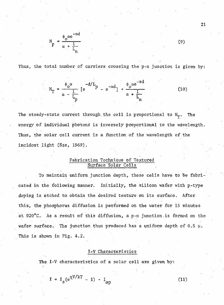
Fabrication Technique of Textured Surface Solar Cells
To maintain uniform junction depth, these cells have to be fabri
cated in the following manner. Initially, the silicon wafer with p-type
doping is etched to obtain the desired texture on its surface. After
this, the phosphorus diffusion is performed on the water for 15 minutes
at 920°C. As a result of this diffusion, a p-n junction.is formed on the
wafer surface. The junction thus produced has a uniform depth of 0.5 y.
This is shown in Fig. 4.2.
I-V Characteristics
The I-V characteristics of a solar cell are given by:
I = isCe^ - _ !) _ iop (ID

22
Fig. 4.2 Junction Formation on p-Type Textured Silicon by Diffusion,
d, the junction depth = 0.5 y.

23where I is the strength of the constant current due to the incident light, and I is the saturation current. From equation (11), we can obtain an expression for the open-circuit voltage as:
XVoc = Vx ' f - ’>'• f if + 0 fl2)
Thus, the open-circuit voltage will be higher for a cell having a higher
current generated by incident light.
The characteristics of a textured surface solar cell and a
standard cell for one sun intensity of light are shown in Fig. 4,3 and
Fig. 4.4, respectively. Both cells were fabricated from 10 ohm-cm single2crystal silicon. However, the standard cell has a surface area of 4 cm ,
whereas the textured surface solar cell has an active surface area of 22.9 cm , The results for the two cells are shown in Table 4.1.
Table 4,1 Short-Circuit Currents and Open-CircuitVoltages for Standard and Textured Surface Solar Cells.
Cell Type V v ™ 2
Standard
Textured surface
0.55 V
0.5774 V
35 ma
42 ma
2If the textured surface solar cell had an area of 4 cm , it would have
produced a short-circuit current of 168 ma.

24
sc140
oc0.2
V, volts
Fig. 4.3 I-V Characteristics of Standard Solar Cell.
Cell surface area = 4 cm^; Isc = 140 ma, V0e = 0.5447 volts.

25
sc
mp
mp
V, volts
Fig. 4,4 I-V Characteristics of Textured Surface Solar Cell.
Cell surface area = 2.9 cirr; lgc = 122 ma; Voe - 0.5774 volts; ■’••rap - 95 ma; = 0.4985 volts.

26Series and Shunt Resistance of the Solar Cell
The equivalent Circuit of a solar cell is shown in Fig. 4.5, where 1 ^ is the optically generated current, the diode represents the p-n junction, and Rs and are the series resistance and shunt resis
tance, respectively. The series resistance depends on the junction
depth, impurity concentrations of the p-type and n-type regions, and the
arrangement of the front surface ohmic contacts. For the textured sur
face solar cell, the series resistance was found to be 0.1 ohm.The shunt resistance depends mainly on the crystalline imperfec
tions and other defects in the cell (Sze, 1969). The shunt resistance was found to be only 75 ohms for the textured surface solar cell, thus seriously affecting the performance of the cell. Most of the cracks and
defects in this cell occurred at the time of cutting a wafer of smaller
size from a larger wafer having no reference edge.
The efficiency of the textured surface cell is 11.87% as opposed
to 9% for the standard cell. This shows a gain of 2.87% in efficiency
for the operation of the cell at one sun intensity of light. By using
silicon of better crystalline structure, and a preferential etch which
will produce the most desirable texture, the efficiency of the textured surface solar cell can further be increased.

27
sh
op
Fig. 4.5 Equivalent Circuit of a Solar Cell.
Rs, the series resistance; Rsh, the shunt resistance, I0p, current generated by incident light; Rl , the load resistance.

REFERENCES
Baraona, C. R., and H. W. Brandhorst, "V-Grooved Silicon Solar Cells,"Proceedings, 11th IEEE Photovoltaic Specialists Conference, 1975, pp. 44-45.
Dale, B., and Rudenberg, H. G., "Photovoltaic Conversion, 1. High Efficiency Silicon Solar Cells," Proceedings, 14th Annual Power Sources Conference, U. S. Army Signal Research and Development Laboratory, Ft. Monmouth, New Jersey, May 1960.
Lee, D. B., "Anisotropic Etching of Silicon," Journal of Applied Physics, Vol. 40, No. 11, October 1969.
Sze, S. M., Physics of Semiconductor Devices, Murray Hill, New Jersey, John Wiley § Sons, Inc., 1969.
Wolf, H. F., Semiconductors, New York, Wiley-Interscience, 1971.
28

Q 0 8