fabrication of zno nanoneedle arrays by direct microwave irradiation
TRANSCRIPT

Materials Letters 63 (2009) 739–741
Contents lists available at ScienceDirect
Materials Letters
j ourna l homepage: www.e lsev ie r.com/ locate /mat le t
Fabrication of ZnO nanoneedle arrays by direct microwave irradiation
Seungho Cho, Dae-Seob Shim, Seung-Ho Jung, Eugene Oh, Bo Ram Lee, Kun-Hong Lee ⁎Department of Chemical Engineering, Pohang University of Science and Technology (POSTECH), San 31, Hyoja-Dong, Nam-Gu, Pohang, Gyungbuk, 790-784 KoreaNational Center for Nanomaterials Technology (NCNT), San 31, Hyoja-Dong, Nam-Gu, Pohang, Gyungbuk, 790-784 Korea
⁎ Corresponding author. Department of Chemical EngScience and Technology (POSTECH), San 31, Hyoja-Dong790-784 Korea.
E-mail address: [email protected] (K.-H. Lee).
0167-577X/$ – see front matter © 2008 Elsevier B.V. Aldoi:10.1016/j.matlet.2008.12.038
a b s t r a c t
a r t i c l e i n f oArticle history:
We report a method for the Received 25 October 2008Accepted 18 December 2008Available online 3 January 2009Keywords:Crystal structureNanomaterialsMicrowaveArcingZinc substrateZinc oxide
fabrication of ZnO nanoneedle arrays by direct microwave irradiation on the Znsheet under O2 and Ar atmosphere (the total pressure: 1 atm). Pure hexagonal-phase ZnO structures weregrown on the Zn substrate through this synthetic method. Dimensions of synthesized needle-like ZnOstructures are ~500 nm in length and ~50 and ~100 nm in diameter at the tip and the pillar, respectively. Thismethod needs relatively low microwave irradiation power (300 W) and a short reaction time (3 min). Also, itdoes not require any template or catalyst. The results of this research allow us to propose the growthmechanism of ZnO nanoneedles on the Zn substrate by direct microwave irradiation.
© 2008 Elsevier B.V. All rights reserved.
1. Introduction
Since the discovery of carbon nanotubes (CNTs) [1], one-dimensional(1D) nanomaterials have attracted a plenty of attention from manyresearchers. Because of their peculiar structural characteristics and sizeeffects,1D nanomaterials exhibit some novel physical properties differentfrom those of the bulk materials. Thus, they are of great interest both fortheoretical study and for potential nanodevice applications [2]. Greatefforts have been placed on the synthesis of these 1D nanomaterials, andvarious methods have been exploited [3].
Zinc oxide (ZnO) has a wide direct band gap of 3.37 eV at roomtemperature and a large exciton binding energy of about 60 meV. Inaddition, ZnO has the electrical and optical properties of a II–VIsemiconductor and shows useful characteristics, such as a largepiezoelectric constant and easy electrical conductivity modification.Direct synthesis of quasi 1D ZnO nanostructures on a substrate ishighly desirable and the way forward for various electronic applica-tions, including electron emitters [4], ultraviolet light emitting devices[5], and field-effect transistors [6]. Various techniques have beenaccomplished for synthesizing 1D ZnO nanostructures, such asthermal evaporation [7], chemical vapor deposition (CVD) [4],metal-organic chemical vapor deposition (MOCVD) [6], hydrothermalsynthesis [8], microwave-assisted solution phase method [9] andpulsed laser deposition [10].
Previously, our group has reported the direct synthesis of CNTs onorganic polymer substrates [11,12] or on activated carbon fiber (ACF)
ineering, Pohang University of, Nam-Gu, Pohang, Gyungbuk,
Fig. 1. XRD patterns of the Zn sheet a) before and b) after microwave irradiation.
l rights reserved.
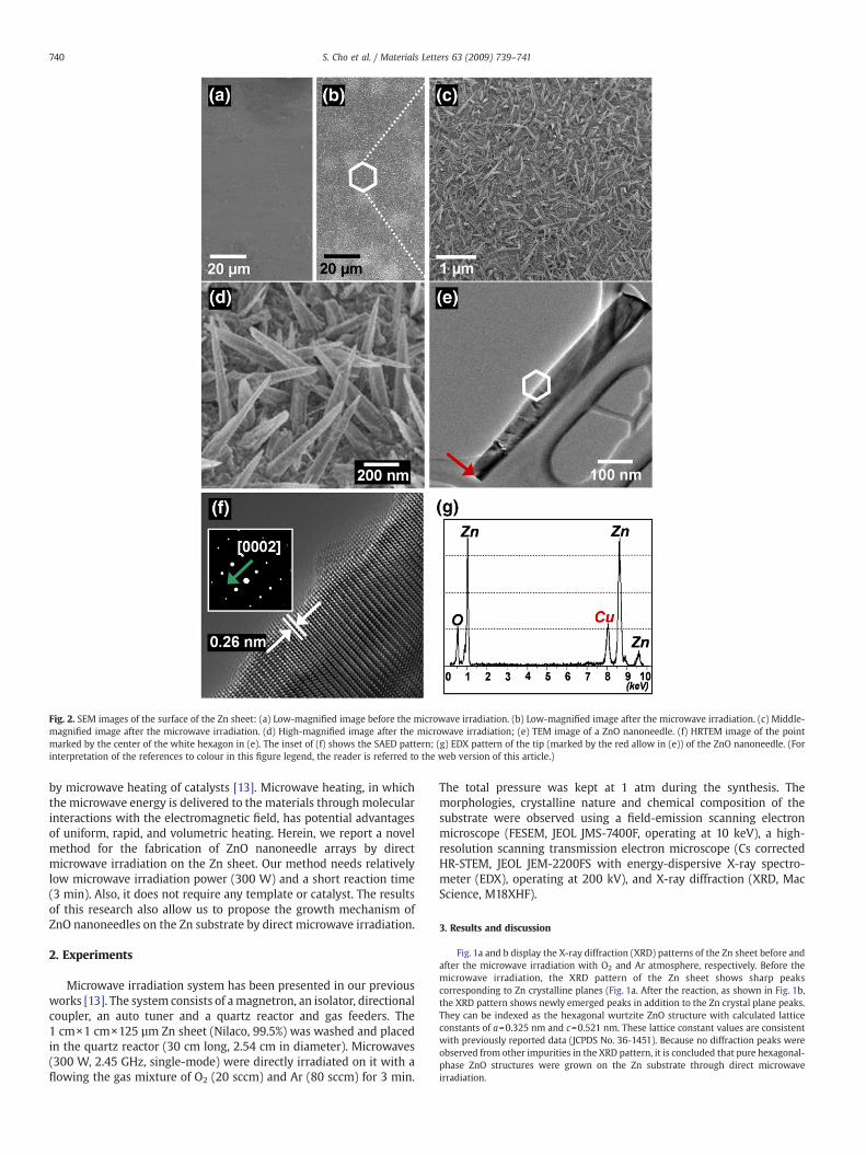
Fig. 2. SEM images of the surface of the Zn sheet: (a) Low-magnified image before the microwave irradiation. (b) Low-magnified image after the microwave irradiation. (c) Middle-magnified image after the microwave irradiation. (d) High-magnified image after the microwave irradiation; (e) TEM image of a ZnO nanoneedle. (f) HRTEM image of the pointmarked by the center of the white hexagon in (e). The inset of (f) shows the SAED pattern; (g) EDX pattern of the tip (marked by the red allow in (e)) of the ZnO nanoneedle. (Forinterpretation of the references to colour in this figure legend, the reader is referred to the web version of this article.)
740 S. Cho et al. / Materials Letters 63 (2009) 739–741
by microwave heating of catalysts [13]. Microwave heating, in whichthe microwave energy is delivered to the materials through molecularinteractions with the electromagnetic field, has potential advantagesof uniform, rapid, and volumetric heating. Herein, we report a novelmethod for the fabrication of ZnO nanoneedle arrays by directmicrowave irradiation on the Zn sheet. Our method needs relativelylow microwave irradiation power (300 W) and a short reaction time(3 min). Also, it does not require any template or catalyst. The resultsof this research also allow us to propose the growth mechanism ofZnO nanoneedles on the Zn substrate by direct microwave irradiation.
2. Experiments
Microwave irradiation system has been presented in our previousworks [13]. The system consists of amagnetron, an isolator, directionalcoupler, an auto tuner and a quartz reactor and gas feeders. The1 cm×1 cm×125 µm Zn sheet (Nilaco, 99.5%) was washed and placedin the quartz reactor (30 cm long, 2.54 cm in diameter). Microwaves(300 W, 2.45 GHz, single-mode) were directly irradiated on it with aflowing the gas mixture of O2 (20 sccm) and Ar (80 sccm) for 3 min.
The total pressure was kept at 1 atm during the synthesis. Themorphologies, crystalline nature and chemical composition of thesubstrate were observed using a field-emission scanning electronmicroscope (FESEM, JEOL JMS-7400F, operating at 10 keV), a high-resolution scanning transmission electron microscope (Cs correctedHR-STEM, JEOL JEM-2200FS with energy-dispersive X-ray spectro-meter (EDX), operating at 200 kV), and X-ray diffraction (XRD, MacScience, M18XHF).
3. Results and discussion
Fig. 1a and b display the X-ray diffraction (XRD) patterns of the Zn sheet before andafter the microwave irradiation with O2 and Ar atmosphere, respectively. Before themicrowave irradiation, the XRD pattern of the Zn sheet shows sharp peakscorresponding to Zn crystalline planes (Fig. 1a. After the reaction, as shown in Fig. 1b,the XRD pattern shows newly emerged peaks in addition to the Zn crystal plane peaks.They can be indexed as the hexagonal wurtzite ZnO structure with calculated latticeconstants of a=0.325 nm and c=0.521 nm. These lattice constant values are consistentwith previously reported data (JCPDS No. 36-1451). Because no diffraction peaks wereobserved from other impurities in the XRD pattern, it is concluded that pure hexagonal-phase ZnO structures were grown on the Zn substrate through direct microwaveirradiation.
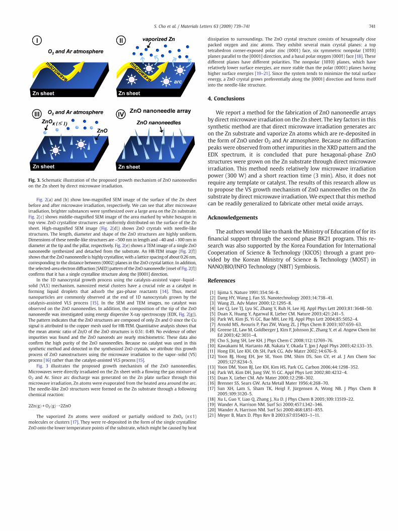
Fig. 3. Schematic illustration of the proposed growth mechanism of ZnO nanoneedleson the Zn sheet by direct microwave irradiation.
741S. Cho et al. / Materials Letters 63 (2009) 739–741
Fig. 2(a) and (b) show low-magnified SEM image of the surface of the Zn sheetbefore and after microwave irradiation, respectively. We can see that after microwaveirradiation, brighter substances were synthesized over a large area on the Zn substrate.Fig. 2(c) shows middle-magnified SEM image of the area marked by white hexagon intop view. ZnO crystalline structures are uniformly distributed on the surface of the Znsheet. High-magnified SEM image (Fig. 2(d)) shows ZnO crystals with needle-likestructures. The length, diameter and shape of the ZnO structures are highly uniform.Dimensions of these needle-like structures are ~500 nm in length and ~40 and ~100 nm indiameter at the tip and the pillar, respectively. Fig. 2(e) shows a TEM image of a single ZnOnanoneedle synthesized and detached from the substrate. An HR-TEM image (Fig. 2(f))shows that the ZnO nanoneedle is highly crystalline,with a lattice spacingof about 0.26 nm,corresponding to the distance between (0002) planes in the ZnO crystal lattice. In addition,the selected-area electron diffraction (SAED) pattern of the ZnOnanoneedle (inset of Fig. 2(f))confirms that it has a single crystalline structure along the [0001] direction.
In the 1D nanocrystal growth process using the catalysis-assisted vapor–liquid–solid (VLS) mechanism, nanosized metal clusters have a crucial role as a catalyst informing liquid droplets that adsorb the gas-phase reactants [14]. Thus, metalnanoparticles are commonly observed at the end of 1D nanocrystals grown by thecatalysis-assisted VLS process [15]. In the SEM and TEM images, no catalyst wasobserved on the ZnO nanoneedles. In addition, the composition of the tip of the ZnOnanoneedle was investigated using energy dispersive X-ray spectroscopy (EDX, Fig. 2(g)).The pattern indicates that the ZnO structures are composed of only Zn and O since the Cusignal is attributed to the copper mesh used for HR-TEM. Quantitative analysis shows thatthe mean atomic ratio of Zn/O of the ZnO structures is 0.51: 0.49. No evidence of otherimpurities was found and the ZnO nanorods are nearly stoichiometric. These data alsoconfirm the high purity of the ZnO nanoneedles. Because no catalyst was used in thissynthetic method and detected in the synthesized ZnO crystals, we attribute this growthprocess of ZnO nanostructures using the microwave irradiation to the vapor–solid (VS)process [16] rather than the catalyst-assisted VLS process [15].
Fig. 3 illustrates the proposed growth mechanism of the ZnO nanoneedles.Microwaves were directly irradiated on the Zn sheet with a flowing the gas mixture ofO2 and Ar. Since arc discharge was generated on the Zn plate surface through thismicrowave irradiation, Zn atoms were evaporated from the heated area around the arc.The needle-like ZnO structures were formed on the Zn substrate through a followingchemical reaction:
2Zn gð Þ + O2 gð ÞY2ZnO
The vaporized Zn atoms were oxidized or partially oxidized to ZnOx (x≤1)molecules or clusters [17]. They were re-deposited in the form of the single crystallineZnO onto the lower temperature points of the substrate, which might be caused by heat
dissipation to surroundings. The ZnO crystal structure consists of hexagonally closepacked oxygen and zinc atoms. They exhibit several main crystal planes: a toptetrahedron corner-exposed polar zinc (0001) face, six symmetric nonpolar {101 ̄0}planes parallel to the [0001] direction, and a basal polar oxygen (0001̄) face [18]. Thesedifferent planes have different polarities. The nonpolar {101̄0} planes, which haverelatively lower surface energies, are more stable than the polar (0001) planes havinghigher surface energies [19–21]. Since the system tends to minimize the total surfaceenergy, a ZnO crystal grows preferentially along the [0001] direction and forms itselfinto the needle-like structure.
4. Conclusions
We report a method for the fabrication of ZnO nanoneedle arraysby direct microwave irradiation on the Zn sheet. The key factors in thissynthetic method are that direct microwave irradiation generates arcon the Zn substrate and vaporize Zn atoms which are re-deposited inthe form of ZnO under O2 and Ar atmosphere. Because no diffractionpeaks were observed from other impurities in the XRD pattern and theEDX spectrum, it is concluded that pure hexagonal-phase ZnOstructures were grown on the Zn substrate through direct microwaveirradiation. This method needs relatively low microwave irradiationpower (300 W) and a short reaction time (3 min). Also, it does notrequire any template or catalyst. The results of this research allow usto propose the VS growth mechanism of ZnO nanoneedles on the Znsubstrate by direct microwave irradiation. We expect that this methodcan be readily generalized to fabricate other metal oxide arrays.
Acknowledgements
The authors would like to thank the Ministry of Education of for itsfinancial support through the second phase BK21 program. This re-search was also supported by the Korea Foundation for InternationalCooperation of Science & Technology (KICOS) through a grant pro-vided by the Korean Ministry of Science & Technology (MOST) inNANO/BIO/INFO Technology (NBIT) Symbiosis.
References
[1] Iijima S. Nature 1991;354:56–8.[2] Dang HY, Wang J, Fan SS. Nanotechnology 2003;14:738–41.[3] Wang ZL. Adv Mater 2000;12:1295–8.[4] Lee CJ, Lee TJ, Lyu SC, Zhang Y, Ruh H, Lee HJ. Appl Phys Lett 2003;81:3648–50.[5] Duan X, Huang Y, Agarwal R, Lieber CM. Nature 2003;421:241–5.[6] Park WI, Kim JS, Yi GC, Bae MH, Lee HJ. Appl Phys Lett 2004;85:5052–4.[7] Arnold MS, Avouris P, Pan ZW, Wang ZL. J Phys Chem B 2003;107:659–63.[8] Greene LE, Law M, Goldberger J, Kim F, Johnson JC, Zhang Y, et al. Angew Chem Int
Ed 2003;42:3031–4.[9] Cho S, Jung SH, Lee KH. J Phys Chem C 2008;112:12769–76.[10] Kawakami M, Hartanto AB, Nakata Y, Okada T. Jpn J Appl Phys 2003;42:L33–35.[11] Hong EH, Lee KH, Oh SH, Park CG. Adv Mater 2002;14:676–9.[12] Yoon BJ, Hong EH, Jee SE, Yoon DM, Shim DS, Son GY, et al. J Am Chem Soc
2005;127:8234–5.[13] Yoon DM, Yoon BJ, Lee KH, Kim HS, Park CG. Carbon 2006;44:1298–352.[14] Park WI, Kim DH, Jung SW, Yi GC. Appl Phys Lett 2002;80:4232–4.[15] Duan X, Lieber CM. Adv Mater 2000;12:298–302.[16] Brenner SS, Sears GW. Acta Metall Mater 1956;4:268–70.[17] Sun XH, Lam S, Sham TK, Heigl F, Jürgensen A, Wong NB. J Phys Chem B
2005;109:3120–5.[18] Xu L, Guo Y, Liao Q, Zhang J, Xu D. J Phys Chem B 2005;109:13519–22.[19] Wander A, Harrison NM. Surf Sci 2000;457:L342–346.[20] Wander A, Harrison NM. Surf Sci 2000;468:L851–855.[21] Meyer B, Marx D. Phys Rev B 2003;67:035403–1–11.