faq's - nanotechnology and engineered · pdf filefrequently asked questions...
TRANSCRIPT

Frequently asked
questions
Nanotechnology and Engineered Nanomaterials
A Primerauthors:
Andrew W. Salamon, Patrick Courtney and Ian Shuttler
Introduction
In recent years there has been ever increasing activity and excitement within the scientific and engineering communities, driven heavily by government investment, about engineered nanotechnology applications. The U.S. National Science Foundation has estimated that the global nanotechnology market could be worth U.S.$1 trillion by 2015.1 In parallel, much has been written and presented about the excitement and possible dangers of these materials. The tone of these media articles range from how these wonder materials are going to revolutionize all aspects of our lives to how they might kill us! The purpose of this primer is to provide some basic information about engineered nanomaterials so that you will be better informed, understand the new ‘jargon’ and appreciate some of the potential new applications of these materials. In addition, understanding the wide range and types of measurements needed to characterize these nanomaterials along with what solutions PerkinElmer has to support customers working in this field are outlined.

2
Table of Contents
What is nanotechnology? 3
What is the market and potential of nanotechnology? 4
What are engineered nanomaterials? 4
Fullerenes, graphene and carbon nanotubes 5
Quantum dots 5
Nanoparticles 6
Nanofibers and Nanowires 6
Where are nanomaterials being used today and in the future? 7
How are nanomaterials characterized? 7
What analytical techniques are used to characterize nanomaterials? 12
What are the environmental implications of nanotechnology? 13
What solutions are provided by PerkinElmer for nanomaterials characterization? 15
Where can I find more information? 16
References 16
Useful books and websites for more information 19
3
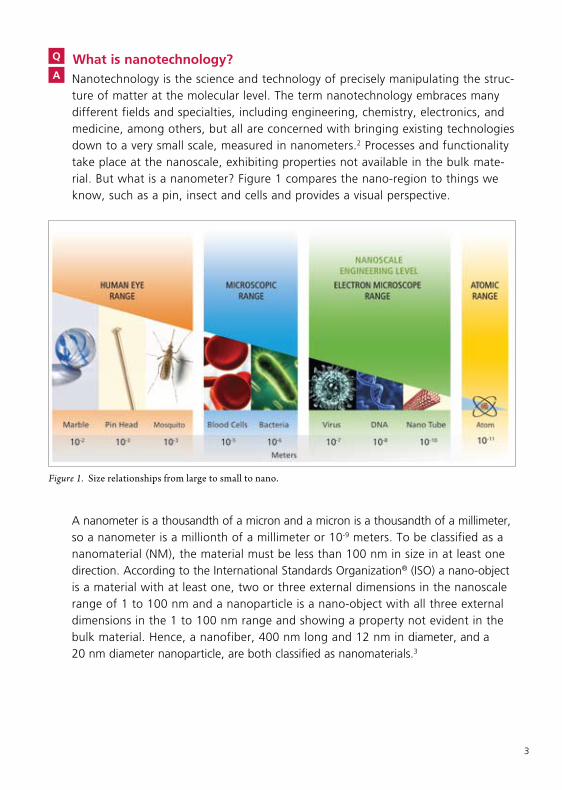
Q What is nanotechnology?A Nanotechnology is the science and technology of precisely manipulating the struc-
ture of matter at the molecular level. The term nanotechnology embraces many different fields and specialties, including engineering, chemistry, electronics, and medicine, among others, but all are concerned with bringing existing technologies down to a very small scale, measured in nanometers.2 Processes and functionality take place at the nanoscale, exhibiting properties not available in the bulk mate-rial. But what is a nanometer? Figure 1 compares the nano-region to things we know, such as a pin, insect and cells and provides a visual perspective.
Figure 1. Size relationships from large to small to nano.
A nanometer is a thousandth of a micron and a micron is a thousandth of a millimeter, so a nanometer is a millionth of a millimeter or 10-9 meters. To be classified as a nanomaterial (NM), the material must be less than 100 nm in size in at least one direction. According to the International Standards Organization® (ISO) a nano-object is a material with at least one, two or three external dimensions in the nanoscale range of 1 to 100 nm and a nanoparticle is a nano-object with all three external dimensions in the 1 to 100 nm range and showing a property not evident in the bulk material. Hence, a nanofiber, 400 nm long and 12 nm in diameter, and a 20 nm diameter nanoparticle, are both classified as nanomaterials.3
4
Even though ISO does not distinguish between engineered nanoparticles and naturally occurring nanoparticles, you should be aware that there are naturally occurring nanoparticles in the aquatic environment such as biodegraded organic matter and colloidal inorganic species and in soils; clays, organic matter and various metal oxides.4 Many important functions of living organisms take place at the nano-scale. The human body uses natural nanoscale materials such as proteins and other molecules, to control the body’s many systems and processes. A typical protein such as hemoglobin, which carries oxygen through the bloodstream, is 5 nm in diameter.5 However, this primer concentrates on Engineered Nanomaterials (ENMs).
Q What is the market and potential of nanotechnology?A
Last year the Russian government announced that it was investing $11 billion in an ambitious plan to develop and commercialize nanotechnologies.7 It is not only gov-ernments that are investing heavily in this area, venture capital firms invested $702M in nanotechnology start-ups in 2007 across 61 investments. The Japanese Mitsubishi Institute projected nanotechnology to be worth U.S.$150 billion on the global market by 2010 and Lux Research® estimated a U.S.$2.6 trillion global market by 2014.1 The U.S. NNI continues to be well funded with a 2010 budget of $1.6B, with total spending since 2001 of nearly $14B. However, to put some of these numbers into perspective, allocation of NNI funds for environmental, health and safety research since 2005 totals $480M.8 In spite of this it is clear that significant investments are being made in all aspects of nanotechnology and that there is considerable potential.
Q What are engineered nanomaterials?A There are many new material terminologies associated with this field. This section
gives a short overview of some of the different types of nanomaterials.
According to the U.S. National Nanotechnology Initiative (NNI), Federal Government funding in the United States, for nanotechnology, has increased from approximately $464 million in 2001 to nearly $1.9 billion for the 2010 fiscal year. Private industry is investing at least as much as the government, according to estimates. The United States is not the only country to recognize the tremendous economic potential of nanotech-nology. While it is difficult to measure accurately, estimates from 2005 showed the European Union (EU) and Japan are investing approximately $1.5 billion and $1.8 billion, respectively, in nanotechnology. Behind them were Korea, China and Taiwan with $300 million, $250 million and $110 million respectively, invested in nanotechnology research and development.6

5
Fullerenes, graphene and carbon nanotubes
A Fullerene is any molecule in the form of a hollow sphere, ellipsoid or tubular structure composed entirely of carbon. They are commonly referred to as “Buckyballs” – named after Buckminster Fuller who designed geodesic physical structures and buildings based on this geometry. A Buckyball is a carbon based hollow geometric sphere, first found in soot developed from a laboratory experiment.
It resembles a hollow spherical geodesic dome and is comprised of 60 carbon atoms (C60). Discovered in 1985, it is the roundest and most symmetrical large molecule known to man.9 Fullerenes or Buckyballs are used in nanotechnology. Graphene is a one atom thick planar sheet of carbon atoms densely packed in a honeycomb crystal lattice. Graphene is the basic structural building block of carbon nanotubes and fullerenes. Carbon nanotubes (CNT) also known as ‘buckytubes’ have a cylindrical nanostructure in the form of a tube and an engineered CNT typically has a nanoscale thick wall, geometrically shaped similar to a Buckyball, with a nanoscale diameter, and a length that may exceed 100 nm.
Carbon nanotubes are manufactured as single wall carbon nanotubes (SWCNT) or multiwall car-bon nanotubes (MWCNT). An example is shown in Figure 3. They are synthesized in a variety of ways, including arc discharge, laser ablation and chemical vapor deposition. With respect to tensile strength, carbon nanotubes are the strongest and stiffest materials yet discovered, more than 5 times stronger than Kevlar®. Since CNTs have a very low density, their specific strength is 300 times greater
than stainless steel, though under compression CNTs appear to be a lot weaker.
Quantum dots
Quantum dots, also known as nanocrystals, are another form of nanomaterial and are a specific type of semiconductor. They are 2-10 nanometers (10-50 atoms) in diameter, and because of their electrical characteristics, they are [electrically] tun-able.10 The electrical conductivity of semiconductors can change due to external stimulus such as voltage or exposure to light, etc. As quantum dots have such a
Figure 3. Multiwalled carbon nanotube.
Figure 2. C60 buckyball.

6
small size they show different properties to bulk material. Hence the ‘tunability’, for example, sensitivity to different wavelengths of light, can be adjusted by the number of atoms or size of the quantum dot. Quantum dots are typically made from CdSe, ZnS or CdTe compounds, though from a EU Restriction of Hazardous Substances (RoHS) perspective, cadmium-free quantum dots are required.11 For an excellent explanation of quantum dots and their operation in a cadmium selenide semiconductor see the website associated with reference.10
Nanoparticles
Nanoparticles (NP) are synthesized or machined. They range in size from 2 nm to 100 nm. Nanoparticle materials vary depending on their application. Because Nanoparticles are invisible to the naked eye, they are usually supplied suspended in a liquid. This is done for safety and handling reasons. Figure 4 shows gold nanoparticles suspended in liquid. The color is due to the refraction of light the surface area of the particular nanoparticle reflects. Different sized nanoparticles exhibit different colors based on its surface area.12
Figure 4. Suspension of gold nanoparticles.
Figure 5. SEM image of aligned nanofibers. Photo courtesy of Univ. of Wisconsin – Madison, Department of Chemistry.
Nanofibers and Nanowires
Nanofibers are slightly larger in diameter than the typical nanomaterial definition, though still invisible to the naked-eye. Their size ranges between 50 nm - 300 nm in diameter and are generally produced by electro spinning in the case of inor-ganic nanofibers or catalytic synthesis for carbon nanotubes. Figure 5 shows an SEM image of aligned nanofibers. Nanofibers can be electrostatically aligned and biochemically aligned.13,14 Further information about nanofibers fabrication can be found in reference.15 Similar to nanofibers are nanowires, though nanowires are considerably smaller in diameter, of the order of 4 nm and conduct electricity.
In Table 1, the different size characteristics of the various nanomaterials are summarized.

7
Table 1. Nanomaterial types and dimension characteristics.
Type of Nanomaterial Number of dimensions and size
Nanoparticle Three dimensions in the 1 to 100 nanometers (nm) range
Nanotubes/nanowires Two dimensions in the 1 to 100 nm range
Nanofibers Length ranges between 50 nm and 300 nm with diameter <50 nm
Nanofilms One dimension in the 1 to 100 nm range
Nanoplates Two dimensions in the 1 to 100 nm range
Q Where are nanomaterials being used today and in the future? A Some of the current applications of many of these nano-related materials and
technology are outlined in Table 2 (Page 8). While this table is not intended to be exhaustive, it does show how wide ranging the applications are. It is clear that the nanomaterial science revolution has the potential and magnitude to be an enormous leap forward in technology. However, it should be noted that there are increasing concerns about the impact of these materials in the environment and their possible impact on human health.
Currently the Woodrow Wilson Center for Scholars through their Project on Emerging Nanotechnologies (PEN) lists in their database, 1015 commercially available nanotechnology containing consumer products in over 20 countries16 up to 2009. This website and searchable database is recommended for those wishing to learn more.
A more comprehensive listing of current and possible future applications of nanomaterials is available on www.PerkinElmer.com/nano
Q How are nanomaterials characterized?A It is important to understand that the excitement regarding the synthesis and
application of nanomaterials is based on the fact that, because of their very small size, the characteristics and behavior are quite different to bulk materials with the same composition. Consequently, the range of parameters that has to be assessed to characterize these materials is large. Fundamentally there are seven key characteristics that contribute to the uniqueness of nanomaterials and these are summarized in Table 3.
In addition to the key seven characteristics, there are two additional qualities that are unique to nanomaterials and important in characterizing them. These are agglomeration, which is the tendency of the particles to clump together and form larger combined particles, and the particle size distribution.

8
Table 2. Selection of nanomaterials and usage or application area.
Market Industry Type of Use/Application Area Segment Nanomaterial
Environmental Water Nano zero valent Being tested for the remediation of ground and surface waters iron (nZVI) exposed to chlorinated hydrocarbons17
Gold nanoparticles Various gold nanomaterials are used to enhance imaging properties of a variety of MRI and CT-based contrast agents18
UV absorbing Improved and sustainable water based surface coatings to nanomaterials protect and preserve wood, concrete and metal surfaces used in construction19
Safety and Food Clay Nanomaterials are being used in food packaging. The Security penetration of light, moisture, or gases can alter the sensory characteristics of food products, as well as increase spoilage. Nanomaterials enhance packaging barrier properties20
Energy Pd and V doped Enhance hydrogen fuel cells by increasing storage capacities carbon nanotubes and showing faster hydrogen absorption kinetics21
Medical Various materials Nanomaterials coated with pharmaceutical compounds are being considered as novel inhalation delivery systems for medications difficult to administer by other means22
Textiles/ Silver nanoparticles Integrated with sports clothing to prevent microbial growth, Apparel and odor23,24
Cosmetics/ Nano titanium Used in some cosmetics. The applications include: eye liners, Personal dioxide and nano moisturizers, lipsticks, make-up foundations, soaps, sunscreen, Care Products zinc oxide mascara, and nail polish16
Industrial Defense CNTs Body armor – multilayer-epoxy composites manufactured with CN sheets, the size of a piece of plywood 4’ x 8’ foot, provide a shield that can stop a 9 mm bullet and weighs no more than a pack of playing cards25
Aerospace Clay nanoparticles Incorporated with thermoplastics to create improved fire retardant aircraft interiors26
Automotive 10 nm Cerium oxide Forms part of the Envirox™ diesel fuel catalyst which improves nanoparticles combustion due to the increased surface area of the cerium oxide nanoparticles27
Recreation/ Unknown Holmenkol® AG supply a chemical nanotechnology coating Manu- system under the brand name ‘Nanowax®’ to replace conven- facturing tional ski and snowboard waxes28
Sports CNTs/Yarn High end golf club shafts are made with nano-composites to make equipment the shaft stronger and more flexible. Racing bicycle components29

9
Table 3. Nanomaterial characteristics, their impact and importance.
Nanomaterial Characteristic Impact and Importance
Size Key defining criteria for a nanomaterial3 (see Table 1).
Shape Carbon nanosheets with a flat geodesic (hexagonal) structure show improved performance in epoxy composites versus carbon fibers.30
Surface Charge Surface charge is as important as size or shape. Can impact adhesion to surfaces and agglomeration characteristics. Nanoparticles are often coated or ‘capped’ with agents such as polymers (PEG) or surfactants to manage the surface charge issues.
Surface Area This is a critical parameter as the surface area to weight ratio for nanomaterials is huge. For example, one gram of an 8 nm diameter nanoparticle has a surface area of 32 m2. Nanoparticles may have occlusions and cavities on the surface.
Surface Porosity Many nanomaterials are created with zeolite-type porous surfaces. These engineered surfaces are designed for maximum absorption of a specific coating or to accommodate other molecules with a specific size
Composition The chemical composition of nanomaterials is critical to ensure the correct stoichiometry has been achieved. The purity of nanomaterials, impact of different catalysts used in the synthesis and presence of possible contaminants needs to be assessed along with possible coatings that may have been applied.
Structure Knowledge of the structure at the nano level is important. Many nanomaterials are hetero- geneous and information concerning crystal structure and grain boundaries is required.
Figure 6. Key parameters to characterize nanomaterials.
10
Q What analytical techniques are used to characterize nanomaterials?A As shown in Figure 6 there are seven key characteristics along with agglomeration
and particle size distribution that need to be measured to fully describe a nano-material. Consequently, at the nanoscale, analytical measurement challenges are considerable and the ability to use, for example, one technique such as inductively coupled plasma-mass spectrometry (ICP-MS) to measure the elemental concentration of gold in a suspension of gold nanoparticles as the only metric to assess the material, does not provide all the information needed. To completely characterize the material it is necessary to know a multitude of chemical and physical parameters including; the size of the particles, their shape, surface characteristics, presence of any surface coating and presence of impurities. This small subset illustrates the magnitude of the measurement challenge facing the nanomaterials industry. Table 4 lists the key characteristics and many of the current analytical technologies that can be applied.
In addition to looking at a variety of analytical techniques and their application to nanomaterials it is also important to understand where measurements need to be made, what type of measurements are required and why. To understand this, an overview of the nanomaterial manufacturing process and value chain is necessary. This includes consideration of aspects such as source and quality of raw materials, control of the synthesis/manufacturing process, validation of the final product and subsequent use or incorporation into another product, e.g., a cosmetic preparation. Along this manufacturing chain are a variety of points at which material and hazardous waste may need to be disposed of and there is potential for environmental exposure. Figure 7 provides a high level view of this process in a very fast changing technology area and outlines which characteristics may need to be assessed at the various measurement points. To understand which analytical technologies may be required to provide this information, Figure 7 and Table 4 can be compared. This chain has been developed from recent market research and customer feedback.
Key nanomaterial characteristics require new measurement technologies. An analyti-cal technique that is becoming more prevalent in the nanomaterial field is that of Field Flow Fractionation (FFF) coupled with Light Scattering (LS) and possibly ICP-MS for elemental nanoparticle characterization. Field Flow Fractionation is a separation technique similar to chromatography whereby colloids, macromolecules and nanoparticles are separated by size and should allow a separation of natural and engineered nanomaterials. Further details can be found in a recent review article on the coupling of FFF with ICP-MS31 and the websites under references.32,33

11
Figure 7. High-level overview of the engineered nanomaterial manufacturing process and key characteristics.
Electron microscopy is also widely used to characterize nanoparticles. The surface area, porosity, particle shape, and agglomeration can be examined with Scanning Electron Microscopes (SEM), Atomic Force Microscopes (AFM), Tunneling Electron Microscopes (TEM), and Confocal Microscopes.
In the production and characterization of carbon nanotubes (CNTs) the use of Thermogravimetric Analysis (TGA) has found considerable application and can be used to show batch to batch reproducibility, detect changes in the process and validate purification protocols.34 During both the production and formulation process, many nanoparticles are coated or ‘capped’ with a variety of molecules. For assessing the coating, the hyphenated technique of TGA coupled with GC/MS is finding use.35 A critical application in this area is determining the amount of anti-cancer drug that is coated on nanoparticles. This is needed to characterize the dosage being consumed by the patient.
Q What are the environmental implications of nanotechnology?A Process waste has always been a manufacturing issue. It is slightly different today
when nanoparticles are considered. Nano-waste is different than bulk material waste. It’s been seen in laboratory experiments that nanomaterials can enter the human body by dermal exposure, inhalation, and ingestion.36 While there are no specific nanomaterials regulations, yet, there is increasing review and concern both within the industry and in the environmental field as to the fate and behavior of these materials in the environment. Many nanomaterial manufacturers are following bulk material

Table 4. Nanomaterial characteristics and applicable analytical technologies.
Nanomaterial Characteristics Concentration Particle Size Particle Size Surface Surface Shape Agglomeration Structure Composition Analytical Technique Distribution Charge Area
Inductively Coupled Plasma – Mass Spectrometry ICP-MS
Field-flow Fractionation + ICP-MS FFF-ICP-MS
Liquid Chromatography – Mass Spectrometry LC-MS
Optical Spectroscopy – UV/Vis UV/Vis
Fluorescence Spectroscopy FL
Turbidity
Scanning Electron Microscopy SEM
Transmission Electron Microscopy (+EDX) TEM
Atomic Force Microscopy AFM
Confocal Microscopy
Field Flow Fractionation FFF
Dynamic Light Scattering DLS
Static Light Scattering SLS
Molecular Gas Adsorption (BET) BET
Dialysis
Electrophoresis and Capillary Electrophoresis
Ultrafiltration
Centrifugation
Filtration
Nanoparticle Tracking Analysis NTA
Size Exclusion Chromatography SEC
Selected Area Electron Diffraction SAED
Zeta Potential by DLS
X-ray Diffraction XRD
Thermogravimetric Analysis TGA
Quartz Microbalances
Differential Scanning Calorimetry DSC
Dynamic Mechanical Analysis DMA
Fourier Transform Infrared Spectroscopy FT-IR
FT-IR Imaging
Raman Spectroscopy
TGA coupled with Gas Chromatography – Mass Spectrometry TGA-GC/MS
Laser Induced Plasma Spectroscopy LIPS
Hydrodynamic Chromatography HDC
Laser Induced Breakdown Detection LIBD
X-ray Photoelectron Spectroscopy XPS
Electron Energy Loss Spectroscopy EELS (+EDX)
Commonly used in the characterization of nanomaterials
Microscopy techniques

13
Table 4. Nanomaterial characteristics and applicable analytical technologies.
Nanomaterial Characteristics Concentration Particle Size Particle Size Surface Surface Shape Agglomeration Structure Composition Analytical Technique Distribution Charge Area
Inductively Coupled Plasma – Mass Spectrometry ICP-MS
Field-flow Fractionation + ICP-MS FFF-ICP-MS
Liquid Chromatography – Mass Spectrometry LC-MS
Optical Spectroscopy – UV/Vis UV/Vis
Fluorescence Spectroscopy FL
Turbidity
Scanning Electron Microscopy SEM
Transmission Electron Microscopy (+EDX) TEM
Atomic Force Microscopy AFM
Confocal Microscopy
Field Flow Fractionation FFF
Dynamic Light Scattering DLS
Static Light Scattering SLS
Molecular Gas Adsorption (BET) BET
Dialysis
Electrophoresis and Capillary Electrophoresis
Ultrafiltration
Centrifugation
Filtration
Nanoparticle Tracking Analysis NTA
Size Exclusion Chromatography SEC
Selected Area Electron Diffraction SAED
Zeta Potential by DLS
X-ray Diffraction XRD
Thermogravimetric Analysis TGA
Quartz Microbalances
Differential Scanning Calorimetry DSC
Dynamic Mechanical Analysis DMA
Fourier Transform Infrared Spectroscopy FT-IR
FT-IR Imaging
Raman Spectroscopy
TGA coupled with Gas Chromatography – Mass Spectrometry TGA-GC/MS
Laser Induced Plasma Spectroscopy LIPS
Hydrodynamic Chromatography HDC
Laser Induced Breakdown Detection LIBD
X-ray Photoelectron Spectroscopy XPS
Electron Energy Loss Spectroscopy EELS (+EDX)
Not widely applicable
Available from PerkinElmer

13
regulations and working with the EPA to establish nanomaterial guidelines for health and safety for the workers and for the end users. The EPA has declared that nano- carbon is a new material and use and requires that it be substantiated as safe.37 So airborne nanoparticles, nanoparticles in water, and skin exposure to nanomaterials are being addressed by all parties concerned, but there is much research to be done and a key aspect of this work is the need for methods and analytical techniques that can separate, identify and quantitate ENPs in amongst naturally occurring nanoparticles. As consumers, we should to be aware of nanoparticles in the products we use and the food we eat, but currently there are no labeling regulations. There is legislation being implemented in Europe that requires cosmetic manufacturers to list any nanoparticles used in their products.38,39 This is the first European industry to have required labeling. To date labeling is not required for any other industries anywhere in the world.
Within the United States, the EPA and other government agencies are proactive in regards to nanotechnology. The Federal Government has established the National Nanomaterial Initiative (NNI) where government agencies and private industry meet to discuss and understand nanomaterial implications of the environment and human health. PerkinElmer participates in NNI meetings and is working with the EPA and other agencies to better understand nanomaterials. Figure 8 depicts the life cycle of nanomaterials in the environment and identifies what government agencies are addressing these segments of the life cycle. The source and emission in Figure 8 corresponds to the manufacturing waste in figure 7. The waste interaction with the environment could occur from material taken to a dump, incinerated or washed down the drain. Environmental Health and Safety (EHS) applies to nanomaterial workers as human exposure could occur during the manufacturing process.
Figure 8. Nanomaterial life cycle in the environment.Source: DOE Molecular Foundry – Lawrence Berkeley National Laboratory.

14
Q What solutions are provided by PerkinElmer for nanomaterials characterization?A Although nanomaterials are small and cannot be seen with the naked eye, it seems likely
that their impact on the world will be huge. PerkinElmer is involved in the nanomaterial revolution by participating and working with government agencies, research universities, nanomaterial manufacturers, and end-user industries. While PerkinElmer does not supply all the possible measurement technologies required as listed in Table 4, in certain important areas we have a rich solution offering to enable customers to make critical measure- ments. As customers discover what measurement parameters and performance criteria are important, we believe that our offerings will deliver more value and come to be recognized as important solutions to challenging problems.
PerkinElmer has the following solutions available for customers who require nanomaterial characterization:
Table 5. PerkinElmer analytical solutions.
Analytical Technology Application
UV/Vis The LAMBDA™ 850/950 are being used to assess nanomaterial surface coating on glass for the solar energy industry. The LAMBDA 1050 equipped with a 150 mm integrating sphere has been used to measure the band gap (an important semiconductor characteristic) of TiO2 nanomaterials.40
Fluorescence The LS-55 is being used to measure the fluorescence shift in quantum dots. In addition, quantum dots are being considered as reference materials to calibrate fluorescence spectrometers.41
FT-IR Photocatylitic degradation of dyes and other photosensitive materials. Use of FT-IR imaging to examine gold nanostructures embedded in 50 nm thin polymethylmethacrylate film to develop novel materials.40
Raman Surface characterization of films and other substrate materials that are coated with nanomaterials.
TGA Pyris™ 1 TGA finds application in characterizing CNTs during the manufacturing process and for incoming inspection.
DSC DSC 8500 is being used to characterize amorphous pharmaceuticals that employ nanomaterials such as determining the glass transition temperature (Tg) to assess the nano-crystalline structure.40 StepScan™ and HyperDSC® have been used to study the rigid amorphous fraction in polymethylmethacrylate silicon oxide nano-composites.42
DSC-Raman Morphology characterization of SWCNTs in composites.
DMA To assess the strength of different composite mixtures of CNT/epoxy.
TGA-GC/MS Being used by an EPA lab to measure the degree of coating on ENPs under different conditions.
AA Mainly used to measure bulk concentrations in fabricated materials such as Ag nanoparticle impregnated fabrics [Ag in textile/Germany].
ICP Assessment of gold and copper concentration in digests of elemental nanomaterial suspensions.43
ICP-MS Rapidly becoming the elemental measurement technique of choice for ENPs, especially Au, Ag, Pt, Ce, W, Ti, etc. in the environment and increasingly being coupled with Field Flow Fractionation. In a recent review article on this hyphenated technique, of the 28 papers referenced, 18 used PerkinElmer® ICP-MS systems.31 Researchers are now looking to perform single particle analysis with ICP-MS as this gives additional size and distribution information.44

15
PerkinElmer is an active member of the ISO group establishing nanomaterial testing protocols and participates in NNI meetings and a variety of international nanomaterial scientific meetings.
Q Where can I find more information?A To learn more about PerkinElmer analytical solutions for nanomaterial applications,
please visit http://www.perkinelmer.com/nano. This will continue to develop in the future to provide access to key scientific publications, background information, application notes and links to useful websites.
This ‘Primer’ is intended to provide you with useful background information; it cannot answer every question, but it should stimulate material characterization discussions that hopefully will lead to an analytical solution.
Have questions, need more information? Please contact Andrew Salamon, Patrick Courtney or your local PerkinElmer sales representative. We are happy to answer your nano-related questions.
References
1. Burnett, K., and Tyshenko, M.G., (2010), A comparison of human capital levels and the future prospect of the nanotechnology industry in early sector investors and recent emerging markets, Intl. J. of Nanotechnology, 7, 2/3, 187-208. http:// www.inderscience.com/browse/index.php?journalID=54&year=2010&vol=7&issue=2/3
2. American Heritage Dictionary, March 2010. http://dictionary.reference.com/ browse/Nanotechnology
3. International Standards Organization, 2008, ISO/TS 27687:2008 and 2010, ISO/ CD TS 80004-1:2010
4. Klaine, S.J., Alvareez, J.J., Batley, G.E., et al., (2008), Critical Review, Nanomaterials in the environment: behaviour, fate, bioavailability and effects, Environ. Toxicol. Chem, 27, 1825-1851
5. National Nanomaterial Initiative, March 2010: http://www.nano.gov/Nanotechnology_ BigThingsfromaTinyWorldspread.pdf
6. National Nanomaterial Initiative, March 2010: http://www.nano.gov/html/facts/faqs.html
7. Nature, (2009), 461, 1036-1037, doi: 10.1038/4611036a
8. National Nanomaterials Initiative, 2010, Supplement to the President’s FY2011 budget http://www.nano.gov/NNI_2011_budget_supplement.pdf

16
9. Gion, A., (2010) Bucky Balls, March 2010: http://www.3rd1000.com/bucky/bucky.htm
10. Evident Technologies, (March 2010): http://www.evidenttech.com/quantum-dots- explained/how-quantum-dots-work.html
11. Nanoco Group PLC website, (2010), http://www.nanocotechnologies.com/content/ AboutUs/AboutQuantumDots.aspx
12. Nanocomposix Corp., (March 2010): http://www.nanocomposix.com/product-gold/ nanoxact-gold.html
13. Li, D., Wang, Y., Xia, Y., (2004), Electrospinning Nanofibers as Uniaxially Aligned Arrays and Layer-by-Layer Stacked Films, Adv. Matls., 16, 4, 361-366, DOI 10.1002/adma.200306226, http://www3.interscience.wiley.com/journal/107630203/ abstract
14. Patel, S., Li, S., (2007), Bioactive Aligned Nanofibers for Nerve Regeneration, Nanotech Conference, Santa Clara, CA, USA. http://www.nsti.org/BioNano2007/ showabstract.html?absno=1301
15. Hegde, R.R., Dahiya, A., Kamath, M.G., (2005), Nanofiber nonwovens, http://web. utk.edu/~mse/Textiles/Nanofiber Nonwovens.htm
16. Woodrow Wilson Center for Scholars, Project on Emerging Technologies (2010), http://www.wilsoncenter.org/index.cfm?topic_id=166192&fuseaction=topics.home
17. Nanoiron Future Technology, Rajhard, Czech Republic, http://www.nanoiron.cz/en/ home-page
18. Moriggi, L., Cannizzo, C., Dumes, E, et al., (2009), Gold Nanoparticles Functionalized with Gadolinium Chelates as High-Relaxivity MRI Contrast Agents, J. Am. Chem. Soc., 131 (31), pp 10828–10829, DOI: 10.1021/ja904094t,
19. Nanovations Pty, Ltd., New South Wales, Australia, (2010), http://www.nanovations.com.au/index.htm
20. Nanocor, USA, www.nanocor.com
21. A to Z of Nanotechnology website, (2010), http://www.azonano.com/details.asp? ArticleID=1339
22. Yang, W., Peters, J.I., Williams III, R.O., (2010), Inhaled nanoparticles – a current review., Int. J. of Pharmaceutics, 356, 1-2, 239-247, doi:10.1016/j.ijpharm.2008. 02.011
23. 3XDRY® Essex Fishing Shirt, (2010). http://www.simmsfishing.com/site/3xdry_essex_ shirt.html#
24. PuckSkin Hockey Apparel, BC, Canada, (2010), http://www.puckskin.com/home.htm

25. Nanocomp Technologies, Concord, NH; USA, (2010), http://www.nanocomptech. com/html/nanocomp-what-we-do.html
26. Federal Aviation Administration, Fire Safety Division, Washington DC, USA, (2010), http://www.fire.tc.faa.gov/research/targtare.stm
27. Energenics web page, suppliers of Envirox™ http://www.energenics.org/envirox.html
28. Holmenkol AG, Germany, (2010), http://www.nanowax.de/index.php?id=10&L=1
29. Easton Sports Inc., CA, USA, http://eastonbike.com/
30. Goa, F., University of Nottingham Trent, UK, January 26, 2010, Lecture Presentation
31. Dubascoux, S., Le Hecho, I., Hassellöv, M., et al, (2010), Field-flow fractionation and inductively coupled plasma mass spectrometer coupling: History, development and applications. J. Anal. Atom. Spectrom, DOI: 10.1039/b927500b, web prepublication 23-March-2010
32. Postnova Corp., Germany, (2010), http://www.postnova.com/
33. Wyatt Technology Corporation,USA, (2010), http://www.wyatt.com/
34. Mansfield,E., Kar, A, Hooker, S.A., (2010), Applications of TGA in quality control of SWCNTs, Anal. Bioanal. Chem., 396(3), 1071-1077.
35. Sahle-Demesie, E., EPA, USA, (March 2010), Personal communication with A. Salamon, PerkinElmer
36. National Nanotechnology Initiative - Human Health Workshop (2009), Washington DC., USA, November 17 – 18.
37. Environmental Protection Agency, Washington DC, USA, (2010), Control of nanoscale materials under the Toxic Substances Control Act, http://www.epa.gov/oppt/nano/
38. European Union Cosmetics directive, 76/768/EEC, 25 March 2009
39. Bowman, D.M., van Calster, G., Friedrichs, S., (2010), Nanomaterials and regulation of cosmetics, Nature Nanotechnology 5, 92 doi:10.1038/nnano.2010.12
40. Courtney, P., (2009), Functional measurements in nanomaterisals using optical and thermal techniques, PerkinElmer poster presented at the 3rd Nanomaterials Conference, Bonn, Germany, 16 – 18 June. http://www.nanotechia.org/events/ nanomaterials-2009
41. Upstone, S., Seer Green, UK, (2008), PerkinElmer Presentation, Colloquium on Optical Spectroscopy (COSP), Berlin, Germany
42. Schick, C., (2009), Study Rigid Amorphous Fraction in Polymer Nano-Composites by Step Scan and Hyper DSC, PerkinElmer Application Note #008648_01
43. Sarojam, P., (2010), Elemental characterization of gold and copper nanoparticles with ICP-OES, PerkinElmer Application Note (in preparation)
17
18
44. Heithmar, E.M., and Siska, E.M., (2010), Single particle-inductively coupled plasma mass spectrometry of metal-containing nanomaterial in surface waters around Las Vegas, Nevada, USA, Poster presentation at the 2010 Winter Conference on Plasma Spectrochemistry, Fort Myers, Florida, USA, January 4-9.
Useful books and websites for more information
Nanochemistry – A Chemical Approach to Nanomaterials, 2nd Edition, (2009), Ozin, G.A., Arsenault, A.C., Cademartiri, L.,RSC Publishing, Cambridge, UK, ISBN: 978-1-84755-895-4
Introduction to Nanoscience, (2010), Lindsay, S.M., Oxford University Press, Oxford, UK, ISBN: 978-019-954420-2
PerkinElmer Nano Applications Library, http://www.perkinelmer.com/nano
U.S. National Nanomaterials Initiative (NNI), http://www.nano.gov/
University of California Center for Environmental Implications of Nanomaterials, USA, http://cein.cnsi.ucla.edu/pages/
Duke University Center for the Environmental Implications of Nanotechnology, USA, http://www.ceint.duke.edu/
U.S. Department of Defense, Nano-Funding, http://nanosra.nrl.navy.mil/funding.php
Current Government Nanomaterial Solicitations, http://www.nano.gov/html/funding/currentsol.html
Nanotechnology Nanomaterial Suppliers, http://www.nanowerk.com/nanotechnology/nanomaterial/suppliers_plist.php?subcat1=np
Overview of ground water treatment and chemistry with nano zerovalent iron, http://cgr.ebs.ogi.edu/iron/
UK-based nanotechnology forum intended for anyone who wants to learn more about this technology, products etc., http://www.nanoandme.org/home/
Nanotechnology Now information forum, http://www.nanotech-now.com/nano_intro.htm
A to Z Nanotechnology, a free-to-access nanotechnology website, http://www.azonano.com/default.asp
Nanotechnologies Industry Association, Brussles, Belgium, (2010), http://www.nanotechia.org/content/aboutus/
The Nanotube Site. Very comprehensive listing of information and publications on carbon nanotubes. (2010). http://www.pa.msu.edu/cmp/csc/nanotube.html

For a complete listing of our global offices, visit www.perkinelmer.com/ContactUs
Copyright ©2010, PerkinElmer, Inc. All rights reserved. PerkinElmer® is a registered trademark of PerkinElmer, Inc. All other trademarks are the property of their respective owners. 009228_02
PerkinElmer, Inc. 940 Winter Street Waltham, MA 02451 USA P: (800) 762-4000 or (+1) 203-925-4602www.perkinelmer.com