federico alessio supervisors diego gamba, angelo rivetti richard jacobsson a complete system for...
TRANSCRIPT

Federico AlessioSupervisors
Diego Gamba, Angelo Rivetti
Richard Jacobsson
A complete system for controlling and monitoring
the timing of the LHCb experiment

Federico Alessio 21/12/2007 2
My work at CERN
Technical Student since February 2007
Involved in LHCb experiment at CERN, in the ONLINE group
Richard Jacobsson as CERN supervisor, project leader of the TFC System project (Timing and Fast Control System) http://lhcb-online.web.cern.ch/lhcb-online/TFC/default.html
Proposal of working on the coarse and fine time alignment of the experiment. The project involves the development of an electronics monitor board (Beam Phase and Intensity Monitor) for precise bunch-by-bunch measurements of the intensity and the phase of the LHC beams involving both analogue and digital electronics, and the development of GUI interfaces to monitor the information. Moreover, the control of a new system (RF2TTC System) provided by the LHC group has to be implemented to distribute the clock to the whole TFC system and then to the experiment. A User Interface will help the users to interact with the systems.
I have been also involved in the installing, commissioning and support of the whole TFC system and I took part to some sessions of the global LHCb commissioning.

Federico Alessio 21/12/2007 3
Intro: the LHC at CERN
Large Hadron Collider:
27 km of circumference and 36800 t of cold mass
proton-proton collider
14 TeV as centre-of-mass energy and 1011 protons per bunch
broad and suggestive physics studies (Higgs, SUSY, matter/antimatter, Big Bang)
most advanced technology ever considered
incredible cryogenic system with 96 t of liquid helium to cool the RF cavities down to 1.9 K 4 main experiments: ALICE, ATLAS, CMS, LHCb

Federico Alessio 21/12/2007 4
Intro: LHCb experiment
Measuring CP Violation in bbpp
located at Point 8 at CERN 103 metres underground fitting the pre-existing LEP cavern
single arm spectrometer, with angular coverage between 10 and 300 mrad in the bending plane of the magnetic field
displaced by 11.25m from the nominal interaction point along the LHC ring
comprises 10 different sub-systems which can be autonomously run and satisfies any need for the physics: mesons tracking or momentum/energy identification
Front-End Electronics (FEE) independent from each sub-detector
ready to run in summer 2008 at 14 TeV in the interaction point

Federico Alessio 21/12/2007 5
Intro: Read-Out System
clocked by the LHC at 40 MHz
lower the dataflow rate from 40 MHz to 2 KHz
lower the throughput of data transmitted from 40 TB/s to 4 GB/s
production of the L0 Trigger decision to make an hardware selection and packing of events (Multi-Event Packing Packages)
Everything managed by the TFC System which is the real heartbeat of the Read-Out system. It is responsible for controlling and distributing timing, trigger, synchronous and asynchronous commands to the LHCb Front-End Electronics. It is also responsible to distribute the clock to the electronics of the whole experiment through the RF2TTC board and to monitor bunch-by-bunch the LHC beam through the BPIM board.
push with pull dataflow protocol : data transferred to the next stage just when some new data is available while some information are sent back for data flow control

Federico Alessio 21/12/2007 6
Intro: TFC SystemTFC controls the readout part of the system accomplishing 4 main tasks:
control, monitoring and test runs: done by a pool of Readout Supervisors (ODINs)
partitioning: a TFC Switch allows to run sub-systems autonomously and makes independent tests (THOR)
feedback: done by the Throttle Switch to maintain the readout rate below the limits of the DAQ (Hugin and Munin)
coarse and fine time alignment: through the RF2TTC and the BPIM boards, it is possible to time align the whole LHCb experiment in a way that each sub-detector can produce a precise signal at the optimal point and that this signal is stable

Federico Alessio 21/12/2007 7
Motivations: LHCb Timing
Luminosity (L = 1032 cm-2 s-1 ) and Energy (E = 7 TeV) are crucial parameters in the LHC
Protons are accelerated in Radio Frequency cavities where a time-varying electrical field (sinusoidal) is applied at a frequency of 400.79 MHz.
In order to focus the beam longitudinally and result homogeneous, protons are injected in the LHC ring timed to cross the gap during the slope of the sinewave.
The RF system defines buckets ( 35640 in total ) in which the bunches of protons can sit, allowing for a structured beam. Two consecutive buckets are spaced by 2.5 ns and the resulting bunch length is between 1.17 ns and 1.06 ns.
The actual bunches of protons sit in position number 1, 11, 21, 31, etc… which means that two consecutive bunches with protons are spaced by 25 ns: 25ns Physics Beam.Collisions can occur every 25 ns at a nominal frequency of 40.079 MHz (Bunch Clock) while a full LHC turn occurs every 89 µs at a frequency of 11.245 KHz , i.e. every 3564 bunch clocks or 35640 RF sinewaves

Federico Alessio 21/12/2007 8
Motivations: Timing Monitoring
It is of extreme importance that the phase of the LHC clock remains stable with respect to the bunch arrival times at the location of the LHCb detector
Monitoring performed using two Beam Pick-Up Timing Experiments (BPTXs) dedicated to LHCb and located along the LHC ring: formed by 4 electrostatic button electrodes producing a bipolar signal which is the representation of the beam (bunch-by-bunch) inside the beam pipe
Mathematical modeling

Federico Alessio 21/12/2007 9
Motivations: LHCb Timing
In order to let each experiment “see” collisions events, the LHC accelerator sends clocks to their electronics. Clocks are produced in IP4.
The RF Clock is generated through a commercial Low Noise Frequency Synthesizer
Separate Bunch Clocks per beam produced by a 1:10 division of the RF Clock and affected by the behavior of the beam
Orbit clocks produced at the beginning of a bunch train and used to synchronize autonomously the Bunch Clocks
A Ref Bunch Clock is available: it is completely independent from the beam
All the clocks transmitted over a network of more than 14km of fibres!
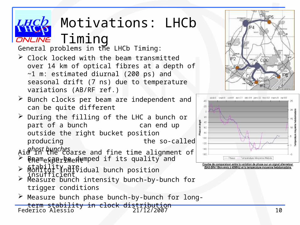
Federico Alessio 21/12/2007 10
Motivations: LHCb Timing
Aid in the coarse and fine time alignment of the experiment
Monitor individual bunch position Measure bunch intensity bunch-by-bunch for trigger
conditions Measure bunch phase bunch-by-bunch for long-term
stability in clock distribution
General problems in the LHCb Timing: Clock locked with the beam transmitted over 14
km of optical fibres at a depth of ~1 m: estimated diurnal (200 ps) and seasonal drift (7 ns) due to temperature variations (AB/RF ref.)
Bunch clocks per beam are independent and can be quite different
During the filling of the LHC a bunch or part of a bunch can end up outside the right bucket position producing the so-called ghost bunches
Beam can be dumped if its quality and stability are insufficient

Federico Alessio 21/12/2007 11
Solution: BPIM + RF2TTC
Proposal of a complete system to monitor, control, and time align LHCb experiment
Gives a clear structure of the beam injected taking the bipolar pulse coming from BPTX
Determines the position of the orbit locally and monitors the clock phase with respect to the bunch passing through the detector
Determines the exact trigger conditions for sampling events in the detector and determines the exact trigger conditions for significant events or not, checking whether the detector samples a bunch with protons or an empty bunch
Produces a relative measure of the intensities of bunches
Produces an empty crossing veto for the sampled events whenever a bunch is absent in the expected location
Searches for ghost bunches
Gives instantaneous information about the presence/absence of beam
Beam Phase and Intensity Monitor
RF2TTC System
Distributes the Bunch clocks and Orbit clocks to all the ODINs and therefore to all the FEE of each sub-detector
Able to convert, clean, synchronize and select the clocks for the experiment
Fine and coarse adjustments on the clock signals
Monitoring and controlling performed using a user-friendly GUI interface via the Experimental Control
System (ECS)

Federico Alessio 21/12/2007 12
In depth: specifications of BPIM
The 1st prototype
• Developing custom made acquisition board:– 6U VME, one per beam– Online analysis of a bipolar pulse: FWHM 1 ns at 40 MHz,
±5Vmax processing amplitude (onboard attenuator for higher pulses)
– Measure time between bunch arrivals and LHC bunch clock locally
• Bunch-by-bunch for a full LHC turn filled in FIFO • Triggered via controls interface• <100 ps precision and averaging phase as a function
of bunch crossing– Measure continuously bunch intensities bunch-by-bunch
• 12-bit resolution by integrating pulse per bunch• Output intensity on front-panel at 40 MHz (8/4-bit
resolution)• Triggered via controls interface, fill in FIFO with
intensities for full turn• Intensity per bunch as a function of bunch crossing
– Readout and control via Experiment Control System, CCPC based interface and VME alternatively
– Interfaced directly to LHCb Timing and Fast Control system
– Data processing on FPGA

Federico Alessio 21/12/2007 13
MAIN FPGA
LVDSDrivers
BX InfoGP outputs
ADC
TDC
Integrator+
Rectifier(positive)
Rectifier(negative)
FPGA
AttenuatorAnalogbuffer
Beam
Threshold comparator
Zero-crossingcomparator
ThresholdDAC
FPGA
Delay
PECLF/F
Data
Clock
Delay
Reset
Dis
char
ge
Sample
Leveladapter
Bunchclock Programmable
delay
FPGA Clockfanout
DelayOne-shot
LVPECL/PECL
8:1 Divider
LVPECL/PECL
LVPECL/PECL
LVPECL/PECL
2:1 Divider
One-shot
Start
Stop
FIFOPhase
FIFOIntensity
Local Bus
VME interface (FPGA)
Drivers
Glue Card
Credit Card PC
VME Bus
EthernetOrbit Level
adapter
In depth: overview of the board
6 logical blocks:- Intensity measurement chain- Phase measurement chain- Clock distribution - Digital processing and data accumulation- I/O interfaces- Board control via ECS
Every block has been tested and adjusted, and all blocks are working! The first prototype has been tested extensively in laboratory and in two test beams in the SPS.A second prototype has been submitted and is being produced. Will be tested during January/February with the dedicated Control System and installed in the LHCb cavern.

Federico Alessio 21/12/2007 14
In depth: debugging
The first prototype has been mounted and debugged in stages: a lot of modifications (thanks to the Mounting Workshop!) and understanding of the problems.
The analog chain is designed with current-feedback amplifiers: impressive slew rate and high gain-bandwith.
The stabilization of the rectifier chains has been a difficult task: the current feedback amplifiers are very unstable, but the best configuration has been found
New designs of the integrator have been implemented: improve stability, undershoot and baseline
Programmable attenuator fixed and constant-level-crossing method with programmable level (DAC)
Fixed Start and Stop signals for the TDC, still a problem with one mode of operation to be investigated with the manufactury (ACAM)
A lot of PECL – LVPECL and LVPECL – TTL translators implemented for improvements
Firmware written and implemented to control FIFOs for Intensity and Phase measurement
FIFOs are autonomous: each FIFO has its own RCLK, WCLK, OE, RENB, WENBThe board has very satisfactory performance!
Federico Alessio 21/12/2007 15
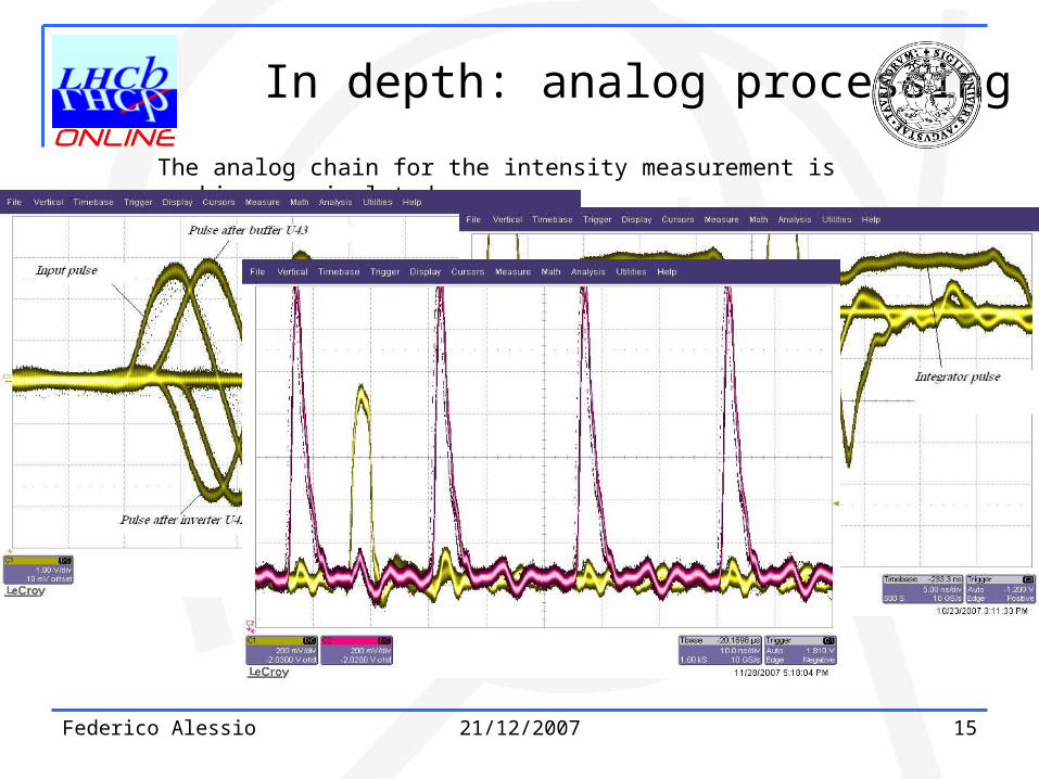
The analog chain for the intensity measurement is working as simulated
In depth: analog processing

Federico Alessio 21/12/2007 16
The board has extensively been tested in laboratory …
Linearization to be performed in the FPGA during the data processing
Understanding of a TDC problem in order to improve the confidence on the distribution
In depth: performance in the lab

Federico Alessio 21/12/2007 17
… and in the SPS with a LHC-like structure 72 bunches (in 3 groups) spaced by 25 ns.
Undershoot of the baseline after the sampling of the bunches to be understood
In depth: performance in the SPS

Federico Alessio 21/12/2007 18
Crate controller: CAEN USB to VME interface
6U VMEx64 crate
RF_Tx trasmitter: located in IP4, transmits the timing signals to the electronics
RF_Rx receiver: receives the timing signal from the RF_Tx
RF2TTC board: interface card between the receiver module and the TTC systems of the electronics
Clock Fanout: dual 1:18 ECL and 4 NIM
The LHC provides the Orbit clock and the Bunch clocks through the RF2TTC System
In depth: the RF2TTC system

Federico Alessio 21/12/2007 19
Main functionalities available in the board:
manual or automatic control of the board
selection of the clocks to feed to the TFC system. Bunch clock can be locked either on the Ref Clock or on one of the Bunch Clocks related to the beams while Orbit clock can be locked on one of the Orbit Clocks related to the beams
fine and coarse delay of the signals
definition of the length and period of the orbit pulses
orbit counters
general reset of the board
possibility to publish information sent from the accelerator
In depth: the RF2TTC system
Developed a Graphic User Interface to control the board via a Control Interface running on a dedicated crate processing unit

Federico Alessio 21/12/2007 20
Integrated Remote Control System for Electronic Boards…
In depth: the ECS
defines a generic data structure which allows to represent the state of all control and monitoring resources of a board of any type, and which has interfaces to the communication protocol and to the supervisory control and expert system
provides a simple and economical control communication protocol for the remote access mechanism to any board resource type independent of the bus type
provides a simple and economical mechanism which allows monitoring counters and status information by data registers subscription
provide a mapping between the logical or functional view and the hardware view of the boards provides a set of functions by which the control system can perform control actions and retrieve status information through the functional view of the system, either directed from a user interface or from an expert system

Federico Alessio 21/12/2007 21
Communication protocol based on the Distributed Information Management System
Based on a client/server paradigm: servers provide services to clients. It can run in the background updating information regularly: in the BPIM the server runs on the CCPC while in the RF2TTC it runs on the crate processing unit
The control of the electronics board is done through the industrial distributed SCADA system PVSS II from ETM
In depth: DIM & PVSS
Data Point
User Interfaces
Communication Protocol

Federico Alessio 21/12/2007 22
In depth: the ECS for the BPIM & RF2TTC
The DIM server runs on the CCPC and publishes services and commands
The PVSS API manager allows associating DIM commands and DIM services to the dynamic data structure in PVSS.
All the board resources are accessed via the PCI bus of the CCPC while the communication protocol over different buses is implemented in the glue cardOn each CCPC, the DIM server performs directly all the FPGA and the configuration
device programming, hardware configuration, data register access, and monitoring of each electronics board. It is independent of the board type and the organization of its resources. The DIM server is linked with library functions to operate over any type of busThe RF2TTC Control System works in the same way, but the DIM server runs on a dedicated crate processing unit and has been adapted for the TFC Control System.

Federico Alessio 21/12/2007 23
The control system for the RF2TTC is completely developed and fully working
In depth: the ECS for the BPIM & RF2TTC
The control system for the BPIM is under development and will be completed and tested with the second prototype of the board
Display Readings
Parameter Readings
Register Readings
UpdateRegister Structure
Parameter Settings
ReadWriteStructure
Register Settings
Control System
TranslationParam Regs
for FuncBlock
Display Settings
TranslationRegs Params
Automaticcomparison
GUI
SERVERRead->Set->Write->Read to hardware
Service(UpdateRegisters)
Command(ReadWriteRegisters)
Control Interface
Control network
Expert system
“Apply”
“Apply”

Federico Alessio 21/12/2007 24
The project is complete, fully working and is being installed and commissioned with the TFC system.
By means of the BPIM, the beam is monitored bunch-by-bunch in order to have a measurement of the phase of each single bunch clock with respect to the clock edge sent by the LHC. Moreover it is possible to measure the intensity of the beam bunch-by-bunch in order to trigger the acceptance/rejection of sampled events by the LHCb detector. A bunch of second prototypes of the board are already under production and will be completely tested during January/February. The control system is being developed and will be tested with the second prototype in order to have a complete system.
By means of the RF2TTC system, the clock sent to the TFC system is controlled. Fine adjustments can be performed on the clock in order to time align the experiment and to let the experiment sample events at the optimal point taking into account all the possible causes which can eventually shift the clock. The RF2TTC system has been installed in the LHCb cavern during December and the clock is directly fed into each of the ODINs used by the sub-detectors for the commissioning.
Conclusions

Federico Alessio 21/12/2007 25
The performance tests as well as the two test beams in the SPS gave successful results. The system will be then crucial for the timing of the LHCb, which can be monitored and controlled easily.
The control interface for the RF2TTC is completed, fully working and already tested. In January will be implemented in the Top Control System of LHCb and used for the commissioning of the detector.
The project has been presented to the LHCb and to the technical committee LEADE (LHC Experimental Accelerator Data Exchange Working Group) receiving extremely positive feedback and comments. The other LHC experiment showed their interests: ALICE will receive a second fully tested prototype board during March 2008 to be used for the time alignment of the ALICE detector.
The multitasking features allow the system to be used, adapted, and installed in any experiments similar to the ones at the LHC at CERN.
Conclusions
Grazie per l’attenzione