ferroelectric polymer nanostructures: fabrication
TRANSCRIPT
HAL Id: hal-01053228https://hal.archives-ouvertes.fr/hal-01053228
Submitted on 24 Nov 2014
HAL is a multi-disciplinary open accessarchive for the deposit and dissemination of sci-entific research documents, whether they are pub-lished or not. The documents may come fromteaching and research institutions in France orabroad, or from public or private research centers.
L’archive ouverte pluridisciplinaire HAL, estdestinée au dépôt et à la diffusion de documentsscientifiques de niveau recherche, publiés ou non,émanant des établissements d’enseignement et derecherche français ou étrangers, des laboratoirespublics ou privés.
Ferroelectric Polymer Nanostructures: Fabrication,Structural Characteristics and Performance Under
ConfinementD. Guo, F. Zeng, B. Dkhil
To cite this version:D. Guo, F. Zeng, B. Dkhil. Ferroelectric Polymer Nanostructures: Fabrication, Structural Character-istics and Performance Under Confinement. Journal of Nanoscience and Nanotechnology, AmericanScientific Publishers, 2014, 14, pp.2086-2100. �10.1166/jnn.2014.9272�. �hal-01053228�

Copyright © 2014 American Scientific PublishersAll rights reservedPrinted in the United States of America
ReviewJournal of
Nanoscience and NanotechnologyVol. 14, 2086–2100, 2014
www.aspbs.com/jnn
Ferroelectric Polymer Nanostructures:
Fabrication, Structural Characteristics and
Performance Under Confinement
Dong Guo1�∗, Fei Zeng2, and Brahim Dkhil3
1Institute of Acoustics, Chinese Academy of Sciences, Beijing 100190, China2Department of Materials Science and Engineering, Tsinghua University, Beijing 100086, China
3Laboratoire Structures, Propértiés et Modélisation des Solides, Ecole Centrale Paris, CNRS-UMR8580,
92290 Châtenay-Malabry, France
Ferroelectric polymers have recently attracted tremendous research interest due to their poten-
tial application in various emerging flexible devices. Nanostructured ferroelectric polymer materials,
such as nanorods, nanotube, and nanowires, are essential for miniaturization of the relevant elec-
tronic components. More importantly, their improved sensitivity and functionality may be used to
enhance the performance of existing devices or to develop and design new devices. In this arti-
cle, the recently developed methods for fabricating ferroelectric polymer nanostructures are briefly
reviewed. In particular, the distinct crystallization behaviors confined at the nanometer scale, the
nanoconfinement induced structural change, their influence on the physical properties of the ferro-
electric polymer nanostructures, and the possible underlying mechanisms are discussed.
Keywords: Ferroelectricity, PVDF, P(VDF-TrFE), Nanoconfinement, Polymer Crystallization.
CONTENTS1. Introduction . . . . . . . . . . . . . . . . . . . . . . . . . . . . . . . . . . . . . . . . 2086
2. Fabrication of Ferroelectric Polymer Nanostructures . . . . . . . . . 2088
2.1. ‘Top-Down’ Approaches . . . . . . . . . . . . . . . . . . . . . . . . . . 2088
2.2. Template Synthesis . . . . . . . . . . . . . . . . . . . . . . . . . . . . . . 2088
2.3. Electrospininng and Template Free Self-Organization . . . . 2091
3. Structural Change and Performance Under Nanoconfinement . . 2092
3.1. Nanoconfinement Effect in Monopolymer PVDF . . . . . . . . 2093
3.2. Nanoconfinement Effect in Copolymer P(VDF-TrFE) . . . . 2093
3.3. Discussion of the Common Features
Under Nanoconfinement . . . . . . . . . . . . . . . . . . . . . . . . . . . 2095
3.4. Performance of Other Ferroelectric
Polymers Under Nanoconfinement . . . . . . . . . . . . . . . . . . . 2096
4. Influence of Nanoconfinement on the Curie Transition
and Polarization Switching Behaviors . . . . . . . . . . . . . . . . . . . . 2097
5. Summary . . . . . . . . . . . . . . . . . . . . . . . . . . . . . . . . . . . . . . . . . . 2099
Acknowledgments . . . . . . . . . . . . . . . . . . . . . . . . . . . . . . . . . . . 2099
References and Notes . . . . . . . . . . . . . . . . . . . . . . . . . . . . . . . . 2099
1. INTRODUCTIONSince the discovery of ferroelectrics by Valasek in 1920,
significant theoretical and experimental advances have
∗Author to whom correspondence should be addressed.
been made in this fascinating field. Owing to the reversiblepolarization and the strong piezoelectric and pyroelec-tric effects, ferroelectric materials have been developedfor a broad range of applications, including sensing andactuation,1�2 data storage,3 energy harvesting4�5 electro-optics,6�7 and electrocalorics.8�9 Ferroelectrics may beclassified into two major groups: inorganic (oxides andnon-oxides) and organic (molecular crystals, liquid crys-tals and polymers) ones. Inorganic ferroelectrics include alarge number of oxides and non-oxides, among which theoxides with the perovskite structure in the form of ceram-ics are the predominant ones that have been used in variousdevices.10 In comparison, organic materials that displayferroelectric behaviors are mainly limited to a few types ofpolymers, including monopolymer poly(vinylidene difluo-ride) (PVDF), some VDF-containing fluorinated copoly-mers, certain odd-numbered polyamides such as Nylon 7and Nylon 11,11�12 and blends thereof.13�14 Among theseferroelectric polymers, only PVDF and the copolymer ofvinylidene fluoride and trifluoroethylene [P(VDF-TrFE)]have been used significantly so far.1�15 In order to dis-play ferroelectric behaviors, the chains of the ferroelectric
2086 J. Nanosci. Nanotechnol. 2014, Vol. 14, No. 2 1533-4880/2014/14/2086/015 doi:10.1166/jnn.2014.9272
Guo et al. Ferroelectric Polymer Nanostructures: Fabrication, Structural Characteristics and Performance Under Confinement
polymers must be able to crystallize in a manner in which
the molecular dipoles do not cancel out. As a result, only
the polar � and � phases are ferroelectrics. Relative to
inorganic ferroelectrics, ferroelectric polymers show low
spontaneous polarization, low phase transition temperature
(Curie temperature, Tc) and usually a small dielectric con-
stant. However, their special characteristics like high elec-
tric breakdown field, light weight, flexibility and ease of
processing, etc., make them very promising for specific
applications. Particularly, the rapid development of flexi-
ble electronics industry in the last two decades has spurred
tremendous research interest on ferroelectric polymers.
The ever-increasing demand for device miniaturiza-
tion requires the fabrication of ordered ferroelectric poly-
mer nanostructures. Compared to inorganic ferroelectrics,
ferroelectric polymers show much more complicated
structural characteristics such as the many possible
configurations and conformations in addition to the par-
tial crystallinity. In the latter, it is generally accepted
that the ferroelectricity originates from ordered packing
of F–C–H molecular dipoles in the crystalline region.16�17
Dong Guo was born in 1974. He received the Ph.D. degree in Department of Materials
Science and Engineering in Tsinghua University, Beijing, China, in 2003. From 2003 to
2007, he worked continuously on organic thin films of both small molecules and polymer
and relevant devices in Tokyo Institute of Technology (JST postdoctoral researcher), the
University of Tokyo (JSPS foreigner postdoctoral researcher), and National Institute for
Materials Science (NIMS) in Japan. From 2007 to 2009, he was a foreigner scientist at
the Ceramics Laboratory of Swiss Federal Institute of Technology at Lausanne (EPFL).
In 2010, he joined in institute of Acoustics, Chinese Academy of Science, as a ‘Hun-
dred Talents Program’ Professor. He is the leader of the ‘Functional Materials Group’ of
the institute, and the current research of his group is focused on various piezoelectric,
ferroelectric and semiconductive materials, and their application in various devices.
Fei Zeng received his Ph.D. degree from Tsinghua University, China, in 2002. He is now
an associate professor in School of Materials Science, Tsinghua University, China. His
research is focused on the growth of organic and inorganic thin films, their electric prop-
erties, and new memory phenomena, such as neuromorphic with simple polymer memory
devices. He has published over 100 research articles in the past 10 years.
Brahim Dkhil received a Ph.D. in Materials Science from University of Orsay, France and
is currently working at Structures, Properties and Modelling of Solids laborat ory at Ecole
Centrale Paris, France. He is the group leader of the “Advanced Ferroics” group aiming
at better understanding the microscopic mechanisms and the couplings at the origin of the
properties of these materials. His current research focuses on ferroel ectric, relaxor and
multiferroic materials and he has over 130 publications.
As a consequence, the growth mechanism of ferroelectric
polymers crystals is strikingly different from those of inor-
ganic ones, and this in turn leads to their different physical
properties. For nanostructured polymers, the situation is
further complicated by the confined dimension.18�19 Details
about the microstructure evolution and size dependent
performance of ferroelectric polymers are still not fully
understood.20�21 On the other hand, unexpected behav-
iors under geometrical confinement at the nanometer scale
(nanoconfinement) may lead to special functionalities that
can be used to enhance the performance of existing devices
or to develop and design novel devices.22�23 Perhaps due to
these reasons, nanostructured ferroelectric polymers have
been attracting increasing research interest in recent years.
There are excellent reviews on organic ferroelectrics15�24
and inorganic ferroelectric nanostructures,6�25 while a
review about the fabrication and performance of ferroelec-
tric polymer nanostructures seems still not available up
to now. Here we first provide an overview on the meth-
ods developed over the last decade for fabricating ferro-
electric polymer nanostructures, mainly those of PVDF
J. Nanosci. Nanotechnol. 14, 2086–2100, 2014 2087

Ferroelectric Polymer Nanostructures: Fabrication, Structural Characteristics and Performance Under Confinement Guo et al.
and P(VDF-TrFE). Following that, we focus the discussionon the nanoconfinement induced structural characteristicsand physical property change of the ferroelectric poly-mers. Furthermore, the possible underlying mechanismsare discussed.
2. FABRICATION OF FERROELECTRICPOLYMER NANOSTRUCTURES
There are basically two approaches for fabricating nano-structures: ‘bottom-up’ and ‘top-down.’ The former refersto the build-up of nanomaterials starting from the atomicor molecular level.26 The latter refers to successive cuttingof a bulk material to get ordered arrays of nanostructuresby using higher-energy radiation or beams such as laser,X-ray from synchrotron radiation source and focused ionbeam, etc.27 Both approaches have been used for fabri-cating ferroelectric polymer nanostructures. In general, themethods are similar to those used for fabricating othertypes of polymer nanostructures. As the functionality ofthe ferroelectric polymer originates from the alignmentof molecular dipoles in the lager number of connectedmonomers, molecular packing order and dipole orientationare important factors that need to be considered duringprocessing.16�17 The two types of methods will be sequen-tially discussed in the following Sections 2.1 and 2.2.Some other rarely used methods will also be discussed inSection 2.3.
2.1. ‘Top-Down’ Approaches
2.1.1. Conventional ‘Top-Down’ Approaches
Early work for the fabrication of ferroelectric polymermicro or nanostructures was performed using conventional‘top-down’ approaches, and only very few have beenreported so far. Nanoscale fabrication of various fluori-nated polymers has been demonstrated by direct focusedion beam (FIB) etching without any mask.28 The lim-ited data indicated that the etching rates of perfluori-nated polymers were about 500–1000 times higher thanthose of partially fluorinated polymers like PVDF, whichwas attributed to the limited decomposition of macro-molecules because of the formation of network and con-jugated double bonds in partially fluorinated polymers.X-rays from a synchrotron radiation source has also beenused to photo etch PVDF29 and P(VDF-TrFE)30 thin filmsvia photodegradation, and polymer patterns in the microm-eter scale have been fabricated with a Si membrane mask.However, the need of complicated facilities, the low fab-rication rate and the defects or damages caused duringprocessing seriously limit the application of this kind ofmethods.
2.1.2. Nanoimprint Lithography
Nanoimprint lithography (NIL), also referred to ashot embossing, is a simple nanolithography processfor fabricating high resolution nanoscale patterns by
mechanical deformation of imprint resist and subsequentprocessing.31�32 The imprint resist is typically a monomeror polymer formulation that can be cured by heat or UVlight during the imprinting. The imprinting mold is gen-erally prepared by normal nanoprocessing techniques suchas electron beam lithography or reactive ion etching. NILis capable of producing a variety of highly ordered ferro-electric nanostructures. A problem of this method is thedifficulty to fabricate nanostructures with high aspect ratiobecause of the adhesion caused by the high contact areabetween the mold and the polymer. Surface modificationsuch as self-assembled monolayer and plasma treatmentare therefore used for effective release of the polymernanostructures.33
Early work about application of imprinting to fluori-nated polymers was conducted to pattern �-phase PVDF,which is not a ferroelectric.34 Another study indicatedthat pressure could induce the formation of ferroelectric�-phase PVDF.35 Imprinting of thin PVDF films withpolydimethylsiloxane (PDMS) mold at a pressure of hun-dreds kPa at elevated temperatures produced micropatternsin which the regions compressed by the molds were trans-formed into the ferroelectric phase, while the obtainedpatterns were in sub-micrometer scale. In contrast topure PVDF, ferroelectric phase of the copolymer P(VDF-TrFE) can be directly formed in many manners. Zhangand coworkers36 applied imprinting to P(VDF-TrFE) films,which showed well shaped ferroelectric hysteresis loops,and a good correlation was observed between the rem-nant polarization and the surface potential of the imprintedfilms.
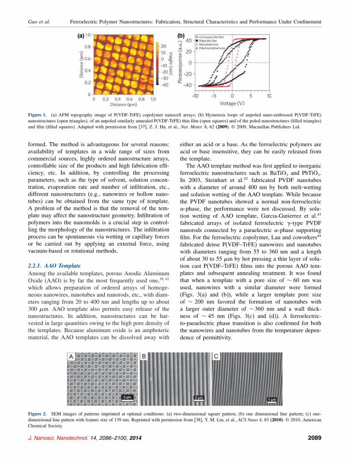
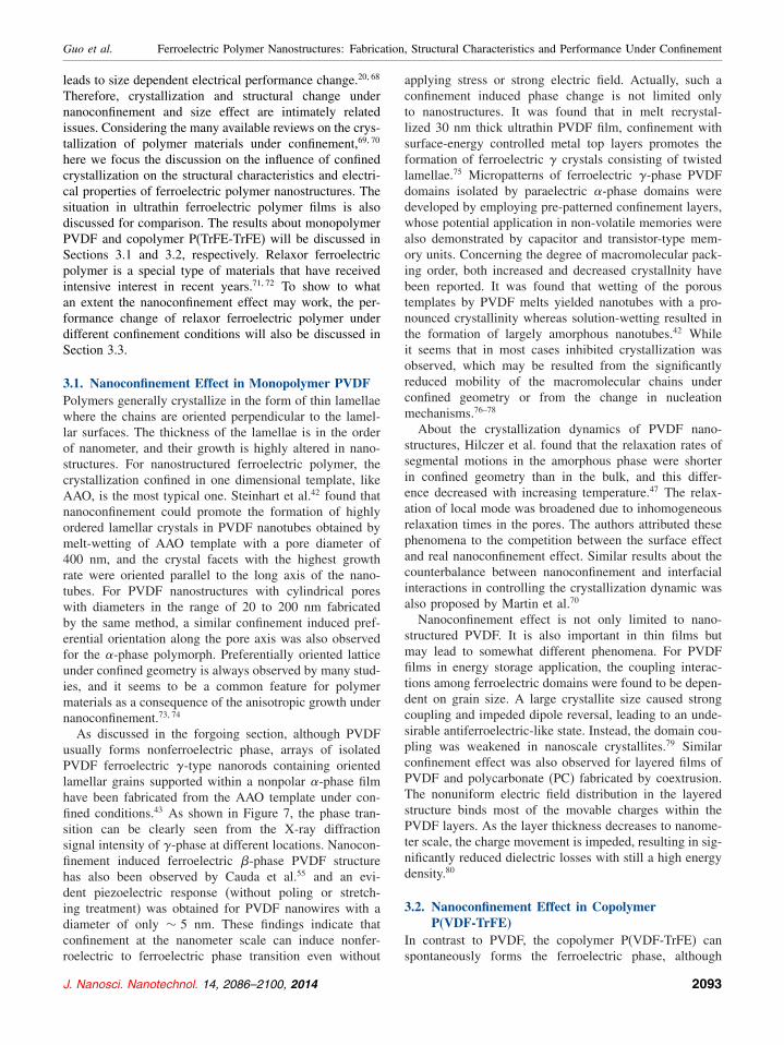
A later study demonstrated the possibility to getnanocell arrays (Fig. 1) with preferentially orientatedmolecular dipoles and significantly eliminated structuraldefects by using the NIL method with optimized process-ing conditions.37 The improved structure quality enableslow-voltage operation and uniform polarization switch-ing. A more recent study developed a rapid nanoimprint-ing process to pattern large area of P(VDF-TrFE) regulararrays with a much shorter imprinting time than the normalNIL procedure.38 As shown in Figure 2, the reported small-est feature size of the imprinted pattern is 139 nm. Goodferroelectric properties and piezoresponse for the patternsobtained under the optimal imprinting conditions withoutannealing treatment have also been achieved.
2.2. Template Synthesis
‘Template synthesis’ is a well established ‘bottom-up’approach in fabricating various types of nanostructuredmaterials, and it is also a widely used strategy in mak-ing ferroelectric polymer nanostructures.39�40 The methodconsists of two main steps: nanomolding via infiltration ofpolymer solution or melt into the nanosized channels orporesin a non-reactive template and subsequent removalof the template. One dimensional polymer nanowires, rodsand tubes with an inverse geometry of the template can be
2088 J. Nanosci. Nanotechnol. 14, 2086–2100, 2014
Guo et al. Ferroelectric Polymer Nanostructures: Fabrication, Structural Characteristics and Performance Under Confinement
Figure 1. (a) AFM topography image of P(VDF-TrFE) copolymer nanocell arrays; (b) Hysteresis loops of unpoled nano-embossed P(VDF-TrFE)
nanostructures (open triangles), of an unpoled similarly annealed P(VDF-TrFE) thin film (open squares) and of the poled nanostructures (filled triangles)
and film (filled squares). Adapted with permission from [37], Z. J. Hu, et al., Nat. Mater. 8, 62 (2009). © 2009, Macmillan Publishers Ltd.
formed. The method is advantageous for several reasons:availability of templates in a wide range of sizes fromcommercial sources, highly ordered nanostructure arrays,controllable size of the products and high fabrication effi-ciency, etc. In addition, by controlling the processingparameters, such as the type of solvent, solution concen-tration, evaporation rate and number of infiltration, etc.,different nanostructures (e.g., nanowires or hollow nano-tubes) can be obtained from the same type of template.A problem of the method is that the removal of the tem-plate may affect the nanostructure geometry. Infiltration ofpolymers into the nanomolds is a crucial step in control-ling the morphology of the nanostructures. The infiltrationprocess can be spontaneous via wetting or capillary forcesor be carried out by applying an external force, usingvacuum-based or rotational methods.
2.2.1. AAO Template
Among the available templates, porous Anodic AluminumOxide (AAO) is by far the most frequently used one,39�41
which allows preparation of ordered arrays of homoge-neous nanowires, nanotubes and nanorods, etc., with diam-eters ranging from 20 to 400 nm and lengths up to about300 �m. AAO template also permits easy release of thenanostructures. In addition, nanostructures can be har-vested in large quantities owing to the high pore density ofthe templates. Because aluminum oxide is an amphotericmaterial, the AAO templates can be dissolved away with
Figure 2. SEM images of patterns imprinted at optimal conditions: (a) two-dimensional square pattern; (b) one dimensional line pattern; (c) one-
dimensional line pattern with feature size of 139 nm. Reprinted with permission from [38], Y. M. Liu, et al., ACS Nano 4, 83 (2010). © 2010, American
Chemical Society.
either an acid or a base. As the ferroelectric polymers are
acid or base insensitive, they can be easily released from
the template.
The AAO template method was first applied to inorganic
ferroelectric nanostructures such as BaTiO3 and PbTiO3.
In 2003, Steinhart et al�42 fabricated PVDF nanotubes
with a diameter of around 400 nm by both melt-wetting
and solution wetting of the AAO template. While because
the PVDF nanotubes showed a normal non-ferroelectric
�-phase, the performance were not discussed. By solu-
tion wetting of AAO template, Garcıa-Gutierrez et al.43
fabricated arrays of isolated ferroelectric �-type PVDF
nanorods connected by a paraelectric �-phase supporting
film. For the ferroelectric copolymer, Lau and coworkers44
fabricated dense P(VDF–TrFE) nanowires and nanotubes
with diameters ranging from 55 to 360 nm and a length
of about 30 to 55 �m by hot pressing a thin layer of solu-
tion cast P(VDF–TrFE) films into the porous AAO tem-
plates and subsequent annealing treatment. It was found
that when a template with a pore size of ∼ 60 nm was
used, nanowires with a similar diameter were formed
(Figs. 3(a) and (b)), while a larger template pore size
of ∼ 200 nm favored the formation of nanotubes with
a larger outer diameter of ∼360 nm and a wall thick-
ness of ∼ 45 nm (Figs. 3(c) and (d)). A ferroelectric-
to-paraelectric phase transition is also confirmed for both
the nanowires and nanotubes from the temperature depen-
dence of permittivity.
J. Nanosci. Nanotechnol. 14, 2086–2100, 2014 2089

Ferroelectric Polymer Nanostructures: Fabrication, Structural Characteristics and Performance Under Confinement Guo et al.
Figure 3. (a) and (b) are the SEM images of the P(VDF-TrFE) nanowires; (c) and (d) are the SEM images of the P(VDF-TrFE) nanotubes. Reprinted
with permission from [44], S. T. Lau, et al., Mater. Lett. 60, 2357 (2006). © 2006, Elsevier B.V.
Using the AAO template, Li et al.45 fabricated arrays of
special P(VDF-TrFE) nanotubes being sealed at one end
and linked at the open end. The authors deposited silver
electrodes on both the outer and inner sides of the nano-
tubes by electroless plating. In such a structure, electrical
short-circuit between the inner and outer electrodes can
be avoided. A much larger capacitance due to the greatly
enlarged contact area between the electrodes and the poly-
mer dielectric was reported for the nanotube array. Similar
method was also used to fabricate a composite consisting
of P(VDF-TrFE) nanotubes and an organic semiconduc-
tor filler.46 The composite showed a large dielectric con-
stant, which was attributed to the significantly enhanced
interface polarization between the fillers and the polymer
matrix. There are also many other works about fabrica-
tion of PVDF or P(VDF-TrFE) nanostructures using the
similar template,47–52 which will not be discussed in detail
here because of the similarity in processing and feature
sizes, etc.
2.2.2. Silicon Based Template
It was found that the AAO template might cause entan-
glement and leaning of the nanostructures due to the low
stiffness and softness of the polymers. To get well-aligned
ferroelectric polymer nanorod arrays, SiO2 templates pre-
pared by a semiconductor fabrication process were also
tried.53 In this method, after infiltration of P(VDF–TrFE)
solution into the template, the sample was dried in a vac-
uum oven at room temperature. The results demonstrated
that when the template removal and crystallization of the
polymer were carried out simultaneously in hot etchant
at around 100 �C, well-aligned arrays of one-dimensional
nanorods with a diameter of ∼120 nm with still a high
aspect ratio was obtained (Fig. 4). Unlike the AAO tem-
plates, however, a problem of this method is that infiltration
of P(VDF–TrFE) solution can be inhibited due to air in the
holes because the bottom of the SiO2 templates is blocked.
A vertically oriented P(VDF-TrFE) ‘nanograss’ struc-
ture with a nanopillar diameter around 20 nm and with
still a high aspect ratio has been imprinted using a sili-
con nanograss mold.54 Through evaporation-induced self-
assembly of silica-precursor solution in the channels of
AAO template, Cauda et al.55 synthesized columnar meso-
porous silica embedded in AAO membrane templates.
Such a structure may be seen as a composite template.
By wet-impregnation of the hierarchical host membrane
template with PVDF and P(VDF-TrFE) solution and sub-
sequent thermal treatment, the authors fabricated ferroelec-
tric polymer nanowires with a diameter of around 5 to
10 nm and a length up to 60 �m (Fig. 5). These results
indicate that Si based template may be used to fabricate
one-dimensional ferroelectric polymer nanostructures with
a smaller feature size compared to those made from AAO
templates.
2090 J. Nanosci. Nanotechnol. 14, 2086–2100, 2014

Guo et al. Ferroelectric Polymer Nanostructures: Fabrication, Structural Characteristics and Performance Under Confinement
Figure 4. (a) Schematic process diagram of nanostructure fabrication; (b) and (c) are the SEM images of the P(VDF-TrFE) nanorod arrays. Adapted
with permission from [53], Oh, et al., Adv. Mater. 24, 5708 (2012). © 2012, Wiley-VCH Verlag GmbH & Co. KGaA, Weinheim.
2.3. Electrospininng and Template Free
Self-Organization
Electrospinning is a highly suitable technique for the fab-
rication of high aspect ratio polymer nanofibers, despite its
Figure 5. (a) Transmission electron microscopy (TEM) images of the plane-view of columnar mesoporous silica in AAO membranes; (b) PVDF rods
in AAO with a pore size of 10 nm; (c) AFM topology image of the array of PVDF nanowires distributed in AAO with a pore size of 10 nm; (d)
modulus of the piezoelectric coefficient d33 estimated by PFM of the nanowires shown in image (c). Adapted with permission from [55], V. Cauda,
et al., Chem. Mater. 240, 4215 (2012). © 2012, American Chemical Society.
difficulties to precisely control the fiber diameter and to
achieve diameters bellow 100 nm.56 PVDF usually forms
a non-ferroelectric phase, however, ferroelectric PVDF
nanofibers have been directly fabricated recently by using
J. Nanosci. Nanotechnol. 14, 2086–2100, 2014 2091

Ferroelectric Polymer Nanostructures: Fabrication, Structural Characteristics and Performance Under Confinement Guo et al.
near-field electrospinning, and a novel nanogenerator with
interesting mechanical stretch and electrical poling charac-
teristics has been reported.4 The strong electric fields and
stretching forces result in preferentially oriented dipoles in
the nanofiber crystals, and thus the nonpolar �-phase struc-
ture can be transformed into polar �-phase one. Moreover,
in this method poling is not needed to induce dipole ori-
entation, and the fibers can directly produce voltage and
current outputs when the substrate is stretched and released
repeatedly (Fig. 6). However, the reported diameters of
the as-spun ferroelectric nanofibers fabricated by this way
are in the micrometer scale. P(VDF-TrFE) nanofiber webs
with diameters of about 60–120 nm have also been pre-
pared by normal electrospinning.57 As the dipoles in the
nanofibers are preferentially oriented toward the thickness
direction of the nanoweb, enhanced performance was con-
sidered to be possible by stacking the nanofiber webs.
Among the ‘bottom-up’ approaches, self-assembly
based template free method is one of the simplest routes
for preparing nanostructures.26�58–60 However, a significant
problem is that the material or its precursor must have
the intrinsic ability for self-organizing, which is driven
by interactions that can minimize the overall energy of
the system.61 Although self-assembly has been success-
fully used for the synthesis of some specific organic nano-
structures with controllable patterns or geometries, the
spectrum of materials that can integrate polymer is still
limited,62�63 and up to now only very few studies have
been tried for ferroelectric polymers. Numerical simulation
based on phase field approach indicates that proper exter-
nal mechanism may trigger the formation of self-organized
Figure 6. (a) Schematic illustration of the nanogenerator fabrication process that combines near-field electrospinning, direct-writing, mechanical
stretching, and in situ electrical poling; (b) SEM image of a single PVDF fiber nanogenerator; (c) and (d) are the output voltage and output current
measured under repeated strain. Reprinted with permission from [4], C. Chang, et al., Nano Lett. 10, 726 (2010). © 2010, American Chemical Society.
P(VDF-TrFE) nanostructure patterns and regulate theirsize, morphology and distribution.64 A recent experimenthas demonstrated that P(VDF-TrFE) nanowire (with adiameter around 200 nm) patterns can be fabricated fromthe melt phase by confined crystallization without anytemplates.65 The large difference in the lateral and verti-cal amplitude signals of Piezoresponse Force Microscopy(PFM) also reveals an anisotropic piezoelectric responseof the nanowires because their dipoles are preferentiallyorientated parallel relative to the substrate. These stud-ies demonstrate the possibility of fabricating ferroelectricpolymer nanostructures via template free self-assembly.However, to fully realize the technological potential of themethod, problems like poor control over size and distribu-tion and irregular morphology of the nanostructures needto be resolved.
3. STRUCTURAL CHANGE ANDPERFORMANCE UNDERNANOCONFINEMENT
Nanostructured materials always show remarkabledeviations in properties compared to bulk materials. Thisis especially true for ferroelectric polymer. The growthor crystallization of polymer is a non-equilibrium processthat requires the cooperative movements of large numberof connected monomers.66�67 In polymer nanostructuresthe process is further complicated by the constrainedgeometry, and the resulting crystalline morphologiesare usually metastable. On the other hand, reduction indimension may cause significant change in the long andshort range ordering of molecular dipoles, which in turn
2092 J. Nanosci. Nanotechnol. 14, 2086–2100, 2014
Guo et al. Ferroelectric Polymer Nanostructures: Fabrication, Structural Characteristics and Performance Under Confinement
leads to size dependent electrical performance change.20�68
Therefore, crystallization and structural change undernanoconfinement and size effect are intimately relatedissues. Considering the many available reviews on the crys-tallization of polymer materials under confinement,69�70
here we focus the discussion on the influence of confinedcrystallization on the structural characteristics and electri-cal properties of ferroelectric polymer nanostructures. Thesituation in ultrathin ferroelectric polymer films is alsodiscussed for comparison. The results about monopolymerPVDF and copolymer P(TrFE-TrFE) will be discussed inSections 3.1 and 3.2, respectively. Relaxor ferroelectricpolymer is a special type of materials that have receivedintensive interest in recent years.71�72 To show to whatan extent the nanoconfinement effect may work, the per-formance change of relaxor ferroelectric polymer underdifferent confinement conditions will also be discussed inSection 3.3.
3.1. Nanoconfinement Effect in Monopolymer PVDF
Polymers generally crystallize in the form of thin lamellaewhere the chains are oriented perpendicular to the lamel-lar surfaces. The thickness of the lamellae is in the orderof nanometer, and their growth is highly altered in nano-structures. For nanostructured ferroelectric polymer, thecrystallization confined in one dimensional template, likeAAO, is the most typical one. Steinhart et al.42 found thatnanoconfinement could promote the formation of highlyordered lamellar crystals in PVDF nanotubes obtained bymelt-wetting of AAO template with a pore diameter of400 nm, and the crystal facets with the highest growthrate were oriented parallel to the long axis of the nano-tubes. For PVDF nanostructures with cylindrical poreswith diameters in the range of 20 to 200 nm fabricatedby the same method, a similar confinement induced pref-erential orientation along the pore axis was also observedfor the �-phase polymorph. Preferentially oriented latticeunder confined geometry is always observed by many stud-ies, and it seems to be a common feature for polymermaterials as a consequence of the anisotropic growth undernanoconfinement.73�74
As discussed in the forgoing section, although PVDFusually forms nonferroelectric phase, arrays of isolatedPVDF ferroelectric �-type nanorods containing orientedlamellar grains supported within a nonpolar �-phase filmhave been fabricated from the AAO template under con-fined conditions.43 As shown in Figure 7, the phase tran-sition can be clearly seen from the X-ray diffractionsignal intensity of �-phase at different locations. Nanocon-finement induced ferroelectric �-phase PVDF structurehas also been observed by Cauda et al.55 and an evi-dent piezoelectric response (without poling or stretch-ing treatment) was obtained for PVDF nanowires with adiameter of only ∼ 5 nm. These findings indicate thatconfinement at the nanometer scale can induce nonfer-roelectric to ferroelectric phase transition even without
applying stress or strong electric field. Actually, such aconfinement induced phase change is not limited onlyto nanostructures. It was found that in melt recrystal-lized 30 nm thick ultrathin PVDF film, confinement withsurface-energy controlled metal top layers promotes theformation of ferroelectric � crystals consisting of twistedlamellae.75 Micropatterns of ferroelectric �-phase PVDFdomains isolated by paraelectric �-phase domains weredeveloped by employing pre-patterned confinement layers,whose potential application in non-volatile memories werealso demonstrated by capacitor and transistor-type mem-ory units. Concerning the degree of macromolecular pack-ing order, both increased and decreased crystallnity havebeen reported. It was found that wetting of the poroustemplates by PVDF melts yielded nanotubes with a pro-nounced crystallinity whereas solution-wetting resulted inthe formation of largely amorphous nanotubes.42 Whileit seems that in most cases inhibited crystallization wasobserved, which may be resulted from the significantlyreduced mobility of the macromolecular chains underconfined geometry or from the change in nucleationmechanisms.76–78
About the crystallization dynamics of PVDF nano-structures, Hilczer et al. found that the relaxation rates ofsegmental motions in the amorphous phase were shorterin confined geometry than in the bulk, and this differ-ence decreased with increasing temperature.47 The relax-ation of local mode was broadened due to inhomogeneousrelaxation times in the pores. The authors attributed thesephenomena to the competition between the surface effectand real nanoconfinement effect. Similar results about thecounterbalance between nanoconfinement and interfacialinteractions in controlling the crystallization dynamic wasalso proposed by Martin et al.70
Nanoconfinement effect is not only limited to nano-structured PVDF. It is also important in thin films butmay lead to somewhat different phenomena. For PVDFfilms in energy storage application, the coupling interac-tions among ferroelectric domains were found to be depen-dent on grain size. A large crystallite size caused strongcoupling and impeded dipole reversal, leading to an unde-sirable antiferroelectric-like state. Instead, the domain cou-pling was weakened in nanoscale crystallites.79 Similarconfinement effect was also observed for layered films ofPVDF and polycarbonate (PC) fabricated by coextrusion.The nonuniform electric field distribution in the layeredstructure binds most of the movable charges within thePVDF layers. As the layer thickness decreases to nanome-ter scale, the charge movement is impeded, resulting in sig-nificantly reduced dielectric losses with still a high energydensity.80
3.2. Nanoconfinement Effect in Copolymer
P(VDF-TrFE)
In contrast to PVDF, the copolymer P(VDF-TrFE) canspontaneously forms the ferroelectric phase, although
J. Nanosci. Nanotechnol. 14, 2086–2100, 2014 2093

Ferroelectric Polymer Nanostructures: Fabrication, Structural Characteristics and Performance Under Confinement Guo et al.
Figure 7. (a) SEM images showing the side and top (inset) views of the PVDF nanorod morphology; (b) cross section of a fractured sample, the
inset is a magnified image of the interface between the residual PVDF film (right) and the nanorod array (left); (c) Spatial evolution of degree of
crystallinity from the residual polymer film (bulk) to the nanorod array; (d) Spatial evolution of the �-phase fraction; (e) FWHM of the 020 reflection
indicating the improved orientation. Adapted with permission from [43], M. C. Garcıa-Gutierrez, et al., Nano Lett. 10, 1472 (2010). © 2010, American
Chemical Society.
the paraelectric phase may also appears. So far most
studies about the confinement effect in the copolymer
have been focused on its thin films (generally referred
to as ‘finite size effect’), whose ferroelectricity gener-
ally drops markedly when the thickness is less than
50–100 nm.20�67�81–83 In P(VDF-TrFE) nanostructures,
however, the size dependent ferroelectric or piezoelectric
performance is rather different and by far less investigated.
For P(VDF-TrFE) nanorods confined within AAO tem-
plates, significant deviation from bulk behavior was
observed when the pore diameter is less than 40 nm,
and nanoconfinement was found to be able to largely
enhance the formation of ferroelectric phase (as simi-
lar to the phenomena in PVDF), which was explained
by the high molecule packing density of the ferro-
electric phase oriented crystallization under confinement
geometry.50 Consequently, a better piezoelectric response
was expected, and the melting temperature of the nanorods
also decreased with decreasing pore diameter. Investi-
gation on the formation of P(VDF-TrFE) nanostructures
via melt wetting of AAO template indicated that, cys-
tallization within the template during cooling led to the
transition of highly oriented paraelectric phase to ferro-
electric phase with a lower degree of orientation. In the
final sample the chains are preferentially oriented per-
pendicular to the long axis of the nanopores, and the
size of the crystalline domains is also restricted by the
nanopores.49 P(VDF-TrFE) nanostructures consisting of
nanorod arrays and residual film fabricated by solution
wetting of AAO template have been studied by using scan-
ning X-ray microdiffraction with synchrotron light. A spa-
tial evolution of polymorphs from a mixture of paraelectric
and ferroelectric crystals in the film to a pure ferroelec-
tric phase nanorod arrays was observed. In contrast, only
2094 J. Nanosci. Nanotechnol. 14, 2086–2100, 2014

Guo et al. Ferroelectric Polymer Nanostructures: Fabrication, Structural Characteristics and Performance Under Confinement
ferroelectric phase was obtained in the whole structure
fabricated by melt wetting of AAO. A decreased macro-
molecular packing order under nanoconfinement caused a
crystallinity distribution gradient.84
Advantageous nanoconfinement effect has also been
demonstrated by using prototype sensors.48 By comparing
the structure and electromechanical characteristics of one-
dimensional nanowires in 200-nm channel AAO and two
dimensional films of P(VDF-TrFE) without electric poling,
Canavese et al. observed improved piezoelectric response
under nanoconfinement. Furthermore, they fabricated flexi-
ble tactile sensors and bendable energy harvesters using dif-
ferent polymeric structures and showed that the nanowire
sample under confined conditions could generate higher
amount of charge compared to that of the thin film sample.
The improved sensitivity was attributed to the better spa-
tial arrangement of macromolecular chains, the enhanced
� crystalline structure with the favorable orientation of the
polarization axis under nanoconfinement.
For one dimensional grating P(VDF-TrFE) nano-
structure with a depth of 120 nm and a width of 120 nm
fabricated by NIL, it was found that the confinement
imposed by the wall trenches of the grating promoted the
formation of smaller edge-on oriented lamellar crystals,
resulting in ferroelectric domains with a size of one order
of magnitude smaller compared to those of the domains
in two dimensional films. In such a grating nanostructure
the problem caused by uncontrolled large extension of
ferroelectric signal over needlelike crystals in films was
expected to be resolved, and a large information density of
about 0.5 T bit per in Ref. [2] was calculated.85 Another
report on P(VDF-TrFE) nanocells with a thickness of
Figure 8. (a) Temperature dependence of the real part of the linear dielectric constant �′ for unpoled and poled P(VDF-TrFE) layers with different
thicknesses, where the solid lines represent the data of the poled samples; (b) Curie plots for unpoled P(VDF-TrFE) layers; the Tc for each sample can
be estimated from the intersection of the two straight dashed lines. Adapted with permission from [86], Urayama, et al., Macromolecules. 33, 8269
(2000). © 2000, American Chemical Society.
∼ 80 nm fabricated by NIL indicated that, when themold cavities were narrow and deep enough so that thecrystallization propagation in the isolated nanocells wasprevented, the molecular backbones were preferentiallyoriented parallel relative to the substrate.37 Such a ‘com-plete confinement’ was considered to be responsible forthe improved ferroelectric performance, as revealed by theloops shown in Figure 1(b). Also, obvious ferroelectric-ity in P(VDF-TrFE) nanotubes with a wall thickness ofa few tens of nanometers has been observed.46 For theP(VDF-TrFE) copolymer ‘nanograss’ structure with a fur-ther decreased lateral size of around 20 nm mentionedin the Subsection 2.2.2,54 a piezoelectricity about severaltimes larger than that of the flat film as evaluated by PFMamplitude signal was reported.
3.3. Discussion of the Common Features
Under Nanoconfinement
For ease of comparison, a summary of the structuralcharacteristics and property change under confinement ofvarious nanostructures (ultrathin films) of the two typi-cal ferroelectric polymers fabricated by different approach-es is given in Table I. From the many results it seemsthat, despite the inhibited crystallization, nanoconfinementcan improve the ferroelectric performance in the P(VDF-TrFE). Therefore, several common features may be gener-alized for the ferroelectric polymers:(1) nanoconfinement usually leads to preferential orien-tation of the polymer chains, although the crystallizationmay be inhibited;(2) nanoconfinement may promote the formation of ferro-electric phase in both the monopolymer and copolymer;
J. Nanosci. Nanotechnol. 14, 2086–2100, 2014 2095

Ferroelectric Polymer Nanostructures: Fabrication, Structural Characteristics and Performance Under Confinement Guo et al.
Table I. Summary of the structural characteristics and property change under confinement of nanostructures (ultrathin films) of the two polymers
fabricated by different approaches.
Material Fabrication approach Feature size Structural change Tc change Refs.
PVDF film ∼100 nm (thickness) �-to �-phase [35]
PVDF nanotubes AAO template ∼400 nm (diameter) Improved crystallinity [42]
PVDF nanorods AAO template 150–200 nm (diameter) �-to �-phase [43, 84]
PVDF nanorods AAO template 20–200 nm (diameter) Reduced crystallinity [47]
PVDF nanowires Mesoporous silica in
AAO
∼5–10 nm (diameter) �-to �-phase [55]
PVDF film 30 nm (thickness) �-to �-phase [75]
P(VDF-TrFE) nanocell
arrays and nanogratings
Microimprinting ∼2 �m (width) [36]
P(VDF-TrFE) nanocell
arrays
NIL 80 nm (height)×140 nm
(width)
Improved crystallinity [37]
P(VDF-TrFE) regular arrays NIL ∼139 nm (width) [38]
P(VDF-TrFE) nanowires AAO template 55–360 nm (diameter) [44]
P(VDF-TrFE) nanotubes AAO template 250–300 nm (diameter) [45]
P(VDF-TrFE) nanotubes and
composite nanotubes
AAO template 50–150 nm (diameter) Reduced crystallinity [46]
P(VDF-TrFE) nanowires AAO template ∼200 nm (diameter) Improved crystallinity [48]
P(VDF-TrFE) nanorods and
nanotubes
AAO template 35–400 nm (diameter) Reduced crystallinity Unaltered [49]
P(VDF-TrFE) nanorods AAO template 15–200 nm (diameter) Improved crystallinity Unaltered [50]
P(VDF-TrFE) nanorods SiO2 template ∼120 nm (diameter) Improved alignment
order
[53]
P(VDF-TrFE) ‘nanograss’ Si nanograss template ∼20nm (diameter) [54]
P(VDF-TrFE) nanograting NIL 120 nm (depth)×120 nm
(width)
Reduced domain size
with better orientation
[85]
P(VDF-TrFE) thin films 65 nm–2.4 �m
(thickness)
Reduced crystallinity Unaltered [86]
P(VDF-TrFE) nanorods AAO template <200 nm (diameter) Decreased [87]
(3) due to the improved orientation and ferroelectric phaseformation, nanoconfinement may improve the ferroelec-tricity or piezoelectric response along the molecular dipolealignment direction even at the scale of several tens ofnanometers.
Thus, it seems reasonable to conclude that, in contrast tothe normal undesirable size effect in ferroelectric polymerthin films with deteriorated ferroelectricity, confinementeffect in nanostructures of the polymers may be utilized toimprove the performance of the relevant devices.
In the aforementioned 3 features, the oriented growthunder nanoconfinement is similar to that observed in manyother polymers, and may be attributed to the change innucleation mechanism, etc. The most intriguing feature forthis special type of polymer seems to be the enhancedformation of the ferroelectric phase. The reason is stillnot clarified in the limited publications. Here we tenta-tively give two possible reasons: molecular packing den-sity and counterbalance of the molecular interactions. First,both the ferroelectric �-phase (all-trans TT conformation)and �-phase (combined T3GT3G′ conformation) of themonopolymer and copolymer have a higher packing den-sity than that of the �-phase (alternating trans-gaucheTGTG’ conformation),17�50�88–90 and as a consequence,the ferroelectric phase are formed under nanoconfine-ment so as to reduce the free energy (steric interaction)of the system. Second, it has been reported that polar
solvent, such as N ,N ′-dimethylformamide91 or N ,N ′-dimethylacetamide,92 can increase the chain mobility ofPVDF due to the disrupted inter-chain interaction, whichin turn can promote its crystallization into the polar �-phase. We may assume that the confining surface works ina similar way, which may disrupt the chain interaction andpromote the formation of polar � or �-phase. Actually,the chemical nature of surface may play an important rolefor the crystallization of thin films.93�94 Detailed researchon both the kinetical and thermodynamical aspects ofcrystallization under nanoconfinement for this type ofpolymer is necessary to elucidate the details.95
3.4. Performance of Other Ferroelectric
Polymers Under Nanoconfinement
Relaxor ferroelectric polymer is a special type of ferro-electric polymer that is formed by introducing defectsinto the normal ferroelectric copolymer P(VDF-TrFE)via high energy irradiation or copolymerization withanother monomer so as to form a terpolymer, such aspoly(vinylidene fluoride-co-trifluoroethylene-co-chloro-trifluoroethylene) P(VDF-TrFE-CFE) or its derivatives.96–99
In addition to the broad dielectric peak that shiftsto higher temperature with frequency as observed ininorganic ferroelectrics, relaxor polymer shows giantelectrostrictive response, very large dielectric constantand electro-optic effect,96–99 making them promising
2096 J. Nanosci. Nanotechnol. 14, 2086–2100, 2014
Guo et al. Ferroelectric Polymer Nanostructures: Fabrication, Structural Characteristics and Performance Under Confinement
for actuation, electric energy storage and electro-optics
applications. Although specific nanostructures are not
necessary for these applications, the nanoconfinement
induced properties may still be utilized for designing
new relaxor polymer system. Poly(vinylidene fluoride-co-
trifluoroethylene-co-chlorotrifluoroethylene)-graft-polysty-
rene [P(VDF-TrFE-CTFE)-g-PS] is such a system. It
was found that after crystallization-induced microphase
separation, the PS side chains were segregated to the
periphery of P(VDF-TrFE) crystals, forming a nanoscale
interfacial confining layer. The low polarizability of this
confining layer causes a weaker local polarization field
than the depolarization field, which in turn leads to fast
dipole reversal and an antiferroelectric-like behavior with
improved electric energy storage performance with low
loss.100
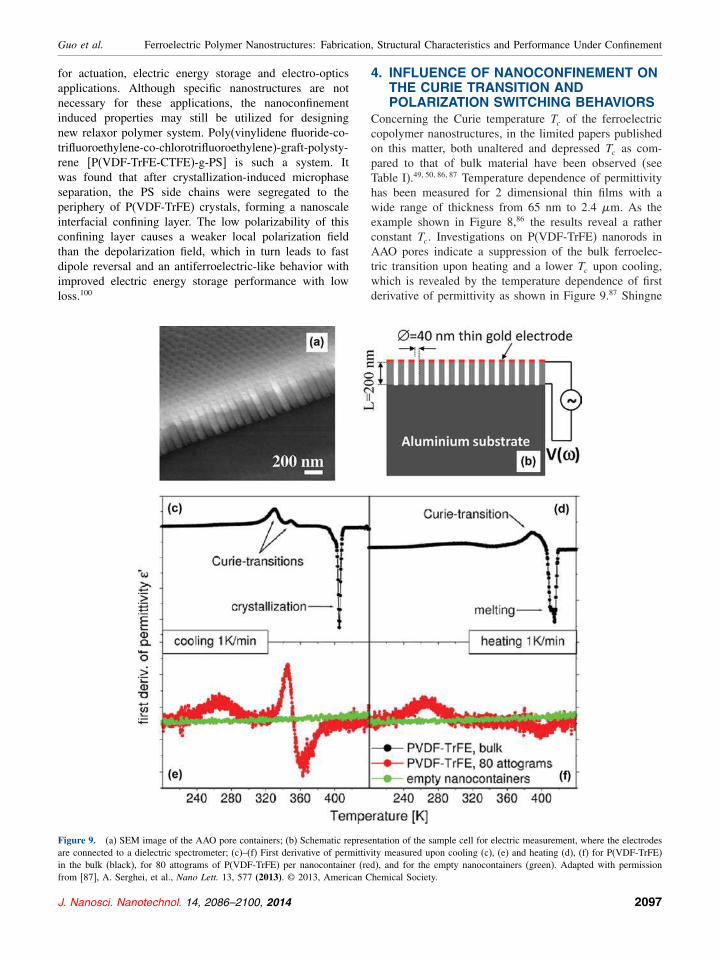
Figure 9. (a) SEM image of the AAO pore containers; (b) Schematic representation of the sample cell for electric measurement, where the electrodes
are connected to a dielectric spectrometer; (c)–(f) First derivative of permittivity measured upon cooling (c), (e) and heating (d), (f) for P(VDF-TrFE)
in the bulk (black), for 80 attograms of P(VDF-TrFE) per nanocontainer (red), and for the empty nanocontainers (green). Adapted with permission
from [87], A. Serghei, et al., Nano Lett. 13, 577 (2013). © 2013, American Chemical Society.
4. INFLUENCE OF NANOCONFINEMENT ONTHE CURIE TRANSITION ANDPOLARIZATION SWITCHING BEHAVIORS
Concerning the Curie temperature Tc of the ferroelectric
copolymer nanostructures, in the limited papers published
on this matter, both unaltered and depressed Tc as com-
pared to that of bulk material have been observed (see
Table I).49�50�86�87 Temperature dependence of permittivity
has been measured for 2 dimensional thin films with a
wide range of thickness from 65 nm to 2.4 �m. As the
example shown in Figure 8,86 the results reveal a rather
constant Tc. Investigations on P(VDF-TrFE) nanorods in
AAO pores indicate a suppression of the bulk ferroelec-
tric transition upon heating and a lower Tc upon cooling,
which is revealed by the temperature dependence of first
derivative of permittivity as shown in Figure 9.87 Shingne
J. Nanosci. Nanotechnol. 14, 2086–2100, 2014 2097

Ferroelectric Polymer Nanostructures: Fabrication, Structural Characteristics and Performance Under Confinement Guo et al.
Figure 10. (a) DSC heating and cooling scans for P(VDF-TrFE) bulk material and nanostructures with different diameters; (b) Melting temperature
(Tm) and Tc for various samples measured during heating after cooling with different scan rates; (c) Schematic of the Gibbs free energy for ferroelectric,
para electric and melt phase, where the increase in the Gibbs free energy due to confinement is shown by the dashed lines (Tm−b : melting temperature
of bulk, Tm−p: melting temperature in pores, Tc: Curie temperature); (d) free energy diagram of the ferroelectric, paraelectric and melt phases of
P(VDF-TrFE), where the dashed line shows the shift due to annealing in the paraelectric phase. Adapted with permission from [49], N. Shingne, et al.,
Polymer 54, 2737 (2013). © 2013, Elsevier B.V.
et al. carefully investigated the phase diagram of both
P(VDF-TrFE) bulk material and nanostructures of various
feature sizes fabricated by AAO template using differential
scanning calorimetry (DSC).49 As shown in Figure 10(a),
during cooling, the ferroelectric to paraelectric transition
temperature Tp−f covers a broad temperature range both
in the bulk and in the nanostructures. During heating,
the clear peak indicative of Tc remains basically unaf-
fected by nanoconfinement, although the Tm was changed.
This observation was explained by the similar influence
of nanoconfinement on the stability of ferroelectric and
the paraelectric phases as illustrated in Figure 10(b). Con-
cerning the annealing effect (Fig. 10(c)), with decreasing
cooling rate Tc decreases and Tm increases for bulk and
nanostructures with a feature size of 400 nm as a con-
sequence of the shifted free energy of the paraelectric
phase (Fig. 10(d)). For the nanostructure with a diameter
of 35 nm, however, the annealing effect is absent due to
the inhibited crystallization under confinement.
As for the transition character, both bulk type fer-
roelectric transition and different confining interface
induced second-order type ferroelectric transition was
observed.50 In addition, the polarization switching process
in copolymer nanomesa has also been studied by high
resolution PFM.101 A ‘Remote domain nucleation’ phe-
nomenon and spatially nonuniform wall velocity have been
observed, which were related to a random-bond type dis-
order associated with defects. This further reveals that
2098 J. Nanosci. Nanotechnol. 14, 2086–2100, 2014
Guo et al. Ferroelectric Polymer Nanostructures: Fabrication, Structural Characteristics and Performance Under Confinement
nanoconfinement may lead to switching behaviors that are
quite different from those of bulk ferroelectric polymers.
5. SUMMARYNanostructured ferroelectric polymer materials have
attracted intensive research interest in recent years due to
their great potential in a wide range of applications, par-
ticularly in new organic devices. In this article the tech-
niques that have been used for fabricating ferroelectric
polymer nanostructures over the last decade are briefly
reviewed. More importantly, the nanoconfinement induced
structural change, its influence on the physical proper-
ties of the ferrelectric polymer nanostructures as well as
the possible mechanisms are discussed. Among the tech-
niques, the ‘top-down’ NIL and the ‘bottom-up’ AAO
template synthesis are the two most promising ones that
are capable of generating ordered ferroelectric polymer
nanoscale patterns. However, challenges still remain on
how to achieve higher spatial resolution and better control
over microstructure (degree of order and desirable orien-
tation) and performance. Concerning the simple template
free self organization method, problems like poor control
over size and distribution and irregular morphology of the
nanostructures still need to be resolved. The limited exist-
ing publications indicate that nanoconfinement may induce
preferential molecular orientation, promote the formation
of polar ferroelectric phase, and these in turn may give rise
to improved but not deteriorated ferroelectricity or piezo-
electric response. The structure change may be attributed
to the modified inter-chain interactions or their interac-
tions with the confining surface. A deep understanding of
the detailed mechanisms underlying the microstructure and
performance evolution under nanoconfinement is a prereq-
uisite for future development of the relevant devices.
Acknowledgments: This work was supported by the
‘Hundred Talents Program’ of Chinese Academy of Sci-
ences, the National key Basic Research Program of China
(973 Program) under Grant No. 2013CB632900, and the
National Science Foundation of China under Grant No.
11074277.
References and Notes1. S. B. Lang and S. Muensit, Appl. Phys. A Mater. Sci. Process.
85, 125 (2006).
2. A. D. Handoko and G. K. L. Goh, Sci. Adv. Mat. 2, 16 (2010).
3. R. C. G. Naber, C. Tanase, P. W. M. Blom, G. H. Gelinck, A. W.
Marsman, F. J. Touwslager, S. Setayesh, and D. M. De Leeuw,
Nature Mater. 4, 243 (2005).
4. C. Chang, V. H. Tran, J. Wang, Y. K. Fuh, and L. Lin, Nano Lett.
10, 726 (2010).
5. S. Priya, J. Electroceram. 19, 167 (2007).
6. C. S. Jung, L. T. Lee, P. W. Jang, K. Seomoon, and K. H. Kim,
J. Nanosci. Nanotechnol. 12, 3326 (2012).
7. J. Zhang, A. A. Heitmann, S. P. Alpay, and G. A. Rossetti, Integr.
Ferroelectr. 125, 168 (2011).
8. C. S. Jung, L. T. Lee, P. W. Jang, K. Seomoon, and K. H. Kim,
J. Nanosci. Nanotechnol. 12, 3326 (2012).
9. P. F. Liu, J. L. Wang, X. J. Meng, J. Yang, B. Dkhil, and J. H. Chu,
New J. Phys. 12, 023035 (2010).
10. N. Setter and R. Waser, Acta Mater. 48, 151 (2000).
11. H. S. Nalwa, J. Macromol. Sci. Part C Polymer Reviews 31, 341
(1991).
12. Y. Takase, J. W. Lee, J. I. Scheinbeim, and B. A. Newman, Macro-
molecules 24, 6644 (1991).
13. J. Su, Z. Y. Ma, J. I. Scheinbeim, and B. A. Newman, J. Polym.
Sci. B 33, 85 (1995).
14. L. Yongjin, H. Shimizu, and T. Furumichi, J. Polym. Sci. B Polym.
Phys. 45, 2707 (2007).
15. S. Horiuchi and Y. Tokura, Nat. Mater. 7, 357 (2008).
16. A. J. Lovinger, Science 220, 4602 (1983).
17. H. S. Nalwa (ed.), Ferroelectric Polymers: Chemistry, Physics and
Applications, Marcel Dekker, New York (1995)
18. D. Guo, X. Chen, X. Chu, F. Zeng, Y. Bai, J. Cao, and B. Dkhil,
J. Appl. Phys. 113, 187210 (2013).
19. R. L. Jones, S. K. Kumar, D. L. Ho, R. M. Briber, and T. P. Russell,
Nature London 400, 146 (1999).
20. H. Kliem and R. Tadros-Morgane, J. Phys. D: Appl. Phys. 38, 1860
(2005).
21. D. Guo, I. Stolichnov, and N. Setter, J. Phys. Chem. B 115, 13455
(2011).
22. D. B. Li and D. A. Bonnell. Annu. Rev. Mater. Res. 38, 351 (2008).
23. Y. B.Yuan, T. J. Reece, P. Sharma, S. Poddar, S. Ducharme,
A. Gruverman, Y. Yang, and J. S. Huang, Nat. Mater.10, 296
(2011).
24. X. Qiu, J. Appl. Phys. 108, 011101 (2010).
25. J. Varghese, R. W. Whatmore, and J. D. Holmes, J. Mater. Chem. C
1, 2618 (2013).
26. M. Lazzari, C. Rodriguez-Abreu, and J. Rivas, J. Nanosci. Nan-
otechnol. 6, 892 (2006).
27. V. V. Kislyuk and O. P. Dimitriev, J. Nanosci. Nanotechnol. 8, 131
(2008).
28. N. Fukutake, N. Miyoshi, Y. Takasawa, T. Urakawa, T. Gowa,
K. Okamoto, A. Oshima, S. Tagawa, and M. Washio, Jpn. J. Appl.
Phys. 49, 065201 (2010).
29. H. M. Manohara, E. Morikawa, J. Choi, and P. T. Sprunger,
J. Microelectromech. S. 8, 417 (1999).
30. J. Choi, H. M. Manohara, E. Morikawa, P. T. Sprunger, P. A.
Dowben, and S. P. Palto, Appl. Phys. Lett. 76, 381 (2000).
31. Y. J. Kim, J. S. Hwan, and S. Y. Park, J. Nano. Sic. Nanotechnol.
11, 301 (2011).
32. C. C. Wu, S. L. C. Hsu, and I. L. Lo, J. Nanosci. Nanotech-
nol. 10, 6446 (2010).
33. S. W. Choi, J. Q. Han, J. Lim, and Jiseok, J. Nanosci. Nanotechnol.
11, 5921 (2011).
34. Z. J. Hu, G. Baralia, and V. Bayot, Nano Lett. 5, 1738, (2005).
35. S. J. Kang, Y. J. Park, J. Y. Hwang, H. Ju. Jeong, J. S. Lee, K. J.
Kim, H. C. Kim, J. Huh, and C. Park, Adv. Mater. 19, 581 (2007).
36. L. Zhang, S. Ducharme, and J. Y. Li, Appl. Phys. Lett. 91, 172906
(2007).
37. Z. J. Hu, M. W. Tian, B. Nysten, and A. M. Jonas, Nat. Mater.
8, 62 (2009).
38. Y. M. Liu, D. N. Weiss and J. Y. Li, ACS Nano 4, 83 (2010).
39. J. Martín, J. Maiz, J. Sacristan, and C. Mijangos, Polymer 53, 1149
(2012).
40. M. Steinhart, Adv. Polym. Sci. 123, 87 (2008).
41. H. Masuda and K. Fukuda, Science. 268, 1466 (1995).
42. M. Steinhart, S. Senz, R. B. Wehrspohn, U. Golsele, and J. H.
Wendorff, Macromolecules 36, 3646 (2003).
43. M. C. Garcıa-Gutierrez, A. Linares, J. J. Hernandez, D. R. Rueda,
T. A. Ezquerra, P. Poza, and R. J. Davies, Nano Lett. 10, 1472
(2010).
J. Nanosci. Nanotechnol. 14, 2086–2100, 2014 2099
Ferroelectric Polymer Nanostructures: Fabrication, Structural Characteristics and Performance Under Confinement Guo et al.
44. S. T. Lau, R. K. Zheng, H. L. W. Chan, and C. L. Choy, Mater.
Lett. 60, 2357 (2006).
45. X. Li, Y. F. Lim, K. Yao, F. E. H. Tay, and K. H. Seah, Phys. Chem.
Chem. Phys. 15, 515 (2013).
46. C. C. Wang, Q. D. Shen, S. C. Tang, Q. Wu, H. M. Bao, C. Z.
Yang, and X. Q. Jiang, Macromol. Rapid Commun. 29, 724 (2008).
47. B. Hilczer, E. Markiewicz, K. Pogorzelec-Glaser, M. Połomska,
and A. Pietraszko, Ferroelectrics 417, 124 (2011).
48. G. Canavese, S. Stassi, V. Cauda, A. Verna, P. Motto, A. Chiodoni,
S. L. Marasso, and D. Demarchi, IEEE Sens. J. 13, 2237
(2013).
49. N. Shingne, M. Geuss, B. Hartmann-Azanza, M. Steinhart, and
T. Thurn-Albrecht, Polymer 54, 2737 (2013).
50. J. L. Lutkenhaus, K. McEnnis, A. Serghei, and T. P. Russell, Macro-
molecules 43, 3844 (2010).
51. Y. J. Wu, Q. Z. Gu, G. Z. Ding, F. Q. Tong, Z. J. Hu, and A. M.
Jonas, ACS Macro. Lett. 2, 535 (2013).
52. J. H. Lin, S. G. Lu, M. Lin, M. Geu, and Q. M. Zhang, Appl. Phys.
Lett. 95, 022911 (2009).
53. S. Oh, Y. Kim, Y. Y. Choi, D. Kim, H. Choi, and K. No, Adv.
Mater. 24, 5708 (2012).
54. C. C. Hong, S. Y. Huang, J. Shieh, and S. H. Chen, Macromolecules
45, 1580 (2012).
55. V. Cauda, B. Torre, A. Falqui, G. Canavese, S. Stassi, T. Bein, and
M. Pizzi, Chem. Mater. 24, 4215 (2012).
56. P. R. Kumar, N. Khan, S. Vivekanandhan, N. Satyanarayana, and
A. K. Mohanty, J. Nanosci. Nanotechnol. 12, 1 (2012).
57. D. Mandal, S. Yoon, and K. J. Kim, Macromol. Rapid Commun.
32, 831 (2011).
58. S. Barik, H. H. Tan, J. W. Leung, and C. Jagadish, J. Nanosci.
Nanotechnol. 10, 1525 (2010).
59. R. Chapman, M. Danial, M. L. Koh, K. A. Jolliffe, and S. Perrier,
Chem. Soc. Rev. 41, 6023 (2012).
60. K. C. Barick and D. Bahadur, J. Nanosci. Nanotechnol. 10, 668
(2010).
61. C. Lu, H. Moehwald, and A. Fery, Soft Mater. 3, 1530 (2007).
62. S. Easwaramoorthi, P. Kim, and J. Lim, J. Mater. Chem. 20, 9684
(2010).
63. W. A. Zhang and A. H. E. Muller, Prog. Polym. Sci. 38, 1121
(2013).
64. J. Y. Li, Q. G. Du, and S. Ducharme, J. Appl. Phys. 104, 094302
(2008).
65. X. S. Chen, X. C. Chu, F. Zeng, J. Huang, and D. Guo, Sci. Adv.
Mater. 5, 1 (2013).
66. G. Reiter and G. R. Strobl, Progress in Understanding of Polymer
Crystallization, Springer, Berlin (2007).
67. D. Guo and N. Setter, Macromolecules 46, 1883 (2013).
68. H. Schmalz, A. Knoll, and A. J. Muller, Macromolecules 35, 10004
(2002).
69. T. Sakurai, H. Nagakura, S. Gondo, and S. Nojima, Polymer J.
45, 436 (2013).
70. J. Martın, C. Mijangos, A. Sanz, T. A. Ezquerra, and A. Nogales,
Macromolecules 42, 5395 (2009).
71. Q. Chen, K. Ren, B. Chu, Y. Liu, Q. M. Zhang, and V. A. Levstik,
Ferroelectrics 354, 178 (2007).
72. V. V. Kochervinskii, Crystallogr. Rep. 54, 1146 (2009).
73. H. Wu, Y. Cao, R. Ishige, Y. Higaki, T. Hoshino, N. Ohta, and
A. Takahara, Acs Macro. Letters 2, 414 (2013).
74. Y. Kikkawa, H. Abe, M. Fujita, T. Iwata, Y. Inoue, and Y. Doi,
Macromol. Chem. Phys. 204, 1822 (2003).
75. S. J. Kang, I. Bae, J. H. Choi, Y. J. Park, P. S. Jo, Y. K., K. J. Kim,
J. M. Myoung, E. Kim, and C. Park, J. Mater. Chem. 21, 3619
(2011).
76. B. Vanroy, M. Wubbenhorst, and S. Napolitano, ACS Macro. Lett.
2, 168 (2013).
77. S. Diaham, M. Bechara, M. L. Locatelli, and T. Lebey, J. Appl.
Phys. 110, 063703 (2011).
78. J. Maiz, J. Martin, and C. Mijangos, Langmuir 28, 12296 (2012).
79. F. X. Guan, J. Wang, J. L. Pan, Q. Wang, and L. Zhu, Macro-
molecules 43, 6739 (2010).
80. M. Mackey, D. E. Schuele, L. Zhu, L. Flandin, M. A. Wolak, J. S.
Shirk, A. Hiltner, and E. Baer, Macromolecules 45, 1954 (2012).
81. J. L. Keddle, R. A. L. Jones, and R. A. Cory, EuroPhys. Lett. 27, 59
(1994).
82. A. V. Bune, V. M. Fridkin, S. Ducharme, L. M. Blinov, S. P. Palto,
A. V. Sorokin, S. G. Yudin, and A. Zlatkin, Nature 391, 874 (1998).
83. R. C. G. Naber and P. W. M. Blom, J. Phys. D: Appl. Phys. 39, 503
(2006).
84. M. C. Garcia-Gutierrez, A. Linares, I. Martin-Fabiani, J. J.
Hernandez, M. Soccio, D. R. Rueda, T. A. Ezquerra, and
M. Reynolds, Nanoscale 5, 6006 (2013).
85. D. E. Martinez-Tong, M. Soccio, M. C. A. Nogales Garcia-
Gutierrez, D. R. Rueda, N. Alayo, F. Pérez-Murano, and T. A.
Ezquerra, Appl. Phys. Lett. 102, 191601 (2013).
86. K. Urayama, M. Tsuji, and D. Neher, Macromolecules 33, 8269
(2000).
87. A. Serghei, W. Zhao, D. Miranda, and T. P. Russell, Nano Lett. 13,
577 (2013).
88. J. B. Lando and W. W. Doll, Macromol. Sci., Part B: Phys. 2, 205
(1968).
89. E. Bellet-Amalric1 and J. F. Legrand, Eur. Phys. J. B 3, 225 (1998).
90. Y. Abe and K. Tashiro, Polymer 42, 3409 (2001).
91. M. Benz, W. B. Euler, and O. J. Gregory, Macromolecules 35, 2682
(2002).
92. W. Ma, J. Zhang, and X. J. Wang, Mater. Sci. 43, 398 (2008).
93. I. Martin-Fabiani, M. C. Garcia-Gutierrez, D. R. Rueda, A. Linares,
J. J. Hernandez, T. A. Ezquerra, and M. Reynolds, ACS. Appl.
Mater. Interfaces 5, 5324 (2013).
94. R. L. Jones, S. K. Kumar, D. L. Ho, R. M. Briber, and T. P. Russell,
Macromolecules 34, 559 (2001).
95. Y. Guan, G. M. Liu, P. Y. Gao, L. Li, G. Q. Ding, and D. J. Wang,
ACS Macro. Lett. 2, 181 (2013).
96. Q. M. Zhang, V. Bharti, and X. Zhao, Science 280, 2101 (1998).
97. D. Y. Jeong, Y. K. Wang, M. Huang, Q. M. Zhang, G. J. Kavarnos,
and F. Bauer, J. Appl. Phys. 96, 316 (2004).
98. X. Zhou, B. Chu, B. Neese, M. Lin, and Q. M. Zhang, IEEE Trans.
Dielectr. Electr. Insul. 14, 1133 (2007).
99. M. Valant, Prog. Mater. Sci. 57, 980 (2012).
100. F. X. Guan, J. Wang, L. Y. Yang, J. K. Tseng, K. Han, Q. Wang,
and L. Zhu, Macromolecules 44, 2190 (2011).
101. P. Sharma, J. R. Timothy, S. Ducharme, and G. Alexei, Nano Lett.
11, 1970 (2011).
Received: 12 October 2013. Accepted: 10 December 2013.
2100 J. Nanosci. Nanotechnol. 14, 2086–2100, 2014