field emission dark current of technical metallic ... · field emission dark current of technical...
TRANSCRIPT

arX
iv:p
hysi
cs/0
6100
90v3
[ph
ysic
s.ac
c-ph
] 1
0 Ja
n 20
07
SLS-TME-TA-2006-293 1
Field Emission Dark Current of
Technical Metallic Electrodes
F. Le Pimpec∗, R.Ganter, R. BetempsPaul Scherrer Institut
5232 VilligenSwitzerland
12 October 2006
Abstract
In the framework of the Low Emittance Gun (LEG) project, high gradient ac-celeration of a low emittance electron beam will be necessary. In order to achievethis acceleration, a -500 kV, 250 ns FWHM, pulse will be applied between two elec-trodes. Those electrodes should sustain the pulsed field without arcing, must notoutgas and must not emit electrons. Ion back bombardment, and dark current willbe damaging to the electron source as well as for the low emittance beam. Elec-trodes of commercially available OFE copper, aluminium, stainless steel, titaniumand molybdenum were tested, following different procedures including plasma glowdischarge cleaning.
\PACS 29.25.BX \sep 52.80.Vp \sep 79.70.+q
1 Introduction
In the framework of the Low Emittance Gun (LEG) project, an X-ray free-electron laser(FEL) based on a field emitting cathode is expected to deliver six orders of magnitudehigher peak brightness than current state-of-the-art light sources, together with a thou-sand times shorter pulses [1, 2].
To rapidly accelerate the electrons emitted by the electron source, and keep the emit-tance low, a stable pulsed voltage in the megavolt range is needed. The first project phaseis to design and test an ultra high vacuum (UHV) 500 kV pulser using a resonant air-coretransformer (Tesla coil) [3]. A pulse of 250 ns (full width at half maximum), -500 kV,working at 10Hz, will be applied between the cathode holder and an extracting anode.During this time, electrode materials should sustain the field without arcing and the darkcurrent should be kept as low as possible. This dark current will ionize the residual gas aswell as desorbing neutrals and ions by the known electron stimulated desorption process(ESD) [4, 5]. Those ions will be accelerated toward the cathode and the field emitter array
(FEA), in other words the electron source, and induce sputtering. It is known that somesurfaces are more sensitive than others to very low energy ion bombardment. Measurabledamage can already occur at 500 eV [6, 7, 8]. The damage induced, from any kind ofenergetic ions, will then reduce the electron emission and the lifetime of the field emitter,for example in GaAs photocathodes, used as polarized electron sources for accelerators[9, 10]. During the after pulse, the reversed field will accelerate the ions toward the ex-tracting anodes producing a current of electrons which will also back bombard the fieldemitter. The gas desorbed can induce a pressure rise which might not disappear beforethe next pulse. In the worst case, a plasma forms followed by breakdown and sputteringof the anode material to the field emitter cathode. Recent work, and thorough reviewof over a century of vacuum breakdown research in many areas, [11, 12, 13] is still notsufficient to select electrode materials without application specific testing.
In order to investigate the electrodes material, a DC high gradient test stand wasbuilt to test different metals, which were potentially suitable as electrodes in the pulser.The goal is to find the most suitable material, for our needs, which can sustain highfield without breakdown, and emits almost no electrons. In situ cleaning by plasma glowdischarge was also tested to see whether an improvement was noticeable in the mitigationof the dark current. This technique of gas conditioning to lower the field enhancementfactor β has already been reported [14, 15, 16] and used successfully in accelerators toprocess niobium accelerating cavities, see description in [12], as well as for curing otherissues [17].
2 System setup and electrode preparation
2.1 System setup
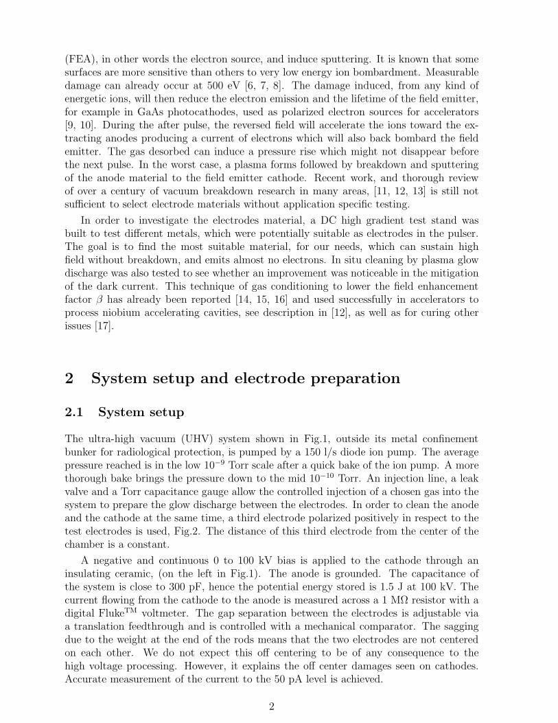
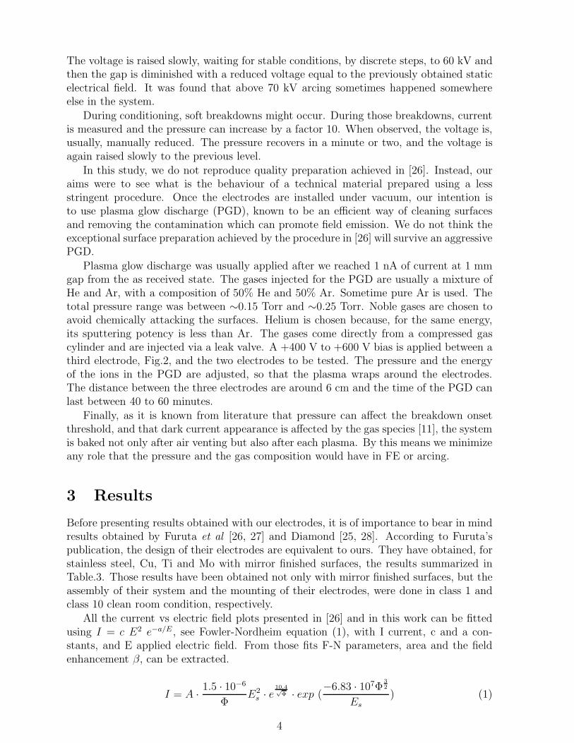
The ultra-high vacuum (UHV) system shown in Fig.1, outside its metal confinementbunker for radiological protection, is pumped by a 150 l/s diode ion pump. The averagepressure reached is in the low 10−9 Torr scale after a quick bake of the ion pump. A morethorough bake brings the pressure down to the mid 10−10 Torr. An injection line, a leakvalve and a Torr capacitance gauge allow the controlled injection of a chosen gas into thesystem to prepare the glow discharge between the electrodes. In order to clean the anodeand the cathode at the same time, a third electrode polarized positively in respect to thetest electrodes is used, Fig.2. The distance of this third electrode from the center of thechamber is a constant.
A negative and continuous 0 to 100 kV bias is applied to the cathode through aninsulating ceramic, (on the left in Fig.1). The anode is grounded. The capacitance ofthe system is close to 300 pF, hence the potential energy stored is 1.5 J at 100 kV. Thecurrent flowing from the cathode to the anode is measured across a 1 MΩ resistor with adigital FlukeTM voltmeter. The gap separation between the electrodes is adjustable viaa translation feedthrough and is controlled with a mechanical comparator. The saggingdue to the weight at the end of the rods means that the two electrodes are not centeredon each other. We do not expect this off centering to be of any consequence to thehigh voltage processing. However, it explains the off center damages seen on cathodes.Accurate measurement of the current to the 50 pA level is achieved.
2

2.2 Electrode choice
Given the long history of research on vacuum breakdown, it seems that the choice ofthe electrodes should be easy. However, as there is no universal quantifying theory toexplain the process of vacuum breakdown depending on the material, and its surface state(physical and chemical), it is necessary to do our own testing for our own application. Inorder to pick the most appropriate material, we study some elemental properties. Manytables of elements are then compiled in order to make an informed choice. In our case, theelectrodes should sustain a DC pulse of 500 kV and not produce or have a low electrondark current. Also a FEA will be installed in the middle of the cathode. If any arcingoccurs, sputtered, or vaporized, anode material will deposit on the FEA. This can lead todestruction of the FEA, and the necessity to exchange it; in our system this is a complexand time-consuming procedure. Table.1, compares the secondary electron yield (SEY)the sputtering rate, the melting point, and the tensile modulus of the candidate elements.
From Table.1, Cu and Au appear to be bad candidates. Results obtained with RFwaveguide support this point [22]. Despite its good electronic and ionic properties Alshould be discarded, as the combination of melting point and elastic modulus is lowcompared to other materials. Al will probably coat a FEA thoroughly in case of arcing,as we also found with a gold coated anode. The FEA coating problem further implies thatspark processing to reach high gradient, despite being efficient, should be avoided [23, 24],unless it is possible to protect the FEA. Some of the other materials which look good inthis table, can probably be discarded, due to their yield strength versus the temperatureor their electrical or thermal conductivity. Also the choice of the cathode and anodeshould be made separately as a good cathode material might not be so well suited as ananode. The respective choices depend on the geometry of the system, and the removal ofany heat generated by the dark current.
2.3 Electrode preparation and testing
All our electrodes tested have the same shape, see Fig.3 & 4 for the cathode and anode,respectively. The mean roughness was, by design, defined to be less than Ra ≤ 0.2µm.In Fig.4, the copper anode, has a hole in the middle. This hole was made to mimic thebehaviour of the extracting anode of the 500 kV pulser. None of the other electrodes havethis hole. The Ra of the electrodes was checked after high gradient testing.
The electrodes were cleaned using acetone and alcohol in an ultra-sonic bath, beforeinstallation in the UHV system. This is the ”as received” state. Unless specified otherwisenone of the surfaces have been mirror finished. All materials were commercially obtainedfrom GoodfellowTM. Technical materials refer to commercially available material, whichis exposed to air before installation.
Ti and Mo electrodes were fabricated by the same machining company. Electrodeswere thoroughly cleaned in acetone and alcohol before use. Ti electrodes were installedafter cleaning and tested, and Mo electrodes were vacuum fired at 900C for 3 h. AfterMo testing, Ti electrodes were also vacuum fired and reused. From the literature, it wasshown that heating up the material is beneficial in improving the breakdown strength[25].
The processing histories of the materials tested are summarized in Table.2. The pro-cedure of high gradient conditioning is the same for all the cathodes. The voltage betweenthe electrodes is applied for a given gap, 4 mm, 3 mm, 2 mm, 1.5 mm and then 1 mm.
3
The voltage is raised slowly, waiting for stable conditions, by discrete steps, to 60 kV andthen the gap is diminished with a reduced voltage equal to the previously obtained staticelectrical field. It was found that above 70 kV arcing sometimes happened somewhereelse in the system.
During conditioning, soft breakdowns might occur. During those breakdowns, currentis measured and the pressure can increase by a factor 10. When observed, the voltage is,usually, manually reduced. The pressure recovers in a minute or two, and the voltage isagain raised slowly to the previous level.
In this study, we do not reproduce quality preparation achieved in [26]. Instead, ouraims were to see what is the behaviour of a technical material prepared using a lessstringent procedure. Once the electrodes are installed under vacuum, our intention isto use plasma glow discharge (PGD), known to be an efficient way of cleaning surfacesand removing the contamination which can promote field emission. We do not think theexceptional surface preparation achieved by the procedure in [26] will survive an aggressivePGD.
Plasma glow discharge was usually applied after we reached 1 nA of current at 1 mmgap from the as received state. The gases injected for the PGD are usually a mixture ofHe and Ar, with a composition of 50% He and 50% Ar. Sometime pure Ar is used. Thetotal pressure range was between ∼0.15 Torr and ∼0.25 Torr. Noble gases are chosen toavoid chemically attacking the surfaces. Helium is chosen because, for the same energy,its sputtering potency is less than Ar. The gases come directly from a compressed gascylinder and are injected via a leak valve. A +400 V to +600 V bias is applied between athird electrode, Fig.2, and the two electrodes to be tested. The pressure and the energyof the ions in the PGD are adjusted, so that the plasma wraps around the electrodes.The distance between the three electrodes are around 6 cm and the time of the PGD canlast between 40 to 60 minutes.
Finally, as it is known from literature that pressure can affect the breakdown onsetthreshold, and that dark current appearance is affected by the gas species [11], the systemis baked not only after air venting but also after each plasma. By this means we minimizeany role that the pressure and the gas composition would have in FE or arcing.
3 Results
Before presenting results obtained with our electrodes, it is of importance to bear in mindresults obtained by Furuta et al [26, 27] and Diamond [25, 28]. According to Furuta’spublication, the design of their electrodes are equivalent to ours. They have obtained, forstainless steel, Cu, Ti and Mo with mirror finished surfaces, the results summarized inTable.3. Those results have been obtained not only with mirror finished surfaces, but theassembly of their system and the mounting of their electrodes, were done in class 1 andclass 10 clean room condition, respectively.
All the current vs electric field plots presented in [26] and in this work can be fittedusing I = c E2 e−a/E , see Fowler-Nordheim equation (1), with I current, c and a con-stants, and E applied electric field. From those fits F-N parameters, area and the fieldenhancement β, can be extracted.
I = A ·1.5 · 10−6
ΦE2
s · e10.4√
Φ · exp (−6.83 · 107Φ
3
2
Es) (1)
4

where Es = β ·E and the work function, for Mo, Φ is taken equal to 4.2 eV. However,we will not go further into the comparison between our measurements and theory, becausethe goal of this paper is to report on practical surface conditioning procedures to achievestable operation under a high electric field. It is also to report on the erosion of thematerials upon the field processing.
3.1 Aluminium Results
3.1.1 Al-Al electrodes
Pristine, as received Al electrodes were tested. The first test after a thorough bake of thechamber led to a dark current of 1nA at a gap of 1 mm for a field of 7.1 MV/m. The gapbetween the electrodes was set at 4 mm and the electrodes were conditioned overnight byapplying 29 kV and drawing 7 nA of current. The next day the dark current increased to13 nA. Several dark current curves were then produced and compared to the as receivedtest, Fig.5. The obvious conclusion is that our DC electrical conditioning did not lead toany improvement.
We next tested cleaning and conditioning using an He plasma of 0.26 Torr. Thesputtering rate of 500 eV He ions on Al is 0.16 [6]. The 1 nA at 1 mm gap was reached fora field of 13.5 MV/m. Subsequent He plasma continued to improve the results. However,a few breakdowns occurred during the voltage processing. An ArGD at a pressure of∼0.1 Torr produced the best results which are presented in Fig.6. The 1 nA at 1 mm gap(full circles) was reached for a field of 42 MV/m. When leaving the system at this level offield and dark current further improvement, decrease of dark current over time, is observedFig.6 full circles. In subsequent tests, also with different materials, this improvement wasoccasionally observed. However, in some cases the current increased to more than thedouble the previous value.
In the next test an He-Ar plasma was used to clean the same electrodes. The be-haviour, after pumping out the noble gases, was that no FE was observed until break-down. The Al electrodes held stably (12hours) a field of 42 MV/m without dark currentat 1.5 mm gap. Whilst the field was at 45 MV/m an arc occurred and an emissioncurrent of 350 nA could be measured. Nevertheless, damage due to this and furtherbreakdowns during the voltage processing, were not severe; the current at 1 mm, for afield of 41.5 MV/m was still only 1 nA. Finally, the best result obtained by He-Ar GD,was a field of 52 MV/m at 1 mm without dark current. However, at some point an arcmore violent than the previous ones, damaged the cathode so that no more GD was ableto restore the holding of the high electric field. A summary of the performance obtainedwith Al electrodes is shown in Table.4.
3.1.2 Mirror Finished Al Cathode
We then replaced the damaged Al cathode by a pristine mirror like finish Al (6082)cathode, machined to an Ra of 3 nm. The previously damaged mushroom anode wasreused, after wiping with alcohol before reinstallation in the UHV system. The damageon the anode was localized around the summit of the anode, and resembled the right-handpicture in Fig.7.
With this configuration, the as received system held stably without dark current, upto an electric field of less than 36 MV/m. At this value, an arc occurred. Inspection of
5

the cathode through the viewport of the UHV system showed pitting damage. An He-ArGD was then applied to cure and clean the electrodes. Results are summarized in Table.4.The column labelled <0.05 nA shows the field strength held without measuring any FE.The system held 90 MV/m electric field at 750 µm, and broke down at 92 MV/m. Thevacuum arcing was so severe that no further PGD was able to restore such fields. Finaldamage to the Al electrodes is shown in Fig.7. The high field sustained shows that thebreakdown is cathode initiated as the cathode was pristine and the anode was alreadyseverely damaged.
3.2 Copper results
Oxidized copper electrodes were tested solely after a PGD. Even after a PGD and thevoltage processing, the electrodes are still very oxidized. Cleaner spots around the holeof the anode were observed at the end of the testing. Damage on the cathode was alsovisible. The electrodes were then cleaned by chemical etching by use of a phosphoric
acid based solution Polynoxr. They were subsequently rinsed with tap water and afterdrying, cleaned with ethanol. A last test was conducted by installing a mirror diamondturned OFHC Cu cathode (Ra ∼ 3 nm) and the already used Mo and then a SS anode.
3.2.1 Cu-Cu electrodes
The results obtained seem to show that there is no influence from the anode hole in theachievement of the high gradient, as our results are similar to what was obtained in [26],see Table.3 for clean copper.
In comparison to Al electrodes, craters in the Cu were neither as deep, nor as extended: see the 2 spots in Fig.3, compared to damages in Fig.7. All breakdown damage onthe Cu anode remained localized around the hole of the mushroom. That suggests twopossibilities without excluding a combination of the two. The energy in the arc was notsufficient to vaporize the Cu materials, by melting and sputtering the melted Cu, despitethe fact that Cu has a higher sputtering rate than Al. Or the field was not strong enoughto pull out droplets of Cu which could have then been vaporized [29].
3.2.2 Mirror finished Cu cathode
As results from Al seemed to indicate that the breakdown is cathode initiated, a com-bination of a mirror finished cathode with the previously used Mo (vacuum fired ) andstainless steel(SS) anodes was tested. Those anodes had sustained damaged far less sig-nificant than the Al anode pictured in Fig.7. Results of the Cu-Mo conditioning areshown in Table.5. The conditioning of the ”as received” electrode followed the ”break-down processing” or spark processing scheme, until a more severe breakdown brought theCu cathode to emit at the level of 800 nA, at 3 mm gap. During the first 500 eV ArGD,small breakdowns could be seen on the Cu cathode, which were probably dust burningaway. Results obtained after plasma processing improved the situation but not to thelevel of the two clean Cu electrodes. It was expected that higher fields could be reached,as in the case of using two Cu electrodes, Table.5, or two Mo electrodes (see Table.6).
The Mo anode was exchanged for a SS anode, and the Cu cathode was turned 180
on its axis. Because the anode arm sags, damage on the cathode is not localized on thecenter of the anode, hence allowing a pristine area to be exposed. The maximum field
6
held with this pair was 11 MV/m at 3 mm gap, after an ArGD. From these last results,no conclusion should be drawn on the coupling of this last pair as the Cu cathode wasalready exhibiting an oxide color. The presence of the oxide can be due to oxygen presentin the ArGD, or from oxygen being released from the Mo anode during high voltageconditioning see §3.3.5. The copper oxide is present from the center of the Cu sample to5 mm from the sample circular edge. Microscopy and surface analysis did not reveal anymaterial transfer from the anode (Mo or SS) to the Cu cathode.
3.3 Stainless steel, titanium and molybdenum results
Main results obtained, at 1 mm, for stainless steel (SS), Ti and Mo are summarized inTable.6.
3.3.1 Stainless Steel
SS electrodes were electrically processed the same way as Al electrodes. After plasmatreatment, the best field achieved was 68 MV/m with dark current below the 10 pAdetection limit. The final breakdown, was not recoverable by the use of a PGD. Uponremoval of the electrodes, damage was located at the top of the mushroom. However,craters were not as deep or as wide as for Al electrodes (in Fig.7). The damage is lessextended than that observed on the Cu electrodes. If we look at the data in Table.1, thisis not surprising. Effectively, both the melting point and the Young’s modulus of SS arefar above copper values. However, as tiny amounts of vaporized or sputtered materialfrom the anode can be prejudicial to the working of FEAs, avoiding even soft breakdownsseems to be a good strategy.
3.3.2 Titanium
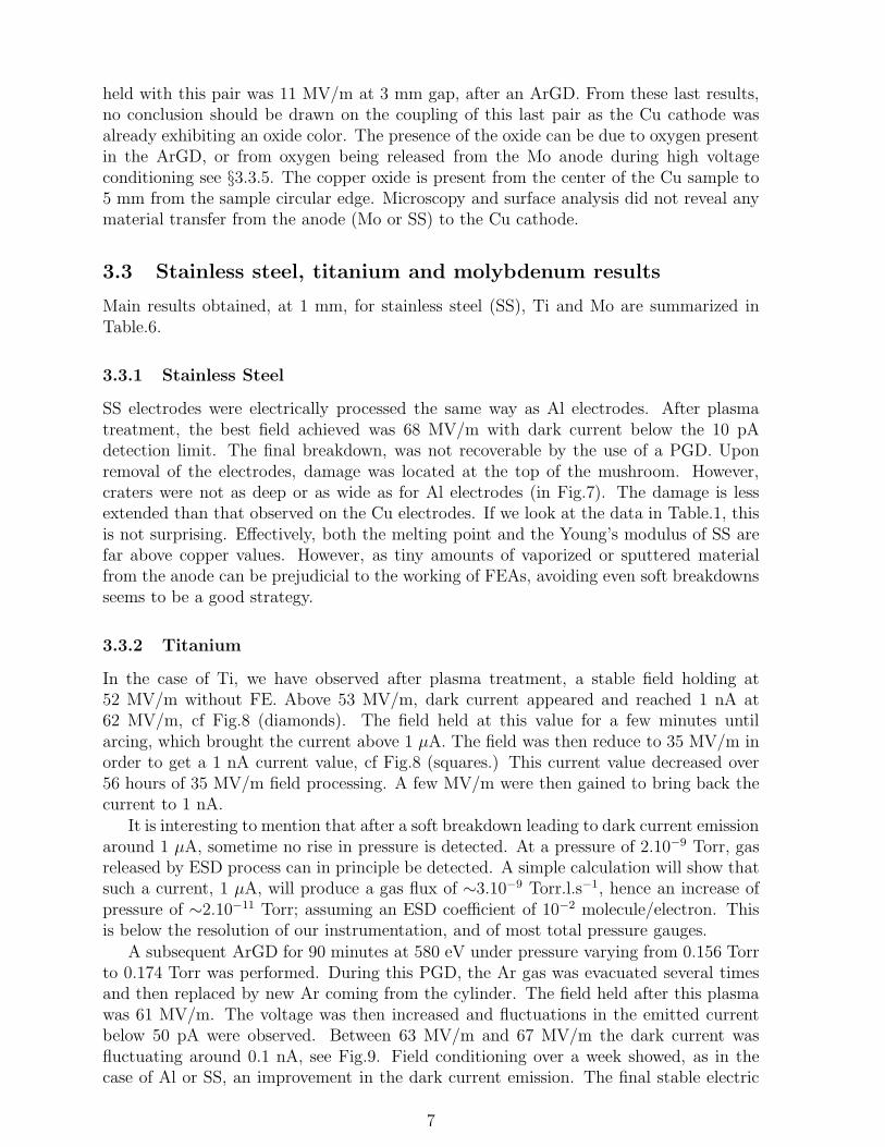
In the case of Ti, we have observed after plasma treatment, a stable field holding at52 MV/m without FE. Above 53 MV/m, dark current appeared and reached 1 nA at62 MV/m, cf Fig.8 (diamonds). The field held at this value for a few minutes untilarcing, which brought the current above 1 µA. The field was then reduce to 35 MV/m inorder to get a 1 nA current value, cf Fig.8 (squares.) This current value decreased over56 hours of 35 MV/m field processing. A few MV/m were then gained to bring back thecurrent to 1 nA.
It is interesting to mention that after a soft breakdown leading to dark current emissionaround 1 µA, sometime no rise in pressure is detected. At a pressure of 2.10−9 Torr, gasreleased by ESD process can in principle be detected. A simple calculation will show thatsuch a current, 1 µA, will produce a gas flux of ∼3.10−9 Torr.l.s−1, hence an increase ofpressure of ∼2.10−11 Torr; assuming an ESD coefficient of 10−2 molecule/electron. Thisis below the resolution of our instrumentation, and of most total pressure gauges.
A subsequent ArGD for 90 minutes at 580 eV under pressure varying from 0.156 Torrto 0.174 Torr was performed. During this PGD, the Ar gas was evacuated several timesand then replaced by new Ar coming from the cylinder. The field held after this plasmawas 61 MV/m. The voltage was then increased and fluctuations in the emitted currentbelow 50 pA were observed. Between 63 MV/m and 67 MV/m the dark current wasfluctuating around 0.1 nA, see Fig.9. Field conditioning over a week showed, as in thecase of Al or SS, an improvement in the dark current emission. The final stable electric
7

field obtained for 1 nA at 1 mm gap is 55 MV/m, see insert in Fig.9. Above this level offield, the dark current does not diminish but it increases with time, Fig.9.
Upon inspection of the electrodes after their extraction from the chamber, damagespots can be seen on both electrodes. Damage is located on the anode around the topof the mushroom, and 4 separate spots can be seen on the cathode spread over a trail of1 cm length. Damage on the Ti anode is similar to that seen on the SS and Cu anodes,in extension and morphology (melted area).
3.3.3 Molybdenum
Vacuum fired Mo electrodes were installed in the system, the best results are summarizedin Table.6. A simple 25Hz optical camera was used to view the electrodes, hence the spacein between. When running, no light is present in the system enclosure. During the softevents, a flash is seen on the TV screen and a jump in current intensity, below 0.1 nA, ismeasured sometimes associated with a pressure increase. The flash is localized and takesthe full space occupied between the electrodes. During harder breakdowns, sound can beheard coming from the enclosure. After these soft breakdowns, the voltage could still beincreased. In order to have a chance to detect breakdown precursor, fast acquisition andvery high sensitivity, to single photon, are mandatory. However, such a simple opticalsystem can be used as an interlock protection for our FEL.
As for the Ti electrodes, dark current appears at some voltage, contrary to Al, Cu andSS electrodes where dark current appears only after a breakdown. Raising the field furtherincreased the dark current until breakdown occurred. Dark current plots from as receivedelectrodes(triangles), and after three plasma treatments are presented in Fig.10. The firstArGD pushed the limits of the dark current onset (diamonds) until a hard breakdownoccurred, bringing the current into the µA range. The onset and the 1 nA limit wasthen greatly reduced (squares). The second ArGD enabled partial recuperation fromthis breakdown (asterisks). A third plasma He-Ar, did not bring any extra improvement(crosses in squares). Mo conditioning from broad electrodes at large gap (> 500µm) wassimilar to conditioning with short gaps. Mo reached a higher gradient than Cu but itsparked more to get there [24], hence showing more damage than Cu, Fig.3. From this,it is obvious that a special electrode conditioning procedure must be used to process theMo electrodes, and thus to protect the electron source (FEA).
3.3.4 Titanium vacuum fired
Original Ti electrodes were re-installed after vacuum firing and the results, for comparisonwith non fired Ti, are presented in Table.6. After vacuum firing the Ti became gray black.This color can indicate TiH2 or TiO2 in the rutile form, or Ti3O5. Damage, all localizedon the top of Ti anode, can be seen in Fig.4. The involuntary coating is removed by thesevere breakdowns sustained by both electrodes.
3.3.5 Surface analysis
Given the rather poor performances in field holding for the Mo electrodes, comparedto literature values, and the colour of the Ti electrodes, it is suspected that the vacuumfiring degraded the Mo properties instead of improving them. The pressure in the vacuumfurnace was probably around 10−5 Torr. Ti and Mo cathodes were sent for surface analysis,X-ray photoelectron (XPS) and Auger (AES) spectroscopy. Upon AES analysis, the
8

surfaces of both electrodes exhibited high contents of carbon (C) and oxygen (O), higherthan normal air exposure. Nitrogen (N) is also present on the Mo surface. Nitrogencannot be seen on Ti as Ti and N overlap under AES analysis. Under XPS analysis, ashift of about 5 eV to higher binding energy, for both Mo 3d5/2 and Ti 2p3/2 is observed.Such shift can be the mark of TiO2 and MoO3 [30]. The Mo shows no discoloration,suggesting the formation of a thin trioxide film. The conclusions are, first of all a smallair leak might have been present in the furnace. Secondly, a bad heat treatment will bringthe opposite results in terms of field holding.
4 Conclusions
Plasma glow discharge is a very effective way to enhance the DC field holding in betweentwo broad electrodes. It also permits restoration and sometimes improvement of the DCfield limit achieved after a breakdown event leading to dark current emission. This darkcurrent follows the FN law.
The downside of such treatment, for Al, Cu and SS electrodes, is that the surfaces holdthe field until breakdown with no or little warning. No increase in pressure is recorded, butsometime some current variation in the tens of pA might appear. Such fluctuations canbe the sign of a forthcoming breakdown, if any, but the time scale can vary from minutesto hours. In the hunt for the breakdown precursor, in the framework of an interlock forthe 500 kV pulser, a highly sensitive and fast photomultiplier will be tested in this 100 kVDC test stand.
For Ti and Mo electrodes dark current appears and increases when raising the voltageuntil breakdown occurs. However, during the processing a few sparks occur, sometimesin a ”spitfest” regime. Those sparks are beneficial as they condition the surface. Darkcurrent at a level of 1 nA can either drift to hundreds of nA, fall back to less than ahundred pA or stay stable. So far, the prediction for its evolution is only empirical.
Finally we have, without stringent procedures, matched or exceeded results obtainedby other labs. However, results for non mirror finished Ti and Mo were below the onesobtained elsewhere. In the case of Mo, it is suspected that the vacuum firing contaminatedthe Mo as it did for Ti, leading to poorer performances than usually reported in theliterature.
In order to find the Grail material, which will hold our requested field without emittingdark current, Niobium seems to be a material of interest. Ion implantation, with nitrogen,is known to harden materials [31, 32]. It may be possible that this technique of hardeningcan be useful to increase the breakdown threshold of soft materials, as it seems to havefor harder ones [33]. Dark current from electrodes can be lowered by depositing a puremonolayer of oxygen on the surface, which will increase the work function of the electrodes.However, and in the framework of an accelerator electron source, this layer might haveto be regenerated frequently as back bombardement from residual gas ions will clean thesurface.
5 Acknowledgments
Kugler GMBH for the donation of the mirror finished Al and Cu cathodes. R. Kirby(SLAC) and U. Mueller (EMPA Duebendorf) for the surface analysis. S. Ritter (PSI) for
9

the SEM time. Finally, to M. Taborelli, T. Ramsvik, S. Sgobba at CERN and E. Kirk(PSI) for some useful discussion.
References
[1] R. Bakker. LEG Project Overview. In First annual EUROFEL workshop, Or-say/Saclay, France, 2005.
[2] A.E Candel. Simulation of Electron Source for Next-Generation X-ray Free-ElectronLaser. PhD thesis, Ecole Polytechnique Federale Zurich, 2005. ETHZ-IPP 2005-11.
[3] M. Paraliev, C. Gough, S. Ivkovic. Tesla coil design for electron gun application . In15th IEEE International Pulsed Power Conference, Monterey, USA, 2005.
[4] P.A Redhead. The First 50 Years of Electron Stimulated Desorption (1918-1968).Vacuum, 48 (6):585, 1997.
[5] R.D. Ramsier and J.T. Yates Jr. Electron-Stimulated Desorption: Principles andApplications. Surface Science Reports, 12 (6-8):243, 1991.
[6] J.L. Vossen, W. Kern. Thin Film processes. Academic Press, 1978.
[7] S. Cernusca. Electron Emission and Nanodefects due to Slow Ion Impact on SolidSurfaces. PhD thesis, Technischen Universitat Wien, 2003.
[8] I.C. Gebeshuber, S. Cernusca, F. Aumayr, HP. Winter. AFM search for slow MCI-produced nanodefects on atomically clean monocrystalline insulator surfaces. NuclearInstruments and Methods in Physics Research B, 205:751, 2003.
[9] R. Dei-Cas. Review of High - brightness Electron Guns. In EPAC, Berlin, Germany,1992.
[10] J. Grames et al. Lifetime Measurements using the JLAB load-lock Gun. In PESP,Mainz, Germany, 2004.
[11] L.L Laurent. High Gradient RF Breakdown Studies. PhD thesis, University of Cali-fornia Davis, 2002.
[12] G.R. Werner. Probing and Modeling Voltage Breakdown in Vacuum. PhD thesis,Cornell University, 2004.
[13] D.M. Goebel. High Voltage Breakdown Limits of Molybdenum and Carbon-basedGrids for Ion Thrusters. In 41st AIAA/ASME/SAE/ASEE Joint Propulsion Con-ference & Exhibit, 2005. AIAA 2005-4257.
[14] R.J. Noer. Electron Field Emission from Broad-Area Electrodes. Applied Physics A,28:1–24, 1982.
[15] S. Kobayashi, H. Kojima, Y. Saito. Influence of in-situ ion beam sputter cleaning onthe conditioning effect of vacuum gaps. In SPIE - Discharges and Electrical Insulationin Vacuum, volume 2259, page 364, 1994.
10

[16] S. Kobayashi. Recent Experiments on Vacuum Breakdown of Oxygen-Free CopperElectrodes. IEEE Trans. DEI, 4:841, 1997.
[17] R. Calder, A. Grillot, F. Le Normand and A.G Mathewson. Cleaning and SurfaceAnalysis of Stainless Steel Ultrahigh Vacuum Chambers by Argon Glow Discharge.In Proc. of the 7th Int. Vac. Congress, 1977. IVC & ICSS Vienna, Austria.
[18] David R. Lide, editor. Handbook of Chemistry and Physics. 74th edition.CRC PRESS, 1994.
[19] W.M. Posadowski, Z.J. Radzimski. Sustained self-sputtering using a direct currentmagnetron source. Journal of Vacuum Science and Technology, A11(6), 1993.
[20] A. Anders et al. Self-Sustained Self-Sputterinng: A Possible Mechanism for theSuperdense Glow Phase of a Peudopark. IEEE Transactions on Plasma Science, 23(3):275, 1995.
[21] R.S. Mason and M. Pichilingi. Sputtering in a glow discharge ion source - pressuredependence: theory and experiment. J. Phys. D :Appl Phys, 27:2363, 1994.
[22] V. Dolgashev and S.G. Tantawi. RF breakdown in X-band Waveguides. In EPAC2002, France, 2002. SLAC-PUB-10355.
[23] D.W. Williams and W.T. Williams. Effect of electrode surface finish on electricalbreakdown in vacuum. J. Phys.D:Appl.Phys, 5:1845, 1972.
[24] M. Kildemo, S. Calatroni, M. Taborelli. Breakdown and Field Emission Conditioningof Cu, Mo and W. Phys. Rev. Special Topics - Accelerators and Beams, 7, 2004.
[25] W.T Diamond. New perspectives in vacuum high voltage insulation. I. The transitionto field emission. Journal of Vacuum Science and Technology, A16(2), 1998.
[26] F. Furuta et al. Reduction of Field Emission Dark Current for High-Field Gradi-ent Electron Gun by Using a Molybdenum Cathode and Titanium Anode. NuclearInstruments and Methods in Physics Research A, 538:33–44, 2005.
[27] C. Suzuki et al. Fabrication of ultra-clean copper surface to minimize field emissiondark currents. Nuclear Instruments and Methods in Physics Research A, 462:337,2001.
[28] W.T Diamond. New perspectives in vacuum high voltage insulation. II. Gas desorp-tion. Journal of Vacuum Science and Technology, A16(2), 1998.
[29] G.A. Mesyats and S.A. Barengolts. The ”Hunting Effect” in the cathode region of avacuum arc. In ICPIG 2003, Germany, 2003.
[30] Handbook of X-Ray Photoelectron Spectroscopy. Perkin-Elmer Corporation, 1992.
[31] E. Woolley. Hardness goes skin-deep. Materials World,, 5(10):515, 1997.http://www.azom.com/details.asp?ArticleID=552.
[32] A. Shokouhy et al. Surface modification of AISI 304 Stainless Steel using nitrogenion implantation. In ICPIG 2005, Holland, 2005.
11

[33] C.K. Sinclair et al. Dramatic Reduction of DC Field Emission from Large AreaElectrodes by Plasma-Source Ion Implantation. In PAC,Chicago, USA, 2001.
12

Table 1: Secondary electron yield maximum [18], sputtering yield by 500 eV incident Ar[6] and self-sputtering rate at 500 eV of different elements [19, 20].
Elements SEYmax Atm/Ar inc Self Sputter Melting Point Young Modulusrate TC GPa
Cu 1.3 2.3 > 1 1083 110Al 1.0 1.05 < 1 660 69Au 1.4 2.4 > 1 1063 78Ti 0.9 0.5 < 1 1668 116Mo 1.25 0.6 < 1 2610 329Zr 1.1 0.65 < 1 1852 68Fe 1.3 1 (SS 1.3) ∼ 1 [21] 1536 200W 1.4 0.57 < 1 3410 411Ta 1.3 0.57 < 1 2996 186Nb 1.2 0.6 < 1 2415 105
Table 2: Measurement history of air-exposed dark current electrodes.
Cathode AnodeAs Plasma
nth Plasmareceived (He - Ar)
SS SS Yes Yes YesAl Al Yes Yes Yes
Al mirror Finished Al (sme as abv) Yes Yes YesCu oxidized Cu oxidized - Yes Yes
Cu PolynoxTM Cu PolynoxTM Yes Yes -Ti Ti Yes Yes Yes
Mo vac fired Mo vac fired Yes Solely Ar YesTi vac fired Ti vac fired Yes Solely Ar Yes
Cu mirror Finished Mo vac fired Yes Solely Ar Yes
13

Table 3: Field gradient (MV/m) between electrodes obtained at 1 mm gap for 1 nA ofdark current or with no field emission (FE), second row.
SUS Cu Ti Mo Mo - Ti Al Nb1 nA [26] 36 47.5 88 84 103 - -
No FE [25] - 70 60 - - 85 92
Table 4: Electric field in MV/m held in between two Al electrodes at 1 mm gap for thegiven dark current in nA.
Al - Al Al mirror finished - AlState / Dark Current < 0.05 nA 1 nA < 0.05 nA 1 nA
As Received - 7.5 36 (2 mm) 29After Plasma 52 30 73 (stable) 31
(92 at 750µm)
Table 5: Electric field in MV/m held in between Cu electrodes at 1 mm gap for the givendark current in nA. (*) obtained at 3mm gap
Cu oxidized Cu clean Cu-MoState / Dark Current < 0.05 nA 1 nA < 0.05 nA 1 nA < 0.05 nA 1 nA
As Received - - 24 26 18.2 (*) 13.8 (*)After Plasma 32 29.3 55 19 21.6 25.4
Table 6: Electric field in MV/m held in between two SS two Ti and two Mo electrodes at1 mm gap for the given dark current in nA.
State / Dark Current < 0.05 nA 1 nA
SSAs Received 40 42.5After Plasma 68 35
TiAs Received 50 46.6After Plasma 63 67 (0.1nA)
Ti As Received 29.6 32.5
Vac Fired After Plasma 39 41.4
Mo As Received 37 45.2
Vac Fired After Plasma 44 61.3
14

Figure 1: Dark Current -100 kV DC test stand.
15

Figure 2: Dark Current -100 kV DC test stand. Zoom over the area containing thecathode (flat electrode) the anode (mushroom) and the plasma electrode located at 7 cmfrom the center of the system
16

Figure 3: Cleaned Cu cathode after high voltage testing, left. Damaged Mo cathode,right picture. Damage can be clearly seen.
Figure 4: Three anodes used for HV testing, Ti on the left(grey black colour, after vacuumfiring), Mo in the center and Cu on the right. Pictures taken after HV testing. Damagecan be seen on the Ti electrodes
17

0.0
0.5
1.0
1.5
2.0
2.5
3.0
3.5
4.0
4.5
2.5 3.5 4.5 5.5 6.5 7.5 8.5 9.5E (MV/m)
I (n
A)
4000 microns 3000 microns
2000 microns 1500 microns
1000 microns 700 microns
500 microns
Figure 5: Dark current of Al electrodes after a system bake at 190C for 100h and afterelectrical conditioning of 29 kV at a 4 mm gap drawing 7 nA of current from the cathodeto the anode.
0.0
0.2
0.4
0.6
0.8
1.0
1.2
1.4
1.6
20 25 30 35 40 45 50 55 60E (MV/m)
I (n
A)
500 microns
1000 microns
1500 microns
2000 microns
3000 micronsOvernight
Improvement
Figure 6: Dark current of Al electrodes after an Ar Glow Discharge, following the previousHe processing and high field conditioning.
18

Figure 7: Breakdown damage withstood by the Al cathode (mirror finished-left) andanode (right) during the conditioning period. Scale in cm.
0.0
0.2
0.4
0.6
0.8
1.0
1.2
1.4
35 36 37 38 39 40 41 42 43 44 45 46 47 48 49 50 51 52 53 54 55 56 57 58 59 60 61 62E (MV/m)
I (n
A)
1000 microns
1000 microns aftr 2nd brkdn
Dark current <0.05nA
Hold 52 MV/m (1 mm)
P~1.9 10-9
Torr
Curring over 56h
Degradation over time
few minutes
Fluctuation
Current
increase
Figure 8: Dark current evolution of Ti electrodes after a 2nd Ar Glow Discharge. Thesquare curve is obtained after a surface breakdown at 62 MV/m
19

0.0
0.2
0.4
0.6
0.8
1.0
1.2
1.4
36 38 40 42 44 46 48 50 52 54 56 58 60 62 64 66 68E (MV/m)
I (n
A)
1000 microns
P~1.9 10-9
Torr
Curring over
a week
Current increase to 400
nA reduce E to 38MV/m
00.5
11.5
22.5
33.5
4
54.8 55.0 55.2 55.4 55.6 55.8
Da
rkc
Cu
rre
nt
(nA
) 1000 micronsfluctuations
Degradation
over 1 hour
Improvement
over 30 min
Degradation
over 12 hours
Figure 9: Dark current evolution of Ti electrodes after a 3rd Ar Glow Discharge.
Mo electrodes, 1 mm GAP
0.0
0.2
0.4
0.6
0.8
1.0
1.2
1.4
1.6
20 22 24 26 28 30 32 34 36 38 40 42 44 46 48 50 52 54 56 58 60 62 64E (MV/m)
I (n
A)
As received1st plasma1st plasma, after Hard BRKD2nd Plasma3rd plasma
Degradation
over 72h
Hard
Breakdown
improvement
over 20 min
Curing
over 72h
Drifted to 17nA
after 72 hours
Few
minutes
Drifted to 38 nA,
reduced Voltage
Figure 10: Dark current evolution of Mo electrodes after processing.
20

List of Tables
1 Secondary electron yield maximum [18], sputtering yield by 500 eV incidentAr [6] and self-sputtering rate at 500 eV of different elements [19, 20]. . . . 13
2 Measurement history of air-exposed dark current electrodes. . . . . . . . . 133 Field gradient (MV/m) between electrodes obtained at 1 mm gap for 1 nA
of dark current or with no field emission (FE), second row. . . . . . . . . . 144 Electric field in MV/m held in between two Al electrodes at 1 mm gap for
the given dark current in nA. . . . . . . . . . . . . . . . . . . . . . . . . . 145 Electric field in MV/m held in between Cu electrodes at 1 mm gap for the
given dark current in nA. (*) obtained at 3mm gap . . . . . . . . . . . . . 146 Electric field in MV/m held in between two SS two Ti and two Mo elec-
trodes at 1 mm gap for the given dark current in nA. . . . . . . . . . . . . 14
21

List of Figures
1 Dark Current -100 kV DC test stand. . . . . . . . . . . . . . . . . . . . . . 152 Dark Current -100 kV DC test stand. Zoom over the area containing the
cathode (flat electrode) the anode (mushroom) and the plasma electrodelocated at 7 cm from the center of the system . . . . . . . . . . . . . . . . 16
3 Cleaned Cu cathode after high voltage testing, left. Damaged Mo cathode,right picture. Damage can be clearly seen. . . . . . . . . . . . . . . . . . . 17
4 Three anodes used for HV testing, Ti on the left(grey black colour, aftervacuum firing), Mo in the center and Cu on the right. Pictures taken afterHV testing. Damage can be seen on the Ti electrodes . . . . . . . . . . . . 17
5 Dark current of Al electrodes after a system bake at 190C for 100h andafter electrical conditioning of 29 kV at a 4 mm gap drawing 7 nA of currentfrom the cathode to the anode. . . . . . . . . . . . . . . . . . . . . . . . . 18
6 Dark current of Al electrodes after an Ar Glow Discharge, following theprevious He processing and high field conditioning. . . . . . . . . . . . . . 18
7 Breakdown damage withstood by the Al cathode (mirror finished-left) andanode (right) during the conditioning period. Scale in cm. . . . . . . . . . 19
8 Dark current evolution of Ti electrodes after a 2nd Ar Glow Discharge. Thesquare curve is obtained after a surface breakdown at 62 MV/m . . . . . . 19
9 Dark current evolution of Ti electrodes after a 3rd Ar Glow Discharge. . . . 2010 Dark current evolution of Mo electrodes after processing. . . . . . . . . . . 20
22