film capacitors - ec.kemet.com€¦ · resistance low high dv/dt high restriction self-healing no...
TRANSCRIPT

© 2019 KEMET Corporation
Film Capacitors
Design and Characteristics

© 2019 KEMET Corporation
Design
© 2019 KEMET Corporation
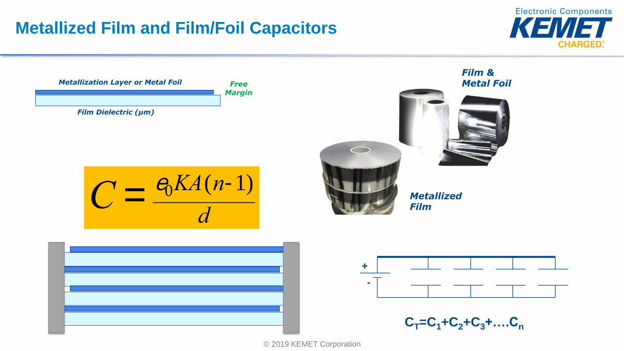
Metallization Layer or Metal Foil Free Margin
Film Dielectric (µm)
C = e0KA(n-1)
d
+
-
CT=C1+C2+C3+….Cn
Film &Metal Foil
MetallizedFilm
Metallized Film and Film/Foil Capacitors

© 2019 KEMET Corporation
Characteristics
© 2019 KEMET Corporation
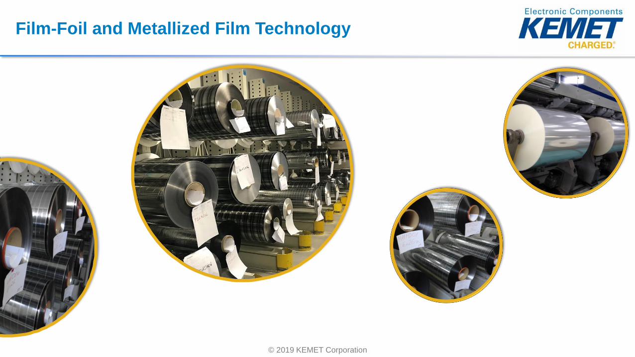
Film-Foil and Metallized Film Technology
© 2019 KEMET Corporation
Film-Foil and Metallized Film Technology
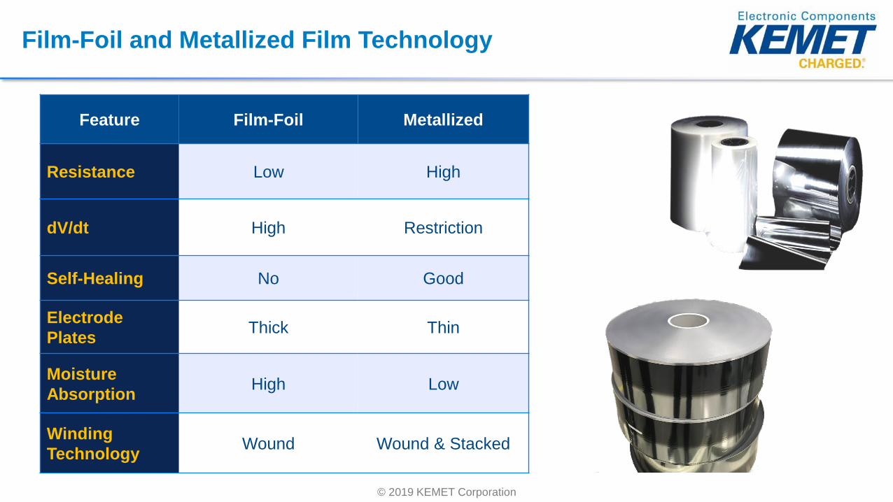
Feature Film-Foil Metallized
Resistance Low High
dV/dt High Restriction
Self-Healing No Good
Electrode
PlatesThick Thin
Moisture
AbsorptionHigh Low
Winding
TechnologyWound Wound & Stacked
© 2019 KEMET Corporation
Film-Foil and Metallized Film Technology
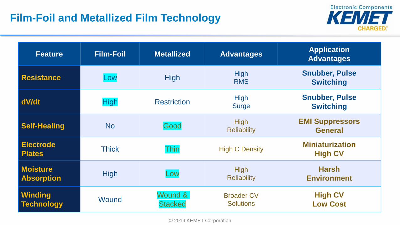
Feature Film-Foil Metallized AdvantagesApplication
Advantages
Resistance Low HighHigh
RMS
Snubber, Pulse
Switching
dV/dt High RestrictionHigh
Surge
Snubber, Pulse
Switching
Self-Healing No GoodHigh
Reliability
EMI Suppressors
General
Electrode
PlatesThick Thin High C Density
Miniaturization
High CV
Moisture
AbsorptionHigh Low
High
Reliability
Harsh
Environment
Winding
TechnologyWound
Wound &
Stacked
Broader CV
Solutions
High CV
Low Cost

© 2019 KEMET Corporation
Winding Constructions I
Single Design
Single Layer
Film Foil
Dual Section
Single Layer
(Series)
Single Design
Multi-Layer
•Standard•General Purposes•Self-Healing
•High Current•No Self-Healing
•Higher Voltage•Self-Healing
•High Breakdown Voltage•Self-Healing
© 2019 KEMET Corporation
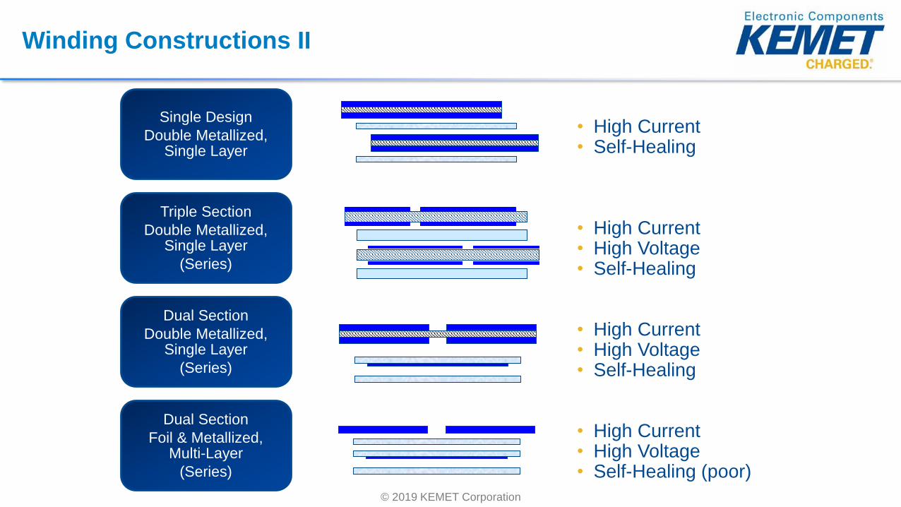
Single Design
Double Metallized, Single Layer
Triple Section
Double Metallized, Single Layer
(Series)
Dual Section
Double Metallized, Single Layer
(Series)
Dual Section
Foil & Metallized, Multi-Layer
(Series)
• High Current• Self-Healing
• High Current• High Voltage• Self-Healing
• High Current• High Voltage• Self-Healing
• High Current• High Voltage• Self-Healing (poor)
Winding Constructions II
© 2019 KEMET Corporation
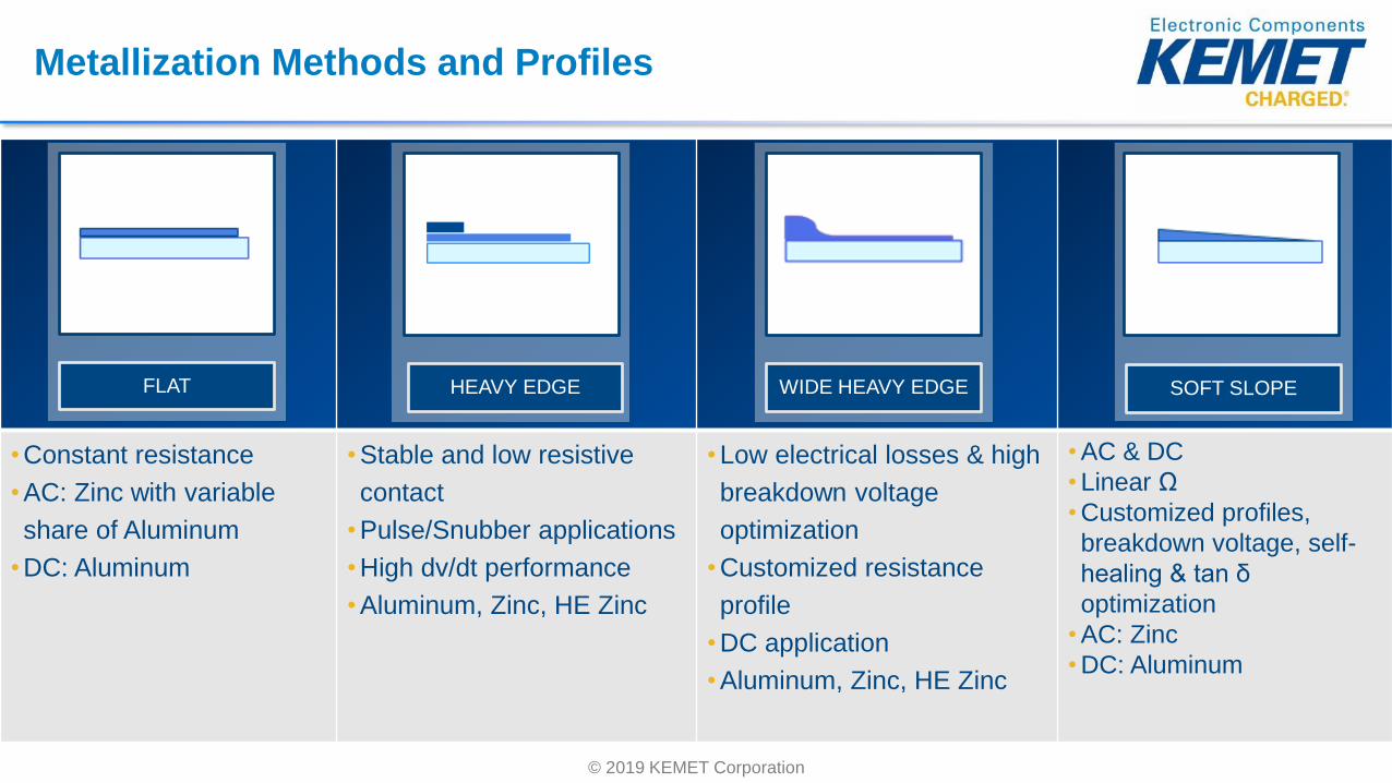
• Constant resistance
• AC: Zinc with variable
share of Aluminum
• DC: Aluminum
• Stable and low resistive
contact
• Pulse/Snubber applications
• High dv/dt performance
• Aluminum, Zinc, HE Zinc
• Low electrical losses & high
breakdown voltage
optimization
• Customized resistance
profile
• DC application
• Aluminum, Zinc, HE Zinc
• AC & DC
• Linear Ω
• Customized profiles,
breakdown voltage, self-
healing & tan δ
optimization
• AC: Zinc
• DC: Aluminum
Metallization Methods and Profiles
FLAT HEAVY EDGE WIDE HEAVY EDGE SOFT SLOPE

© 2019 KEMET Corporation
Wound and Stacked Technology

© 2019 KEMET Corporation
• Great performances for peak voltage
withstanding
• Can be used with all film dielectrics
• Can use the lowest film thickness
• 1.0 µm PET; 2.4 µm PP
• Max. Voltage: 2,000 Vdc
• Cost effectiveness
• High number of capacitors produced per a
single frame
• Used mostly on small radial and SMD
• High capacitance volume efficiency
• High intrinsic peak current withstanding (dV/dt)
• Limited maximum voltage vs. wound
Wound and Stacked Technology
© 2019 KEMET Corporation
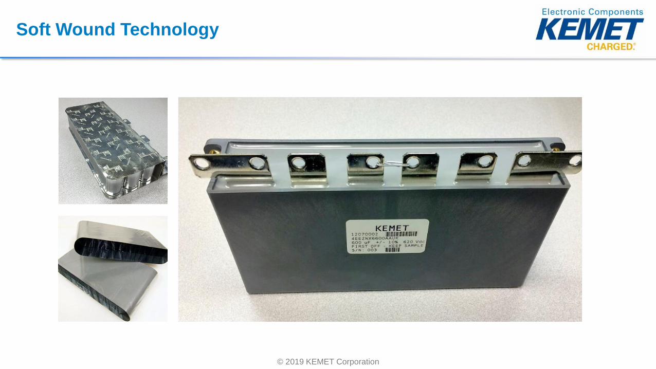
Soft Wound Technology
© 2019 KEMET Corporation
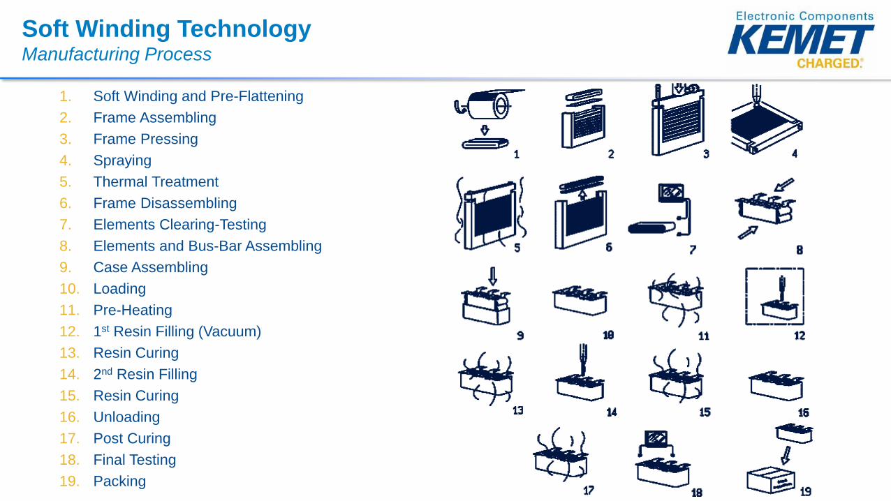
Soft Winding TechnologyManufacturing Process
1. Soft Winding and Pre-Flattening
2. Frame Assembling
3. Frame Pressing
4. Spraying
5. Thermal Treatment
6. Frame Disassembling
7. Elements Clearing-Testing
8. Elements and Bus-Bar Assembling
9. Case Assembling
10. Loading
11. Pre-Heating
12. 1st Resin Filling (Vacuum)
13. Resin Curing
14. 2nd Resin Filling
15. Resin Curing
16. Unloading
17. Post Curing
18. Final Testing
19. Packing

© 2019 KEMET Corporation
Winding
© 2019 KEMET Corporation
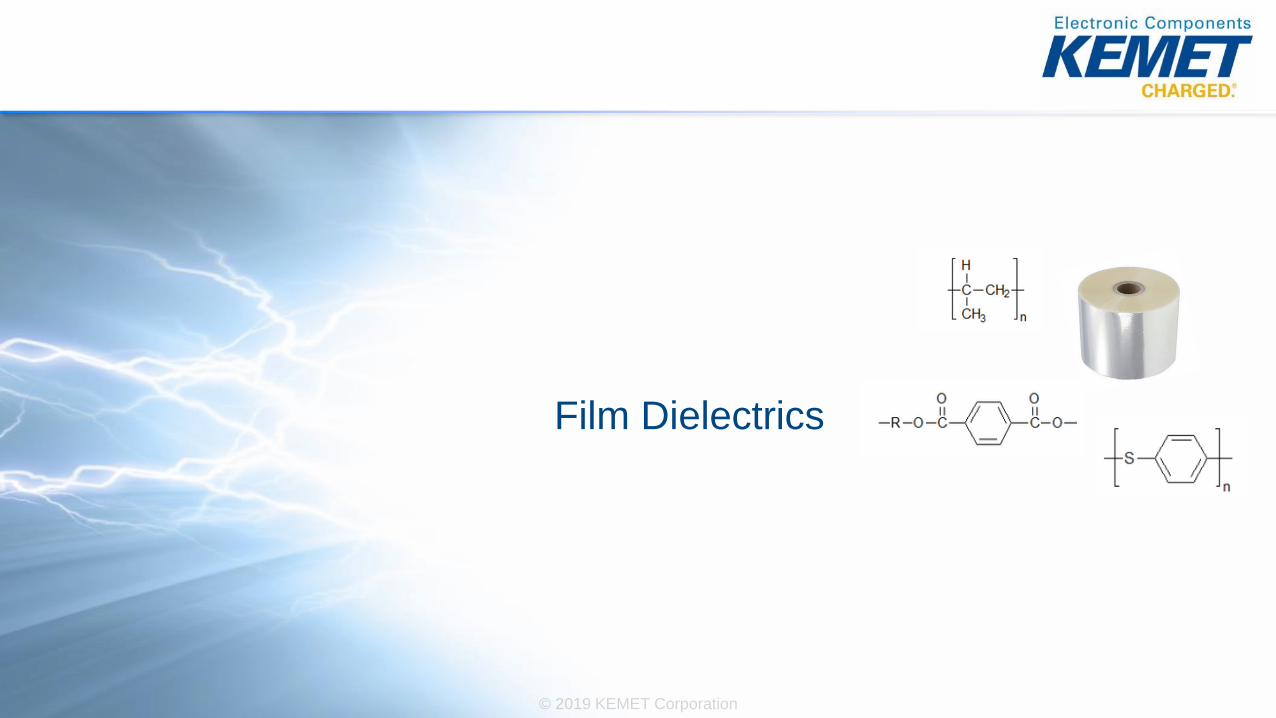
Film Dielectrics

© 2019 KEMET Corporation
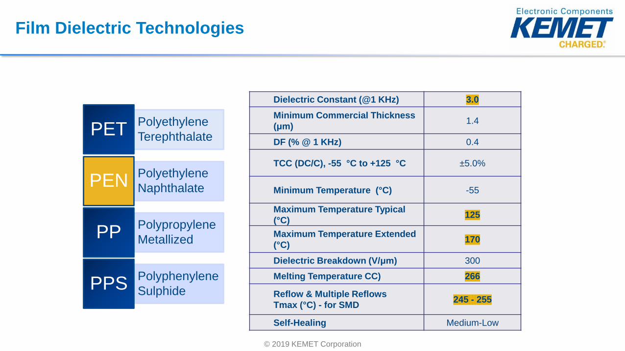
Film Dielectric Technologies
Polyethylene
TerephthalatePET
Polyethylene
NaphthalatePEN
Polypropylene
MetallizedPP
Polyphenylene
SulphidePPS
Dielectric Constant (@1 KHz) 3.3
Minimum Commercial Thickness
(μm) 0.9
DF (% @ 1 KHz) 0.5
TCC (DC/C), -55 °C to +125 °C ±5.0%
Minimum Temperature (°C) -55
Maximum Temperature Typical
(°C)125
Maximum Temperature Extended
(°C) 150
Dielectric Breakdown (V/μm) 280
Melting Temperature CC) 254
Reflow & Multiple Reflows
Tmax (°C) - for SMD245
Self-Healing Medium
© 2019 KEMET Corporation
Dielectric Constant (@1 KHz) 3.0
Minimum Commercial Thickness
(μm) 1.4
DF (% @ 1 KHz) 0.4
TCC (DC/C), -55 °C to +125 °C ±5.0%
Minimum Temperature (°C) -55
Maximum Temperature Typical
(°C)125
Maximum Temperature Extended
(°C) 170
Dielectric Breakdown (V/μm) 300
Melting Temperature CC) 266
Reflow & Multiple Reflows
Tmax (°C) - for SMD245 - 255
Self-Healing Medium-Low
Film Dielectric Technologies
Polyethylene
TerephthalatePET
Polyethylene
NaphthalatePEN
Polypropylene
MetallizedPP
Polyphenylene
SulphidePPS

© 2019 KEMET Corporation
Dielectric Constant (@1 KHz) 2.2
Minimum Commercial Thickness
(μm) 2.2 1.9
DF (% @ 1 KHz) 0.02
TCC (DC/C), -55 °C to +125 °C ±2.5%
Minimum Temperature (°C) -55
Maximum Temperature Typical
(°C)105
Maximum Temperature Extended
(°C) 125
Dielectric Breakdown (V/μm) 400
Melting Temperature CC) 178
Reflow & Multiple Reflows
Tmax (°C) - for SMDNO
Self-Healing Excellent
Film Dielectric Technologies
Polyethylene
TerephthalatePET
Polyethylene
NaphthalatePEN
Polypropylene
MetallizedPP
Polyphenylene
SulphidePPS

© 2019 KEMET Corporation
Dielectric Constant (@1 KHz) 3.0
Minimum Commercial Thickness
(μm) 1.2
DF (% @ 1 KHz) 0.05
TCC (DC/C), -55 °C to +125 °C ±5.0%
Minimum Temperature (°C) -55
Maximum Temperature Typical
(°C)125
Maximum Temperature Extended
(°C) 170
Dielectric Breakdown (V/μm) 220
Melting Temperature CC) 283
Reflow & Multiple Reflows
Tmax (°C) - for SMD260
Self-Healing Low
Film Dielectric Technologies
Polyethylene
TerephthalatePET
Polyethylene
NaphthalatePEN
Polypropylene
MetallizedPP
Polyphenylene
SulphidePPS

© 2019 KEMET Corporation
Film Dielectric Technologies
Polyethylene
TerephthalatePET
Polyethylene
NaphthalatePEN
Polypropylene
MetallizedPP
Polyphenylene
SulphidePPS
-60 -10 40 90
-4
-3
-2
-1
0
1
2
3
4
Tamb (°C)
ΔC
/C (
%)
PET PP PPS PEN
𝑓 = 1𝑘𝐻𝑧
-3
-2.5
-2
-1.5
-1
-0.5
0
0.5
1
0.1 1 10 100
ΔC
/C (
%)
f(kHz)
PP PPS PEN PET
© 2019 KEMET Corporation
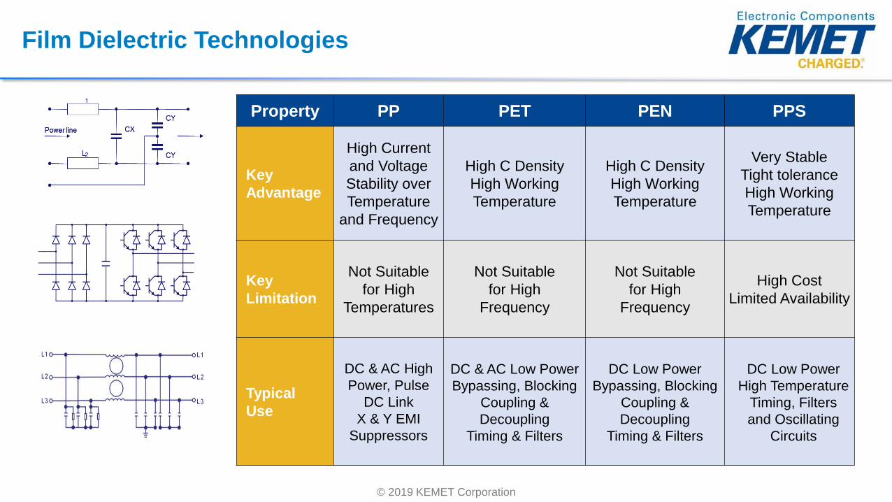
Film Dielectric Technologies
Property PP PET PEN PPS
Key
Advantage
High Current
and Voltage
Stability over
Temperature
and Frequency
High C Density
High Working
Temperature
High C Density
High Working
Temperature
Very Stable
Tight tolerance
High Working
Temperature
Key
Limitation
Not Suitable
for High
Temperatures
Not Suitable
for High
Frequency
Not Suitable
for High
Frequency
High Cost
Limited Availability
Typical
Use
DC & AC High
Power, Pulse
DC Link
X & Y EMI
Suppressors
DC & AC Low Power
Bypassing, Blocking
Coupling &
Decoupling
Timing & Filters
DC Low Power
Bypassing, Blocking
Coupling &
Decoupling
Timing & Filters
DC Low Power
High Temperature
Timing, Filters
and Oscillating
Circuits
© 2019 KEMET Corporation
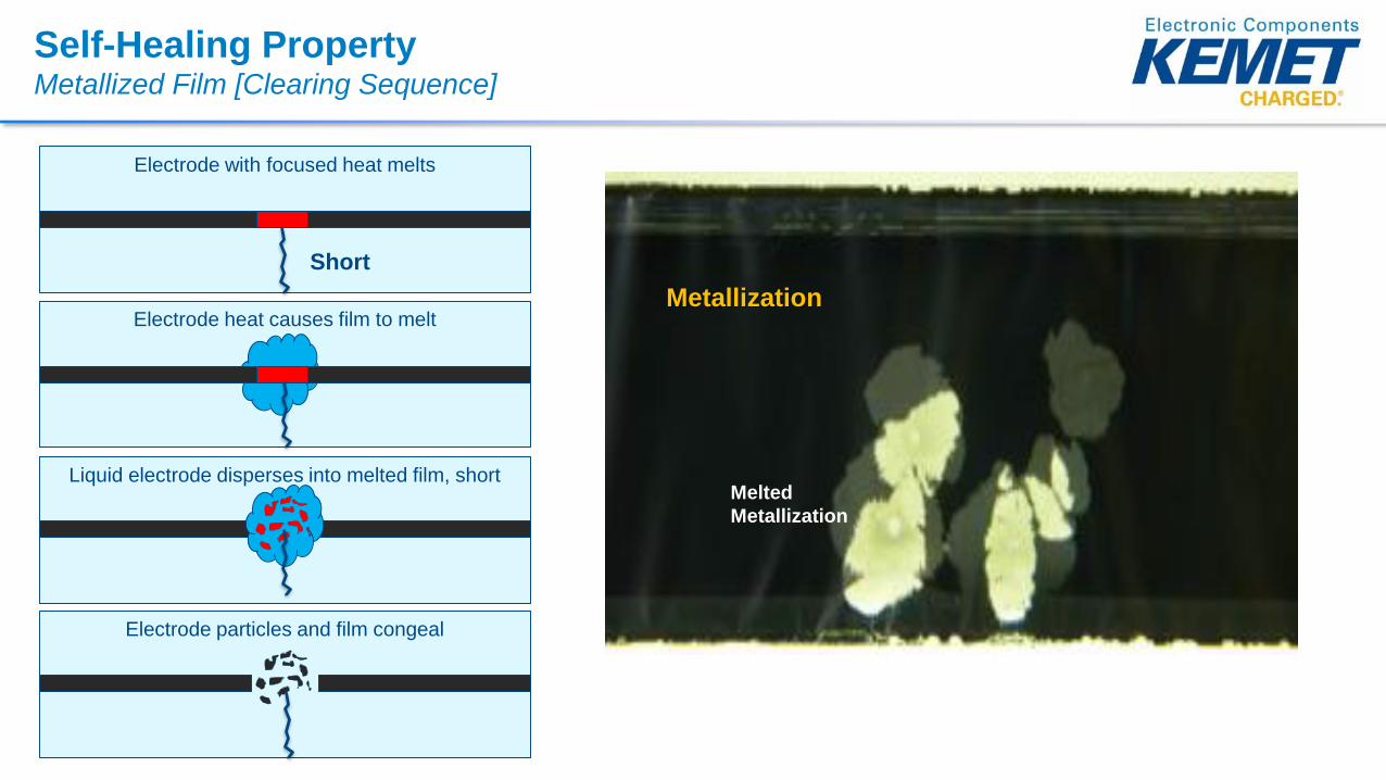
Self-Healing Property Metallized Film [Clearing Sequence]
Electrode with focused heat melts
Electrode heat causes film to melt
Liquid electrode disperses into melted film, short
opens
Electrode particles and film congeal
Short
Melted
Metallization
Metallization
© 2019 KEMET Corporation
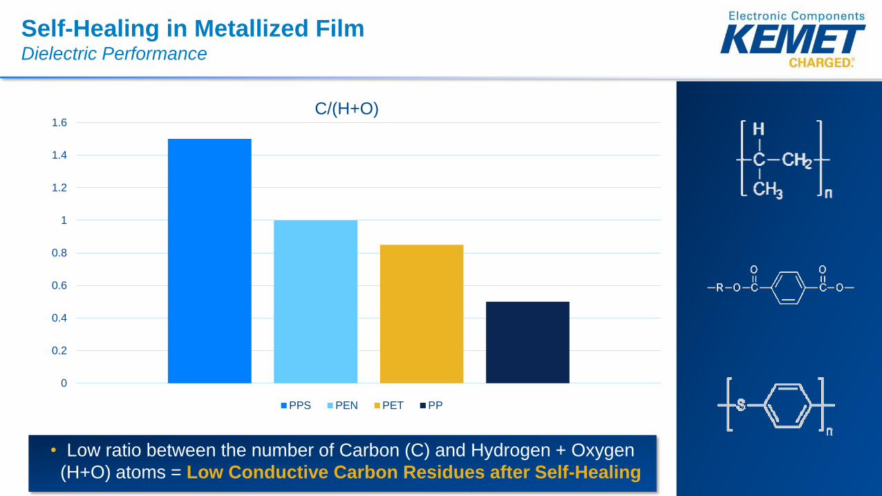
Self-Healing in Metallized Film Dielectric Performance
• Low ratio between the number of Carbon (C) and Hydrogen + Oxygen
(H+O) atoms = Low Conductive Carbon Residues after Self-Healing
0
0.2
0.4
0.6
0.8
1
1.2
1.4
1.6C/(H+O)
PPS PEN PET PP
© 2019 KEMET Corporation
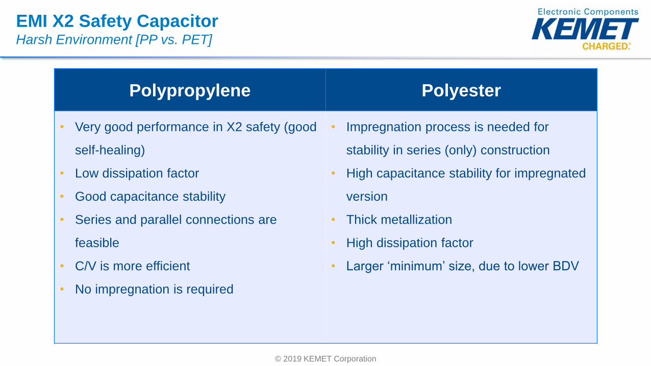
EMI X2 Safety Capacitor Harsh Environment [PP vs. PET]
Polypropylene Polyester
• Very good performance in X2 safety (good
self-healing)
• Low dissipation factor
• Good capacitance stability
• Series and parallel connections are
feasible
• C/V is more efficient
• No impregnation is required
• Impregnation process is needed for
stability in series (only) construction
• High capacitance stability for impregnated
version
• Thick metallization
• High dissipation factor
• Larger ‘minimum’ size, due to lower BDV

© 2019 KEMET Corporation
Film Capacitor Market Demand TrendLong Life with High Stability & Reliability
IEC 60384-14 Am.1 Ed.4Fixed capacitors for use in Electronic Equipment
I.2 Humidity
Robustness Grades
Test Damp Heat,
Steady State at Rated
Voltage
Grade Test Condition A Test Condition B
I 40 °C / 93 % RH 21 days 85 °C / 85 % RH 168 h
II 40 °C / 93 % RH 56 days 85 °C / 85 % RH 500 h
III 60 °C / 93 % RH 56 days 85 °C / 85 % RH 1,000 h
Measurement Requirement
Capacitance |ΔC| ≤10 %
Dissipation Factor0,024 for CN ≤ 1 μF
0,015 for CN > 1 μF
Insulation Resistance >50 % of the applicable limits
© 2019 KEMET Corporation
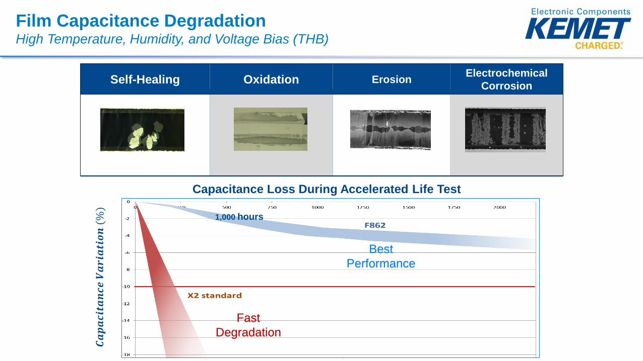
Self-Healing Oxidation ErosionElectrochemical
Corrosion
Film Capacitance Degradation High Temperature, Humidity, and Voltage Bias (THB)
Capacitance Loss During Accelerated Life Test
𝑪𝒂𝒑𝒂𝒄𝒊𝒕𝒂𝒏𝒄𝒆𝑽𝒂𝒓𝒊𝒂𝒕𝒊𝒐𝒏(%
)
1,000 hours
Best
Performance
Fast
Degradation

© 2019 KEMET Corporation
Capacitance Decreasing MechanismsSelf-Healing & Corona (with Transient)
Key Parameters Self-Healing
• Polyproplylene dielectric (best)
• Metallization profile, material and thickness
• Exclusion of air and humidity during
manufacturing
Lost
Metal
Metal

© 2019 KEMET Corporation
Capacitance Decreasing MechanismsOxidation
Zn° ⇌ Zn2+ + 2 e- 2 Zn°+ O2 ⇌ ZnO
• Process active with or without presence of applied AC voltage
• Capacitance decrease is due to the metal oxidation
• Capacitors encapsulation in plastic box reduces significantly the
magnitude of this phenomenon
© 2019 KEMET Corporation
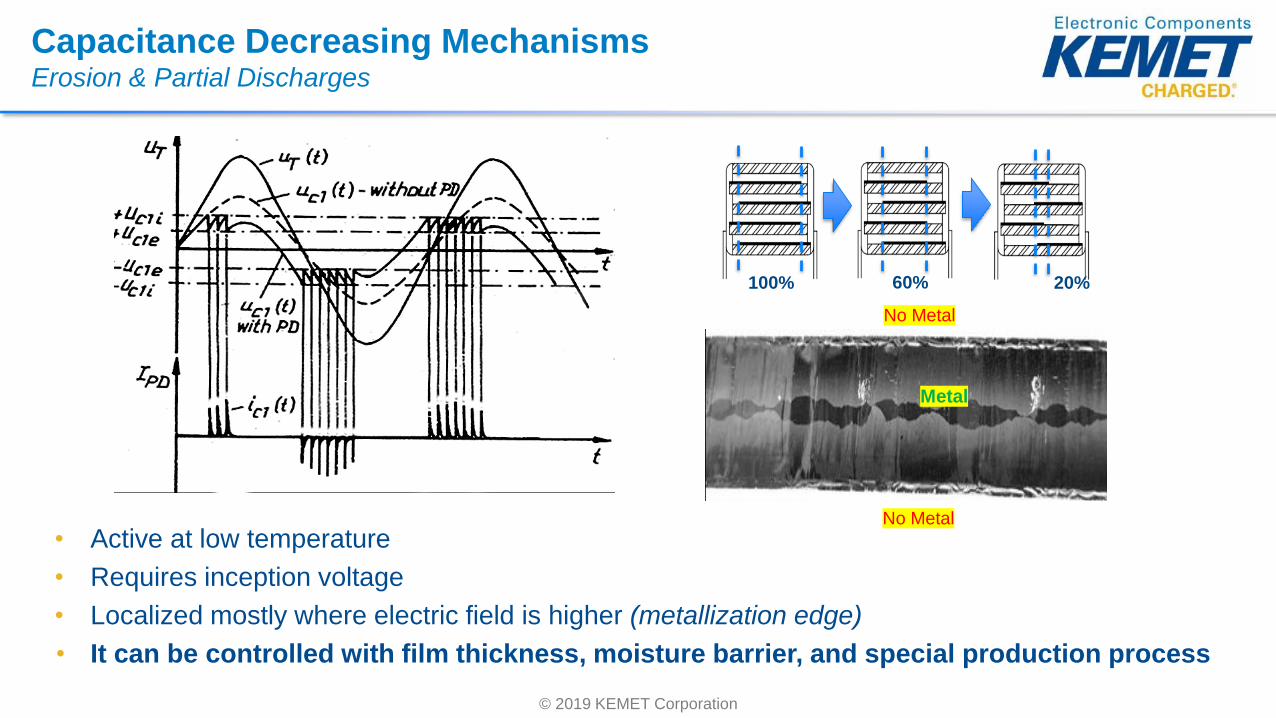
Capacitance Decreasing MechanismsErosion & Partial Discharges
• Active at low temperature
• Requires inception voltage
• Localized mostly where electric field is higher (metallization edge)
• It can be controlled with film thickness, moisture barrier, and special production process
No Metal
Metal
100% 60% 20%
No Metal

© 2019 KEMET Corporation
Capacitance Decreasing MechanismsElectrochemical Corrosion
Electrochemical Cell
Applied
AC Voltage
Air Gap
Induced
VoltageZn° → Zn2+ + 2 e-
2 H2O + 2 e- → H2 + 2 OH-
No Metal
Metal
• Reactions in the electrochemical cell
are driven by applied voltage.
• Corrosion rate is directly proportional
to temperature, humidity, and voltage
bias.
• Phenomena is controlled by
selecting special materials and
setting up a special production
process.

© 2019 KEMET Corporation
Film Capacitors For Harsh Environment Conditions
Special Film Material
Exclusive KEMET Resin Formulation
Optimized Case Sizes
Special Manufacturing Equipment
Special Controlled Compaction & Thermal Process
85 °C
85% R.H.
THB Test
F862 X2 F863 X2 C4AF AC Filter
(ΔC/C): ≤ 10%
1,000 hours
240 VAC
ΔTg < 5*10−3
@ 1 kHz
(ΔC/C): ≤ 10%
500 hours
240 VAC
ΔTg < 5*10−3
@ 1 kHz
ΔC/C | < 10%
500 hours
Vn
ΔTg < 3*10−3
@ 1 kHz

© 2019 KEMET Corporation
Film Capacitors For Harsh EnvironmentΔTlim vs. Ambient Temperature
• KEMET defines
maximum ripple
current, based on Hot-
Spot/Ambient self-
heating temperature.
• ΔT is reduced linearly
with increasing ambient
temperature, down to
0°C at 105°C
-5
0
5
10
15
20
25
0 10 20 30 40 50 60 70 80 90 100
ΔT
lim[°
C]
Ambient Temperature[°C]
F862 X2 Series
F862 X2 Series
© 2019 KEMET Corporation
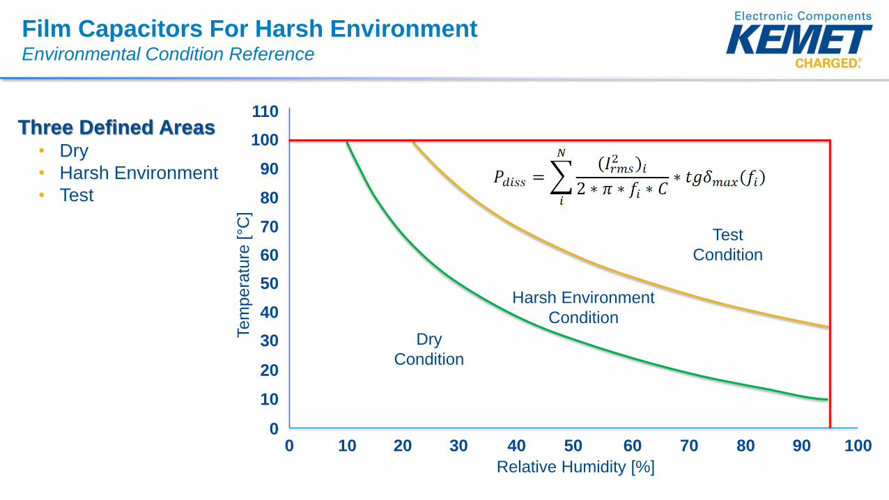
Film Capacitors For Harsh EnvironmentEnvironmental Condition Reference
Three Defined Areas• Dry
• Harsh Environment
• Test
110
100
90
80
70
60
50
40
30
20
10
0
Tem
pera
ture
[°C
]
Dry
Condition
Harsh Environment
Condition
Test
Condition
0 10 20 30 40 50 60 70 80 90 100
Relative Humidity [%]

© 2019 KEMET Corporation
Permissible Current CapabilityDry vs. Harsh Environment
Harsh EnvironmentDry

© 2019 KEMET Corporation
Life Expectancy of Film TechnologyF862 – Life vs. Temperature and Voltage

© 2019 KEMET Corporation
Manufacturing Process

© 2019 KEMET Corporation
Plastic
Raw Roll
Metallization
Slitting
Film Preparation [Wound & Stacked]
• Thermal Stability
• Thickness
• Granulation
• Electrical and Mechanical
Specifications
Film Thickness (µm)
• PP ≥ 2.4
• PET ≥ 1.2
• PEN ≥ 1.4
• PPS ≥ 1.2

© 2019 KEMET Corporation
Dielectric Film Preparation
Plastic
Raw Roll
Metallization
Slitting
• Vacuum Chamber [Resistive Evaporation]
• Zinc, Aluminum, or Zinc Alloys
• Special Profiles and Treatments

© 2019 KEMET Corporation
• High Precision
• Cutting Widths Profiles
• Film Rewinding and Storage
Dielectric Film Preparation
Plastic
Raw Roll
Metallization
Slitting

© 2019 KEMET Corporation
• Single and Multi-Winding Systems
• Fast, Slow; Hot, Cold Flattening + Heat
• Taping Protects the Sides of the Elements
• Gas Flame or Electric Arc [Thick Metal Contact]
Wound TechnologyWinding to End Spraying
Winding
Flattening
& Heat Treatment
Protective
Taping
End
Spraying
Brushing

© 2019 KEMET Corporation
• Mother Winding [Frame]
• Frame Pressing
• Contact Metal Sprayed on Both Sides
• Multi-Cut System or One Element at a Time
Stacked Technology Winding to Element Cutting
Winding
Framing Flattening
SprayingBrushing
Heat Treatment& ElementCutting

© 2019 KEMET Corporation
• Automation with Combined Tasks
• Clearing Allow Potential Self-Healing
• 100% Tested for Critical Parameters
Welding to PackagingStacked and Wound
Welding &
Clearing
Encapsulation & Resin Filling
Measuring
Quality
Marking
Packaging

© 2019 KEMET Corporation
Thank You!