final report - y17q (3) - apps.dtic.mil · mau-chung frank chang, wei-han cho, jieqiong du, yuan...
TRANSCRIPT

AFRL-RY-WP-TR-2016-0200
MULTIBAND RADIO FREQUENCY-INTERCONNECT (MRFI) TECHNOLOGY FOR NEXT GENERATION MOBILE/AIRBORNE COMPUTING SYSTEMS Mau-Chung Frank Chang, Wei-Han Cho, Jieqiong Du, Yuan Du, Sheau Jiung Lee, Yilei Li, and Chien-Heng Wong University of California, Los Angeles
FEBRUARY 2017 Final Report
Approved for public release; distribution unlimited.
See additional restrictions described on inside pages
STINFO COPY
AIR FORCE RESEARCH LABORATORY SENSORS DIRECTORATE
WRIGHT-PATTERSON AIR FORCE BASE, OH 45433-7320 AIR FORCE MATERIEL COMMAND
UNITED STATES AIR FORCE

NOTICE AND SIGNATURE PAGE
Using Government drawings, specifications, or other data included in this document for any purpose other than Government procurement does not in any way obligate the U.S. Government. The fact that the Government formulated or supplied the drawings, specifications, or other data does not license the holder or any other person or corporation; or convey any rights or permission to manufacture, use, or sell any patented invention that may relate to them.
This report is the result of contracted fundamental research deemed exempt from public affairs security and policy review in accordance with SAF/AQR memorandum dated 10 Dec 08 and AFRL/CA policy clarification memorandum dated 16 Jan 09. This report is available to the general public, including foreign nationals.
AFRL-RY-WP-TR-2016-0200 HAS BEEN REVIEWED AND IS APPROVED FOR PUBLICATION IN ACCORDANCE WITH ASSIGNED DISTRIBUTION STATEMENT.
ALFRED J. SCARPELLI BRADLEY J. PAUL, ChiefProgram Manager Advanced Sensors Components BranchAdvanced Sensors Components Branch Aerospace Components & Subsystems DivisionAerospace Components & Subsystems Division
TODD W. BEARD, Lt Col, USAFDeputyAerospace Components & Subsystems DivisionSensors Directorate
This report is published in the interest of scientific and technical information exchange, and its publication does not constitute the Government’s approval or disapproval of its ideas or findings.
*Disseminated copies will show “//Signature//” stamped or typed above the signature
SCARPELLI.ALFRED.J.1230195222
Digitally signed by SCARPELLI.ALFRED.J.1230195222DN: c=US, o=U.S. Government, ou=DoD, ou=PKI, ou=USAF, cn=SCARPELLI.ALFRED.J.1230195222Date: 2017.01.06 15:26:28 -05'00'
PAUL.BRADLEY.J.1209885146
Digitally signed by PAUL.BRADLEY.J.1209885146DN: c=US, o=U.S. Government, ou=DoD, ou=PKI, ou=USAF, cn=PAUL.BRADLEY.J.1209885146Date: 2017.01.09 15:23:36 -05'00'
BEARD.TODD.W.1140628677
Digitally signed by BEARD.TODD.W.1140628677DN: c=US, o=U.S. Government, ou=DoD, ou=PKI, ou=USAF, cn=BEARD.TODD.W.1140628677Date: 2017.01.18 16:14:10 -05'00'

REPORT DOCUMENTATION PAGE Form Approved OMB No. 0704-0188
The public reporting burden for this collection of information is estimated to average 1 hour per response, including the time for reviewing instructions, searching existing data sources, searching existing data sources, gathering and maintaining the data needed, and completing and reviewing the collection of information. Send comments regarding this burden estimate or any other aspect of this collection of information, including suggestions for reducing this burden, to Department of Defense, Washington Headquarters Services, Directorate for Information Operations and Reports (0704-0188), 1215 Jefferson Davis Highway, Suite 1204, Arlington, VA 22202-4302. Respondents should be aware that notwithstanding any other provision of law, no person shall be subject to any penalty for failing to comply with a collection of information if it does not display a currently valid OMB control number. PLEASE DO NOT RETURN YOUR FORM TO THE ABOVE ADDRESS.
1. REPORT DATE (DD-MM-YY) 2. REPORT TYPE 3. DATES COVERED (From - To)
February 2017 Final 5 November 2014 – 30 September 2016 4. TITLE AND SUBTITLE
MULTIBAND RADIO FREQUENCY-INTERCONNECT (MRFI) TECHNOLOGY FOR NEXT GENERATION MOBILE/AIRBORNE COMPUTING SYSTEMS
5a. CONTRACT NUMBER FA8650-15-1-7519
5b. GRANT NUMBER
5c. PROGRAM ELEMENT NUMBER 61101E
6. AUTHOR(S)
Mau-Chung Frank Chang, Wei-Han Cho, Jieqiong Du, Yuan Du, Sheau Jiung Lee, Yilei Li, and Chien-Heng Wong
5d. PROJECT NUMBER 1000
5e. TASK NUMBER N/A
5f. WORK UNIT NUMBER
Y17Q 7. PERFORMING ORGANIZATION NAME(S) AND ADDRESS(ES) 8. PERFORMING ORGANIZATION
REPORT NUMBER University of California, Los Angeles 420 Westwood Plaza Los Angeles, CA 90095-1594
9. SPONSORING/MONITORING AGENCY NAME(S) AND ADDRESS(ES) 10. SPONSORING/MONITORING AGENCY ACRONYM(S)
Air Force Research Laboratory Sensors Directorate Wright-Patterson Air Force Base, OH 45433-7320 Air Force Materiel Command United States Air Force
Defense Advanced Research Projects Agency/DARPA/MTO 675 N Randolph Street Arlington, VA 22203
AFRL/RYDI 11. SPONSORING/MONITORING AGENCY REPORT NUMBER(S)
AFRL-RY-WP-TR-2016-0200
12. DISTRIBUTION/AVAILABILITY STATEMENT Approved for public release; distribution is unlimited.
13. SUPPLEMENTARY NOTES This report is the result of contracted fundamental research deemed exempt from public affairs security and policy review in accordance with SAF/AQR memorandum dated 10 Dec 08 and AFRL/CA policy clarification memorandum dated 16 Jan 09. This material is based on research sponsored by Air Force Research laboratory (AFRL) and the Defense Advanced Research Agency (DARPA) under agreement number FA8650-15-1-7519. The U.S. Government is authorized to reproduce and distribute reprints for Governmental purposes notwithstanding any copyright notation herein. The views and conclusions contained herein are those of the authors and should not be interpreted as necessarily representing the official policies of endorsements, either expressed or implied, of Air Force Research Laboratory (AFRL) and the Defense Advanced Research Agency (DARPA) or the U.S. Government. Report contains color.
14. ABSTRACT The aims of this two-phase research program were to analyze, model and realize a multiband radio frequency interconnect technology (MRFI) to enable high scalability and re-configurability for inter-CPU/Memory communications with an increased number of communication channels in the frequency-domain and reduced number of physical pads/wires to accomplish higher effective bandwidth, superior energy efficiency (in terms of energy/bit) and decreased size/area of both silicon (on-chip) and PCB (off-chip) for future mobile and airborne computing systems.
15. SUBJECT TERMS multiband; RF interconnect; frequency-domain multiplexing; memory;
16. SECURITY CLASSIFICATION OF: 17. LIMITATION OF ABSTRACT:
SAR
8. NUMBER OF PAGES 104
19a. NAME OF RESPONSIBLE PERSON (Monitor) a. REPORT Unclassified
b. ABSTRACT Unclassified
c. THIS PAGE Unclassified
Alfred Scarpelli 19b. TELEPHONE NUMBER (Include Area Code)
N/A Standard Form 298 (Rev. 8-98)
Prescribed by ANSI Std. Z39-18

iApproved for public release, distribution is unlimited.
Table of Contents
Section Page
List of Figures ................................................................................................................................ iii List of Tables ................................................................................................................................ vii 1. ACKNOWLEDGEMENT....................................................................................................... 1 2. EXECUTIVE SUMMARY..................................................................................................... 2 3. INTRODUCTION................................................................................................................... 4 4. METHODS, ASSUMPTIONS, AND PROCEDURES .......................................................... 9
4.1 Phase I (Five-Band QPSK Parallel Link) ........................................................................... 9 4.1.1 Differential Mode Signaling ..................................................................................... 9 4.1.2 TX and RX Designs ................................................................................................ 11 4.1.3 VCO Design and Calibration Algorithm ................................................................ 12 4.1.4 Phase Synchronization and Implementation........................................................... 17 4.1.5 One-byte MRFI bus designed with five carriers and QPSK modulation................ 20 4.1.6 TX/RX Path ............................................................................................................ 21 4.1.7 Physical Interconnect Emulations........................................................................... 22 4.1.8 TX Design and Layout............................................................................................ 22 4.1.9 TX/RX Design and Layout ..................................................................................... 23 4.1.10 Frequency Carrier Generation................................................................................. 25 4.1.11 Wide-Tuning-Range, Low-Jitter PLL Design ........................................................ 26 4.1.12 VCO design............................................................................................................. 27 4.1.13 Frequency Band Selection and Process Tracking................................................... 27 4.1.14 Divider Design ........................................................................................................ 28 4.1.15 Phase-Frequency Detector Design.......................................................................... 28 4.1.16 Charge Pump and Loop Filter Design .................................................................... 28 4.1.17 Phase Delay Correction Algorithm......................................................................... 29
4.2 Phase II (Tri-Band 16QAM Parallel Link) ....................................................................... 29 4.2.1 Self-Equalization of Double-Sideband Signaling................................................... 34 4.2.2 Transceiver System Analysis and Design............................................................... 36 4.2.3 Circuit Design of Tri-Band PAM-4 / 16-QAM Transmitter................................... 41 4.2.4 Circuit Design of Dual-Band Carrier Generator ..................................................... 43 4.2.5 Circuit Design of Tri-Band PAM-4 / 16-QAM Receiver ....................................... 44 4.2.6 Circuit Design of 4-Lane Transceiver with Built-In Self-Testing (BIST).............. 47
4.3 Development of MRFI Serial Links ................................................................................. 49 4.3.1 TX Design for MRFI Serial Links .......................................................................... 51 4.3.2 Channel Responses with Frequency Notches ......................................................... 53 4.3.3 Phase Calibration and Phase Recovery for Serial Interface.................................... 55 4.3.4 Link Budget Calculation and Clock Forwarded Architecture ................................ 57 4.3.5 Circuit Design Cognitive Tri-Band Transmitter Building Blocks.......................... 58 4.3.6 MRFI Serial Link Receiver Design ........................................................................ 60 4.3.7 Receiver Clock Recovery and Sample Timing Optimization................................. 62 4.3.8 Inter-band Interference and the Cancellation Algorithm........................................ 64 4.3.9 Circuit Design of Multi-Band RF Receiver Analog Front-End.............................. 67

iiApproved for public release, distribution is unlimited.
Section Page
4.4 Receiver Front-End Die Photo and Post-Layout Simulation............................................ 69 4.5 Benchmarking with State-of-the-Art ................................................................................ 70
5. RESULTS AND DISCUSSIONS ......................................................................................... 72 5.1 Phase-I Test Results and Benchmarking with State-of-the-Art ........................................ 72 5.2 Phase-II Test Results and Benchmarking with State-of-the-Art....................................... 77 5.3 MRFI Serial Link Performance Summary........................................................................ 81
5.3.1 TX Test Results and Benchmark with State-of-the-Art.......................................... 81 5.3.2 RX Test Results and Benchmark with State-of-the-Art ......................................... 85
6. CONCLUSION ..................................................................................................................... 88 7. REFERENCES...................................................................................................................... 89 LIST OF ACRONYMS, ABBREVIATIONS, AND SYMBOLS ............................................... 92

iiiApproved for public release, distribution is unlimited.
List of Figures
Figure Page
Figure 1: Exemplary Nth Processor with Eight Concurrent Memory Buses (256Bit/Bus) ............ 5 Figure 2: Parallel Byte Bus (10Bit) Transmitted and Received Simultaneously via Multiple Frequency Carriers.......................................................................................................................... 6 Figure 3: MRFI with Self-Track Pulse Generator and Restoration for I/O Data Synchronization ............................................................................................................................ 10 Figure 4: Direct Current Reduction Circuit with Process Variation Track ................................. 11 Figure 5: Differential Current Steering Mixer with Quarter Duty Cycle Carrier ........................ 12 Figure 6: Voltage Control Oscillator ........................................................................................... 13 Figure 7: CML Inverter Chain ..................................................................................................... 14 Figure 8: CML Inverter with Programmable Resistor................................................................. 15 Figure 9: Self-Calibration Controller........................................................................................... 16 Figure 10: Flow Chart of Calibration Controller ......................................................................... 17 Figure 11: Circuit Blocks for Phase Adjustment ......................................................................... 18 Figure 12: Flow Chart for Phase Adjustment .............................................................................. 19 Figure 13: Block Diagram of One-Byte MRFI by Five Frequency Carriers and QPSK Modulation.................................................................................................................................... 20 Figure 14: Multi-band QPSK RF-Interconnect Channel Spectrum............................................. 21 Figure 15: Layout of MRFI Test Chip in 40nm Technology....................................................... 21 Figure 16: TX/RX Path in the Full-Chip Layout ......................................................................... 22 Figure 17: Layout of the Interconnect Emulator.......................................................................... 22 Figure 18: Layout of the Five-Band QPSK Transmitter.............................................................. 23 Figure 19: TX Output Current Spectrum in Typical/Worst / Best Cases and SF/FS Corners..... 23 Figure 20: Layout of the Five-Band QPSK Receiver .................................................................. 24 Figure 21: Frequency Response of Current Gain and Group Delay of the Current-Mode LPF.. 24 Figure 22: Carrier Generation in the Full Chip Layout ............................................................... 25 Figure 23: Carrier Generation Block Diagram ............................................................................ 25 Figure 24: Blocks in the Layout of Carrier Generation ............................................................... 26 Figure 25: PLL Layout................................................................................................................. 27 Figure 26: PLL Block Diagram ................................................................................................... 27 Figure 27: Ring Oscillator VCO.................................................................................................. 27 Figure 28: Band Selection Algorithm Flow Chart ....................................................................... 27 Figure 29: Free-Run Frequency of VCO (a) Without and (b) With Process Track..................... 28 Figure 30: Received Constellation (a) Without and (b) With Phase Error .................................. 29 Figure 31: Phase Adjustment Algorithm Flow Chart .................................................................. 29 Figure 32: Tri-Band Signaling in Time and Frequency Domain, and Comparison with NRZ Signaling ....................................................................................................................................... 31 Figure 33: NRZ Signaling with Channel Frequency Notches ..................................................... 31 Figure 34: PAM-4 / 16-QAM Tri-Band Signaling with Channel Frequency Notches................ 32 Figure 35: NRZ Signaling with Monotonic Channel Attenuation............................................... 32 Figure 36: PAM-4 / 16-QAM Tri-Band Signaling with Monotonic Channel Attenuation ......... 33 Figure 37: (a) Self-Equalization and (b) DSB Signaling Output Eye Diagram........................... 34

ivApproved for public release, distribution is unlimited.
Figure Page
Figure 38: (a) I/Q Interference of Quadrature Modulation due to Uneven Channel Attenuation; (b) Folded Waveform of I/Q Interference in Time-Domain; (c) Degraded Output Eye Diagram due to I/Q Interference................................................................................ 35 Figure 39: (a) Example of Channel Frequency Response with Slope of -20dB/dec; (b) Effective I/Q Transfer Functions Derived from the Example; and (c) Peaking/Interference of the Transfer Functions .............................................................................................................. 36 Figure 40: Dual-DIMM Multi-Drop Memory Bus and Analysis of Induced Frequency Notches ......................................................................................................................................... 37 Figure 41: (a) Adjacent-Band Interference Analysis; (b) Folded Waveform of the Remaining Interference; (c) the Eye Diagram of the Demodulated Signal from 6GHz Band........................ 38 Figure 42: Output Eye Diagram of the PAM-4 / 16-QAM Tri-Band Signaling and Constellation of 3GHz and 6GHz Bands ...................................................................................... 39 Figure 43: Phase Noise Shaping of Synchronous Signaling and its Effect on Carrier Jitter ....... 39 Figure 44: Bit Error Rate and Jitter Requirement Calculation of 16-QAM ................................ 41 Figure 45: Transmitter Block Diagram of Tri-Band PAM-4 / 16-QAM Signaling..................... 42 Figure 46: Circuit Schematic of One Modulation Path in the Tri-Band Transceiver .................. 42 Figure 47: Block Diagram of the Dual-Band I/Q Carrier Generator ........................................... 43 Figure 48: Receiver Block Diagram of Tri-Band PAM-4 / 16-QAM Signaling ......................... 44 Figure 49: Circuit Schematic of the Gain-Reused Regulated Cascade Input Buffer................... 45 Figure 50: Simulated S11 Frequency Response of the Gain-Reused Regulated Cascade Input Buffer................................................................................................................................... 45 Figure 51: Circuit Schematic of One Demodulation Path in the Tri-Band Transceiver.............. 46 Figure 52: Block Diagram of the 3rd-Order Bessel Gm-C Low-Pass Filter ................................ 46 Figure 53: Illustration of the Transceiver Testing Environment with Built-In Self-Tester ......... 47 Figure 54: 32-bit PRBS Generator Implemented with Reversely Combined Linear Feedback Shift Registers (LFSRs) ................................................................................................................ 48 Figure 55: Illustration of the Transceiver Testing Environment with Built-in Self-Testing ....... 49 Figure 56: System Architecture of a Typical NRZ Serial Link ................................................... 50 Figure 57: Conceptual Multi-Band Serial Links.......................................................................... 51 Figure 58: Self-Equalization of Direct-Conversion Multi-Band Links [7] ................................. 51 Figure 59: System Architecture of Cognitive Transmitter with Multi-Band Signaling and Channel Learning Mechanism ...................................................................................................... 52 Figure 60: (a) Common Periphery Serial Link; (b) Cable-Only and Complete Channel Insertion Loss; (c) With and Without MDB Insertion Loss ......................................................... 53 Figure 61: Memory Controller with Two DIMMS per Channel ................................................. 54 Figure 62: Time-Domain Single-Bit Response............................................................................ 54 Figure 63: Conceptual Comparison of Baseband TX and Multi-Band TX ................................. 54 Figure 64: Baseband TX vs Multi-Band TX on Multi-Drop Memory Interface Channel........... 55 Figure 65: Phase Offset Impact on Data Eye Quality.................................................................. 56 Figure 66: Proposed Phase Calibration Scheme with One-Bit ADC........................................... 57 Figure 67: Link Budget Calculation ............................................................................................ 57 Figure 68: Conventional Source-Synchronized / Forward Clocking Architecture...................... 58 Figure 69: Digital-to-Analog Convertor and Mixer Schematics ................................................. 58 Figure 70: 10 Five-Slice Summation Block Schematics ............................................................. 59

vApproved for public release, distribution is unlimited.
Figure Page
Figure 71: Fully Reconfigurable Receiver Front End Schematics .............................................. 59 Figure 72: Embedded Forwarded Clock ...................................................................................... 62 Figure 73: SIR vs Sampling Timing ............................................................................................ 63 Figure 74: Sampling Timing Calibration Circuit Block Diagram and Flow Chart ..................... 63 Figure 75: Inter-band Interferences in Frequency Domain.......................................................... 64 Figure 76: System Operation Flow.............................................................................................. 65 Figure 77: Constellation and Eye Diagram With and Without Inter-Band Interference Cancellation .................................................................................................................................. 66 Figure 78: Transient Response With and Without Inter-Band Interference Cancellation........... 66 Figure 79: Programmable Receiver Input Buffer Schematic....................................................... 67 Figure 80: Simulated Input Impedance for Programmable Receiver Input Buffer ..................... 68 Figure 81: Mixer and Low-Pass Filter Schematics...................................................................... 68 Figure 82: Linearized Transconductance (Gm) Cell for Low-Pass Filter ................................... 69 Figure 83: Die Photo and Layout of Receiver Front-End............................................................ 69 Figure 84: Eye Diagram and Constellation of Post Layout Simulation....................................... 70 Figure 85: Channel Spectrum of the FDM Memory Interface with Five-Band QPSK Modulation.................................................................................................................................... 72 Figure 86: Illustration of Self-equalized QPSK Modulation ....................................................... 72 Figure 87: Block Diagram of the Five-Band QPSK Transceiver ................................................ 73 Figure 88: Schematics of the Differential Current-Steering DAC and the Receiver Input ......... 74 Figure 89: Schematics of the Current-Mode Low-Pass Filters and the Current-Mode Schmitt Trigger ............................................................................................................................. 74 Figure 90: Micrograph of the Test Chip with Both TX/RX and 1-pF On-Chip Interconnection to Emulate TSV Loading in 3DIC .................................................................................................... 75 Figure 91: (a) Demodulated 400-Mb/s 231-1 PRBS Eye Diagrams of I/Q Channels at f1 (Upper) and f2 (Lower); (b) 250-Mb/s 231-1 PRBS Eye Diagrams of Original (Upper) and Demodulated (Lower) DQ/DQS ............................................................................................ 75 Figure 92: Top View of the Test Board with Separate TX/RX Connected with a 5-cm FR-4 Differential Trace................................................................................................................. 75 Figure 93: (a) Demodulated 400-Mb/s 231-1 PRBS Eye Diagrams of the 1-cm (Upper) and the 5-cm (Lower) Test Boards; (b) Latency of 2.4 ns Found by Subtracting Out Measured Cable Delay (Upper) from Measured Total Delay (Lower, Output Inverted) ............. 76 Figure 94: Real-Time Flexible BER Testing Platform for Five-Band QPSK Transceiver ......... 76 Figure 95: Die Photo of the Four-Lane Tri-Band Transceiver with Built-In Self-Tester............ 77 Figure 96: Testing Environment and the Test Board with 2-Inch Dense FR-4 Differential Bus ................................................................................................................................................ 78 Figure 97: Measured Output Eye Diagram and Transient Waveform......................................... 78 Figure 98: Transmitter Output Spectrum and Energy Efficiency vs Channel Attenuation ......... 79 Figure 99: Power Breakdown of the Four-Lane Tri-Band Transceiver....................................... 79 Figure 100: Measurement Platform ............................................................................................. 81 Figure 101: Time-Domain Measurement Results........................................................................ 81 Figure 102: Frequency-Domain Measurement Results ............................................................... 82 Figure 103: Cognitive Algorithm Description............................................................................. 83 Figure 104: Die Photo of Cognitive Tri-Band Transmitter ......................................................... 84

viApproved for public release, distribution is unlimited.
Figure Page
Figure 105: Power Consumption Breakdown.............................................................................. 84 Figure 106: Die Photo and Layout of MRFI Serial Link RX Front-End..................................... 85 Figure 107: Measurement Platform ............................................................................................. 86 Figure 108: Measurement Results (Eye Diagram and Constellation) ......................................... 86 Figure 109: Power Consumption Breakdown.............................................................................. 87

viiApproved for public release, distribution is unlimited.
List of Tables
Table Page
Table 1. Targeted MRFI Specification .......................................................................................... 3 Table 2. Comparison of MRFI with State-of-the-Art Counterparts .............................................. 7 Table 3. ADC Resolution Specs of Phase Calibration for Different Modulation Schemes ........ 56 Table 4. MRFI Serial Link Performance Metrics ........................................................................ 60 Table 5. Benchmarking with State-of-the-Art ............................................................................. 71 Table 6. Benchmarking with State-of-the-Art ............................................................................. 80 Table 7. Benchmarking MRFI Serial Link TX Performance with State-of-the-Art.................... 85

1Approved for public release, distribution is unlimited.
1. ACKNOWLEDGEMENT
The authors would like to thank Taiwan Semiconductor Manufacturing Company (TSMC) for chip fabrication, Minji Zhu for help of assembling and testing in the University of California, Los Angeles (UCLA) Center for High Frequency Electronics, and Dr. Afshin Momtaz at Broadcom Corporation for valuable advice and technical discussions on the high-speed wireless implementation. The authors would also like to thank Janet Lin for proofreading and editing the final technical report.

2Approved for public release, distribution is unlimited.
2. EXECUTIVE SUMMARY
The aims of this two-phase research program were to analyze, model and realize a multiband radio frequency interconnect technology (MRFI) to enable high scalability and re-configurability for inter-central processing unit (CPU)/Memory communications with an increased number of communication channels in the frequency-domain and reduced number of physical pads/wires to accomplish higher effective bandwidth, superior energy efficiency (in terms of energy/bit) and decreased size/area of both silicon (on-chip) and printed circuit board (PCB) (off-chip) for future mobile and airborne computing systems.
The goal of Phase I (6 months) was to quickly validate the functionality of all complementary metal oxide semiconductor (CMOS) building blocks (including digital to analog converter (DAC), analog to digital converter (ADC), Modulator, de-Modulator, Oscillators, phase lock loops (PLL), Track Pulse Generator/Restorer) and the data access and transfer operations of the entire byte of data (containing 8 bit of data, 1 bit of byte mask, 1 bit of data strobe) simultaneously by using 5 frequency carriers (1.6GHz, 2.4GHz, 3.2GHz, 4GHz, and 5.2GHz) and Quadrature Phase Shift Keying (QPSK) modulation, for verifying its effective bandwidth, energy efficiency, latency, etc. We successfully delivered a 1-Byte MRFI Bus prototype by using 40nm CMOS technology according to the performance specs listed in the 2nd column of Table 1.
In Phase II (12 months), we taped out One Full Channel (4-Byte or 32bit data, 4 bit of byte mask, 4 bit of data strobe) MRFI Physical Layer (PHY) based on Taiwan Semiconductor Manufacturing Company (TSMC) 28nm CMOS technology. The 4-Byte MRFI PHY was designed by using more energy/area-efficient 16 quadrature amplitude modulation (QAM) signal modulation and 2 frequency carriers (two frequency carriers at 1.2GHz and 2.4GHz, respectively) in addition to the baseband for achieving even higher energy efficiency (<0.5pJ/bit) and smaller Input/Output (I/O) die area. We again successfully delivered a Full Channel 4-Byte MRFI PHY on 28nm CMOS technology according to the performance specs listed in the 3rd
column of Table 1.
In addition to developing the aforementioned MRFI PHY for parallel interconnect links primarily applicable to multi-byte communications between CPU and memories, we also evaluated MRFI serial links for integrating heterogeneous die on high performance interposer. Aserial link transmitter in 28nm CMOS technology was developed with simultaneous high-speed (34Gbps) and high-efficiency (pJ/bit) by using 3-bands (2-carriers/1-baseband) and up to 256QAM modulation. A corresponding serial link receiver was also developed by using the same number of carriers and modulation schemes.

3Approved for public release, distribution is unlimited.
Table 1. Targeted MRFI Specification
Phase I Phase IIIntegration scale 1 byte TX/RX 4 byte PHY TX/RXNumber of frequency carriers 5 2Frequency selected 1.6/2.4/3.2/4/5.2GHz 1.2/2.4GHzModulation QPSK QAM16Number of bit per byte 10 10Data clock rate 200MHz 300MHzTarget peak bandwidth of 2048 bit memory bus
409.6 Gbit/s 614.4 Gbit/s
Target I/O current per pair 1.8 ma 0.9 maTarget I/O current per bit 0.18 ma 0.09 maTarget I/O power per bit < 1 pJ/bit <0.5pJ/bitLatency of PHY delay < 3 ns < 4.5 nsProcess node 40nm (TSMC) 28nm (TSMC)Supported memory channel NA 1 Channel Area per bit in PHY 900 um2 (40nm) 350 um2 (32nm)

4Approved for public release, distribution is unlimited.
3. INTRODUCTION
The advancement of modern massive parallel computing relies on innovative development of multi-core CPUs and effective interconnects that can link multi-core CPUs with various caches and memories. Advanced mobile and/or airborne computing platforms have even more complicated issues than those of typical computing systems: their power consumption must be minimized while still offering high data rate and low latency to support multi-functional system applications. In addition to data processing, the memory bandwidth required by multi-graphics processing unit (GPU)/accelerated processing unit (APU) applications is equally demanding. These obstacles call for the need for mobile/airborne platforms to be implemented by using an interconnect system (in both architecture and technology) that can facilitate not only higher bandwidth, lower latency, and lower power consumption but also with more competitive production cost.
The conventional memory hierarchy of high speed computing systems suffers serious constraints from its latency, bandwidth and power consumption due to conventional time-domain multiplexing techniques such as Low Power Double-Data-Rate (LPDDR). For instance, the size of the on-chip cache is limited to 128Mbyte due to processing yield problems of integrating memories with Application-Specific Integrated Circuits (ASIC). The memory bus width and memory channels are also limited, respectively, owing to excessive power dissipation from large number of chip interconnects with high speed signaling and clocking. To overcome such technical barriers, we proposed to develop a novel MRFI interconnect technology by using multiband concurrent signal processing through shared physical wires (either traditional T-lines or advanced through-silicon vias (TSV) to revolutionize future inter-CPU/Memory interconnect technology with the highest bandwidth, lowest latency, lowest energy/bit (by factor 10 lower than that of existing LPDDR) and the lowest packaging cost (compatible with traditional low cost 2D Fine Pitch Ball Grid Array (FBGA) and high performance 2.5D Interposer and 3DIC). Such an interconnect scheme is not only more scalable than state-of-art technologies due to its use of multiband and QAM communications but also more reconfigurable by using software programming for load balance among all communication channels. Our proposed interconnect scheme would enable performance/ energy/ cost-effective connectivity to both on and off-chip larger size caches, and to wider memory bus with larger number of concurrent memory channels, without paying penalties to accessing latency, power consumption, or production yield/cost.
Figure 1 shows the designed high performance computing node in multi-core massive parallel computing systems based on our proposed MRFI. Figure 2 shows a concurrent multi-bit byte bus which can simultaneously access and transfer 10 bits (8 bits of data, 1 bit of byte mask and 1 bit of data strobe) by using multiple frequency carriers with separate in phase and quadrature phase(I/Q) modulations.

5Approved for public release, distribution is unlimited.
Figure 1: Exemplary Nth Processor with Eight Concurrent Memory Buses (256Bit/Bus)
Figure 2 shows a concurrent multi-bit byte bus which can simultaneously access and transfer 10 bits (8 bits of data, 1 bit of byte mask and 1 bit of data strobe) by using multiple frequency carriers with separate I/Q modulations. The modulated signal will be transmitted through differential pair of wires between CPUs and memories, and then demodulated by the same frequency carriers to restore the data back to a parallel bus. This implies that one can reduce the number of interconnects in Wide-input/output (I/O) by a factor X5. In this exemplary system, one only uses 892 interconnects for communicating 4096 I/O signals. Furthermore, MRFI PHY (i.e. transceivers) will operate under current steering logic over a differential pair circuitry. This can also reduce the simultaneous switching noise (SSN) problem to several orders-of-magnitude lower than that of competing Wide-I/O where large rail-to-rail CMOS logic swings are being used.

6Approved for public release, distribution is unlimited.
Figure 2: Parallel Byte Bus (10Bit) Transmitted and Received Simultaneously via Multiple Frequency Carriers
Furthermore, since MRFI modulates bus data in frequency domain and traditional transmission line problems only occur on its carriers and not on its low frequency data, it is therefore more forgiving in choosing its packaging types and does not require costly 3DIC as that of Wide-I/O. This allows us to deploy MRFI PHY over low cost conventional FBGA packaging technologies. This also shows that we can solve most Wide-I/O problems and retain its performance with even lower power consumption (X5 according to simulations) as well as with lower cost production.
One differential
pair of wires

7Approved for public release, distribution is unlimited.
MRFI Performance Benchmarking
Table 2. Comparison of MRFI with State-of-the-Art Counterparts
LPDDR4 (Intel and
others)
Wide I-O(Samsung)
R+LPDDR3 (RAMBUS) MRFI
Signal type Single-ended voltage mode
Single-ended voltage mode
Single-ended voltage mode
Differential current mode
Voltage swing 400mv center Vtt=Vdd/2
1.2V rail-to-rail
300mv near ground
differential +/-15mv with common mode
Signal toggling rate 3.2GHz 0.2GHz 3.2GHz0.3GHz with carrier modulation
TerminationParallel vtt -terminated at 50ohm
un-terminated
parallel ground-terminated 50 ohm
un-terminated (leads to no power dissipation by terminators)
Minimum I/O drive per I/O signal >8ma >0.8 ma >6ma 0.8ma (pair)
Maximum loading 5PF 1PF 5PF 1PFNumber of signals in I/O interface 76 (2ch) 773 (4ch) 76 (2ch) 75 pair (4ch)
Minimum interface current >608 ma >678 ma >456 ma 60 ma
Interface SSN with (1nH) parasitic
1.94V (serious aggressor)
0.136v(possible aggressor)
1.46v (serious aggressor)
0.001v (not aggressor)
Required Power-ground to combat SSN
>140 >427 >140 >33 pair
Minimum interface Pads >216 pads >1200 TSV >216 pads 216 pads
PHY size with pads or TSV
216 *(45*450) 28lp ~5X
1200*(45*90) 28lp ~5X
216*(45*450) 28lp ~5X
216*45*90 28lp ~1X
Package type
PoP, discrete Package, 256 FBGA (14mmx14mm) for dual channels
3DIC
PoP, discrete Package, 256 FBGA (14mmx14mm) for dual channels
PoP, discrete package, 216 FBGA for quad channels, 3DIC
Number of channel per device 2 4 2 4
Time Multiplex: Demultiplex 8:1 / 1:8 NA 8:1 / 1:8 NA

8Approved for public release, distribution is unlimited.
Required skewadjust for each DQ/DQS
yes no yes no
Write leveling required NA required NACA Training required NA required NA
Latency in TX PHY for Mux, skew adjustment, fly time
>4 ns (8 clk of 3.2GHz, PCB fly time)
5 ns (register delay)
>4 ns (8clk of 3.2GHz, PCBfly time)
1.2 ns (DAC, Modulation delay, PCB fly time)
Latency in RX PHY for demux, skew, byte/word align, fly time
>6 ns (DLL adjust, align, demux)
5 ns (register delay)
>6 ns (DLL adjust, align, demux)
1.8 ns(demodulation, Low pass filter)
Total latency of TX/RX PHY >10 ns >10 ns >10 ns 3 ns
Peak bandwidth per device
102.4Gb/s at 3.2Ghz toggle
102.4Gb/s at 0.2GHz toggle
102.4Gb/s at 3.2Ghz toggle
153.6Gb/s at 0.3Ghz toggle with modulation
Effective bandwidth for short burst transfer (<32 burst)
Low Low Low High
Effective bandwidth for locality (e.g. streaming)
Low (2ch) High (4ch) Low (2ch) High (4ch)
MRFI multiplexes data in-parallel through the frequency domain instead of in-serial through the time domain. This avoids high speed data/clock toggling and consequent high power consumption. This also avoids timing adjustment-related latency for matching data strobe signal (DQS)/output data (DQ) traces. As a result, MRFI is able to support a very wide data bus with very short latency and low power consumption.

9Approved for public release, distribution is unlimited.
4. METHODS, ASSUMPTIONS, AND PROCEDURES
4.1 Phase I (Five-Band QPSK Parallel Link)
In Phase I, we aimed to analyze, model and implement the designed MRFI to enable high scalability and reconfigurability for inter-CPU/Memory communications with an increased number of communication channels in frequency-domain and a reduced number of physical pads/wires to obtain higher effective bandwidth, superior energy efficiency (in terms of energy/bit) and decreased size/area of both silicon (on-chip) and PCB (off-chip) for future mobile and airborne computing systems. Our methods are listed below:
4.1.1 Differential Mode Signaling
We exploited a novel innovative differential current mode modulation/demodulation method to achieve shorter latency, lower power, and resilience to process variations for multi frequency band QAM transceiver circuits to make the method possible to become the foundation for MRFI. The invention achieves shorter latency delay and lower power consumption with higher yield manufacturing. It also includes a DC current reduction circuit element to improve the signal-to-noise ratio. The proposed circuits were all implemented by using current mirrors with proven higher manufacturing yield. A current mode Schmitt Trigger with adjustable hysteresis value was included in the demodulation circuit to improve data recovery without creating bit error.
The modulation and demodulation circuit (Figure 3) consists of two parts: the modulation circuit performs transmission (TX) while the demodulation circuit performs reception (RX). The modulation circuit includes digital-to-analog converter and mixer. The demodulation circuit includes mixer and analog-to-digital converter. The circuit transmits one byte of digital signal after applying multi frequency modulation and combines all output of mixer and then transmits from TX. The circuit receives a byte of digital signal by applying the same multi frequency to demodulate the combined signal from TX and then generating the receiving digital signal in byte.

10Approved for public release, distribution is unlimited.
Figure 3: MRFI with Self-Track Pulse Generator and Restoration for I/O Data Synchronization
The circuit transmits the differential current signal after converting the digital voltage signal by the digital-to-analog converter. The differential current signal will be modulated by applying a defined frequency carrier which is in voltage control signal. The differential current signal being modulated by mixer will be combined before TX sends the combined signal through connection pins. The circuits receive the differential current signal from TX, which will be sent to mixer for demodulation. A circuit performs direct current reduction to improve the signal ratio and reduce the power consumption before sending the receiving differential current signal directly to all mixers. Figure 4 shows this direct current reduction circuit.

11Approved for public release, distribution is unlimited.
Figure 4: Direct Current Reduction Circuit with Process Variation Track
The reduced direct current will remove any extra direct current to ensure the sum of the differential current to mixer equals 10*I_C. This circuit also shows that the amount of direct current removed changes as I_P and I_N changes to ensure the sum of input to mixer remains constant. The constant differential current signal allows a consistent circuit behavior of mixer.
4.1.2 TX and RX Designs
To transmit the data, the modulation circuit uses a differential current mode digital-to-analog converter. Once the digital signals are converted into differential current signal, this differential signal is modulated by current mode mixer. Figure 5 shows the mixing carrier being a quarter duty cycle of digital steering signal, which can be used to avoid the interference between I-channel and Q-channel. A four phase mixing carrier can be implemented to keep fast current steering to avoid starvation of current in the differential pair. The four phase carrier operates as follows: during phase P_0, CLK_P and CLKN_N are high to make (I_MIX_P = I_DAC_P, I_MIX_N=I_DAC_N). Phase 0 produces the differential current signal in the same phase of current mode DAC output. During phase 1, CLKN_P and CLKN_N are high to make [I_MIX_P= I_MIX_N=0.5*(I_DAC_P + I_DAC_N)]. Phase 1 produces the differential current signal to be zero. During Phase 2, CLK_N and CLKN_P are high to make (I_MIX_P=I_DAC_N, I_MIX_N=I_DAC_P). Phase 2 produces the differential current signal in 180 degrees of current mode DAC output. During phase 3, CLKN_P and CLKN_N are high to make [I_MIX_P= I_MIX_N=0.5*(I_DAC_P + I_DAC_N)]. Phase 3 produces the differential

12Approved for public release, distribution is unlimited.
signal to be zero. Current will not turned off at any given time, thus avoiding current spike and reducing unexpected noise during mixing. The direct current level allows the mixer to operate at high frequency without serious degradation.
Figure 5: Differential Current Steering Mixer with Quarter Duty Cycle Carrier
In the transmission circuit, the out pin of TX will drive the signal from the sum of output signals. Because the signal is in differential current mode, one can wire all output current mirrors directly after the mixer. This differential current signal is then passed to RX which implements a direct current reduction circuit to reduce the direct current level to the predefined level. The residual differential current signal will be sent to the demodulation mixer. After demodulation, a low pass filter can be used to filter out adjacent frequency band signal. An analog-to-digital converter can be used to restore the digital signal from the analog signal.
The signal (after low pass filter) carries adjacent channel interference, generating a ripple. To ensure the robust operation with the presence of the unwanted ripple, a hysteresis can be applied in the ADC to prevent the incorrect signal generation. Because this is differential current signal, the amount of hysteresis can be digitally programmed through the current mirror in the comparators of the ADC.
4.1.3 VCO Design and Calibration Algorithm
Tunable voltage control oscillator (VCO) is the key circuit block for frequency synthesizer and phase lock loop in the MRFI connection. A good tunable VCO with low jitter can improve the system performance greatly. The frequency gain by control voltage (KVCO) should be kept as

13Approved for public release, distribution is unlimited.
small as possible over the target tuning frequency range to obtain the low jitter performance in VCO. However, the KVCO needs to be increased to cover not only the target tuning frequency range but also the chip fabrication process variation. The typical variation is about 50% between slow-slow process corner and fast-fast process corner so if the VCO is designed with 20% frequency tuning range, the KVCO must cover 70% tuning range. As a result, unnecessary high KVCO causes large jitter of VCO.
We implemented a tunable VCO that can compensate for the process variation through self-calibration circuits which can reduce the large fabrication process variation and allows the implementation of a VCO with low KVCO to cover the target tuning range and avoid unnecessary large KVCO. This implementation of VCO can optimize the jitter for a given target tuning range and cover wide chip fabrication process. The self-calibration circuits inside the chip is realized by an implementation of feedback control circuits to create a constant resistor-capacitor (RC) delay for each stage of current mode inverter inside VCO even as the process changes. Even with variation due to the process change, the feedback control circuit will prevent the KVCO characteristic of VCO from changing. The reduction of RC delay variation will reduce the variation of oscillation frequency in VCO.
The uniqueness of this VCO is that the automatic feedback circuits emulate the external constant device which reduces the variation caused by the fabrication process variation. This invention not only optimizes the performance for a given process but also allows the design to betransferred to different foundries.
The VCO (Figure 6) consists of 4 parts: Part1 is a circuit of vct_2_pct gain buffer amplifying VCT from low pass filter to P_CNT that changes the resistance of positive metal-oxide semiconductor (PMOS) and current in current mode logic (CML) inverter. By varying P_CNT, CML inverter can operate with different delay time as P_CNT changes. When P_CNT fully turns on PMOS to increase the current in CML inverter to a maximum, CML inverter will operate at the shortest delay time. When P_CNT fully turn off PMOS to reduce the current in CML inverter to a minimum, CML inverter will operate at the longest delay time. The control pin, CALI_N, will provide the control mechanism to the self-calibration controller during the calibration operation.
Figure 6: Voltage Control Oscillator

14Approved for public release, distribution is unlimited.
Part2 is a circuit of pct_2_vct that keeps the constant voltage swing for CML inverter during P_CNT changes. The voltage swing of CML is equal to product of current and resistance of the loaded device. When P_CNT changes to reduce the resistance of load device in CML inverter in order to increase speed, Part2 circuit will generate more current to CML inverter such that voltage swing is maintained as a constant. This circuit ensures the same operating point of circuit so that all parasitic contribution to circuit operation is the same even when P_CNT changes.
Part3 is a circuit of resistor emulation. Figure 7 shows that an external resistor outside the chip is tied to power supply. An external current source is applied to the circuit. With these two external components, the internal loaded device of CML inverter can be programmed to track with fabrication process variation. This circuit has 6 bits of programming control that can be used by the self-calibration controller to control the based current under the fixed voltage swing.
Figure 7: CML Inverter Chain
The circuits show the oscillator consisting of a chain of several stages of CML inverters. Each stage of CML inverter has a delay of Td. The amount of Td is dependent on C*Swing/current, where C is total node capacitance, swing is the difference of highest voltage and lowest voltage in the oscillation wave form, and current is the current supplied to each CML inverter. Since the swing is fixed by the circuits in part2 and part3 and the node capacitance is fixed by the device size, the current supplied to CML inverter changes as N_CNT changes to track P_CNT and P_CNT is amplified from VCT, voltage to control the VCO frequency. Changing VCT will change current and Td, and once Td changes, the VCO frequency changes. The VCO frequency is proven to be inversely proportional to twice the sum of Td in each stage of the chain.
Thus if the voltage swing is kept constant in spite of process changes, the current can be programmed by part3 circuit to compensate for the capacitance loading changes due to process variation. By such calibration, the design of KVCO for VCO can be greatly minimized for a given tuning range because the process variation can be compensated. As a result of low KVCO, the design can achieve the low jitter for VCO.
Figure 8 shows the detailed circuit in transistor level to implement part2 and part3 along with tracking CML inverter. The CML inverter shown consists of two loaded devices, two switch NMOS and two current source n-channel metal-oxide semiconductor (NMOS). The loaded devices consist of three parallel circuit elements: one poly resistor, one PMOS for compensating process variation, and one PMOS for tuning frequency. Two current source NMOS, a fixed current that is programmed to compensate the process variation and one that changes as P_CNT

15Approved for public release, distribution is unlimited.
changes to keep the voltage swing constant, will tune the frequency of VCO over its tunable range.
Figure 8: CML Inverter with Programmable Resistor
P_CNT is pulled to VDD when the low pass filter pulls VCT close to VDD. Then the resistance of the loaded device of CML inverter changes to maximum because the PMOS is turned off. In this case, N_CNT will cut off the current shown in Figure 8. As a result, CML inverter always operates with the same voltage swing at the highest resistance and lowest current source. One can assure that CML operates at its lowest possible oscillating frequency under this condition. Figure 8 further shows that combining part2 and part3 circuit by the operation bias will remain the same during P_CNT changes to tune the VCO frequency.
When P_CNT turns off the PMOS, the emulated resistor circuit will generate P_BIAS such that the effective resistance of loaded device, parallel ploy resistor and PMOS, will be always equal to the fixed voltage across loaded device divided by the programmable current in part3 circuit. The fixed voltage across the loaded device is achieved through differential amplifier feedback as shown in part3 circuit. Because this is referred to an external resistor with a fixed current source, the voltage across the loaded device will remain constant over operating conditions and process variations. If there is a change in poly resistance or PMOS characteristic, the part3 circuit can always generate P_BIAS to produce an effective resistance of loaded device equal to that of fixed voltage across the device divided by current source. One can always produce a target effective resistance regardless of the process variation with this method. Combining the

16Approved for public release, distribution is unlimited.
calibration controller, part3 circuit can compensate for different operation conditions with process variation.
Part2 circuit is to change the supply current of CML inverter when P_CNT changes. This is the main function of voltage control oscillator, changing frequency by changing control voltage. As stated earlier, CML inverter will operate at the constant C*Swing/current by using part2 and part3 circuits. Part3 defines the minimum current to CML invert at a constant C*Swing/current. Part2 will change the supply current according the PMOS biased by P_CNT. The CML inverter(Figure 8) has two current supply: one NMOS biased by part3 circuit (minimum supply current), and the other NMOS biased by part2 circuit (variation of current to change the Td). When P_CNT changes from high to low, resistance of PMOS biased by P_CNT in the loaded device will decrease, and the total resistance of the loaded device will decrease. However, part2 circuit ensures that the voltage drop across the loaded device is the constant and will force the N_BIAS in part2 to increase in order to keep the voltage swing constant. Increase of N_BIAS will increase NMOS supply current in CML inverter. By keeping the swing of CML inverter constant, the part2 circuit will change the CML convert supply current through NMOS biased by N_BIAS. Thus CML convert can change its delay time with P_CNT changes.
Based on the operation principle of circuits of tracking in part2 and part3, a self-calibration controller is shown in Figure 9.
Figure 9: Self-Calibration Controller
The calibration controller starts the calibration process by asserting CALI_N to low. The controller will pull P_CT in Figure 8 to high in order to turn off the PMOS through circuit part1. CML inverter will then operate at the longest delay, i.e. will oscillate at the lowest frequency. Then, by adjusting EN_B[5:0], the calibration controller can adjust the lowest frequency close to the lowest target tuning frequency. The calibration controller process for calibration is shown in Figure 10.

17Approved for public release, distribution is unlimited.
Figure 10: Flow Chart of Calibration Controller
4.1.4 Phase Synchronization and Implementation
The phase synchronization between the modulation and demodulation carriers is traditionally carried out through digital signal processing, requiring a complicated algorithm implemented in Digital Signal Processing (DSP). It increases not only the latency of signal processing but also the power consumption.
We realized a new method to perform the phase synchronization between the modulation at TXand the demodulation at RX which can perform synchronization without complicated DSP and achieves a short latency with low power consumption. The phase synchronization is conducted by combining 1) predefined signal pattern sent by transmit controller; 2) a set of digital code to adjust the phase delay of PLL; 3) a phase adjustment controller to validate the correctness of demodulator output; and 4) phase adjustment controller adopting an algorithm to assert a digital code to achieve the maximum recovered signal strength base on its recorded correct digital code during the phase adjustment cycle.
This phase adjustment can be performed without bearing heavy overhead of digital signal processing. This can reduce the signal propagation latency by removing the digital-locked-loop (DLL) used to synchronize the carrier phase between the modulation and demodulation. The simplicity of circuit implementation can also substantially reduce the power consumption compared with that of a digital signal processor.

18Approved for public release, distribution is unlimited.
In Figure 11, both modulation and demodulation mixers require a mixing carrier with selected frequency to mix with the data signals. In radio frequency (RF) communication, the phases ofmodulation carrier and demodulation carrier need to be in phase so that the strength of recovered signal after demodulation can be maximized. The modulation mixer and demodulation mixer in Figure 11 belong to different chips to communicate with each other through wire connections. The modulated signal after mixer needs to travel through pad to the connection channel and reach pads of another connected chip. Then the pad circuit of the connected chip will further propagate the signal to the demodulated mixer for down-converting data signal to the base frequency band signal. A phase delay exists due to signal propagation through various elements. In order to maximize the strength of the recovered signal, one must adjust the phase between modulation and demodulation mixers to compensate for the phase delay from signal propagation. Instead of performing phase adjustment by digital signal processing, one implements a scheme with transmission controller and phase adjustment controller. The phase adjustment controller will adjust the phase of mixer based on an algorithm to maximize the strength of recovered signal.
Figure 11: Circuit Blocks for Phase Adjustment

19Approved for public release, distribution is unlimited.
Figure 11 shows the circuit blocks to perform the phase adjustment: a transmission controller and phase adjustment controller integrated to multi frequency band QAM circuits. The phase adjustment is completed by executing steps 1 through 5 below:
1) Transmission controller sends a predefined phase adjust data pattern to D_TX.
2) Transmission controller sends a set of digital code to the phase adjustment controller to adjust the phase delay of phase lock loop (PLL). The phase adjustment controller will control the phase difference of mixing carrier for each different digital code.3) Mixing carrier with phase delay is applied to the mixer of demodulation. The output data D_RX from demodulator are fed back to the phase adjustment controller.
4) Phase adjustment controller check that the output data D_RX matches the predefined phase adjust data pattern. Record all check comparison results of phase adjust data pattern.
5) Phase adjustment controller examines the comparison result and asserts the optimum phase delay to PLL to maximize the strength of recovered signal.
Figure 12: Flow Chart for Phase Adjustment

20Approved for public release, distribution is unlimited.
The phase adjustment controller implements a set of registers to record the adjustment result. One register records which digital code of phase adjustment starts to produce the correct recovered data pattern matching the phase adjust data pattern from transmission controller. Another register records how many consecutive digital codes will be needed to produce thecorrect recovered data pattern. When all possible digital code of phase adjust is exercised, phase adjustment controller will scan the registers. The linear algorithm can be applied to achieve the optimum phase adjustment. That is, the digital code of optimum phase adjustment is set to be the Correct_start + Correct_number/2. This digital code can produce the highest signal strength after demodulation if the system behaves linearly. This requires the delay element in PLL to behave linearly as digital code of phase adjust changes.
Because both transmission controller and phase adjustment controller is in parallel with the signal path of modulation/demodulation, there will be no additional penalty of signal propagation. This phase adjustment cycle can start whenever the central processing unit sees the need of phase adjustment. Both transmission controller and phase adjustment controller are idle without consuming power during the normal modulation/demodulation cycles.
4.1.5 One-byte MRFI bus designed with five carriers and QPSK modulation
Figure 13 shows the block diagram of the 1-Byte MRFI, design on 40nm CMOS technology.
Figure 13: Block Diagram of One-Byte MRFI by Five Frequency Carriers and QPSK Modulation

21Approved for public release, distribution is unlimited.
The MRFI transceiver adopts frequency-domain multiplexing (FDM) to simultaneously transmit eight bits of data signal (DQ0-DQ7), one tracking pulse signal (DQS), and one data mask signal (DM). These signals are up-converted by I/Q components of five carriers (1.6/2.4/3.2/4/5.2GHz) in TX, and then down-converted in RX. Low-latency (< 3 ns) signaling is achieved by sending tracking pulse and data mask signals together with data. The aggregate data rate of transceiver is 1.6 Gbps with I/O energy efficiency < 1 pJ/bit. With MRFI, the pin-count required for a given bandwidth is greatly reduced and multiple concurrent channels for processor/memory communication are available. The frequency allocation and inter-channel interference is shownin Figure 14.
Figure 14: Multi-band QPSK RF-Interconnect Channel Spectrum
The layout of the MRFI test chip is shown in Figure 15. It includes the TX/RX path and on-chip carrier generators. The total test chip area is 2x3 mm2
.
Figure 15: Layout of MRFI Test Chip in 40nm Technology
4.1.6 TX/RX Path
The TX/RX path shown in Figure 16 includes a 5-band QPSK transmitter, a 5-band QPSK receiver, and a grounded coplanar waveguide (GCPW) to emulate the differential pair of interconnect. The total areas of t

22Approved for public release, distribution is unlimited.
Figure 16: TX/RX Path in the Full-Chip Layout
4.1.7 Physical Interconnect Emulations
Figure 17 shows the layout of the interconnect emulator. A 75-between TX and RX to emulate the physical interconnect (in case of 2.5 or 2D packages) or TSV (in case of 3DIC). Furthermore, it has been proven by simulation that the MRFI system can also transmit data through a 4” PCB trace (3mil-3mil).
Figure 17: Layout of the Interconnect Emulator
4.1.8 TX Design and Layout
The 5-band QPSK transmitter (Figure 18) consists of 10 transmitting cells, each consisting of a current-mode DAC, an up-conversion mixer, and a current-mode output buffer. The MRFI uses current-mode signal to transmit data to avoid passive coupler for analog arithmetic when using voltage-model signal. However, current design also brings static power consumption to each circuit block. The DAC draws 0.05 mW and the output buffer draws 0.125 mW in each cell, while the mixer here is passive. The TX output current spectrum agrees with the previous frequency allocation (Figure 19).

23Approved for public release, distribution is unlimited.
Figure 18: Layout of the Five-Band QPSK Transmitter
Figure 19: TX Output Current Spectrum in Typical/Worst / Best Cases and SF/FS Corners
4.1.9 TX/RX Design and Layout
The 5-band QPSK receiver (Figure 20) consists of ten receiving cells and each cell consists of a current-mode coupler, a current-mode input buffer, a down-conversion mixer, a current-mode (LPF), a current-mode ADC, and a finite-state machine (FSM). The current-mode coupler is to mirror input current to each receiving cell. However, the total TX output DC current is fairly large and will make the input buffer consume a lot of power. Therefore, in the current-mode coupler, there is a DC current subtraction circuit to eliminate redundant DC current in the input buffer. The subtraction circuit also helps to compensate PVT variation. The FSM will sense the rising edge of receiving DQS signal to determine the optimal strobe time of data signals. The power consumption of input buffer, LPF and ADC are 0.4 mW, 0.38 mW and 0.06 mW, respectively. The LPF is designed to have 3-dB bandwidth of ~300 MHz. The process voltage

24Approved for public release, distribution is unlimited.
temperature (PVT) variation shifts the bandwidth by < 50 MHz in the simulation (Figure 21).
Figure 20: Layout of the Five-Band QPSK Receiver
Figure 21: Frequency Response of Current Gain and Group Delay of the Current-Mode LPF

25Approved for public release, distribution is unlimited.
4.1.10 Frequency Carrier Generation
The carrier generation provides 1.6 GHz, 2.4 GHz, 3.2 GHz, 4 GHz, and 5.2 GHz low-jitter carriers to TX/RX. They include delay cell, wide-tuning-range PLL, and divider (to generate I/Qphases). In order to compensate the delay in trace, delay line with variable delay is inserted in carrier generation RX. By doing this, correct constellation can be achieved (details will be discussed in the delay line section). The chip layout and block diagram are shown in Figure 22and Figure 23.
Figure 22: Carrier Generation in the Full Chip Layout
Figure 23: Carrier Generation Block Diagram

26Approved for public release, distribution is unlimited.
Figure 24: Blocks in the Layout of Carrier Generation
4.1.11 Wide-Tuning-Range, Low-Jitter PLL Design
The wide-tuning-range PLL consists of phase-frequency detector (PFD), charge-pump, loop filter, VCO, band-selection, process track, and divider (DIV). In order to cover large tuning range and avoid large area penalty, ring oscillator is chosen as the VCO. The key issue of wide-tuning-range PLL is its gain of VCO (KVCO). Optimized PLL performance requires optimized KVCO, which is the trade-off among parameters such as stability, settling time, spur, and jitter. However, wide tuning range and large process/temperature variation makes optimization of KVCOquite tough. The output frequency of PLL can be expressed as (with n stages in ring oscillator):
(1)
where I is biasing current of ring oscillator, Vct is the output of charge-pump, n is the number of stages, C is parasitic capacitance, and Vswing is output swing of ring oscillator. Vswing and C can change by more than 100% among different corners. In conventional design, I is fixed, and thus KVCO should be extremely large to cover the whole tuning range in different corners. KVCOin conventional design is constrained by tuning range and is not optimized. To overcome this bottleneck, we divide whole frequency range into different bands where each band corresponds to one bias current I (which is not fixed). Band selection is used to switch to the desired band. KVCO is no longer constrained by wide tuning range. We also use process tracking circuit to reduce process/temperature variation, which makes KVCO not constrained by process/temperature variation. Figure 25 shows the PLL layout and Figure 26 shows the PLL block diagram.
= +2

27Approved for public release, distribution is unlimited.
Figure 25: PLL Layout
Figure 26: PLL Block Diagram
4.1.12 VCO design
The VCO is a ring oscillator, which in this design has six stages. The VCO output frequency is controlled by charge pump and band selection block, while the process trade block sets the output swing at 300 mV (the optimal value in this technology). Figure 27 shows the ring oscillator VCO.
Figure 27: Ring Oscillator VCO
4.1.13 Frequency Band Selection and Process Tracking
The band selection block runs an algorithm to decide the band-selection word (i.e., bias current Iof ring oscillator) for proper frequency. Figure 28 shows the algorithm flow chart.
Figure 28: Band Selection Algorithm Flow Chart

28Approved for public release, distribution is unlimited.
The process track block senses the lowest output voltage of the ring oscillator and adjusts the bias current of ring oscillator to guarantee the optimal output swing. Simulation shows that the free-run frequency variation of VCO changes more than 100% among different process corners and temperature without process track, while it varies less than 10% with process track block (Figure 29).
Figure 29: Free-Run Frequency of VCO (a) Without and (b) With Process Track
4.1.14 Divider Design
The divider divides the output frequency of VCO by a given dividing ratio m. When PLL is locked, the output frequency fout is m times the reference input frequency fref:
(2)
By changing the dividing ratio m, the (locked) output frequency can be programmed.
4.1.15 Phase-Frequency Detector Design
The phase-frequency detector senses the phase difference between the divided output carrier and reference input.
4.1.16 Charge Pump and Loop Filter Design
The charge pump is driven by phase-frequency detector. When phase-frequency detector output shows that output phase is leading the input reference phase, charge pump output Vct goes highand decreases the output frequency. When phase-frequency detector output shows that output phase is lagging the input reference phase, charge pump output Vct goes low and increases the output frequency. Divider, phase-frequency detector, charge pump, and VCO form a negative
filter filters out the high frequency component of charge pump output, and is necessary for a stable phase-lock loop.
fout = m fref

29Approved for public release, distribution is unlimited.
4.1.17 Phase Delay Correction Algorithm
Phase delay occurs when data goes though interconnection trace. Accordingly, the carrier in the RX side should have the same phase delay relative to the TX side to perfectly demodulate data. Otherwise, the received constellation is rotated by phase error (Figure 30) and bit error rate can increase.
Figure 30: Received Constellation (a) Without and (b) With Phase Error
Delay line in carrier generation (RX) adjusts the phase delay of RX carrier. The delay is adjusted through phase adjustment algorithm (Figure 31).
Figure 31: Phase Adjustment Algorithm Flow Chart
4.2 Phase II (Tri-Band 16QAM Parallel Link)
The continuous shrinking of CMOS technology increases computing and memory capacities, requiring high-bandwidth and energy-efficient memory interface to enhance overall system performance. With limited I/O pin count, higher bandwidth implies higher data rate per pin. As the data rate of double data rate (DDR) memory interface doubles from generation to generation, conventional non-return-to-zero (NRZ) signaling encounters problems of signal integrity. Impedance discontinuity and open stubs on multi-drop buses (MDB) of memory interface cause

30Approved for public release, distribution is unlimited.
notches in channel frequency responses. With notch depth easily greater than 30dB, severe reflection and ringing appears in time-domain response which imposes great difficulty on data recovery. Learning from training sequences, decision feedback equalizer (DFE) can be used to predict reflection and ringing to subtract and restore signal integrity before data recovery [1]. However, DFE is not the solution because both the power consumption of each tap of DFE and the required number of taps increase when the data rate increases which causes degradation in energy efficiency. While failing to find the solution, the newest DDR4 has given up MDB and adopted point-to-point (PtP) buses like PCI-E, sacrificing the freedom to adjust memory capacity. Another problem of signal integrity emerges even with PtP topology as the received signal tends to attenuate more with higher frequency due to several reasons such as capacitive loading, skin effect, and dielectric loss. Since the NRZ signal is broadband and its spectrum covers components with a wide range of frequencies, uneven channel frequency response will distort the received signal and reduce its eye opening. Feed forward equalizer (FFE) and/or continuous-time linear equalizer (CTLE) can be integrated in transceivers to compensate for channel attenuation but again the energy efficiency is still limited due to circuit overhead [2].Among those cutting-edge interconnect technologies, multi-band (multi-tone) signaling has shown great potential because of its capability of high data rate together with low power consumption [3]-[5]. With spectrally divided signaling, the multi-band transceiver can be designed to avoid spectral notches with extended communication bandwidth of multi-drop buses [4]. Also, its unique self-equalized double-sideband signaling renders the multi-band transceiver immune from inter-symbol interference caused by channel attenuation without additional equalizer [5].
Unlike NRZ’s broad spectrum, tri-band signal has a divided and narrow spectrum after modulation (as shown in Figure 32). Two input random bit streams are modulated with pulse amplitude modulation (PAM)-4 and converted to spectral components within the first lobe at baseband. Four input random bit streams are modulated at 3GHz with 16-QAM and converted to spectral components within the second lobe centered at 3GHz. Another four input random bit streams are modulated at 6GHz with 16-QAM and converted to spectral components within the third lobe centered at 6GHz. In total, ten input bit streams are modulated simultaneously through the PAM-4 / 16-QAM tri-band signaling and thus a data rate of 10Gb/s can be achieved with a symbol rate of 1GBaud (or input data rate of 1Gb/s). With the lower symbol rate, some of the channel quality requirements can be relieved. Typical NRZ signaling requires an insertion loss (or insertion gain or S21) variation to be less than ±2dB (some protocols require ±1dB) and a group delay variation less than 0.1UI within the signal bandwidth (usually 0.7×Data Rate, some require 0.9×Data Rate). With the lower symbol rate, the frequency range of interest is much smaller and thus it is easier to meet the requirements. Also, multi-band signaling can handle worse channel non-idealities, which can be very difficult to solve while using NRZ signaling.

31Approved for public release, distribution is unlimited.
Figure 32: Tri-Band Signaling in Time and Frequency Domain, and Comparison with NRZ Signaling
Figure 33: NRZ Signaling with Channel Frequency Notches

32Approved for public release, distribution is unlimited.
Figure 34: PAM-4 / 16-QAM Tri-Band Signaling with Channel Frequency Notches
Open stubs on multi-drop memory buses can cause notches in the channel frequency response. At the notch frequencies, transmitted signal is entirely reflected and absent at the receiving end. As a result, the horizontal data eye opening reduces, and closes completely when the data rate exceeds twice the first notch frequency. Figure 33 shows one example when the data rate is 10Gb/s and the first notches frequency is located at 1.5GHz; the data eye is completely closed as predicted. Using DFE to retrieve data from such signal can be very power hungry with a huge area overhead, and DFE with as many as 18 taps is required in some cases [4]. With the same channel condition, a multi-band signal can be designed to bypass these frequency notches. As shown in Figure 34, the PAM-4 / 16-QAM tri-band signal utilizes three of the passbands (centered at baseband, 3GHz and 6GHz, respectively) on the channel with frequency notches. Since no significant signal energy is located at frequency notches, little reflection is induced. Also, the main lobes of each band are completely transmitted to and remain intact at the receiving end. The demodulated signals present wide horizontal eye opening, which greatly simplifies process of data recovery. The eye diagrams of 3GHz band and 6GHz band are superposed of both in-phase and quadrature demodulated signals. Note that with different locations of these frequency notches, the carrier frequencies and symbol rate of the multi-band signal must be adjusted accordingly in order to preserve signal integrity.
Figure 35: NRZ Signaling with Monotonic Channel Attenuation

33Approved for public release, distribution is unlimited.
Figure 36: PAM-4 / 16-QAM Tri-Band Signaling with Monotonic Channel Attenuation
Another non-ideality that can be handled with multi-band signaling is the channel attenuation. In most cases, channel attenuation is monotonic and increases with frequency. A small ripple could be induced by impedance mismatch but it can be easily reduced to an insignificant level with reasonable matching conditions. To have a ripple less than ±1dB, either one-ended matching of S11 < -24dB or both-ended matching of S11 < -12dB is required. Impedance mismatch also causes a ripple on group delay but it is less significant for channels with length less than 4 inches on FR-4. With a well-matched channel, the most common sources of channel attenuation include capacitive loading, skin effect and dielectric loss. All three present similar trends of attenuation increasing with frequency, albeit at different rates. With capacitive loading, the channel attenuation increases at a rate of -20dB/dec. With skin effect, the channel attenuation increases at a rate of -10dB/dec. With dielectric loss, the channel attenuation also increases at a rate of -20dB/dec. At frequencies between 1 and 10GHz, skin effect usually dominates, and dielectric loss starts to kick in beyond 10GHz. The effective frequency range of capacitive loading depends on the value of capacitance. Regardless of the exact increasing rate, channel attenuation will increase monotonically. With this monotonic channel attenuation, the input signal at the receiving end toggles less rapidly than the output signal at the transmitting end. Consequently, the received signal presents either reduced horizontal or vertical eye opening. When the channel attenuation at Nyquist frequency is 12dB larger than that at direct current (DC), the data eye will completely close up, giving no chance for correct data recovery. Figure 35 shows one example when the channel attenuation at Nyquist frequency is about 10dB larger than that at DC. FFE at the transmitting end and CTLE at the receiving end can help to restore sufficient eye opening. Even though these two types of equalization are less power hungry with smaller area overheads compared to DFE, their contribution to total power consumption and chip area is still significant in designs of high-speed interconnect. On the other hand, multi-band signaling requires less, or none in most cases, equalization circuitry. As shown in Figure 36, the demodulated signals at the receiving end of the PAM-4 / 16-QAM tri-band signaling again remain intact and preserve wide eye opening with the same channel condition and without any equalizer. This is due to the ineffectiveness of channel attenuation: 1) Each band of the tri-band signal occupies a much smaller bandwidth (smaller than the channel 3dB bandwidth), and thus the insertion loss variation within its bandwidth is much smaller (only ~1dB). 2) Self-equalization of double-sideband (DSB) signals. For the other two bands centered at 3GHz and 6GHz, even with the smaller signal bandwidth, the insertion loss variation is still larger than 4dB. However, the eye

34Approved for public release, distribution is unlimited.
diagrams of 3GHz and 6GHz bands are still horizontally wide open due to self-equalization. The vertical eye opening is still reduced but can be easily fixed with plain amplification at either the transmitting end or receiving end.
4.2.1 Self-Equalization of Double-Sideband Signaling
A DSB signal can be obtained by modulating a baseband signal (Figure 37(a)). After frequency up-conversion, the DSB signal is composed of two copies of the original baseband signal, mirrored to each other and centered at the carrier frequency (fc) side by side. The copy below fc is called lower sideband (LSB) and the other beyond fc is upper sideband (USB). Passing through the channel with straight downward frequency response, the DSB signal attenuates less at LSBand more at USB. After frequency down-conversion, both LSB and USB are converted back to baseband and then LSB compensates for USB. As a result, the demodulated signal at baseband is evenly attenuated over frequencies; i.e., to the demodulated signal, the effective channel frequency response is flat with constant attenuation thus and zero insertion loss variation. In such an ideal case, the demodulated signal presents an ideal eye diagram (Figure 37(b)). This idealsituation happens only when the channel frequency response is straight in linear scale (not log scale). However, channel frequency response is usually not straight and thus insertion loss variation is usually not zero but still greatly reduced compared to that of NRZ signals without self-equalization. Before we discuss the exact value of insertion loss variation after reduction, another non-ideality of DSB signaling needs to be mentioned.
Figure 37: (a) Self-Equalization and (b) DSB Signaling Output Eye Diagram
With a quadrature (90°) phase difference, two carriers at the same frequency are mathematically orthogonal. Therefore, two baseband signals that are separately modulated by the two orthogonal carriers ideally can be demodulated without interference from each other (called quadrature modulation). The two carriers are referred to as in-phase (I) and quadrature (Q). The two modulated signals share the same frequency band and double the aggregate data rate without any penalty. In reality, phase noise of carrier generators causes vibration of the phase difference, compromises the orthogonality and induces I/Q interference, which increases probability of error bits during data recovery. Besides phase noise, uneven channel attenuation also brings about I/Q interference. To explain this, we need to introduce the concept of negative frequency and reexamine the orthogonality of quadrature modulation. With negative frequency, a baseband signal is a DSB signal itself, which is centered at 0Hz in frequency domain, and frequency up-conversion is simply shifting the center of the DSB signal to the carrier frequency (Figure 38Figure 38(a)). With the in- fct), the baseband signal is shifted to both +fcand -fc fct), another baseband signal is also shifted to both +fcand -fc but multiplied by –j and +j, respectively (assume j is square root of -1). Combining the

35Approved for public release, distribution is unlimited.
two modulated signals, we have a complex signal at the output of the transmitting end. At the receiving end, during frequency down-conversion, the in-phase carrier again shifts the complex signal by +fc and -fc. Ignore the components located at 2fc and -2fc, which can be greatly attenuated with a low-pass filter, and focus on the components that have been shifted to baseband. Two real components that were modulated by the in-phase carrier share the same sign and thus are constructive to each other. The other two imaginary components have opposite signsand thus are destructive to each other. Since the two imaginary components share the exact same shape, they cancel each other so only signals that are modulated by the in-phase carrier will remain after demodulation. With a similar procedure, we can prove that when the channel frequency response is flat, only signals that are modulated by the quadrature carrier will remain after demodulation by the quadrature carrier. With uneven channel attenuation, the two imaginary components are still destructive to each other but their shapes become different. Without perfect cancellation, there is a remaining imaginary component at the output of the low-pass filter that interferes with the desired real component. With the I/Q interference (Figure 38(b)), the final output eye diagram (Figure 38 (c)) is slightly degraded from the ideal case with self-equalization (Figure 38(b)).
Figure 38: (a) I/Q Interference of Quadrature Modulation due to Uneven Channel Attenuation; (b) Folded Waveform of I/Q Interference in Time-Domain; (c) Degraded
Output Eye Diagram due to I/Q Interference
The degree of degradation depends on the degree of unevenness of channel attenuation. The straightness of channel attenuation also determines the insertion loss variation, which exacerbates the data eye degradation. Even though the multi-band signaling can handle worse channel condition than NRZ signaling, it still has its limitation. To quantify the limitation, we examine the case with a slope of -20dB/dec due to capacitive loading or dielectric loss (Figure 39(a)). The example channel frequency response is straight in log scale (-20dB/dec) but concave in linear scale. When the symbol rate, fsymbol, is much smaller than the carrier frequency, fc, the frequency response can be approximated as a straight line in linear scale, and thus the effective transfer functions of the in-phase component is pretty flat (the upper black line in Figure 39(b)), which causes little insertion loss variation. Also, the difference of the channel frequency response within ±1×fsymbol is still small, and the effective transfer functions of the

36Approved for public release, distribution is unlimited.
quadrature component is near zero (the lower black line in Figure 39(b)), which induces few I/Q interference. When fsymbol goes up, the channel frequency response looks more curvy and uneven. Consequently, the insertion loss variation and I/Q interference both worsen. To manage the degradation of output eye diagram, we require the insertion loss variation to be less than 1dB andthe I/Q interference to be less than -20dB. From Figure 39(c), we find that fsymbol needs to be smaller than fc/3. With different channel conditions, fsymbol limitation will be different. With a less steep channel frequency response, -10dB/sec for example, fsymbol can be higher while maintaining the same quality of output eye diagram. With a steeper channel frequency response, for example -30dB/sec, fsymbol needs to be lower to sustain the same quality of output eye diagram. With different modulation, the requirement will also be different. The insertion loss variation of <1dB and I/Q interference of <-20dB might be a little overdesigned for 16-QAM, but definitely not enough for 1024-QAM. The exact requirement for different situations can be found using a similar analytical process.
Figure 39: (a) Example of Channel Frequency Response with Slope of -20dB/dec; (b) Effective I/Q Transfer Functions Derived from the Example; and (c) Peaking/Interference
of the Transfer Functions
4.2.2 Transceiver System Analysis and Design
Now that we know how to determine the symbol rate with a certain carrier frequency, the remaining question is what determines the carrier frequency. The multi-band signaling can bypass notches in the channel frequency response. For the best signal quality, the carrier should be placed at passbands in the middle of two consecutive notches and the carrier frequency should be determined by the notch frequencies. With a two dual in-line memory module (DIMM) multi-drop memory bus (Figure 40), the worst case is when data is exchanged between the controller and first DIMM with the second DIMM turning off; the transmission line between the first and second DIMM becomes a long open stub. Assume the length of the open stub is l. The loading impedance of the open stub is circling on the Smith chart with increasing frequency and
l near zero, which means the entire transmitted signal will be short to ground and none will be received. That is when the first notch is formed. When ltransmitted signal can be received again. This cycle continues and notches are located at
letc. Also, the passbands can be found at frequencies when the length of the open stub equals an
/4, lthe first notch frequency. When the distance between the two DIMMs is one inch, the first

37Approved for public release, distribution is unlimited.
frequency is located at 1.5GHz and passbands are at 3GH, 6GHz, 9GHz, etc. However, while a signal is modulated at 3GHz, the harmonics will be located at 6GHz, 9GHz, etc., which becomes severe interference if other signals are modulated at 6GHz 9GHz, etc. The 2nd-order harmonic located at 6GHz can be greatly suppressed with fully differential signaling, which means the second passband is now available. The 3rd-order harmonics can be suppressed with filters or harmonic-rejection mixers but these are of no interest to this work due to excessive circuit overhead. Therefore, three frequency bands are used in this work, located at baseband, 3GHz, and 6GHz. To ensure fsymbol<fc/3, the symbol rate is set to 1GBaud.
Figure 40: Dual-DIMM Multi-Drop Memory Bus and Analysis of Induced Frequency Notches
With the frequency allocation, three signals modulated at different frequencies are combined at the output of the transmitting end. At the receiving end, after frequency down-conversion, the low-pass filter needs to suppress not only the up-converted components from the desired signal but also undesired components from other frequency bands. While demodulating the 6GHz band, the 3GHz band is the major source of adjacent-band interference (Figure 41(a)). The main lobe of the 3GHz band will remain centered at 3GHz after mixing. To suppress the main lobe sufficiently, the low-pass filter needs to provide 30dB rejection at offset frequency of 3GHz. The side lobes centered at 5.5GHz and 6.5 GHz are also problematic. Unlike the main lobe and the other side lobe, the two side lobes cannot be suppressed by the low-pass filter because they are located within the main lobe of the desired frequency band. The two side lobes are referred to as in-band interference, and can be suppressed by a pulse-shaping filter at the transmitting end. The pulse-shaping filter can either be implemented digitally together with the DAC or it can simply be an analog low-pass filter inserted at the output of the DAC. A single capacitor is inserted at the output of the DAC to suppress the in-band interference to be 30dB lower than the main lobe of the desired frequency band. With the remaining in-band and out-of-band interference (Figure 41(b)), the output eye diagram of the in-phase signal at 6GHz is slightly degraded but still wide open (Figure 41(c)). Similar to I/Q interference, the requirement for adjacent-band interference will be more stringent if more complex modulation is adopted, e.g. 1024-QAM. In such cases, more complex filters are required at both the transmitting and receiving end.
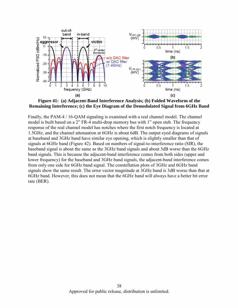
38Approved for public release, distribution is unlimited.
Figure 41: (a) Adjacent-Band Interference Analysis; (b) Folded Waveform of the Remaining Interference; (c) the Eye Diagram of the Demodulated Signal from 6GHz Band
Finally, the PAM-4 / 16-QAM signaling is examined with a real channel model. The channel model is built based on a 2” FR-4 multi-drop memory bus with 1” open stub. The frequency response of the real channel model has notches where the first notch frequency is located at 1.5GHz, and the channel attenuation at 6GHz is about 6dB. The output eyed diagrams of signals at baseband and 3GHz band have similar eye opening, which is slightly smaller than that of signals at 6GHz band (Figure 42). Based on numbers of signal-to-interference ratio (SIR), the baseband signal is about the same as the 3GHz band signals and about 3dB worse than the 6GHz band signals. This is because the adjacent-band interference comes from both sides (upper and lower frequency) for the baseband and 3GHz band signals, the adjacent-band interference comes from only one side for 6GHz band signal. The constellation plots of 3GHz and 6GHz band signals show the same result. The error vector magnitude at 3GHz band is 3dB worse than that at 6GHz band. However, this does not mean that the 6GHz band will always have a better bit error rate (BER).

39Approved for public release, distribution is unlimited.
Figure 42: Output Eye Diagram of the PAM-4 / 16-QAM Tri-Band Signaling and Constellation of 3GHz and 6GHz Bands
Phase noise is another key factor in determining the BER. To sustain a certain BER, the phase noise requirement of 6GHz band is more stringent than that of 3GHz band. Therefore, it is possible for the 6GHz band to have a worse BER even with less interference. To determine the requirement, we look at the clock distribution of memory interface. As the clock of memory circuits is usually provided by memory controllers, a reference clock signal can be transmitted along with data signals on the memory bus. In that case, some of the phase noise can be canceled or reduced. Figure 43 shows one example that explains this phenomenon.
Figure 43: Phase Noise Shaping of Synchronous Signaling and its Effect on Carrier Jitter

40Approved for public release, distribution is unlimited.
Assume the clock and data signals have different delays from the transmitting to receiving end and the difference is d. The effective phase noise ( n(t)) at the output of low-pass filter will be
n(t - d) - n(t), where n(t) is the carrier jitter at the transmitting end. When dis zero, which means the clock and data signals share exactly the same delay, the effective phase noise is zero. When d is infinitely large, which mean n(t - d) and n(t) are two identical but independent random processes, the effective phase noise is then a random process that resembles 1.4× n(t). With a finite but non-zero d, phase noise at different frequency will respond differently. Phase noise at frequencies of 1/ d and its multiples is perfectly cancelled and phase noise at frequencies of 1/2 d and its odd multiples is doubled in magnitude. Therefore, this phase noise shaping effect responds differently with different phase noise spectrum. If the phase noise is white or very broadband, the integrated jitter will remain unchanged. If the phase noise is concentrated at low frequencies, the integrated jitter will greatly reduce. In most cases, the reference clock is generated with PLL and the phase noise spectrum looks like a 1st-order low-pass response, which is flat within the loop bandwidth and decreasing at a rate of -20dB/dec beyond the loop bandwidth, where the loop bandwidth is usually around 10MHz. Some phase noise spectrums can have peaking or damping around the loop bandwidth frequency, depending on the percentage of phase noise contribution from the oscillator, but we focus on only the general case to simplify the derivation. Multiplying the squares of the phase noise spectrum and shaping frequency response, and then integrating in frequency domain, the square root of the result indicates the standard deviation of the effective integrated jitter( ). On a 2” memory bus, the maximum delay difference is about 0.7ns when the data and clock signals are transmitted in the opposite directions. In the worst case, the loop bandwidth is about 1/140 d and the effective jitter reduces by 71% compared to the integrated jitter without shaping ( ). Adding 3rd-order low-pass filtering with 3dB bandwidth of 700MHz to the frequency response of phase noise shaping, the effective jitter reduces even more ( = /4).
Knowing the exact reduction ratio of the effective integrated jitter, we can calculate the BER. As phase noise shifts the in-phase and quadrature signals by cos n(t) and sin n(t), respectively, the corresponding signal dot rotates on the I/Q constellation plot (Figure 44). Error bits occur when the dot rotates out of the decision boundary, which gives us an allowance of phase error in degree. With the phase error allowance, we can find the BER by comparing the error allowance and standard deviation of carrier jitter. Assume the distribution of carrier jitter is Gaussian. If the ratio of the error allowance to standard deviation is larger than 7, the expected BER is lower than 10-12. While transmitting different signals, the corresponding dot locations and error allowances will be different. Also adjacent-band interference and carrier phase error could shift the dots and shrink the error allowances. Including all these factors, the BER equation is shown in Figure 44,
is the carr v is the adjacent-band interference in amplitude. The phase interpolation used in this work provides maximum step size of 1.2ps, which is ±1.3°of carrier phase error at 6GHz and the 30dB error vector magnitude (EVM) of 6GHz band is equivalent to 3.1%. With these two numbers, we find that the jitter requirement for BER < 10-12
is about 2° or 3.8psrms at 6GHz if counting the phase noise shaping effect. The integrated jitter requirement of 3.8psrms or equivalently 53.2psp-p for BER < 10-12 is comparable to that of 10Gb/s NRZ signaling.

41Approved for public release, distribution is unlimited.
Figure 44: Bit Error Rate and Jitter Requirement Calculation of 16-QAM
There are a couple of other requirements that need to be specified. Previously, we mentioned that the second passband is available because differential signaling is used to suppress the 2nd-order harmonic from the first passband. Ideally with 50% duty cycle of the 3GHz carriers, the 2nd-order harmonic will be completely eliminated. In reality, the duty cycle could deviate from 50% and induces additional adjacent-band interference from the 2nd-order harmonic. Therefore, the carrier duty cycle error needs to be within ±1% to have the additional interference 30dB smaller than the desired signal. Another requirement is theco-band interference, which is also known as crosstalk. Again, we wish the interference to be 30dB less than the desired signal; we need the crosstalk at 6GHz to be less than -30dB. For memory interface, far-end crosstalk (FEXT) is of more concern than near-end crosstalk (NEXT) because data signals are always transmitting in the same direction during either the reading or writing stage. On a 2” FR-4 memory bus with line pitch of 6mil, the FEXT is below -30dB at 6GHz, which meets our requirement.
4.2.3 Circuit Design of Tri-Band PAM-4 / 16-QAM Transmitter
The transmitter of tri-band PAM-4 / 16-QAM signaling is composed of five identical modulation paths, each with one 2-bit DAC, one mixer, and one output buffer (Figure 45).
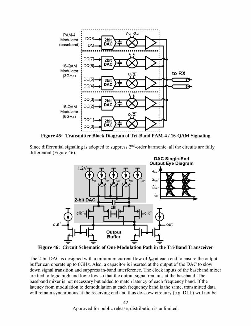
42Approved for public release, distribution is unlimited.
Figure 45: Transmitter Block Diagram of Tri-Band PAM-4 / 16-QAM Signaling
Since differential signaling is adopted to suppress 2nd-order harmonic, all the circuits are fully differential (Figure 46).
Figure 46: Circuit Schematic of One Modulation Path in the Tri-Band Transceiver
The 2-bit DAC is designed with a minimum current flow of Iref at each end to ensure the output buffer can operate up to 6GHz. Also, a capacitor is inserted at the output of the DAC to slow down signal transition and suppress in-band interference. The clock inputs of the baseband mixer are tied to logic high and logic low so that the output signal remains at the baseband. The baseband mixer is not necessary but added to match latency of each frequency band. If the latency from modulation to demodulation at each frequency band is the same, transmitted data will remain synchronous at the receiving end and thus de-skew circuitry (e.g. DLL) will not be

43Approved for public release, distribution is unlimited.
required for data recovery. For common channel medium used for memory interface (e.g. FR-4,silicon interposer, TSV, InFO), group delay variance is negligible ( 0.1UI) over the threefrequency bands. Therefore, as long as the latency of modulation and demodulation paths matches, the total latency matches. The clock inputs of the other four mixers are separately connected to four carriers generated from the dual-band carrier generator, which will be discussed in the next section. Finally, the output buffer is simply a current mirror with feedforward bias circuit to subtract the common mode and output only the differential mode. For output impedance matching, an optional matching circuit is inserted, which can be turned on and off according to channel condition. For short-reach application with less stringent impedance matching requirement, the circuit can be turned off to reduce power consumption and improve energy efficiency.
4.2.4 Circuit Design of Dual-Band Carrier Generator
The carrier generator, which is shared among four lanes of the tri-band transceiver, provides the in-phase and quadrature carriers at 3GHz and 6GHz. In order to maintain orthogonality after demodulation, the carriers at the receiving end must stay synchronized with the propagating signal, and thus the carrier generator must be able to adjust the carrier delay. The carrier generator is composed of one 12GHz clock buffer, two dividers (÷2), and four phase interpolators (Figure 47).
Figure 47: Block Diagram of the Dual-Band I/Q Carrier Generator
The clock buffer first amplifies a 12GHz clock from either a phase-locked loop or an off-chip clock sources. The 12GHz clock buffer is then followed by the first divider. The first divide-by-2circuit generates both in-phase and quadrature carriers phase at 6GHz which are then buffered to drive the transmitter mixer. To drive the receiver mixer, the carriers are delayed to synchronize with the received signal. The carrier delay is imposed by the phase interpolator and thus two independent phase interpolator are used for the two in-phase and quadrature carriers. One of the two outputs of the first divider is applied to the input of another divider that generates the in-phase and quadrature carriers at 3GHz. Similarly to the 6GHz carriers, the 3GHz carriers are buffered to drive the transmitter mixers and phase interpolated by another pair of phase interpolators to drives the receiver mixers. The carrier generator adopts CML topology, whichprovides better supply noise rejection, better duty cycle accuracy and less I/Q mismatches compared to CMOS logic topology. The CML topology also can provide appropriate dc bias for mixers at both the transmitting and receiving ends. The divider has two CML D latches in a

44Approved for public release, distribution is unlimited.
negative feedback loop. Ideally, that will provide 50% duty cycle carrier and zero I/Q mismatch. Layout and random mismatches lead to duty cycle error and I/Q mismatch so the circuits need to be laid out carefully to reduce systematic mismatches. The random mismatch caused by local variation is well-controlled by device sizing.
The adjustable delay required for carriers at the receiving end is realized by interpolating the in-phase and quadrature carriers with a tail-current summation phase interpolator. The phase interpolator produces a weighted sum of two input carriers with quadrature phase difference in this case. The phase interpolator interpolates between the in-phase and quadrature carriers and provides a clock phase in between. A total of 90 degree phase rotation can be achieved which is equivalent to 41.6ps delay range for 6GHz carriers and 83.2ps delay range for 3GHz carriers. By controlling the tail current weight, the output clock phase and delay can be controlled. In this design, forty identical tail current units and 6 control pins are used so that a resolution of 1.2ps for 6GHz and a resolution of 2.4ps for 3GHz can be achieved. In-phase and quadrature clocks are delayed separately by two identical phase interpolator but with inputs with swapped polarities. In order to improve the linearity of the phase interpolator, the input and output time constant (slew rate) of the phase interpolator needs to be carefully controlled. The time constant should not be too fast for phase mixing quality.
4.2.5 Circuit Design of Tri-Band PAM-4 / 16-QAM Receiver
Similar to the transmitter, we can find five identical demodulation paths in the receiver of tri-band PAM-4 / 16-QAM signaling (Figure 48).
Figure 48: Receiver Block Diagram of Tri-Band PAM-4 / 16-QAM Signaling
Before the demodulation paths, there is an input buffer that includes a 1-to-5 current mirror to distribute the received signal. The input buffer also provides impedance matching for both the transmitter and receiver. Within the input buffer, a gain-reduced regulated cascode structure is

45Approved for public release, distribution is unlimited.
used and its differential input impedance is determined by transconductance difference of the NMOS and PMOS, which is equivalent to (2/gmn–2/gmp) at low frequency (Figure 49).
Figure 49: Circuit Schematic of the Gain-Reused Regulated Cascade Input Buffer
Therefore, with proper sizing of those transistors, the differential input impedance can be as low gmn is
larger than gmp and induce a negative input impedance. This is possible when the bias current andthe transconductances are too small. With a transconductance variation of ±2.5%, negative input impedance is possible when the design values of gmn and gmp are lower than 1/1050 and 1/1000, respectively. Besides the stability problem, a small bias current could also cause impedance mismatch at high frequency. With parasitic capacitance (Cp) at the gate of PMOS, the equation can be modified as (2/gmn– 2/(gmp p)) and thus the input impedance will start increasing beyond a corner frequency. With a larger bias current and hence larger transconductances, the corner frequency can be higher and the impedance matching condition can sustain within a wider frequency range. There is a circuit technique that can help to extend the corner frequency without increasing the bias current. By inserting a small resistor between the gate and drain of PMOS, the effective gmp will reduce at high frequency, which forms an inductance to balance the parasitic capacitance. In this work, the resistor helps to improve the input return loss, S11, by 12dB at 6GHz (Figure 50).
Figure 50: Simulated S11 Frequency Response of the Gain-Reused Regulated Cascade Input Buffer
Note that the inductance and capacitance could resonate and destabilize the input buffer, and thus the variation of the resistor also needs to be well controlled. An additional switch transistor is inserted between the NMOS and the bias current source at each side so that we can turn off the

46Approved for public release, distribution is unlimited.
matching circuit if not used. While turned on, the switch transistors have a small but not zero resistance, so the transconductance difference needs to be smaller in order to maintain
With the 1-to-5 current mirror inside the input buffer, each demodulation path received one copy of the input signal. Then the signal is down-converted with a mixer, reconstructed with a low-pass filter and finally digitized with a 2-bit ADC. Again, all the circuits are fully differential to suppress 2nd-order harmonic (Figure 51) and the baseband mixer is retained for latency matching.
Figure 51: Circuit Schematic of One Demodulation Path in the Tri-Band Transceiver
According to the system analysis performed in Section 2.2, the low-pass filter is built as 3rd-order structure with 30dB rejection at 3GHz offset. To maximize the output eye diagram, the transfer function of the low-pass filter is designed as Bessel function with linear phase and maximally flat group delay, which has no ringing or peaking in step response. For a Bessel function with 30dB rejection at 3GHz offset, the 3dB bandwidth is about 700MHz. To implement such a high bandwidth filter, Gm-C architecture is adopted for its low power consumption while compromising on linearity (Figure 52).
Figure 52: Block Diagram of the 3rd-Order Bessel Gm-C Low-Pass Filter
Also, the three Gm stages in the middle share one bias current source in order to further reduce power consumption. Finally, the 2-bit ADC is composed of three parallel comparators. Inside each comparator, the first two stages are used as a cherry hopper preamplifier. Between the first and the second stage, a reference current is injected from an auxiliary DAC which is used for threshold adjustment and offset calibration. After amplification, two cascaded set-reset (SR)latches convert the differential analog signal into a single-ended digital bit stream. With the two cascaded SR latches, the output state change only when the differential input signal crosses threshold at both sides, which avoid change of duty cycle due to common-mode mismatch

47Approved for public release, distribution is unlimited.
between analog and digital stages. Then, the three latch output bits are mapped back to two bits with a 2-bit decoder.
4.2.6 Circuit Design of 4-Lane Transceiver with Built-In Self-Testing (BIST)
Combining four transmitters, four receivers, and one carrier generator, we obtain a 4-lanetransceiver that achieves a total data rate of 40Gb/s (Figure 53).
Figure 53: Illustration of the Transceiver Testing Environment with Built-In Self-Tester
During measurement, the 4-lane transceiver requires a testing pattern of 40 bits with symbol rate of 1GBaud, which is very difficult to generate from regular testing instruments or general-purpose field-programmable gate array (FPGA) boards. Therefore, we choose to implement a BIST machine integrated with the 4-lane transceiver. The BIST is composed of a 32-bit pseudo-random binary sequence (PRBS) generator and a 32-bit error detector. PRBS generators are usually implemented with linear-feedback shift registers (LFSR). In order to verify BER less than 10-12, the LFSR’s repeat cycle needs to be larger than 1012, which is close to 240, which means the length of the LFSR needs to be at least 40. Also, for each of the 32 independent PRBSs, we need one primitive feedback polynomial but we cannot find 32 primitive feedback polynomials with a length of 40, which means some of the 32 LFSRs need to have lengths longer than 40. Therefore, it is not efficient in terms of power and area to implement a 32-bit PRBS generator with conventional LFSR. In this work, the 32-bit PRBS generator is composed of only two reservedly combined LFSRs each with lengths of 32 and 33, respectively (Figure 54).

48Approved for public release, distribution is unlimited.
Figure 54: 32-bit PRBS Generator Implemented with Reversely Combined Linear Feedback Shift Registers (LFSRs)
Reverse combination and length difference are two keys to efficient multi-bit PRBS implementation. If the two LFSR are combined in the same direction, then the output PRBSs will not be independent but identical with time shift. If the two LFSR have the same length of 40, the repeat cycle will be (240 – 1), which is enough for BER < 10-12 but much smaller than (232-1) × (233-1) when having lengths of 32 and 33. Two LFSR with different lengths of 32 and 33 are apparently more area efficient than those with the same length of 40.
Similar to the 32-bit PRBS generators, the 32-bit error detector also has its own design difficulty. Since DDR3 memory interface, a retiming technique using DLL is adopted to synchronize multiple bits of received data. Physical channel difference due to PCB routing and PVT condition induces delay variation between data and clock signals. Before DDR3, people simply bundle every 8 bits of data signal (8 DQs) and assign one clock signal (1 DQS) so that the delay variation within each bundle can be tolerable. However, since DDR3 achieves a data rate up to 2.133GHz, even the delay variation within each bundle could cause error bit during data recovery. As a result, DLL is used to adjust the delay of and synchronize every DQ within a bundle so that the assigned DQS can correctly recover received data. Nevertheless, the introduction DLL creates circuit overhead and limits the reduction of power and area efficiency. In this work, we utilize a characteristic of multi-band signaling to avoid the necessity of DLL. As mentioned before, the delay variation within the 10 modulated bit streams of each lane is negligible because they share the same physical channel. Therefore, if we simply assign one of the 10 bit streams to be the DQS, then we can directly use the demodulated DQS as the clock for data recovery. Here we modulate the DQS at baseband together with the data mask (DM), a low-speed signal bundled with 8 DQs and 1 DQS in DDR series memory. However, since DQS is a clock signal and its harmonics are more concentrated in spectrum compared to those of random data, the adjacent-band interference is more severe in time domain (Figure 55).

49Approved for public release, distribution is unlimited.
Figure 55: Illustration of the Transceiver Testing Environment with Built-in Self-Testing
As a result, the baseband signal is slightly turned down in order to reduce interference to 3GHz signal. Finally, the 32-bit error detector consists of 4 sets of 8-bit error detector and each is triggered with its assigned DQS. Also, each 8-bit error detector required one 32-bit PRBS generator triggered by the DQS so that we can compare the received data with the PRBS output. The comparison result can be accessed by personal computer or notebook via an integrated UART interface. The UART interface can operate at speeds up to 3MBaud and it has extra register file that is assigned to control pins for the transmitter, receiver and carrier generator.
4.3 Development of MRFI Serial Links
As a result of the ever increasing connectivity requirements for communication, computing, and consumer system applications, the data traffic for I/O bandwidth is increasing with time. The chip pin count, however, is still limited by the packaging. Therefore, high speed serial links with tens of gigabits are in great demands: data rate per pin has approximately doubled every four years for a variety of I/O standards [1].
The most widely adopted serial links are NRZ time-domain-multiplexing (TDM) links. Figure 56shows the architecture of a conventional baseband transceiver that typically includes a serializer and an output driver at the transmitter and a CTLE, a decision feedback equalizer, a deserializer and a clock data recovery circuit at the receiver. Baseband-only TDM links multiplex data in time-domain.

50Approved for public release, distribution is unlimited.
Figure 56: System Architecture of a Typical NRZ Serial Link
As data rates of serial links increases, however, great challenges arise: 1) channel and packageimpairments, and 2) non-linear power-speed trade-offs. First, signal loss, reflections, and cross-talk are more pronounced at higher frequencies. Therefore, high-speed NRZ links suffer greatly from inter-symbol interferences (ISI). Better packaging, connector, via technologies, and material can be used to improve the channel characteristics and reduce loss and reflections, but itcan be costly and may not be suitable for every scenario, e.g. existing data centers. Equalization circuits can be implemented to alleviate ISI but it can be painful especially for MDBs and high-loss channels. For example, in order to equalize 30dB loss at Nyquist rate, a CTLE and a DFE of 10-20 taps along with a FFE with at least 3-5 taps [2, 3, 4]. The second challenge is the tough timing margin for high speed serial links. As the symbol period reduces, timing margins for both equalization circuits as well as clock data recovery circuits are reduced proportionally. The stringent timing margin leads to more circuit complexity such as unrolled DFE. In order to deal with these issues, energy efficiency of high-speed NRZ serial links are limited.
In order to live with channel loss and to improve energy efficiency for ultra-high-speed serial links, more efficient use of the available link bandwidth is needed. Multi-level signaling schemes, for example, PAM-4 are gaining more popularity for ultra-high-speed serial links. Multi-level signaling scheme consumes less bandwidth than NRZ signal, which makes multi-level signaling more attractive for ultra-high-speed serial links. For example, the bandwidth of PAM-4 data stream is one half of the bandwidth of NRZ data stream under the same data rate. Nevertheless, due to reduced signal power, multi-level signaling is more sensitive to ISI and noise. Even worse, it would also increase the complexity for traditional equalization and clock recovery circuit due to its multi-level nature. The most recently published 4-PAM transceivers are implemented with ultra-high-speed moderate-resolution ADCs, which took advantage of modern CMOS technology [5]. However, the ultra-high-speed ADCs are still very challenging and power-hungry.
An alternate way to overcome the channel loss and improve link bandwidth utilization is multi-band signaling. The conceptual multi-band serial link is shown in Figure 60.

51Approved for public release, distribution is unlimited.
Figure 57: Conceptual Multi-Band Serial Links
Recent studies show that multi-band signaling can alleviate channel non-ideality with better energy-efficiency [6, 7, and 8]. First, because of the characteristics of the wireline channel and the up-conversion and down-conversion operation, multi-band signaling using direct-conversion architecture can effectively self-equalize the channel loss [7], greatly reducing ISI. This is illustrated in Figure 58. Second, for multi-band links, each sub-band can have much smaller bandwidth so that the timing margin of the circuits can be greatly relaxed. Last, multi-band links are very efficient to deal with channel notches [6]. The previous works [6, 7, and 8] accomplished by our Lab used low-order modulation scheme (QPSK/16-QAM) and the aggregated data rates has reached up to 10 Gb/s with an energy-efficiency of around 1pJ/bit.
Figure 58: Self-Equalization of Direct-Conversion Multi-Band Links [7]
In order to further increase the data rates and improve spectral density, we designed a receiver front-end which is capable to demodulate high order modulation scheme to increase I/O bandwidth to 16Gb/s. The receiver front-end also includes a baseband path sharing the same physical channel for clock recovery and a programmable input buffer for better impedance matching to provide constant group delay. An Inter-band interference cancellation algorithm is also investigated to compensate non-idealities of low-pass filters and improve energy-efficiency of the link.
4.3.1 TX Design for MRFI Serial Links
We have successfully designed and implemented a cognitive transmitter with multi-band signaling and channel learning mechanism in TSMC 28nm High Performance Computing (HPC)technology (Figure 59).
N:1FDM
Serializer
1:NFDM
De-Serializer
N-wayParallel
Data@ 1/(nTs)
::
::
N-wayParallel
Data@ 1/(nTs)Multi-band
Freq.-domainRF signal
f2f1I
Freq.Q
B B

52Approved for public release, distribution is unlimited.
Figure 59: System Architecture of Cognitive Transmitter with Multi-Band Signaling and Channel Learning Mechanism
The cognitive tri-band transmitter with forwarded clock uses base band, 3-GHz RF band, and 6-GHz RF band. The transmitter features learning an arbitrary channel response by sending a sweep of continuous wave, detecting power level, and accordingly adapting the modulation scheme, data bandwidth and carrier frequency. The modulation scheme ranges from NRZ/QPSK to PAM-16/256-QAM. The highly re-configurable transmitter is capable of dealing with low-cost serial link cables / connectors or multi-drop buses with deep and narrow notches in frequency domain (e.g. 40dB loss at notches). The adaptive multi-band scheme mitigates equalization requirement and enhances the energy efficiency by avoiding frequency notches and utilizing the maximum available signal-to-noise ratio and channel bandwidth. The implemented transmitter consumes 14.7mW power and occupies 0.016mm2 in 28nm CMOS. It achieves a maximum data rate of 16-Gb/s per differential pair and the most energy-efficient figure of merit (FoM)* of 20.4 μW/Gb/s/dB considering channel condition. (*The physical meaning of FoM is the power consumption of transmitting per Gb/s data and overcoming per dB worst-case channel loss within Nyquist frequency).
The data rate of peripheral serial I/O for PCs and mobile computing platforms continue to scale to meet high-bandwidth applications including high-resolution displays/camera sensors and large-capacity external storage [1]. Recent publications demonstrated a multi-band signaling architecture to meet such stringent requirements in cost and energy efficiency [2-4]. Typical low-cost cables/connectors and MDB impose notches and non-linearity in the frequency domain resulting from the resonance effect. The multi-band signaling takes advantage of such impairments by transferring data via multiple modulated-carriers where there is no such non-ideality. The previous work, however, works only with one specific cable/connector configuration, because not only is the carrier frequency fixed, but also there is no mechanism to gain knowledge on the channel conditions. In order to provide a universal solution capable of handling all different channels, we propose a cognitive tri-band forwarded-clock serial link TX with a frequency response learning algorithm. The TX senses the channel condition by first sending a single tone from 50 MHz to 10 GHz. Then the detector measures the received power
Delay matching
Cognitive Tri-Band TX
Low-speed Single-ended
Back Channel
CognitiveController
Carrier Freq.ModulationData Rate
DC
4-bit DAC
4-bit DAC
÷ 290°
0°4-bit DAC
4-bit DAC
÷ 490°
0°4-bit DAC
Tri-Band Signal
Mod.Mappping
EXTCarrier
OSC
Two RF Bands
Channel Response
Detection @RX side
Power Detector
ADC
Baseband
Base-line tri-band TXCognitive blocks

53Approved for public release, distribution is unlimited.
on the other side of channel and feeds it back to the TX. With this information, the TX cognitive controller determines the carrier frequencies, modulation scheme, and bandwidth based on the system BER and data rate requirement.
4.3.2 Channel Responses with Frequency Notches
The common scenario of low-cost peripheral I/Os and its channel insertion loss is depicted in Figure 60(a). When considering a cable-only case, the dielectric and conduction loss would exhibit a simple low-pass characteristic. In Figure 60(b), the complete channel including packages, solder balls, wire-bonds, vias, traces and connectors suffers from higher loss at certain frequencies. This leads to the higher dispersion and distortion of signal. The phenomenon is more pronounced in low-cost packaging, PCB, cable and connector technologies. Another example of having such non-idealities is the case of MDB. As shown in Figure 60(c), there could be multiple notches with more than 40dB loss. The deep and narrow of notches require complicated equalization or sensitive compensation technique, which are not energy and costefficient solutions.
Figure 60: (a) Common Periphery Serial Link; (b) Cable-Only and Complete Channel Insertion Loss; (c) With and Without MDB Insertion Loss
Figure 61 shows the memory controller with two DIMMs per channel. Figure 62 shows the time-domain single-bit response.

54Approved for public release, distribution is unlimited.
Figure 61: Memory Controller with Two DIMMS per Channel
Figure 62: Time-Domain Single-Bit Response
Figure 63: Conceptual Comparison of Baseband TX and Multi-Band TX
In order to make the merits of multi-band signaling more intuitive to understand, we conducted several simulations to compare multi-band and conventional base-band. Assuming the data rate requirement is 15Gb/s, multi-drop memory interface channel with frequency notches is used. Figure 64 (upper figure) shows the spectrum of base-band signal - the energy is distributed uniformly. When the signal passes through the multi-drop memory interface channel, severe reflections occur and strong inter-symbol interference makes the data eye close completely. Complicated and power-hungry equalization is necessary to open the data eye.
Package Pins
Vertical Connector
DIMM 0 DIMM 1Controller
Ts Ts Ts Ts
Time-domain Baseband Signal
Frequency-domain Multi-band Signal
f2f1
B
f2fff1f1
f2
IQ Mixer

55Approved for public release, distribution is unlimited.
Figure 64: Baseband TX vs Multi-Band TX on Multi-Drop Memory Interface Channel
The lower part of Figure 64 shows the spectrum of multi-band signal. The energy distribution ispurposely shaped based on the channel profile. After tri-band demodulator, the data eyes are clearly opened, at the same data rate assumption, channel condition, and without equalization. Another point to emphasize is that the time scale is different. For base band, the time is around 100ps while for tri-band, the time axis is 2ns. By utilizing multi-band signaling, each data stream actually runs at a lower speed which greatly relaxes the clock-data recovery system design.
4.3.3 Phase Calibration and Phase Recovery for Serial Interface
With 16-QAM modulation as an example, phase offset leads the constellation rotation, with 15 degree rotation (Figure 69). The data eye is completely closed and BER is very poor. Phase recovery or calibration is required to achieve reasonable eye quality and BER. Wireless and serial interface phase recovery requirements are very different. For a wireless system, phase recovery should be real-time and track fast changing channel characteristics, which is handled by baseband DSP. For a serial interface system, simple calibration should work as channel condition is almost fixed; there is no need to dynamically track.
---------------------------------------------------------------------------------------------------------0 3 6 9 12 15
frequency (GHz)
15:1 NRZSerializer(15Gb/s)
DQ[0]
DQ[14]
15:1 NRZDeserializer
(15Gb/s)
0 2 4 6 8 10frequency (GHz)
DQ[0]
DQ[14]
0 67 133time (ps)
33 100
Package Pins
Vertical Connector
DIMM 0 DIMM 1Controller
Tri-Band Modulator(15Gb/s)
DQ[0]
DQ[14]
Tri-Band Demodulator
(15Gb/s)
0 2 4 6 8 10frequency (GHz)
0 2 4 6 8 10frequency (GHz)
DQ[0]
DQ[14]
0 1 2time (ns)
0.5 1.5 0 1 2time (ns)
0.5 1.5
Base-Band
3GHz-Band6GHz-Band

56Approved for public release, distribution is unlimited.
Figure 65: Phase Offset Impact on Data Eye Quality
If we plan to do phase calibration by DSP (similar to the wireless system), we will end up with high resolution ADC, which is out of the power budget of serial interface. ADC resolution requirement for data decision and phase calibration are very different. Take 16-QAM as an example - only 2-bit ADC is required for data decision, however phase calibration requires 8-bit ADC. Table 3 shows the different specification of ADC effective number of bits (ENOB); 256-QAM needs 12-bit ADC ENOB running at multi-GHz. The state-of-the-art ADC consumes more than 5W power, which cannot be tolerated by the power budget of serial interface.
Table 3. ADC Resolution Specs of Phase Calibration for Different Modulation Schemes
With our proposed phase calibration scheme, before data transfer, the lower Q-path is turned off, and a constant input at upper I-path is set. The I- - -path output at RX side is- - -delayed; this is an unknown but fixed value for serial interface, depending on channel length, substrate dielectric and channel dimensions.
-path output is 1 and Q-path output is 0. RX will save this phase code for data transfer; this phase code actually rotates the constellation back. In the proposed approach, only 1-bit ADC is needed because we only need to detect zero across point, which give us optimal phase code. Thus high-resolution ADC and complicated baseband DSP are avoided, as shown in Figure 66.

57Approved for public release, distribution is unlimited.
Furthermore, even with IQ imbalance, phase calibration still works because phase offset error is decoupled from IQ mismatch. IQ imbalance only changes the slope around zero crossing point, but does not change the location of zero crossing point. As long as we have sensitive comparator in ADC front-end, we are able to get reasonable accurate phase code.
Figure 66: Proposed Phase Calibration Scheme with One-Bit ADC
4.3.4 Link Budget Calculation and Clock Forwarded Architecture
Figure 67 shows how the cognitive controller calculates link budget based on the BER requirement. Here we show the link budget calculated based on 10-12 BER. From transmitter output, channel loss, margin, and then signal to noise ratio (SNR) requirement from different modulation, receiver noise figure, integration bandwidth and thermal noise floor. The link budget changes when different channel conditions and different modulation schemes are chosen.
Figure 67: Link Budget Calculation
f0
1-bitDAC
1-bitDAC
1-bitADC
1-bitADC
‘1’
OFF
0°+90°
f00°
90°+sin
-cos
t
17dB 24dB 30dB36dB
TX output powerChannel Loss & Margin
Bandwidth
RX Noise Figure
QAM256 Required SNR
Thermal Noise Floor
-20dBm
-174dBm/Hz
-84dBm
-74dBm
-38dBm
Required SNR @ BER < 10-12 24dB 30dB 36dBBits per Symbol 2 4 6 8
Channel BW 1GHz 1GHz 1GHzData Rate 4Gb/s 6Gb/s 8Gb/s
SNR (dB)
BER

58Approved for public release, distribution is unlimited.
Figure 68 shows the traditional source-synchronized system, which reduces the complexity and power of clock generation and data recovery circuits, at the cost of an extra dedicated physical channel and clock I/O pins serving on clock forwarding purpose. However, for the proposed serial interface, there is a baseband path which can be configured to serve for clock forwarding purposes. In this way, there is extra I/O pin and channel as needed. Everything is embedded into frequency domain by multi-band signaling. Without PLL-based clock and data recovery (CDR),it saves the power and reduces the complexity.
Figure 68: Conventional Source-Synchronized / Forward Clocking Architecture
4.3.5 Circuit Design Cognitive Tri-Band Transmitter Building Blocks
DAC is the current steering structure; there is a capacitor at DAC output to limit DAC bandwidth on purpose in order to address in-band inter-band interference (IBI). Double-balanced mixer and DAC are combined within the same stage for power saving purposes (Figure 69). All designs are fully differential current mode to suppress 2nd order harmonic and other common mode noises. The bias current is digitally tunable based on link budget and energy efficiency optimization. Its value is set by the cognitive controller.
Figure 69: Digital-to-Analog Convertor and Mixer Schematics
TX Chip
TX Data
TransmittedClock
TX PLL
RX Data
RX Chip
Forward-Clock Channel
Received Clock
. . .Vb VbD0 D0b D1 D1b D15 D15bIbias
CLK CLKbCLKb
Mixer
4-bit DAC
Mirror to Summation block I_NI_P

59Approved for public release, distribution is unlimited.
As shown in Figure 70, the summation block consists of five slices, for two RF I and Q bands and baseband. A 100 Ohm termination resistor and a switch are attached in series at the end, which can improve impedance matching if necessary. The block needs to sum all signals from all bands to provide broadband operation up to 7GHz. It also needs to substrate DC current to avoid desensitizing receiver front end. This is the path we copied a portion of DC current from input and subtracted from output.
Figure 70: 10 Five-Slice Summation Block Schematics
Figure 71: Fully Reconfigurable Receiver Front End Schematics
As shown in Figure 71, the receiver front end is a fully reconfigurable design. It provides broadband operation and very large impedance matching coverage from 50 Ohm to 150 Ohm, to cover different channel conditions and to compensate fabrication variations. Gain-reused structure is used to boost the gain and improve sensitivity, while not consuming too much power. Digital-tunable regulated resistor is used to improve high-frequency broadband operation. DC
Baseband
÷4 In-phase÷4 Quadrature
÷2 In-phase÷2 Quadrature
From M
ixer
I_N
0.1x(I_P+I_N)=0.2xIdc
1x10x 10x
1x
DifferentialChannel
Iout_P=I_P-Idc
Iout_N=I_N-Idc
I_P1y
5y 5y
DifferentialChannel
Binary Weighted Slice x2
Binary Weighted Slice x4
Slic
e EN
[2..0
] Gain-reusedRegulatedCascode
Slice Enable & Bias
Slice Enable & Bias
3-bit
3-bit
Binary Weighted Slice x1

60Approved for public release, distribution is unlimited.
bias current is also tunable. In summary, we can use 3-bit slice to enable control and 6-bit tuning for each slice. All this reconfigurable ability allows the proposed serial interface to cover a lot of different channel conditions and maintain high performance and low power even with fabrication variations.
Table 4. MRFI Serial Link Performance Metrics
MRFI Serial Link Performance MetricsTechnology 28nm HPC (TSMC)
Selected Frequency Bands Baseband / 3GHz / 6GHz
Modulation NRZ/QPSK, PAM-4/16-QAM, PAM-8/64-QAM, PAM-16/256-QAM
Aggregated Data Rate 16Gb/s/laneSupply Voltage 1.2V
Target Channel 2” dense FR-4 or multi-drop memory interface channel or low-cost cable channel
Energy Efficiency 3pJ/bitCell Area 0.03mm2/lane*
*ADC area not included.
4.3.6 MRFI Serial Link Receiver Design
The multi-band receiver consists of three demodulation paths: one PAM demodulator via the baseband and two QAM demodulation via the two RF bands. Two RF carrier frequencies are generated from one external clock source and have a fixed frequency relationship of f1=2*f2. These frequencies can be tuned through changing the external clock frequency so that the input spectrum can be adjusted to match different channel responses (e.g. channel notches) to reduce inter-symbol interference. IBI, however, is another major source of interferences for multi-band serial links. While inter-symbol interference results from the limited bandwidth of channel and electrical circuits, inter-band interference are mainly determined by carrier frequency allocation and filter design. As the modulation order gets higher, e.g. 64-QAM/256-QAM, the receiver performance becomes more sensitive to interferences. To analyze the interferences, pulse-response-based analysis is utilized.
In our receiver system, the low-pass filter output is a ‘symbol-wise’ linear time-invariant response due to the choice of our carrier frequencies f1, f2 are integer multiples of symbol rate. This relationship can be proved by the following equations by assuming that carrier frequencies are , where = 1,2,3 … . Each symbol has duration of and can be represented as
s(t) = g(t) ( ) , . (3)

61Approved for public release, distribution is unlimited.
(4)
If a symbol is transmitted at time slot 0, the received waveform can be presented as y (t) = LPF( ) sin(2 f t ) cos(2 f t ) g(t ) ( ),If the symbol is transmitted at time slot K, the received waveform can be presented as
(t) = LPF( ) sin(2 f t ) cos(2 f t ) g t KK K(5)
= LPF( ) sin 2 f t K cos 2 f t K g tK K K(6)
= ( K ) (7)
. Therefore, we can express the low-pass filter output as:
( ) = [ ] ( ) + ( ) ,= 1,2,3,4,5 (8)
[ ] ,( ) , . Inter-symbol interferences are determined by ( ).As a result of the self-equalization effect of direct-conversion and comparatively long symbol period (1ns for 1GHz symbol), ( ) has a duration of less than 2ns in multi-band serial link system. This means that the inter-symbol interferences have negligible effect if we sample the output at the right time. On the other hand, the cross terms ( ), determine inter-band interferences. The carrier frequency allocation and low-pass filter design determines ( ), .Usually, these cross terms are suppressed by makingf1 – f2 much larger than the symbol rate or using high order low-pass filters. However, by taking power and design complexity into consideration, we choose to keep f1-f2 as small as possible and the order of low-pass filter low. An inter-band interference cancellation algorithm is also devised in addition to improve energy-efficiency.

62Approved for public release, distribution is unlimited.
4.3.7 Receiver Clock Recovery and Sample Timing Optimization
In a digital communication system like our multi-band serial link, the output ought to be sampled by an analog-to-digital converter and then decoded into digital bits. In conventional serial links, there are two ways to generate the proper timing for receiver sampling: source-synchronize clocking and phase-lock loop based clock data recovery. In a source-synchronized serial link, the clock is usually forwarded to the receiver using a separate dedicated physical channel and I/O pin. Compared with source-synchronized serial link, phase-lock loop based clock data recovery architecture requires no extra physical channel or pin at the expense of higher energy consumption than that of a source-synchronized serial link.
In our multiband interconnect system, source-synchronizing approach is adopted. However, unlike traditional serial links, the clock is sent simultaneously along the same physical channel with data signals via different frequency bands. Therefore, no extra physical channels or I/O pin is needed. After the clock is recovered by using a low-pass filter to remove data signals carried by RF bands, the clock signal is passed through a programmable delay line where the sampling time is optimized and inter-symbol interferences is minimized. The sampling timing calibration algorithm is proposed in Figure 72.
Figure 72: Embedded Forwarded Clock
Since our concern is inter-symbol interference at this point, we assume that there is no inter-channel interference which is a justifiable assumption since there is no correlation between inter-symbol interference and inter-channel interference; in real application, we can ensure this situation by turning on only one band. Therefore, our received signal can be expressed as:y[n] = [ ] [ ] , where [ ] is the pulse response (9)
Since our system experiences very little ISI, we can consider only 3-4 taps. Therefore, the above equation reduces to: y[n] = [ ] [ ] (10)
= [0] [ ] + [1] [ 1] + [2] [ 2] + [3] [ 3] (11)[0] [ ]is signal and [1] [ 1] + [2] [ 2] + [3] [ 3] is inter-symbol interference.

63Approved for public release, distribution is unlimited.
Assuming that S[n], S[n-1],S[n-2],S[n-3] are uncorrelated symbols and have the same mean and variance, signal to interference ratio can be calculated as
= 20 = 20 [0][1] + [2] + [3] (12)
Figure 73 shows the relationship between sampling time and signal-to-interference ratio (SIR).In conclusion, our task to determine the optimal sampling point can be formulated as the point where we can find the largest SIR as Figure 74 shows.
Figure 73: SIR vs Sampling Timing
Figure 74: Sampling Timing Calibration Circuit Block Diagram and Flow Chart

64Approved for public release, distribution is unlimited.
4.3.8 Inter-band Interference and the Cancellation Algorithm
In our multi-band receiver, one of the challenges to improve spectral efficiency is to reduce inter-channel interference. As Figure 75 shows, inter-band interference consists of two parts – intra-band interference which is due to the spectral overlap at transmitter and inter-band interference due to finite roll-off factor of filter. Usually, intra-band interference can be suppressed by pulse-shaping at transmitter and inter-band interference is mostly suppressed by low-pass filter. Pulse-shaping at transmitter can be implemented by a high-speed high-resolution digital-to-analog converter. High-order low-pass filter is needed for high order modulations like 64-QAM/256-QAM. However, both can be power hungry given the operating speed of the circuit. What is more, the bandwidth of low-pass filter varies greatly because of the process, voltage and temperature variations. In order to deal with inter-band interference more efficiently, an interference cancellation algorithm is proposed here.
Figure 75: Inter-band Interferences in Frequency Domain
Based on our previous analysis, when received signals are sampled every T seconds, the low-pass filter output can be simplified into the following equation:
( ) = [ ] ( ) + [ ],= 1,2,3,4,5,6 (23)
This can be reduced to a matrix format,[n] = [ ] [ ]+ [ ] (34)

65Approved for public release, distribution is unlimited.
As proved by our previous study, multi-band links self-equalize channel loss and experience negligible ISI. Also, the time skew of symbols from different sub-channels are negligible. Therefore, we can optimize our sampling timing so that received signal is only determined by symbols at the same time slot. The above equation reduces to= + (44)
If we can determine , we will be able to estimate the transmitted symbol. In order to determine, we can first use training sequence. The whole process can be summarized as Figure 76.
Before the data transmission begins, we first use training sequence to optimize the sampling time. After the sampling is optimized, we ensure that inter-symbol interference is minimized and reduced to a negligible level. After that, we begin to estimate the coefficient matrix . Since the noise level is low (BER < 10-12), we can use a least-square estimator, which gives us= ( ) (15)
where is our training sequence. Therefore, our received symbol is = + (16)
Figure 76: System Operation Flow
Based on the proposed inter-band interference cancellation algorithm, system simulations are performed with 64-QAM modulation. Figure 77 and Figure 78 show the simulation results with the whole system using 6bit ADC. Before any cancellation scheme, the eye-diagram is closed due to IBI. However, with inter-band interference cancellation, data is successfully restored in physical level simulations with error vector magnitude (EVM) of -32dB by using a 6bit ADC.

66Approved for public release, distribution is unlimited.
Figure 77: Constellation and Eye Diagram With and Without Inter-Band Interference Cancellation
Figure 78: Transient Response With and Without Inter-Band Interference Cancellation

67Approved for public release, distribution is unlimited.
4.3.9 Circuit Design of Multi-Band RF Receiver Analog Front-End
Figure 79 shows the receiver input buffer schematic. The input buffer provides broadband impedance matching for the receiver and redistributes the receiver input current to five mixers using a 1 to 5 current mirror.
Figure 79: Programmable Receiver Input Buffer Schematic
Gain-reduced regulated cascode structure provides feedback and reduces the input impedance,which is more energy-efficient than that of conventional common-gate input buffer. Resistors provide active peaking for the diode connected PMOS and it improves the bandwidth of the circuit. The input impedance of the circuit is given by2 2 . In order to coverdifferent matching requirements and to compensate fabrication variations, we designed programmable bias current to change the input impedance by varying and . We also include slice selection to increase the coverage from 50 Ohms to 150 Ohms. Furthermore, the resistors are also programmable to provide desired bandwidth.
DifferentialChannel
Binary Weighted Slice x2
Binary Weighted Slice x4
Slic
e EN
[2..0
] Gain-reusedRegulatedCascode
Slice Enable & Bias
Slice Enable & Bias
3-bit
3-bit
Binary Weighted Slice x1

68Approved for public release, distribution is unlimited.
Figure 80: Simulated Input Impedance for Programmable Receiver Input Buffer
Figure 81 shows the receiver mixer and low-pass filter schematics. The mixer takes input current from input buffer and down-converts the input current signal and passes it onto the low-pass filter to recover the transmitted signal.
Figure 81: Mixer and Low-Pass Filter Schematics
Fifth-order linear-phase low-pass filters are adopted here to provide sufficient suppression on high-frequency interferences and meanwhile maintain relatively constant group delay to minimize ISI. The fifth-order linear-phase low-pass filter consists of three stages: one simple RC stage to provide one single pole and two bi-quads to provide two pairs of complex poles. Since the bandwidth of the low-pass filter should be around 800 MHz, Gm-C architecture is adopted here to improve energy-efficiency. In order to improve linearity for high-order modulation, linearized transconductance cell using local feedback is adopted here, as shown in Figure 82.
Frequency (GHz)
RX In
put I
mpe
danc
e (O
hm)

69Approved for public release, distribution is unlimited.
Figure 82: Linearized Transconductance (Gm) Cell for Low-Pass Filter
4.4 Receiver Front-End Die Photo and Post-Layout Simulation
The receiver front-end circuit, including input buffer, mixers and low-pass filters, are implemented in TSMCN28 HPC technology and is under assembly for testing. Figure 83 shows the test chip die photo and receiver front-end layout.
Figure 83: Die Photo and Layout of Receiver Front-End

70Approved for public release, distribution is unlimited.
The post-layout simulation demonstrates QPSK, 16-QAM, 64-QAM and 256-QAM modulation with receiver front-end. Figure 84 shows time-domain eye-diagram and I/Q constellation. Without any receiver equalization and PLL-based CDR, the proposed receiver front-end should achieve 16 Gb/s.
Figure 84: Eye Diagram and Constellation of Post Layout Simulation
4.5 Benchmarking with State-of-the-Art
In summary, a tri-band interconnect receiver is designed for serial link applications, which is able to demodulate PAM-2, 4, 8, 16/QPSK, 16, 64, 256-QAM signals. It is designed and simulated at the physical level to achieve a maximum of 16Gb data rate with excellent energy efficiency of 3pJ/bit.
The receiver is capable of delineating highly modulated signals up to 256QAM over low-cost serial link cables/connectors or multi-drop buses with deep and narrow notches in frequency spectrum. The designed receiver consumes 48mW using TSMC 28nm HPC CMOS. Compared with state-of-art high-speed serial link receiver, it achieves about twice better energy-efficiency.

71Approved for public release, distribution is unlimited.
Table 5. Benchmarking with State-of-the-Art
Metric [10] VLSI 15 [9] ISSCC 15 [11]ISSCC 16 This Work
Technology 32nm 65nm 32nm 28nm
Data Rate/Lane 7Gb/s 10Gb/s 25Gb/s 16Gb/s
SignalingScheme
BasebandNRZ
BasebandNRZ
Baseband NRZ
Tri-band/QPSK, 16, 64, 256-QAM
Clocking Forwarded Clockwith Extra Channel
-- Embedded Clock
Forwarded Clockwithout Extra
ChannelRx Power 41.3mW 87-89mW 453mW 48mW
Rx Efficiency 5.9pJ/bit 8.7-8.9pJ/bit 17.7pJ/bit 3pJ/bit

72Approved for public release, distribution is unlimited.
5. RESULTS AND DISCUSSIONS
5.1 Phase-I Test Results and Benchmarking with State-of-the-Art
As elaborated in Section 3.1, we have devised a new FDM architecture that can offer simultaneous and orthogonal communication channels in the frequency domain to link high speed data comparable to that of DDR but with self-equalization and zero skew between DQS and DQ signals. For the FDM memory interface, we implemented a multi-band QPSK transceiver which could operate over five frequency bands each at f1 = 1.6 GHz, f2 = 2.4 GHz, f3= 3.2 GHz, f4 = 4 GHz, and f5 = 5.2 GHz, respectively (Figure 85). With up-to-400-Mb/s data on each channel, the transceiver can achieve a total bandwidth of 4 Gb/s while it consumes only 5.4
2.
1.6G
Power spectral density
DQS/DMDQ7/DQ3
DQ6/DQ2
DQ5/DQ1
DQ4/DQ0
2.4G 3.2G 4.0G 5.2G
Figure 85: Channel Spectrum of the FDM Memory Interface with Five-Band QPSK Modulation
In the MRFI memory interface, each frequency band can carry multiple bits of data depending on the modulation scheme. In the case of QPSK modulation, two bits of data are modulated by two orthogonal carrier, I and Q, at the same frequency. With each carrier, the up-converted signal has two sub-bands, the upper and lower sideband, which are identical but mirrored over frequency to each other (Figure 86).
=
0 0fc fc 0
mixup
mixdown
low-passLTI system
|A|f
lin-linscale
Figure 86: Illustration of Self-equalized QPSK Modulation
After passing through a linear time-invariant (LTI) system with straight downward (in linear-linear scale) low-pass response, USB with more attenuation and LSB with less attenuation can be mixed down and reconstruct a baseband signal equally attenuated over frequency. In real cases with usually curved downward response (or straight downward after f3dB in log-log scale), the baseband signal can be either slightly peaking (with concave curve after f3dB) or slightly damping (with protruding curve before and at f3dB). Either way, the signal integrity is better than that of NRZ signals in mainstream memory interface, and thus none or less equalization circuitry is needed.
With 5 QPSK-modulated frequency bands, 10 bits of signals (1 DQS, 1DM and 8 DQ) can be simultaneously transmitted on a shared transmission line (TML). Within common channel medium used in memory applications (e.g. FR-4 PCB, silicon interposer, TSV), group delay variance is negligible over the 5 chosen bands. Therefore among the 10 bits, skew between DQS and DQ signals is inherently negligible and thus no DLL is required.

73Approved for public release, distribution is unlimited.
The frequency allocation has been chosen to avoid severe inter-channel interference (ICI). With minimum spacing of 800 MHz, two cascaded 2nd-order low pass filter with combined f3dB of 200MHz can suppress off-band ICI of adjacent bands by more than 20 dB. Also, the lowest band at 1.6 GHz accompanies a 3rd-order harmonic component around 4.8 GHz and thus the highest band is shifted to 5.2 GHz to reduce in-band ICI. Considering both in-band and off-band interferences, the SIR for each band is greater than 16 dB. Note that the 2nd-order harmonic component in this system has been eliminated with fully differential architecture
Fully differential architecture is adopted in this design not only because of its even-order harmonic suppression effect; compared with single-ended voltage-mode signaling in mainstream memory interface, differential current-mode signaling induces much less SSN. Also, the differential current-mode signaling is less sensitive to supply and electromagnetic noise due to the common-mode rejection characteristic of fully differential architecture.
As show in Figure 87, the 5-band QPSK transceiver is composed of five parallel TX slices andfive parallel RX slices, each operating at allocated frequency band.
Figure 87: Block Diagram of the Five-Band QPSK Transceiver
Each TX slice includes two differential current-steering DACs, two fully differential mixers, two2X current-mirror output buffers and one CML divider to generate I and Q carriers from external
pp allel outputs, the 5-band QPSK transceiver drives an 80-mVpp signal onto a differential 100-
directly biased by TX output current. The RX input buffer is embedded with additional bias circuitry to reduce the TX PVT variation effect on RX filters (Figure 88). The RX input buffer evenly distributes the received current to 10 separate fully differential mixers, which connect to current-mode low-pass filters. The current-mode low-pass filter is designed with two complex poles and with current gain of 3 (Figure 89). Two cascaded filters set the system f3dB to 200 MHz and attenuate the off-band ICI to be 10X smaller than desired signal. The residual off-band ICI could induce glitch at the output and thus current-mode Schmitt Triggers are necessary in this system. The hysteresis window of the current-mode Schmitt Trigger is adjustable by tuning the reference current (Iref) shown in Figure 89. The Schmitt Trigger, DAC, I/O buffers and filter, are constructed by current mirrors, which can ensure the current-mode linearity even with very small bias current.

74Approved for public release, distribution is unlimited.
10x10x
1x 1x
10x 10x10y 10y1y
Iin,p
Iout,p
Iref
2y
2z 1zIin,n
Iout,n
0.1*(Iout,p+Iout,n) = 0.2*Iout,DC
Iout,DC = (Iout,p+Iout,n)/2 = 5*Iref
Isub = 0.1*(Iin,DC 5*Iref)
Din Dout2
IREF
50 A
10 A
10 A 40 A 10 A
Din,p
Idac,pIdac,n
Din,n
t
single-endedeye diagram
Vctrl Vctrl
DAC
Figure 88: Schematics of the Differential Current-Steering DAC and the Receiver Input
Iin,p
Iout,p
Iin,n
Iout,n
3x 3x 1x 1x 3x 3x
2y 2y2y1y 1y3y 3y1y
Iin,p Iin,nVout,p Vout,n
Din Dout2
Iref
DAC
Figure 89: Schematics of the Current-Mode Low-Pass Filters and the Current-Mode Schmitt Trigger
The entire 5-band QPSK transceiver is designed to constantly draw 6 mA (2.4 mA for TX and 3.6 mA for RX) out of a 0.9-V supply. Note that the CML divider is not included in the calculation of power consumption because it can be shared by multiple transceivers in the FDM memory interface. The constancy of current drawing induces little supply bouncing, allowing 4 transceivers to share one pair of VDD/VSS pins even with 1-nH bonding wires on each pin.
Three test chips of the 5-band QSPK transceiver are implemented: one with both TX/RX, one with TX only, and one with RX only. The one with both TX/RX is to emulate a 3DIC packaging environment and thus on-chip interconnection is used with loading of 1 pF. To fit into TSV pitch of 4 -band QPSK transceiver is laid out with total area of only

75Approved for public release, distribution is unlimited.
2 (Figure 90). With the test chip, the 5-band QPSK transceiver is proved to be able tooperate up to 4 Gb/s, i.e. 400 Mb/s per QPSK I/Q channel, and the DQ and DQS remain aligned after demodulation, as shown in Figure 91. The separate TX/RX test chips are for demonstration with PCB interconnection. Test boards with 1-cm and 5-cm FR-4 differential traces (3-mil width and 3-mil spacing) are manufactured (Figure 92) and the measured eye diagrams are slightly worse than the case of on-chip interconnection but still with sufficient eye opening of 1.8 ns (Figure 93(a)). The 2.4-ns latency of the 5-band QPSK transceiver is also found by subtracting out the measured cable delay of 1.6 ns from the measured total delay of 4 ns (Figure 93(b)). Note that, during all measurements, the carriers of TX and RX are synchronized by external phase shifters.
TX
RX 3 dividers
2 dividers3 dividers
2 dividers
Figure 90: Micrograph of the Test Chip with Both TX/RX and 1-pF On-Chip Interconnection to Emulate TSV Loading in 3DIC
2 2)
(a) (b)
Figure 91: (a) Demodulated 400-Mb/s 231-1 PRBS Eye Diagrams of I/Q Channels at f1
(Upper) and f2 (Lower); (b) 250-Mb/s 231-1 PRBS Eye Diagrams of Original (Upper) and Demodulated (Lower) DQ/DQS
5 cm diff. trace
Figure 92: Top View of the Test Board with Separate TX/RX Connected with a 5-cm FR-4Differential Trace

76Approved for public release, distribution is unlimited.
4 ns
1.6 ns
1.8 ns
(a) (b)
Figure 93: (a) Demodulated 400-Mb/s 231-1 PRBS Eye Diagrams of the 1-cm (Upper) and the 5-cm (Lower) Test Boards; (b) Latency of 2.4 ns Found by Subtracting Out Measured
Cable Delay (Upper) from Measured Total Delay (Lower, Output Inverted)
For the 5-band QPSK transceiver, a real-time flexible BER testing platform was established as shown in Figure 94.
SMA Output
X-V7-2000T FPGA
TX
TX/RX Board
Block RAM(Random Pattern)
OpenRISC(Soft IP)
10 bitsLattice XO3
UART
SMA Input
10 bitsLattice XO3
1 differential pair
RX
Bit Error Rate Analyzer in Matlab
Bit error rate checker
Figure 94: Real-Time Flexible BER Testing Platform for Five-Band QPSK Transceiver
A customized FMC–rich (FPGA Mezzanine Card) FPGA board is implemented with Xilinx V7-2000T to generate real-time test packets of random data and to accumulate the error bit count from the received packets. Additionally, a Lattice XO3 board is used as the adaptor to SMA cables for the test boards. With the platform, the 10-bit pattern is transmitted to the test boards and the system BER is measured after days of accumulation to be less than 10-12 at 2 Gb/s, where the data rate is limited by the 200-MHz I/O speed of the Lattice XO3 board.

77Approved for public release, distribution is unlimited.
5.2 Phase-II Test Results and Benchmarking with State-of-the-Art
The 4-lane tri-band transceiver with built-in self-tester is implemented in TSMC 28nm HPC technology (Figure 95).
Figure 95: Die Photo of the Four-Lane Tri-Band Transceiver with Built-In Self-Tester
The entire design is pad limited and thus, even though the chip size is as large as 1.7×1.5mm2,the core circuit takes only 400×300
2/lane, and the BER tester including UART 2. Using chip-on-board (COB) packaging with wire bonding, two of
the 4-lane transceivers are installed on a test board and interconnected with a 2” dense FR-4differential bus of 4 lanes (Figure 96).

78Approved for public release, distribution is unlimited.
Figure 96: Testing Environment and the Test Board with 2-Inch Dense FR-4 Differential Bus
The line pitch of the bus is 6mil and the channel attenuation at 6GHz is about 6dB. With the channel condition, we first need to perform phase and gain calibration in order to correct received signal for data recovery. After calibration, we can see the measured output eye diagrams remain wide open because of self-equalization and stay aligned with negligible delay difference (Figure 97(a)). Putting the transmitted and received signals together on an oscilloscope, we find the delay from transmitter to receiver is about 1ns (Figure 97 (b)).
Figure 97: Measured Output Eye Diagram and Transient Waveform
Connecting the output of transmitter to a spectrum analyzer, we can identify one tone of DQS and two lobes of DQ at 3 and 6GHz from the measured output spectrum (Figure 98(a)). Due to channel attenuation, the signal at 6GHz is at lower power level and thus needs to be strengthened

79Approved for public release, distribution is unlimited.
at the transmitting end in order to maintain BER < 10-12. Eventually, the transmitter power consumption increases to 6.4mW or 0.16pJ/b for 6dB attenuation at 6GHz (Figure 98 (b)).
Figure 98: Transmitter Output Spectrum and Energy Efficiency vs Channel Attenuation
At the other end, the 4-lane receiver totally consumes 18.8mW. Including 13.4mW from the carrier generation, the total power consumption of the 4-lane transceiver is 38mW and the energy efficiency is 0.95pJ/b considering the total data rate is 40Gb/s (Figure 99).
Figure 99: Power Breakdown of the Four-Lane Tri-Band Transceiver
In summary, we have implemented a tri-band transceiver with four parallel lanes in 28nm CMOS technology. The tri-band transceiver is tolerant to spectral notches of multi-drop buses by spectrally divided signaling and further extends communication bandwidth. Additionally, this transceiver is also immune to inter-symbol interference caused by channel attenuation without additional equalization circuitry as to the self-equalized double sideband signaling. To realize the

80Approved for public release, distribution is unlimited.
total data rate of 40Gb/s, PAM-4 and 16-QAM are used at the baseband and 3/6GHz bands, respectively, to carry 10 parallel bit streams at 1GHz symbol rate via each lane of the transceivers. These ten parallel bit streams share the same physical channel to minimize the time skew among them. In view of this, the strobe signal, DQS, is assigned to one of the ten bits for data recovery at the receiving end without any de-skew circuitry. Under 6dB attenuation at 6GHz on a 2” dense FR-4 differential bus (line pitch of 6mil), the TX consumes only 1.6mW/lane. Together with 4.7mW/lane of the RX and 13.4mW of the carrier generator to be shared among all lanes, the total power consumption is 38mW and the average energy efficiency of the 40Gb/s bus is 0.95pJ/b. Compared with prior arts, the proposed design achieves not only better energy efficiency but also substantial size advantage (0.01mm2/lane including the carrier generator). This transceiver realizes a total data rate of 40Gb/s with BER < 10-12. Moreover, this tri-band architecture can be scaled in the frequency domain for further increasing the data throughput without increasing the symbol rate, which enables a new design dimension with more compact size and significantly improved energy efficiency for future memory interfaces.
Table 6. Benchmarking with State-of-the-Art
JSSC ’12 [4] ISSCC ’12 [5] JSSC ’12 [6] ISSCC ’15 [7] This WorkTechnology 40nm CMOS 90nm CMOS 65nm CMOS 40nm CMOS 28nm CMOSSupply 1.0V 1.25V 1.0V 0.9V 1.2VData Rate 5 Gb/s/pin 8 Gb/s/pin 8.4 Gb/s/pin 7.5 Gb/s/lane 10 Gb/s/lane
Total Power 25 mW/pin 32mW 21mW 7.5mW 9.5mW/laneEnergy/Bit 5pJ 4pJ 2.5pJ 1pJ 0.95pJArea 0.17 mm2 (per
pin)0.23mm2 0.15mm2 0.015mm2 0.01mm2 (per
lane)Channel 3” FR-4 2” FR-4 4” FR-4 12” FR-4 2” FR-4Signaling NRZ NRZ/CTLE BB+RF NRZ/QPSK 4-PAM/16-
QAMBER <10-12 < 10-12 <10-12 <10-12 <10-12

81Approved for public release, distribution is unlimited.
5.3 MRFI Serial Link Performance Summary
5.3.1 TX Test Results and Benchmark with State-of-the-Art
An MRFI TX test chip comprising carrier generation, digital baseband controller, and tri-band front end is fabricated in a 28nm CMOS process and occupies 0.016mm2 area. As Figure 100shows, a commercial power detector LMX2492EVM with 12bit-ADC is used to detect received power through channels from 50MHz to 10GHz during TX frequency sweeping.
Figure 100: Measurement Platform
Detected channel frequency response information is processed by MachX03L FPGA board, based on which cognitive algorithm will determine carrier frequency allocation, modulation schemes, maximum achievable data rate, and other reconfigurable parameters. Two different channel conditions are tested – 10’’ low-cost differential cable by 3M and MDB modeled by open-stub transmission line on PCB. For the RX side, down-conversion mixers, low-pass filters, amplifiers and HP 83460A as local oscillator (LO) constitute a high-performance receiver to coherently demodulated TX output signal.
The measurement demonstrated QPSK, 16-QAM, 64-QAM and 256-QAM modulation. Time-domain eye-diagram and I/Q constellation are shown in Figure 101.
Figure 101: Time-Domain Measurement Results
I-path
Q-pathMDB or Low-cost Cable
10 inches
Cognitive Ctrl:Carrier frequency
Mod. schemeData bandwidth LMX2492EVM
1~10GHz83460A
90°Hybrid
Split
ter(
WSC
H 1
579)
Instrumental RX
MZ6310C
LPFSBLP933
Power Detector+ADC
Amp.CRBAMP100-6000

82Approved for public release, distribution is unlimited.
The forwarded clock can be directly used to sample data; there is no need for PLL-based CDR. We achieve -30dB and IQ mismatch is calibrated at receiver side. The Eye-diagram and constellation of 256 QAM is pretty marginal for 10-7 BER. It is limited by the instrument noise floor we have, and this is the best eye-diagram we can measure. The proposed serial interface system achieved 16 Gb/s without any equalization and without PLL-based CDR on very bad channel conditions. Usually these channel conditions limit the data rate around 5~6 Gb/s.
The frequency-domain measurement analysis is shown in Figure 102. The first column is channel frequency response. The 2nd column is transmitter output spectrum. The 3rd column is receiver input spectrum. The aggregated data rate here is 16 Gb/s and there two RF band 8 Gb/s for each. The baseband serves as clock forwarding. There is a single tone - its clock.
Figure 102: Frequency-Domain Measurement Results
In the first row, a very interesting point is that if learning the channel information, and shaping TX spectrum based on channel, the main lobe shape is maintained pretty well after the channel. However, if you changed channel condition, and assume there is no channel information available for cognitive controller and send the same TX spectrum. We can easily find that the main lobe energy and information is corrupted after the channel. Then, we feed channel information to the cognitive controller and let the cognitive controller choose carrier frequency and data bandwidth. The main lobe signal is maintained well again in the third row. Based on different channel conditions, the proposed serial interface is very powerful to learn channel information and uses them to optimize configurations to achieve a high-performance, low-power serial interface system.
TX Output (dBm)Channel Freq. Response (dB) RX Input (dBm)
Freq. (GHz)Freq. (GHz) Freq. (GHz)
Data CLK 0.5GHz÷4 Band ÷2 Band
Data CLK 0.5GHz÷4 Band ÷2 Band
Data CLK 0.5GHz÷4 Band ÷2 Band
Data CLK 0.5GHz÷4 Band ÷2 Band
Data CLK 1GHz÷2 Band
Data CLK 1GHz÷2 Band
2GHz 2GHz 2GHz
2GHz 2GHz 2GHz 2GHz
4GHz 4GHz
2GHzMulti-drop ch.
Low-cost cable ch.
Low-cost cable ch.

83Approved for public release, distribution is unlimited.
The cognitive algorithm is described in Figure 103. The first step channel learning is by non-coherent detection. Several important parameters are extracted, including frequency notch locations, available band locations and bandwidth, and channel loss profile. With the extracted channel information, the second step is to smartly choose the carrier frequency and modulation scheme based on the system data rate and BER requirement. With the carrier frequency and modulation scheme, in the third step, the cognitive controller will calculate link budget and set the transmitter output power, and then do phase calibration with coherent channel learning and also adapt the receiver input impedance based on coherent channel learning results. At last, data transmission will begin.
Figure 103: Cognitive Algorithm Description
The total core area is 0.016 mm2 including 0.012 mm2 of RF and analog front end, 0.002 mm2 of carrier generation, 0.002 mm2 of digital control block (Figure 104). The total power consumption is 14.7mW; 34% power consumption is in the summation block, which is the interface with off-chip environment, and handles broadband operation up to 7GHz (Figure 105). Controller power consumption is pretty small because it only runs at several MHz for the initial configuration or calibration.
TX sending CW w/ freq. sweeping
Power detector and ADC @ RX detecting received power and quantized
Sending Digitized Channel Info. Back to TX Controller
Calculate based on channel information:Frequency notches;Baseband 3-dB bandwidth -- BW1;Carrier frequencies -- fci;Bandwidth for each RF channel -- BWi;Insertion loss for each band -- Lci;
If DRQPSK > DR Gbit/s
If DR16QAM > DR Gbit/s
If DR64QAM > DR Gbit/s
If DR256QAM > DR Gbit/s
BW1 BW2 BW3 BW4
fc1 fc2 fc3Lc1 Lc2 Lc3
Reset Data rate specsSetting system specs:
Data rate = DR Gbit/sBER = 10-12
F
F
F
F
T
T
T
T
Data rate specs met;Modulation scheme picked up;
Calculate link budget for each band and set TX output power accordinglyIf DRnon-coherent ASK > DR Gbit/s
FT
Phase Calibration Algorithm
Start Data Transfer
Step 1 Step 2 Step 3Channel Learning Carrier Freq./Modulation
DecisionLink Budget
Phase Calibration

84Approved for public release, distribution is unlimited.
Figure 104: Die Photo of Cognitive Tri-Band Transmitter
Figure 105: Power Consumption Breakdown
In summary, a tri-band cognitive transmitter is implemented, which is able to learn arbitrary channel response and adapt modulation scheme from NRZ or QPSK to PAM-16 or 256-QAM. It has achieved high data rate on very bad channel conditions without using equalization: 20Gb/s without forwarded clock and 16 Gb/s with forwarded clock. It accomplished the best FoM of 20.4 uW/Gb/s/dB. The highly re-configurable transmitter is capable of dealing with low-cost serial link cables/connectors or multi-drop buses with deep and narrow notches in frequency domain. The adaptive multi-band scheme mitigates the equalization requirement and enhances the energy efficiency by avoiding frequency notches and utilizing the maximum available signal-
Digital Control& Baseband
Carrier Generation
40um
300um
Total active area:0.016mm2
RF&Analog
FE
50um
40um 40um
Total:14.7mW

85Approved for public release, distribution is unlimited.
to-noise ratio and channel bandwidth. The implemented transmitter consumes 14.7mW power and occupies 0.016mm2 in 28nm CMOS.
Table 7. Benchmarking MRFI Serial Link TX Performance with State-of-the-Art
5.3.2 RX Test Results and Benchmark with State-of-the-Art
Figure 106 shows the die photo and layout of the MRFI Serial Link RX front-end.
Figure 106: Die Photo and Layout of MRFI Serial Link RX Front-End
Figure 107 shows the measurement platform of the receiver front-end which consists of a wideband input buffer, RF mixers and low-pass filters and source follower output buffers. An 8GS/s 14bit resolution Keysight M8190A Arbitrary Waveform Generator (AWG) serves as the transmitter. The sampling rate of the arbitrary waveform generator limits the highest carrier frequency to be no more than 4GHz. Therefore, carrier frequencies of 4GHz and 2GHz are adopted and the symbol rate remains 1GS/s. Carrier phase calibration are performed by
Metric [1]VLSI’15 [2] VLSI’15 [3] VLSI’15 [4] ISSCC’15 [5] ISSCC’16 This work
Technology 22nm CMOS 28nm CMOS 65nm CMOS 40nm CMOS 28nm CMOS 28nm CMOS
Data rate/lane 8 Gb/s 13 Gb/s 14 Gb/s 7.5 Gb/s 10 Gb/s 16 Gb/s
Signaling Base-bandNRZ
Base-bandNRZ
Base-bandNRZ
Dual-bandQPSK
Tri-band16-QAM
Tri-band QPSK,16,64,256-QAM
Clocking
Forwarded-clock
w/ extra channel
Embedded Clock
Embedded Clock
Embedded Clock
Forwarded-clock
w/o extra channel
Forwarded-clockw/o extra channel
TX Area/Lane -- 0.028 mm2 0.061 mm2 0.015 mm2 0.003 mm2 0.016 mm2
TX Power 2.56 mW 17.0 mW 12.5 mW 7.4 mW 1.6 mW 14.7 mW
TX Efficiency 320 fJ/bit 1308 fJ/bit 893 fJ/bit 1010 fJ/bit 160 fJ/bit 919 fJ/bitWorst Channel
Loss within Nyquist Freq.
12 dB 35 dB 12 dB 45 dB 6 dB 45 dB (Cable)40 dB (MDB)
FoM(μW/Gb/s/dB)* 26.7 37.4 74.4 28.6 26.7 20.4 (Cable)
23.0 (MDB)

86Approved for public release, distribution is unlimited.
controlling the phase interpolator through UART and receiver front-end outputs are measured by an oscilloscope.
Figure 107: Measurement Platform
QPSK, 16-QAM, 64-QAM and 256-QAM modulations were tested. Figure 108 shows the time-domain eye-diagram and I/Q constellation. The testing results show that the receiver analog front-end is capable of demodulating QPSK, 16-QAM and 64-QAM and 256-QAM. No channelequalization is needed for QPSK, 16-QAM and 64-QAM while transmitter pre-emphasis is needed for 256-QAM.
Figure 108: Measurement Results (Eye Diagram and Constellation)

87Approved for public release, distribution is unlimited.
The total power consumption is 14.4mW, as shown in Figure 109. The input buffer consumes 27% power which provides wideband matching; 45% power is consumed by the low-pass filter to suppress off-band interferences and the rest are for carrier generation. The energy per bit is 0.9pJ/bit for a 16Gb/s receiver.
Figure 109: Power Consumption Breakdown
Input Buffer 27%
Low Pass filter45%
Divider9%
Phase Interpolator6%
Clock Driver 14%
Total Power14.4mW

88Approved for public release, distribution is unlimited.
6. CONCLUSION
In summary, we proposed an innovative self-equalized and skewless MRFI memory interface and realized a 4-Gb/s 5-band QPSK transceiver in 40 nm CMOS. Using 80-mVpp differential current-mode signaling, the transceiver steadily consumes 5.4 mW (2.16 mW for TX and 3.24 mW for RX) and every four transceivers can share one pair of VDD/VSS pins each with a 1-nH
2, the 5-band QPSK transceiver is compatible with various packaging technologies from high-end TSV 3DIC to cost-efficient wire bonding and has been tested with TSV loading of 1 pF and with up-to-5-cm FR-4 differential traces. Also, a real-time flexible BER testing platform is established and the measured BER is less than 10-12.
During the second phase of parallel MRFI development, we successfully implemented a 4-lane tri-band transceiver in TSMC 28nm HPC technology. With PAM-4 at baseband and 16-QAM at 3GHz and 6GHz bands, the transceiver achieves an aggregate data rate of 10Gb/s/lane and 40Gb/s in total while operating at symbol rate of 1Gbaud. Using multi-band signaling, this transceiver can bypass and avoid reflection caused by notches in the channel frequency response with depth of greater than 30dB.Also, due to self-equalization of DSB signal, the transceiver can easily handle more than 10dB attenuation at Nyquist frequency without any equalization circuitry. Including a dual-band I/Q carrier generator, this transceiver takes up an area of only 0.01mm2/lane and consumes only 38mW. With total data rate of 40Gb/s, the energy efficiency is 0.95pJ/b. A 32-bit built-in self BER tester is integrated with the transceiver and the measured BER is less than 10-12. The overall experimental results show that the multi-band RF interconnect technology can scale the data rate in frequency domain and provide an energy/area-efficient method to tolerate channel non-ideality other than conventional wireline equalization techniques.
Additionally, we also designed and tested both the TX and RX MRFI Serial Link to evaluate its effectiveness in integrating heterogeneous die on high performance interposers with simultaneous high speed, high energy efficiency and low number of physical interconnects. In this regard, a tri-band cognitive TX is implemented, which is able to learn arbitrary channel response and adapt modulation scheme from NRZ or QPSK to PAM-16 or 256-QAM. It has achieved high data rate on severe channel conditions without equalization: 20Gb/s without forwarded clock and 16 Gb/s with forwarded clock. It accomplishes the best FoM of 20.4 uW/Gb/s/dB. The highly re-configurable serial link TX is capable of dealing with low-cost serial link cables/connectors or multi-drop buses with deep and narrow notches in frequency domain. The adaptive multi-band scheme mitigates the equalization requirement and enhances the energy efficiency by avoiding frequency notches and utilizing the maximum available signal-to-noise ratio and channel bandwidth. The implemented transmitter consumes 14.7mW power and occupies 0.016mm2 in 28nm CMOS. Various modulation schemes including QPSK, 16-QAM, 64-QAM and 256-QAM are tested to attest that RX analog front-end is capable of demodulating QPSK, 16-QAM and 64-QAM with no need of equalization in either RX or TXand 256-QAM with TX pre-emphasis. The total power consumption is 14.4mW, as shown in Figure 1.4. The input buffer consumes 27% power which provides wideband matching; 45% power is consumed by the low-pass filter to suppress off-band interferences and the rest are for carrier generation. The energy per bit is 0.9pJ/bit for a 16Gb/s receiver.

89Approved for public release, distribution is unlimited.
7. REFERENCES
[1] Hsueh, T.C., Balamurugan, G., Jaussi, J., Hyvonen, S., Kennedy, J., Keskin, G., Musah, T., Shekhar, S., Inti, R., Sen, S., Mansuri, M., Roberts, C., and Casper, B., “A 25.6Gb/s differential and DDR4/GDDR5 dual-mode transmitter with digital clock calibration in 22nm CMOS”, IEEE International Solid-State Circuits Conference Digest of Technical Papers (ISSCC), pp. 444-445., San Francisco, CA (2014)
[2] Kim, J.-S., Oh, C.S., Lee, H., Lee, D., Hwang, H.R., Hwang, S., Na, B., Moon, J., Kim, J.-G., Park, H., Ryu, J.-W., Park, K., Kang, S.K., Kim, S.-Y., Kim, H., Bang, J.-M., Cho, H., Jang, M., Han, C., Lee, J.-B., Choi, J.S., and Jun, Y.-H., “A 1.2 V 12.8 GB/s 2 Gb Mobile Wide-I/O DRAM With 4 × 128 I/Os Using TSV Based Stacking”, IEEE Journal of Solid-State Circuits, Vol. 47, No. 1, pp. 107-116 (2012)
[3] Takaya, S., Nagata, M., Sakai, A., Kariya, T., Uchiyama, S., Kobayashi, H., and Ikeda, H.,“A 100GB/s wide I/O with 4096b TSVs through an active silicon interposer with in-place waveform capturing”, IEEE International Solid-State Circuits Conference Digest of Technical Papers (ISSCC), pp. 434-435, San Francisco, CA (2013)
[4] Amirkhany, A., Wei, J., Mishra, N.K., and Lan, H., “A 12.8-Gb/s/link Tri-Modal SingleEnded Memory Interface”, IEEE Journal of Solid-State Circuits, Vol. 47, No. 4, pp. 911-915 (2012)
[5] Kim, Y., Lee, S.-K., Bae, S.-J., Sohn, Y.-S., Lee, J.-B., Choi, J.S., Park, H.-J., and Sim, J.-Y., “An 8Gb/s Quad-Skew-Cancelling Parallel Transceiver in 90nm CMOS for High-Speed DRAM Interface”, IEEE International Solid-State Circuits Conference Digest of Technical Papers (ISSCC), pp. 50-51, San Francisco, CA (2012)
[6] Byun, G., Kim, Y., Kim, J., Tam, S.-W., and Chang, M.-C.F., “An Energy-Efficient and High-Speed Mobile Memory I/O Interface Using Simultaneous Bi-Directional Dual(Base+RF)-Band Signaling”, IEEE Journal of Solid-State Circuits, Vol. 47, No. 1, pp. 117-130 (2012)
[7] Gharibdoust, K., Tajalli, A., and Leblebici, Y., “A 7.5mW 7.5Gb/s Mixed NRZ/Multi-Tone Serial-Data Transceiver for Multi-Drop Memory Interfaces in 40nm CMOS”, IEEE International Solid-State Circuits Conference Digest of Technical Papers (ISSCC), pp.180-181, San Francisco, CA (2015)
[8] Inti, R., Shekhar, S., Balamurugan, G., Jaussi, J., Roberts, C., Hsueh, T.-C., and Casper, B., “A 0.5-to-0.75V, 3-to-8 Gbps/lane, 385-to-790 fJ/b, bi-directional, quad-lane forwarded-clock transceiver in 22nm CMOS”, IEEE Symposium on VLSI Circuits, pp.C346-C347, Kyoto, Japan (2015)
[9] Kim, Y., Byun, G., Tang, A., Jou, C.P., Hsieh, H.H., Reinman, G., Cong, J., and Chang, M.F., “An 8Gb/s/pin 4pJ/b/pin Single-T-Line dual (base+RF) band simultaneous bidirectional mobile memory I/O interface with inter-channel interference suppression”, IEEE International Solid-State Circuits Conference Digest of Technical Papers (ISSCC),pp. 50-52, San Francisco, CA (2012)
[10] Cho, W.-H., Li, Y., Du, Y., Wong, C.-H., Du, J., Huang, P.-T., Lee, S.J., Chen, H.-N., Jou, C.-P., Hsueh, F.-L., and Chang, M.-C.F., “A 38mW 40Gb/s 4-lane tri-band PAM-4 / 16-QAM transceiver in 28nm CMOS for high-speed Memory interface”, IEEE International Solid-State Circuits Conference Digest of Technical Papers (ISSCC), pp.184-185, San Francisco, CA (2016)

90Approved for public release, distribution is unlimited.
[11] Gharibdoust, K., Tajalli, A., and Leblebici, Y., “A 4×9 Gb/s 1 pJ/b NRZ/multi-tone serial-data transceiver with crosstalk reduction architecture for multi-drop memory interfaces in 40nm CMOS”, IEEE Symposium on VLSI Circuits, pp. C180-C181, Kyoto, Japan (2015)
[12] Ali, T., Rao, L., Singh, U., Abdul-Latif, M., Liu, Y., Hafez, Aa., Park, H., Vasani, A., Huang, Z., Iyer, A., Zhang, B., Momtaz, A., and Kocaman, N., “A 3.8 mW/Gbps quad-channel 8.5–13 Gbps serial link with a 5-tap DFE and a 4-tap transmit FFE in 28 nm CMOS”, IEEE Symposium on VLSI Circuits, pp. C348-C349, Kyoto, Japan (2015)
[13] Saxena, S., Shu, G., Nandwana, R.K., Talegaonkar, M., Elkholy, A., Anand, T., Kim, S.J., Choi, W.-S., and Hanumolu, H., “A 2.8mW/Gb/s 14Gb/s serial link transceiver in 65nm CMOS”, IEEE Symposium on VLSI Circuits, pp. C352-C353, Kyoto, Japan (2015)
[14] IEEE ISSCC, "Trends", http://isscc.org/trends/index.html[15] Joy, A.K., Mair, H., Lee, H.-C., Feldman, A., Portmann, C., Bulman, N., Crespo, E.C.,
Hearne, P., Huang, P., Kerr, B., Khandelwal, P., Kuhlmann, F., Lytollis, S., Machado, J., Morrison, C., Morrison, S., Rabii, S., Rajapaksha, D., Ravinuthula, V., and Sur, “Analog-DFE-based 16Gb/s SerDes in 40nm CMOS that operates across 34dB loss channels at Nyquist with a baud rate CDR and 1.2Vpp voltage-mode driver”, IEEE International Solid-State Circuits Conference Digest of Technical Papers (ISSCC), pp. 350-351, San Francisco, CA (2011)
[16] Bulzacchelli, J., Beukema, T., Storaska, D., Hsieh, P.-H., Rylov, S., Furrer, D., Gardellini, D., Prati, A., Menolfi, C., Hanson, D., Hertle, J., Morf, T., Sharma, V., Kelkar, R., Ainspan, H., Kelly, W., Ritter, G., Garlett, J., Callan, R., Toifl, T., and, “A 28Gb/s 4-tap FFE/15-tap DFE serial link transceiver in 32nm SOI CMOS technology”, IEEE International Solid-State Circuits Conference Digest of Technical Papers (ISSCC), pp.324-326, San Francisco, CA (2012)
[17] Kimura, H., Aziz, P., Jing, T., Sinha, A., Narayan, R., Gao, H., Jing, P., Hom, G., Liang, A., Zhang, E., Kadkol, A., Kothari, R., Chan, G., Sun, Y., Ge, B., Zeng, J., Ling, K., Wang, M., Kotagiri, S., Li, L., Abel, C., and Zhong, F., “28Gb/s 560mW multi-standard SerDes with single-stage analog front-end and 14-tap decision-feedback equalizer in 28nm CMOS”, IEEE International Solid-State Circuits Conference Digest of Technical Papers (ISSCC), pp. 38-39, San Francisco, CA (2014)
[18] Cui, D., Zhang, H., Huang, N., Nazemi, A., Catli, B., Rhew, H.G., Zhang, B., Momtaz, A., and Cao, J., “A 320mW 32Gb/s 8b ADC-based PAM-4 analog front-end with programmable gain control and analog peaking in 28nm CMOS”, IEEE International Solid-State Circuits Conference Digest of Technical Papers (ISSCC), pp. 58-59, San Francisco, CA (2016)
[19] Gharibdoust, K., Tajalli, A., and Leblebici, Y., “A 7.5mW 7.5Gb/s mixed NRZ/multi-tone serial-data transceiver for multi-drop memory interfaces in 40nm CMOS”, IEEE International Solid-State Circuits Conference Digest of Technical Papers (ISSCC), pp. 1-3, San Francisco, CA (2015)
[20] Cho, W.-H., Li, Y., Kim, Y., Huang, P.-T., Du, Y., Lee, S.J., Chang, and M.-C.F., “A 5.4-mW 4-Gb/s 5-band QPSK transceiver for frequency-division multiplexing memory interface”, IEEE Custom Integrated Circuits Conference (CICC), pp. 1-4, San Jose, CA(2015)

91Approved for public release, distribution is unlimited.
[21] Cevrero, A., Aprile, C., Francese, Pa., Bapst, U., Menolfi, C., Braendli, M., Kossel, M., Morf, T., Kull, L., Yueksel, H., Oezkaya, I., Leblebici, Y., Cevher, V., and Toifl, T., “A5.9mW/Gb/s 7Gb/s/pin 8-lane single-ended RX with crosstalk cancellation scheme using a XCTLE and 56-tap XDFE in 32nm SOI CMOS”, IEEE Symposium on VLSI Circuits, pp.C228-C229, Kyoto, Japan (2015)
[22] Shafik, A., Tabasy, E.Z., Cai, C., Lee, K., Hoyos, S., and Palermo, S., “A 10Gb/s hybrid ADC-based receiver with embedded 3-tap analog FFE and dynamically-enabled digital equalization in 65nm CMOS”, IEEE International Solid-State Circuits Conference Digest of Technical Papers (ISSCC), pp. 1-3, San Francisco, CA (2015)
[23] Rylov, S., Beukema, T., Toprak-Deniz, Z., Toifl, T., Liu, Y., Agrawal, A., Buchmann, P., Rylyakov, A., Beakes, M., Parker, B., and Meghelli, M., “A 25Gb/s ADC-based serial line receiver in 32nm CMOS SOI”, IEEE International Solid-State Circuits Conference Digest of Technical Papers (ISSCC), pp. 56-57, San Francisco, CA (2016)

92Approved for public release, distribution is unlimited.
LIST OF ACRONYMS, ABBREVIATIONS, AND SYMBOLS
ACRONYM DESCRIPTIONADC Analog to Digital ConverterAPU Accelerated Processing UnitASIC Application-Specific Integrated CircuitAWG Arbitrary Waveform GeneratorsBER Bit Error RateBIST Built-In Self-TestingCDR Clock and Data RecoveryCML Current-Mode LogicCMOS Complementary Metal Oxide SemiconductorCOB Chip-On-BoardCPU Central Processing UnitCTLE Continuous-Time Linear EqualizerDAC Digital to Analog ConverterDC Direct CurrentDDR Double Data RateDFE Decision Feedback EqualizerDIMM Dual In-line Memory ModuleDIV DividerDLL Delay Lock LoopDM Data MaskDSP Digital Signal ProcessingDQ Output DataDQS Data Strobe SignalDSB Double SideBandENOB Effective Number of BitsEVM Error Vector MagnitudeFBGA Fine Pitch Ball Grid ArrayFDM Frequency-Division MultiplexingFEXT Far-End CrossTalkFFE Feed Forward EqualizerFMC Field Programmable Gate Array Mezzanine CardFoM Figure of MeritFPGA Field-Programmable Gate ArrayFSM Finite State MachineGCPW Grounded Coplanar WaveguideGPU Graphics Processing UnitHPC High Performance ComputingI InputIBI Inter-Band InterferenceICI Inter-Channel InterferenceI/O Input/OutputI/Q In phase and quadrature phaseISI Inter-Symbol Interference
93Approved for public release, distribution is unlimited.
ACRONYM DESCRIPTIONKVCO Gain of Voltage Control OscillatorLFSR Linear-Feedback Shift RegisterLO Local OscillatorLPDDR Low-Power, Double-Data-RateLPF Low Pass FilterLSB Lower SideBandLTI Linear Time-InvariantMDB Multi-Drop BusMRFI Multiband Radio Frequency InterconnectNEXT Near-End CrossTalkNMOS N-channel Metal-Oxide SemiconductorNRZ Non-Return-to-ZeroPAM Pulse Amplitude ModulationPCB Printed Circuit BoardPFD Phase-Frequency DetectorPHY Physical LayerPLL Phase Lock LoopPMOS Positive Metal-Oxide SemiconductorPRBS Psuedo-Random Binary SequencePtP Point-to-PointPVT Process Voltage TemperatureQ QuadratureQAM Quadrature Amplitude ModulationQPSK Quadrature Phase Shift KeyingRC Resistor-capacitorRF Radio FrequencyRX ReceiverSIR Signal-to-Interference RatioSMA SubMiniature version ASNR Signal to Noise RatioSR Set-ResetSSN Simultaneous Switching NoiseTDM Time-Domain-MultiplexingTML Transmission LineTSMC Taiwan Semiconductor Manufacturing Co.TSV Through-Silicon ViaTX TransmitterUCLA University of California, Los AngelesUSB Upper SideBandVCO Voltage Control Oscillator