firmware manual acsm1 regen supply control … to the manual 9 introduction to the manual what this...
TRANSCRIPT

ACSM1
Firmware ManualACSM1 Regen Supply Control Program


ACSM1 Regen Supply Control Program
Firmware Manual
3AUA0000052174 Rev AEN
EFFECTIVE: 2009-12-11
© 2009 ABB Oy. All Rights Reserved.

Table of contents
5
Table of contents
Table of contents
Introduction to the manual
What this chapter contains . . . . . . . . . . . . . . . . . . . . . . . . . . . . . . . . . . . . . . . . . . . . . . . . . . . . . . . . 9Compatibility . . . . . . . . . . . . . . . . . . . . . . . . . . . . . . . . . . . . . . . . . . . . . . . . . . . . . . . . . . . . . . . . . . . 9Safety instructions . . . . . . . . . . . . . . . . . . . . . . . . . . . . . . . . . . . . . . . . . . . . . . . . . . . . . . . . . . . . . . . 9Reader . . . . . . . . . . . . . . . . . . . . . . . . . . . . . . . . . . . . . . . . . . . . . . . . . . . . . . . . . . . . . . . . . . . . . . . . 9Contents . . . . . . . . . . . . . . . . . . . . . . . . . . . . . . . . . . . . . . . . . . . . . . . . . . . . . . . . . . . . . . . . . . . . . 10Product and service inquiries . . . . . . . . . . . . . . . . . . . . . . . . . . . . . . . . . . . . . . . . . . . . . . . . . . . . . 10Product training . . . . . . . . . . . . . . . . . . . . . . . . . . . . . . . . . . . . . . . . . . . . . . . . . . . . . . . . . . . . . . . . 10Providing feedback on ABB Drives manuals . . . . . . . . . . . . . . . . . . . . . . . . . . . . . . . . . . . . . . . . . . 10
Start-up
What this chapter contains . . . . . . . . . . . . . . . . . . . . . . . . . . . . . . . . . . . . . . . . . . . . . . . . . . . . . . . 11How to start up the regen supply module . . . . . . . . . . . . . . . . . . . . . . . . . . . . . . . . . . . . . . . . . . . . 11Setting up fieldbus control . . . . . . . . . . . . . . . . . . . . . . . . . . . . . . . . . . . . . . . . . . . . . . . . . . . . . . . . 12Connecting regen supply modules in parallel . . . . . . . . . . . . . . . . . . . . . . . . . . . . . . . . . . . . . . . . . 13
Supply module programming using PC tools
What this chapter contains . . . . . . . . . . . . . . . . . . . . . . . . . . . . . . . . . . . . . . . . . . . . . . . . . . . . . . . 15General . . . . . . . . . . . . . . . . . . . . . . . . . . . . . . . . . . . . . . . . . . . . . . . . . . . . . . . . . . . . . . . . . . . . . . 15Programming via parameters . . . . . . . . . . . . . . . . . . . . . . . . . . . . . . . . . . . . . . . . . . . . . . . . . . . . . 16Application programming . . . . . . . . . . . . . . . . . . . . . . . . . . . . . . . . . . . . . . . . . . . . . . . . . . . . . . . . . 16
Function blocks . . . . . . . . . . . . . . . . . . . . . . . . . . . . . . . . . . . . . . . . . . . . . . . . . . . . . . . . . . . . . . 17Program execution . . . . . . . . . . . . . . . . . . . . . . . . . . . . . . . . . . . . . . . . . . . . . . . . . . . . . . . . . . . 17Operation modes . . . . . . . . . . . . . . . . . . . . . . . . . . . . . . . . . . . . . . . . . . . . . . . . . . . . . . . . . . . . 18
Supply module control and features
What this chapter contains . . . . . . . . . . . . . . . . . . . . . . . . . . . . . . . . . . . . . . . . . . . . . . . . . . . . . . . 19Local control vs. external control . . . . . . . . . . . . . . . . . . . . . . . . . . . . . . . . . . . . . . . . . . . . . . . . . . . 19Voltage control in ACSM1-204 . . . . . . . . . . . . . . . . . . . . . . . . . . . . . . . . . . . . . . . . . . . . . . . . . . . . 20Control modes of the regen supply module . . . . . . . . . . . . . . . . . . . . . . . . . . . . . . . . . . . . . . . . . . . 21
DC voltage control mode . . . . . . . . . . . . . . . . . . . . . . . . . . . . . . . . . . . . . . . . . . . . . . . . . . . . . . 21Power control mode . . . . . . . . . . . . . . . . . . . . . . . . . . . . . . . . . . . . . . . . . . . . . . . . . . . . . . . . . . 21
Control features . . . . . . . . . . . . . . . . . . . . . . . . . . . . . . . . . . . . . . . . . . . . . . . . . . . . . . . . . . . . . . . . 22Reactive power control . . . . . . . . . . . . . . . . . . . . . . . . . . . . . . . . . . . . . . . . . . . . . . . . . . . . . . . . 22Switching frequency reference . . . . . . . . . . . . . . . . . . . . . . . . . . . . . . . . . . . . . . . . . . . . . . . . . . 22Braking chopper . . . . . . . . . . . . . . . . . . . . . . . . . . . . . . . . . . . . . . . . . . . . . . . . . . . . . . . . . . . . . 22Parallel connection . . . . . . . . . . . . . . . . . . . . . . . . . . . . . . . . . . . . . . . . . . . . . . . . . . . . . . . . . . . 22Synchronization . . . . . . . . . . . . . . . . . . . . . . . . . . . . . . . . . . . . . . . . . . . . . . . . . . . . . . . . . . . . . 23
Table of contents
6
Protections . . . . . . . . . . . . . . . . . . . . . . . . . . . . . . . . . . . . . . . . . . . . . . . . . . . . . . . . . . . . . . . . . 23
Default connections of the control unit
What this chapter contains . . . . . . . . . . . . . . . . . . . . . . . . . . . . . . . . . . . . . . . . . . . . . . . . . . . . . . . 25
Parameters and firmware blocks
What this chapter contains . . . . . . . . . . . . . . . . . . . . . . . . . . . . . . . . . . . . . . . . . . . . . . . . . . . . . . . 27Types of parameters . . . . . . . . . . . . . . . . . . . . . . . . . . . . . . . . . . . . . . . . . . . . . . . . . . . . . . . . . . . 27Firmware blocks . . . . . . . . . . . . . . . . . . . . . . . . . . . . . . . . . . . . . . . . . . . . . . . . . . . . . . . . . . . . . . . 28Group 01 ACTUAL VALUES . . . . . . . . . . . . . . . . . . . . . . . . . . . . . . . . . . . . . . . . . . . . . . . . . . . . . 29
ACTUAL VALUES . . . . . . . . . . . . . . . . . . . . . . . . . . . . . . . . . . . . . . . . . . . . . . . . . . . . . . . . . . . 29Group 02 I/O VALUES . . . . . . . . . . . . . . . . . . . . . . . . . . . . . . . . . . . . . . . . . . . . . . . . . . . . . . . . . . 31Group 04 LINE CONV SIGNALS . . . . . . . . . . . . . . . . . . . . . . . . . . . . . . . . . . . . . . . . . . . . . . . . . . 35Group 06 DRIVE STATUS . . . . . . . . . . . . . . . . . . . . . . . . . . . . . . . . . . . . . . . . . . . . . . . . . . . . . . . 36Group 08 ALARMS & FAULTS . . . . . . . . . . . . . . . . . . . . . . . . . . . . . . . . . . . . . . . . . . . . . . . . . . . . 40Group 09 SYSTEM INFO . . . . . . . . . . . . . . . . . . . . . . . . . . . . . . . . . . . . . . . . . . . . . . . . . . . . . . . . 42Group 10 START/STOP . . . . . . . . . . . . . . . . . . . . . . . . . . . . . . . . . . . . . . . . . . . . . . . . . . . . . . . . . 43
DRIVE LOGIC . . . . . . . . . . . . . . . . . . . . . . . . . . . . . . . . . . . . . . . . . . . . . . . . . . . . . . . . . . . . . . 43Group 12 DIGITAL IO . . . . . . . . . . . . . . . . . . . . . . . . . . . . . . . . . . . . . . . . . . . . . . . . . . . . . . . . . . . 47
DIO1 . . . . . . . . . . . . . . . . . . . . . . . . . . . . . . . . . . . . . . . . . . . . . . . . . . . . . . . . . . . . . . . . . . . . . 47DIO2 . . . . . . . . . . . . . . . . . . . . . . . . . . . . . . . . . . . . . . . . . . . . . . . . . . . . . . . . . . . . . . . . . . . . . 47DIO3 . . . . . . . . . . . . . . . . . . . . . . . . . . . . . . . . . . . . . . . . . . . . . . . . . . . . . . . . . . . . . . . . . . . . . 47RO . . . . . . . . . . . . . . . . . . . . . . . . . . . . . . . . . . . . . . . . . . . . . . . . . . . . . . . . . . . . . . . . . . . . . . . 49DI . . . . . . . . . . . . . . . . . . . . . . . . . . . . . . . . . . . . . . . . . . . . . . . . . . . . . . . . . . . . . . . . . . . . . . . . 49
Group 13 ANALOGUE INPUTS . . . . . . . . . . . . . . . . . . . . . . . . . . . . . . . . . . . . . . . . . . . . . . . . . . . 51AI1 . . . . . . . . . . . . . . . . . . . . . . . . . . . . . . . . . . . . . . . . . . . . . . . . . . . . . . . . . . . . . . . . . . . . . . . 51AI2 . . . . . . . . . . . . . . . . . . . . . . . . . . . . . . . . . . . . . . . . . . . . . . . . . . . . . . . . . . . . . . . . . . . . . . . 52
Group 15 ANALOGUE OUTPUTS . . . . . . . . . . . . . . . . . . . . . . . . . . . . . . . . . . . . . . . . . . . . . . . . . 55AO1 . . . . . . . . . . . . . . . . . . . . . . . . . . . . . . . . . . . . . . . . . . . . . . . . . . . . . . . . . . . . . . . . . . . . . . 55AO2 . . . . . . . . . . . . . . . . . . . . . . . . . . . . . . . . . . . . . . . . . . . . . . . . . . . . . . . . . . . . . . . . . . . . . . 56
Group 16 SYSTEM . . . . . . . . . . . . . . . . . . . . . . . . . . . . . . . . . . . . . . . . . . . . . . . . . . . . . . . . . . . . . 58Group 17 PANEL DISPLAY . . . . . . . . . . . . . . . . . . . . . . . . . . . . . . . . . . . . . . . . . . . . . . . . . . . . . . 61Group 20 LIMITS . . . . . . . . . . . . . . . . . . . . . . . . . . . . . . . . . . . . . . . . . . . . . . . . . . . . . . . . . . . . . . 62
LIMITS . . . . . . . . . . . . . . . . . . . . . . . . . . . . . . . . . . . . . . . . . . . . . . . . . . . . . . . . . . . . . . . . . . . . 62Group 33 SUPERVISION . . . . . . . . . . . . . . . . . . . . . . . . . . . . . . . . . . . . . . . . . . . . . . . . . . . . . . . . 63
SUPERVISION . . . . . . . . . . . . . . . . . . . . . . . . . . . . . . . . . . . . . . . . . . . . . . . . . . . . . . . . . . . . . 63Group 34 REFERENCE CTRL . . . . . . . . . . . . . . . . . . . . . . . . . . . . . . . . . . . . . . . . . . . . . . . . . . . . 66
REFERENCE CTRL . . . . . . . . . . . . . . . . . . . . . . . . . . . . . . . . . . . . . . . . . . . . . . . . . . . . . . . . . 66Group 40 CONVERTER CONTROL . . . . . . . . . . . . . . . . . . . . . . . . . . . . . . . . . . . . . . . . . . . . . . . 67
CONVERTER CONTROL . . . . . . . . . . . . . . . . . . . . . . . . . . . . . . . . . . . . . . . . . . . . . . . . . . . . . 67Group 45 EXT THERM PROT . . . . . . . . . . . . . . . . . . . . . . . . . . . . . . . . . . . . . . . . . . . . . . . . . . . . 68
EXT TEMP PROT . . . . . . . . . . . . . . . . . . . . . . . . . . . . . . . . . . . . . . . . . . . . . . . . . . . . . . . . . . . 68Group 46 FAULT FUNCTIONS . . . . . . . . . . . . . . . . . . . . . . . . . . . . . . . . . . . . . . . . . . . . . . . . . . . . 70
FAULT FUNCTIONS . . . . . . . . . . . . . . . . . . . . . . . . . . . . . . . . . . . . . . . . . . . . . . . . . . . . . . . . . 70Group 47 VOLTAGE CTRL . . . . . . . . . . . . . . . . . . . . . . . . . . . . . . . . . . . . . . . . . . . . . . . . . . . . . . . 72
VOLTAGE CTRL . . . . . . . . . . . . . . . . . . . . . . . . . . . . . . . . . . . . . . . . . . . . . . . . . . . . . . . . . . . . 72Group 48 BRAKE CHOPPER . . . . . . . . . . . . . . . . . . . . . . . . . . . . . . . . . . . . . . . . . . . . . . . . . . . . 73
BRAKE CHOPPER . . . . . . . . . . . . . . . . . . . . . . . . . . . . . . . . . . . . . . . . . . . . . . . . . . . . . . . . . . 73

Table of contents
7
Group 50 FIELDBUS . . . . . . . . . . . . . . . . . . . . . . . . . . . . . . . . . . . . . . . . . . . . . . . . . . . . . . . . . . . . 75FIELDBUS . . . . . . . . . . . . . . . . . . . . . . . . . . . . . . . . . . . . . . . . . . . . . . . . . . . . . . . . . . . . . . . . . 75
Group 51 FBA SETTINGS . . . . . . . . . . . . . . . . . . . . . . . . . . . . . . . . . . . . . . . . . . . . . . . . . . . . . . . 78Group 52 FBA DATA IN . . . . . . . . . . . . . . . . . . . . . . . . . . . . . . . . . . . . . . . . . . . . . . . . . . . . . . . . . . 80Group 53 FBA DATA OUT . . . . . . . . . . . . . . . . . . . . . . . . . . . . . . . . . . . . . . . . . . . . . . . . . . . . . . . . 81Group 57 D2D COMMUNICATION . . . . . . . . . . . . . . . . . . . . . . . . . . . . . . . . . . . . . . . . . . . . . . . . . 82
D2D COMMUNICATION . . . . . . . . . . . . . . . . . . . . . . . . . . . . . . . . . . . . . . . . . . . . . . . . . . . . . . 82Group 60 DC REF SEL . . . . . . . . . . . . . . . . . . . . . . . . . . . . . . . . . . . . . . . . . . . . . . . . . . . . . . . . . . 86
DC VOLTAGE CTRL . . . . . . . . . . . . . . . . . . . . . . . . . . . . . . . . . . . . . . . . . . . . . . . . . . . . . . . . . 86Group 61 REACTIVE POWER . . . . . . . . . . . . . . . . . . . . . . . . . . . . . . . . . . . . . . . . . . . . . . . . . . . . 88
REACTIVE POWER CTRL . . . . . . . . . . . . . . . . . . . . . . . . . . . . . . . . . . . . . . . . . . . . . . . . . . . . . 88Group 62 POWER REF . . . . . . . . . . . . . . . . . . . . . . . . . . . . . . . . . . . . . . . . . . . . . . . . . . . . . . . . . . 90
ACTIVE POWER REF . . . . . . . . . . . . . . . . . . . . . . . . . . . . . . . . . . . . . . . . . . . . . . . . . . . . . . . . 90Group 63 USER DATA . . . . . . . . . . . . . . . . . . . . . . . . . . . . . . . . . . . . . . . . . . . . . . . . . . . . . . . . . . 92
USER GRID DATA . . . . . . . . . . . . . . . . . . . . . . . . . . . . . . . . . . . . . . . . . . . . . . . . . . . . . . . . . . . 92Group 64 PARALLEL UNITS . . . . . . . . . . . . . . . . . . . . . . . . . . . . . . . . . . . . . . . . . . . . . . . . . . . . . . 93
CONVERTER CONTROL . . . . . . . . . . . . . . . . . . . . . . . . . . . . . . . . . . . . . . . . . . . . . . . . . . . . . 93Group 65 FILTER FAN CTRL . . . . . . . . . . . . . . . . . . . . . . . . . . . . . . . . . . . . . . . . . . . . . . . . . . . . . 94
EXT FAN CTRL . . . . . . . . . . . . . . . . . . . . . . . . . . . . . . . . . . . . . . . . . . . . . . . . . . . . . . . . . . . . . 94Group 95 HW CONFIGURATION . . . . . . . . . . . . . . . . . . . . . . . . . . . . . . . . . . . . . . . . . . . . . . . . . . 95Group 99 START-UP DATA . . . . . . . . . . . . . . . . . . . . . . . . . . . . . . . . . . . . . . . . . . . . . . . . . . . . . . . 96
Parameter data
What this chapter contains . . . . . . . . . . . . . . . . . . . . . . . . . . . . . . . . . . . . . . . . . . . . . . . . . . . . . . . 97Terms . . . . . . . . . . . . . . . . . . . . . . . . . . . . . . . . . . . . . . . . . . . . . . . . . . . . . . . . . . . . . . . . . . . . . . . 97Fieldbus equivalent . . . . . . . . . . . . . . . . . . . . . . . . . . . . . . . . . . . . . . . . . . . . . . . . . . . . . . . . . . . . . 98Fieldbus addresses . . . . . . . . . . . . . . . . . . . . . . . . . . . . . . . . . . . . . . . . . . . . . . . . . . . . . . . . . . . . . 98Pointer parameter format in fieldbus communication . . . . . . . . . . . . . . . . . . . . . . . . . . . . . . . . . . . 98
32-bit integer value pointers . . . . . . . . . . . . . . . . . . . . . . . . . . . . . . . . . . . . . . . . . . . . . . . . . . . . 9832-bit integer bit pointers . . . . . . . . . . . . . . . . . . . . . . . . . . . . . . . . . . . . . . . . . . . . . . . . . . . . . . 99
Actual signals (Parameter groups 1…9) . . . . . . . . . . . . . . . . . . . . . . . . . . . . . . . . . . . . . . . . . . . . 100Parameter groups 10…99 . . . . . . . . . . . . . . . . . . . . . . . . . . . . . . . . . . . . . . . . . . . . . . . . . . . . . . . 103
Fault tracing
What this chapter contains . . . . . . . . . . . . . . . . . . . . . . . . . . . . . . . . . . . . . . . . . . . . . . . . . . . . . . 109Safety . . . . . . . . . . . . . . . . . . . . . . . . . . . . . . . . . . . . . . . . . . . . . . . . . . . . . . . . . . . . . . . . . . . . . . 109Alarm and fault indications . . . . . . . . . . . . . . . . . . . . . . . . . . . . . . . . . . . . . . . . . . . . . . . . . . . . . . 109How to reset . . . . . . . . . . . . . . . . . . . . . . . . . . . . . . . . . . . . . . . . . . . . . . . . . . . . . . . . . . . . . . . . . 109Fault history . . . . . . . . . . . . . . . . . . . . . . . . . . . . . . . . . . . . . . . . . . . . . . . . . . . . . . . . . . . . . . . . . . 110Alarm messages generated by the drive . . . . . . . . . . . . . . . . . . . . . . . . . . . . . . . . . . . . . . . . . . . . 111Fault messages generated by the drive . . . . . . . . . . . . . . . . . . . . . . . . . . . . . . . . . . . . . . . . . . . . 115
Application program template
What this chapter contains . . . . . . . . . . . . . . . . . . . . . . . . . . . . . . . . . . . . . . . . . . . . . . . . . . . . . . 123

Table of contents
8
Control chain block diagrams
What this chapter contains . . . . . . . . . . . . . . . . . . . . . . . . . . . . . . . . . . . . . . . . . . . . . . . . . . . . . . 131
Appendix A – Fieldbus control
What this chapter contains . . . . . . . . . . . . . . . . . . . . . . . . . . . . . . . . . . . . . . . . . . . . . . . . . . . . . . 137System overview . . . . . . . . . . . . . . . . . . . . . . . . . . . . . . . . . . . . . . . . . . . . . . . . . . . . . . . . . . . . . 137Setting up communication through a fieldbus adapter module . . . . . . . . . . . . . . . . . . . . . . . . . . 138Drive control parameters . . . . . . . . . . . . . . . . . . . . . . . . . . . . . . . . . . . . . . . . . . . . . . . . . . . . . . . 139The fieldbus control interface . . . . . . . . . . . . . . . . . . . . . . . . . . . . . . . . . . . . . . . . . . . . . . . . . . . . 140
The Control Word and the Status Word . . . . . . . . . . . . . . . . . . . . . . . . . . . . . . . . . . . . . . . . . . 141Actual values . . . . . . . . . . . . . . . . . . . . . . . . . . . . . . . . . . . . . . . . . . . . . . . . . . . . . . . . . . . . . . 141
FBA communication profile . . . . . . . . . . . . . . . . . . . . . . . . . . . . . . . . . . . . . . . . . . . . . . . . . . . . . 141Fieldbus references . . . . . . . . . . . . . . . . . . . . . . . . . . . . . . . . . . . . . . . . . . . . . . . . . . . . . . . . . 141State diagram . . . . . . . . . . . . . . . . . . . . . . . . . . . . . . . . . . . . . . . . . . . . . . . . . . . . . . . . . . . . . 143
Appendix B – Drive-to-drive link
What this chapter contains . . . . . . . . . . . . . . . . . . . . . . . . . . . . . . . . . . . . . . . . . . . . . . . . . . . . . . 145General . . . . . . . . . . . . . . . . . . . . . . . . . . . . . . . . . . . . . . . . . . . . . . . . . . . . . . . . . . . . . . . . . . . . . 145
Wiring . . . . . . . . . . . . . . . . . . . . . . . . . . . . . . . . . . . . . . . . . . . . . . . . . . . . . . . . . . . . . . . . . . . . 145Datasets . . . . . . . . . . . . . . . . . . . . . . . . . . . . . . . . . . . . . . . . . . . . . . . . . . . . . . . . . . . . . . . . . . . . 146Types of messaging . . . . . . . . . . . . . . . . . . . . . . . . . . . . . . . . . . . . . . . . . . . . . . . . . . . . . . . . . . . 147
Master point-to-point messaging (read and write) . . . . . . . . . . . . . . . . . . . . . . . . . . . . . . . . . . 148Read remote messaging (read only) . . . . . . . . . . . . . . . . . . . . . . . . . . . . . . . . . . . . . . . . . . . . 148Follower point-to-point messaging (write only) . . . . . . . . . . . . . . . . . . . . . . . . . . . . . . . . . . . . 149Standard multicast messaging (write only) . . . . . . . . . . . . . . . . . . . . . . . . . . . . . . . . . . . . . . . 149Broadcast messaging (write only) . . . . . . . . . . . . . . . . . . . . . . . . . . . . . . . . . . . . . . . . . . . . . . 150Chained multicast messaging . . . . . . . . . . . . . . . . . . . . . . . . . . . . . . . . . . . . . . . . . . . . . . . . . 151
Examples of using standard function blocks in drive-to-drive communication . . . . . . . . . . . . . . . 153Example of master point-to-point messaging . . . . . . . . . . . . . . . . . . . . . . . . . . . . . . . . . . . . . 153Example of read remote messaging . . . . . . . . . . . . . . . . . . . . . . . . . . . . . . . . . . . . . . . . . . . . 154Releasing tokens for follower-to-follower communication . . . . . . . . . . . . . . . . . . . . . . . . . . . . 154Example of follower point-to-point messaging . . . . . . . . . . . . . . . . . . . . . . . . . . . . . . . . . . . . . 155Example of standard master-to-follower(s) multicast messaging . . . . . . . . . . . . . . . . . . . . . . 156Example of broadcast messaging . . . . . . . . . . . . . . . . . . . . . . . . . . . . . . . . . . . . . . . . . . . . . . 156

Introduction to the manual
9
Introduction to the manual
What this chapter containsThe chapter includes a description of the contents of the manual. In addition it contains information about the compatibility, safety and intended audience.
CompatibilityThe manual is compatible with ACSM1 Regen Supply Control Program version ULFI1020 and later. See signal 9.04 FIRMWARE VER or PC tool (View - Properties).
Safety instructionsFollow all safety instructions delivered with the regen supply module.
• Read the complete safety instructions before you install, commission, or use the regen supply module. The complete safety instructions are given at the beginning of the Hardware Manual.
• Read the software function specific warnings and notes before changing the default settings of the function. For each function, the warnings and notes are given in this manual in the section describing the related user-adjustable parameters.
ReaderThe reader of the manual is expected to know the standard electrical wiring practices, electronic components, and electrical schematic symbols.
Introduction to the manual
10
ContentsThe manual consists of the following chapters:
• Start-up instructs in setting up the control program and how to control the regen supply module through the I/O interface.
• Supply module programming using PC tools introduces programming via PC tool (DriveStudio and/or DriveSPC).
• Supply module control and features describes the control locations and operation modes of the regen supply module, and the features of the application program.
• Default connections of the control unit presents the default connections of the JCU Control Unit.
• Parameters and firmware blocks describes the regen supply module parameters and firmware function blocks.
• Parameter data contains more information on the parameters of the regen supply module.
• Fault tracing lists the warning and fault messages with the possible causes and remedies.
• Application program template
• Control chain block diagrams
• Appendix A – Fieldbus control describes the communication between the regen supply module and a fieldbus.
• Appendix B – Drive-to-drive link describes the communication between regen supply modules connected together by the drive-to-drive link.
Product and service inquiriesAddress any inquiries about the product to your local ABB representative, quoting the type code and serial number of the unit in question. A listing of ABB sales, support and service contacts can be found by navigating to www.abb.com/drives and selecting Drives – Sales, Support and Service network.
Product trainingFor information on ABB product training, navigate to www.abb.com/drives and select Drives – Training courses.
Providing feedback on ABB Drives manualsYour comments on our manuals are welcome. Go to www.abb.com/drives and select Document Library – Manuals feedback form (LV AC drives).

Start-up
11
Start-up
What this chapter containsThis chapter describes the basic start-up procedure of the regen supply module and instructs in how to control the regen supply module through the I/O interface.
How to start up the regen supply moduleThe regen supply module can be operated:
• locally from PC tool or control panel
• externally via I/O connections or fieldbus interface.
The start-up procedure presented uses the DriveStudio PC tool program. References and signals can be monitored with DriveStudio (Data Logger or Monitor Window). For instructions on how to use DriveStudio, see DriveStudio User Manual [3AFE68749026 (English)].
The start-up procedure includes actions which need to be performed only when the regen supply module is powered up for the first time. After the first start-up, the regen supply module can be powered up without using these start-up functions. The start-up procedure can be repeated later if start-up data needs to be changed.
If an alarm or a fault is generated during the start-up, see chapter Fault tracing for the possible causes and remedies. If problems continue, disconnect the main power and wait 5 minutes for the intermediate circuit capacitors to discharge and check the regen supply module connections.
Safety
The start-up may only be carried out by a qualified electrician.The safety instructions must be followed during the start-up procedure. See the safety instructions on the first pages of the appropriate hardware manual.
Check the installation. See the installation checklist in the appropriate hardware manual.
PC tool
Install the DriveStudio PC tool (version 1.4 or later) on the PC. For instructions, see DriveStudio User Manual [3AFE68749026 (English)].
Connect the regen supply module to the PC: Connect the other end of the communication cable (OPCA-02, code: 68239745) to the panel link of the regen supply module. Connect the other end of the communication cable via USB adapter or directly to the PC serial port.
Start-up
12
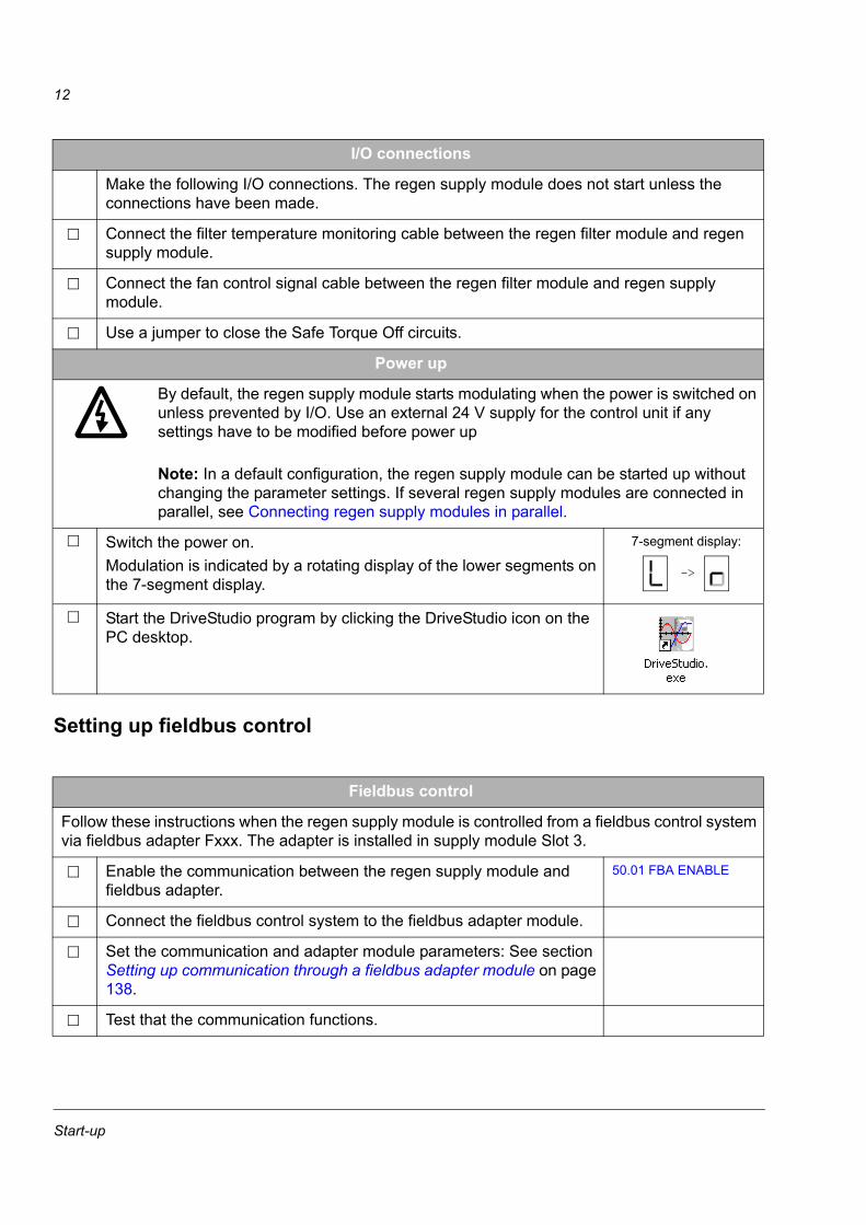
Setting up fieldbus control
I/O connections
Make the following I/O connections. The regen supply module does not start unless the connections have been made.
Connect the filter temperature monitoring cable between the regen filter module and regen supply module.
Connect the fan control signal cable between the regen filter module and regen supply module.
Use a jumper to close the Safe Torque Off circuits.
Power up
By default, the regen supply module starts modulating when the power is switched on unless prevented by I/O. Use an external 24 V supply for the control unit if any settings have to be modified before power up
Note: In a default configuration, the regen supply module can be started up without changing the parameter settings. If several regen supply modules are connected in parallel, see Connecting regen supply modules in parallel.
Switch the power on.Modulation is indicated by a rotating display of the lower segments on the 7-segment display.
7-segment display:
Start the DriveStudio program by clicking the DriveStudio icon on the PC desktop.
Fieldbus control
Follow these instructions when the regen supply module is controlled from a fieldbus control system via fieldbus adapter Fxxx. The adapter is installed in supply module Slot 3.
Enable the communication between the regen supply module and fieldbus adapter.
50.01 FBA ENABLE
Connect the fieldbus control system to the fieldbus adapter module.
Set the communication and adapter module parameters: See section Setting up communication through a fieldbus adapter module on page 138.
Test that the communication functions.
->

Start-up
13
Connecting regen supply modules in parallelConnecting regen supply modules in parallel
If several regen supply modules are connected in parallel, you must change the parameter settings in each regen supply module to configure the system for the parallel connection. Because the regen supply module starts modulating when the power is switched on, do not power up the system before the parameters have been set.If the JCUs are not externally powered, however, it is not possible to set the parameters without powering up the system, and therefore, you must prevent the regen supply module from starting when powering up the system.
Note: The released firmware (ULFI1020) also includes support for parallel connection of ACSM1-204 Regen Supplies. However, this is still in piloting mode because related ACSM1-204 types are not yet released for the sales at the date of publication of this manual.
Externally powered JCUsPower up the control board on each regen supply module.No externally powered JCUsDisconnect the filter temperature monitoring cable to prevent the regen supply module from starting during the power-up.
Set the parameters in each regen supply module:
Disable the earth fault detection by setting parameter 46.05 to 0 (No). 46.05 EARTH FAULT
Set parameter 60.01 to P.60.02 so you can manually set the DC reference value.Set the DC voltage reference value with parameter 60.02.Note: The DC voltage reference must be set to the same value in each of the parallel connected supply units.
60.01 DC REF SEL60.02 DC VOLT REF
Eliminate circulating current by setting parameter 64.01 to 1 (Enable). 64.01 CIRC CURR ELIM
Activate DC voltage control drooping by setting parameter 64.02 to 1 (Enable).
64.02 DC CTRL DROOP EN

Start-up
14

Supply module programming using PC tools
15
Supply module programming using PC tools
What this chapter containsThis chapter introduces the regen supply module programming using the DriveStudio and DriveSPC applications. For more information, see DriveStudio User Manual [3AFE68749026 (English)] and DriveSPC User Manual [3AFE68836590 (English)].
GeneralThe Regen Supply Control Program is divided into two parts:
• firmware program
• application program.
The firmware program performs the main control functions, including DC voltage and reactive power control, supply module logic (start/stop), I/O, communication and protection functions. Firmware functions are configured and programmed with parameters. The functions of the firmware program can be extended with application programming. Application programs are built out of function blocks.
The regen supply module supports two different programming methods:
• parameter programming
• application programming with function blocks (the blocks are based on the IEC-61131 standard).
Application program Firmware
Supply module logicI/O interfaceFieldbus interfaceProtectionsCommunication
Standard block library
Function block program
Regen Supply Control Program
Technology block library
Firmware blocks (parameter and signal interface)
Line filter Supply current
Supply module programming using PC tools
16
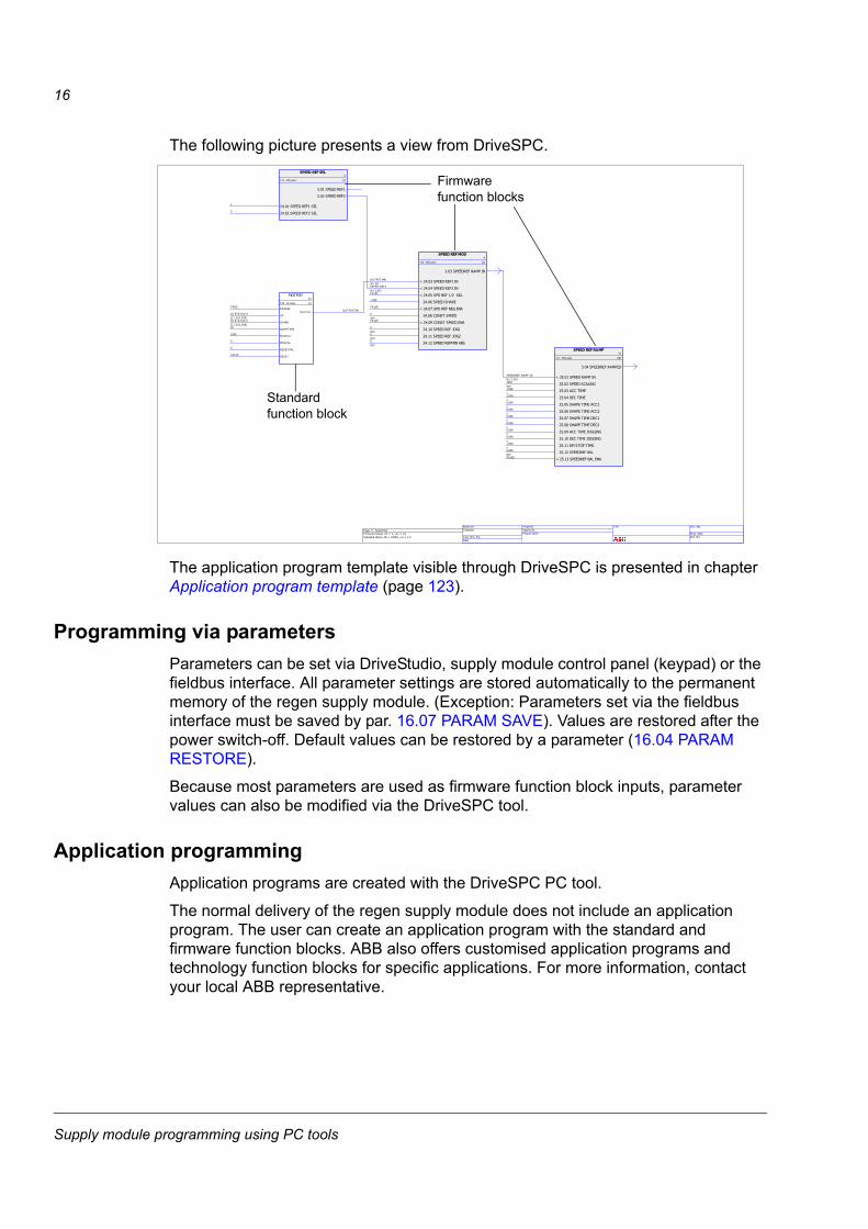
The following picture presents a view from DriveSPC.
The application program template visible through DriveSPC is presented in chapter Application program template (page 123).
Programming via parametersParameters can be set via DriveStudio, supply module control panel (keypad) or the fieldbus interface. All parameter settings are stored automatically to the permanent memory of the regen supply module. (Exception: Parameters set via the fieldbus interface must be saved by par. 16.07 PARAM SAVE). Values are restored after the power switch-off. Default values can be restored by a parameter (16.04 PARAM RESTORE).
Because most parameters are used as firmware function block inputs, parameter values can also be modified via the DriveSPC tool.
Application programmingApplication programs are created with the DriveSPC PC tool.
The normal delivery of the regen supply module does not include an application program. The user can create an application program with the standard and firmware function blocks. ABB also offers customised application programs and technology function blocks for specific applications. For more information, contact your local ABB representative.
SPEED REF SEL3
TL2 250 µsec (1)
24.01 SPEED REF1 SEL1
24.02 SPEED REF2 SEL0
3.01 SPEED REF1
3.02 SPEED REF2
SPEED REF MOD4
TL3 250 µsec (1)
< 24.03 SPEED REF1 INO UTPUT(44)
(6 / 44)
< 24.04 SPEED REF2 INSPEED REF2
(6 / 3.02)
< 24.05 SPD REF 1/2 SELFA LSE
24.06 SPEED SHARE1.000
< 24.07 SPD REF NEG ENAFA LSE
24.08 CONST SPEED0
rpm
< 24.09 CONST SPEED ENAFA LSE
24.10 SPEED REF JOG10
rpm
24.11 SPEED REF JOG20rpm
24.12 SPEED REFMIN ABS0rpm
3.03 SPEEDREF RAMP IN
SPEED REF RAMP31
TL7 500 µsec (18)
< 25.01 SPEED RAMP INSPEEDREF RAMP IN(6 / 3.03)
25.02 SPEED SCALING1500rpm
25.03 ACC TIME1.000
s
25.04 DEC TIME1.000
s
25.05 SHAPE TIME ACC10.000
s
25.06 SHAPE TIME ACC20.000
s
25.07 SHAPE TIME DEC10.000
s
25.08 SHAPE TIME DEC20.000
s
25.09 ACC TIME JOGGING0.000
s
25.10 DEC TIME JOGGING0.000
s
25.11 EM STOP TIME1.000s
25.12 SPEEDREF BAL0.000rpm
< 25.13 SPEEDREF BAL ENAFA LSE
3.04 SPEEDREF RAMPED
MOTPOT44
TL9 10 msec (1)
ENA BLETRUE
UPDI STATUS.4
(2 / 2.01.DI5)
DO WNDI STATUS.5
(2 / 2.01.DI6)
RAMPTIME10
MA XV A L1000
MINV AL0
RESETVA L0
RESETFA LSE
O UTPUTOUTPUT(44)
Page 6 Speed RefF irmware Library ID = 1, v er = 1.0Standard Library ID = 10000, v er = 1.0
Based onCustomer
Cust. Doc. No.Date
PreparedA pprov edProject name
Title Doc. des.
Resp. dept.Doc. No.
Standard function block
Firmwarefunction blocks

Supply module programming using PC tools
17
Function blocksThe application program uses three types of function blocks: firmware function blocks, standard function blocks and technology function blocks.
Firmware function blocks
Most of the firmware functions are represented as function blocks in the DriveSPC tool. Firmware function blocks are part of the regen supply module control firmware, and used as an interface between the application and firmware programs. Parameters in groups 10…99 are used as function block inputs and parameters in groups 1…9 as function block outputs. Firmware function blocks are presented in chapter Parameters and firmware blocks.
Standard function blocks (library)
Standard function blocks (e.g. ADD, AND) are used to create an executable application program. Blocks are based on the IEC-61131 standard. Standard function blocks are presented in ACSM1 Speed and Torque Control Program Firmware Manual (3AFE68848261 [English]).
Standard function block library is always included in the regen supply module delivery.
Technology function blocks
Several technology function block libraries are available for different types of applications. One technology library can be used at a time. Technology blocks are used in a similar way as the standard blocks.
Program executionThe application program is loaded to the permanent memory (non-volatile) of the memory unit (JMU). The execution of the downloaded program starts after the next reset of the supply module control board. The program is executed in real time on the same Central Processing Unit (CPU of the supply module control board) as the regen supply module firmware. The program is executed with two cyclical tasks. The time level for these tasks can be defined by the programmer (> 1ms).
Note: Because the firmware and application programs use the same CPU, the programmer must ensure that the regen supply module CPU is not overloaded. See parameter 1.21 CPU USAGE.
Supply module programming using PC tools
18
Operation modesThe DriveSPC tool offers the following operation modes:
Off-line
When the off-line mode is used without a regen supply module connection, the user can
• open a application program file (if exists).
• modify and save the application program.
• print the program pages.
When the off-line mode is used with a regen supply module(s) connection, the user can
• connect the selected regen supply module to DriveSPC.
• upload a application program from the connected regen supply module (an empty template which includes only the firmware blocks is available as default.)
• download the configured application program to the regen supply module and start the program execution. The downloaded program contains the function block program and the parameter values set in DriveSPC.
• remove the program from the connected regen supply module.
On-line
In the on-line mode, the user can
• modify firmware parameters (changes are stored directly to the regen supply module memory).
• modify application program parameters (i.e. parameters created in DriveSPC).
• monitor the actual values of all function blocks in real time.
Supply module control and features
19
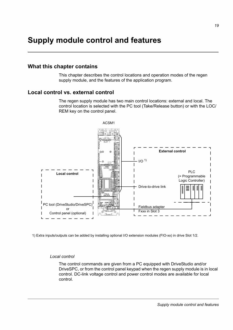
Supply module control and features
What this chapter containsThis chapter describes the control locations and operation modes of the regen supply module, and the features of the application program.
Local control vs. external controlThe regen supply module has two main control locations: external and local. The control location is selected with the PC tool (Take/Release button) or with the LOC/REM key on the control panel.
Local control
The control commands are given from a PC equipped with DriveStudio and/or DriveSPC, or from the control panel keypad when the regen supply module is in local control. DC-link voltage control and power control modes are available for local control.
PC tool (DriveStudio/DriveSPC)or
Control panel (optional)
1) Extra inputs/outputs can be added by installing optional I/O extension modules (FIO-xx) in drive Slot 1/2.
PLC (= Programmable Logic Controller)
External control
I/O 1)
Drive-to-drive link
Fieldbus adapterFxxx in Slot 3
Local control
ACSM1
Supply module control and features
20
Local control is mainly used during commissioning and maintenance. The control panel always overrides the external control signal sources when used in local control. Changing the control location to local can be disabled by parameter 16.01 LOCAL LOCK.
The user can select by a parameter (46.03 LOCAL CTRL LOSS) how the regen supply module reacts to a control panel or PC tool communication break.
External control
When the regen supply module is in external control, control commands (start/stop, reset, etc.) are given through the fieldbus interface (via an optional fieldbus adapter module), the I/O terminals (digital inputs), optional I/O extension modules or the drive-to-drive link. External references are given through the fieldbus interface, analogue inputs and drive-to-drive link.
Two external control locations, EXT1 and EXT2, are available. The user can select control signals (e.g. start/stop and reference) and control modes for both external control locations. Depending on the user selection, either EXT1 or EXT2 is active at a time. Selection between EXT1/EXT2 is done via digital inputs or fieldbus control word.
Voltage control in ACSM1-204The ACSM1-204 regen supply module is a four-quadrant switching-mode converter which means that the power flow through the converter is reversible. The regen supply module can control the power flow between the DC bus and the AC network.
In the DC voltage control mode, the regen supply module controls the power so that the DC bus voltage remains at its reference value. If the load is connected to the DC bus, the DC bus voltage control will transfer required power from the network or to the network so that a power balance between AC and DC sides is achieved.
By default, the converter controls the DC link voltage approximately to the peak value of the line-to-line voltage. The DC voltage reference can be set also higher with a parameter. Two line currents and the DC link voltage are measured and used for controlling.
The regen supply module can effectively control the power flow only if the DC bus voltage is higher or equal to the peak-value of the line-to-line mains voltage. To ensure this, the regen supply module has a voltage reserve controller that automatically raises the DC bus voltage if that is necessary to maintain the voltage reserve.
In the default configuration, the regen supply module operates with unity power factor. If needed, the regen supply module may generate or consume reactive power by setting reactive power reference to a non-zero value.

Supply module control and features
21
Control modes of the regen supply moduleACSM1-204 regen supply module has two control modes, DC voltage control mode and power control mode. In DC voltage control mode, the regen supply module controls the DC bus voltage according to given reference. In power control mode, the regen supply module controls AC power according to given power reference.
The DC voltage control mode is the typical operation mode of the regen supply module. The power control mode can be used if external power source is connected to the DC bus of the regen supply module. Control modes corresponding to different control locations can be selected in parameters 34.03, 34.05 and 34.07.
DC voltage control modeThe DC voltage reference can be selected in parameter 60.01. The default value is Internal, which means that the regen supply module generates the DC voltage reference internally according to the network voltage, operating point and desired voltage reserve (parameter 40.04).
Other sources of DC voltage reference include analog inputs, fieldbus and drive-to-drive link. Parameter 60.02 provides a constant reference source. In DC voltage reference choices other than Internal, the DC voltage controller controls the DC bus voltage to the selected reference. If the DC voltage reference is lower than what is needed to maintain desired voltage reserve, the regen supply module will internally increase the DC voltage reference so that the desired voltage reserve is maintained.
The desired voltage reserve can be set in parameter 40.04. The default value of 2% is suitable for most cases.
The DC voltage controller has a drooping feature that can be used if multiple regen supply modules are feeding the same DC bus. The drooping is enabled in parameter 64.02. The drooping rate is 20 V per nominal power. Thus, with nominal power regenerating the drooping raises the DC voltage by 20 V from its reference value.
The DC reference maximum and minimum values can be set with parameters 60.03 and 60.04. The DC reference ramp times per 100 V can be set with parameters 60.05 and 60.06.
Power control modeThe power reference source of the power control mode can be selected in parameter 62.01. By default, the power reference is given in parameter 62.02. Maximum and minimum limits of power reference can be set with parameters 62.03 and 62.04. Power reference ramp times per 1000 kW can be set with parameters 62.05 and 62.06.
The power control mode includes a feature for controlling over and undervoltage. In the power control mode, the DC bus voltage is determined by the balance of AC power which is set by the power reference and the external power fed to the DC link. The over- and undervoltage control modifies the output power of the regen supply module so that the DC bus voltage remains within the limits set by parameters 60.03 and 60.04.
Supply module control and features
22
Control features
Reactive power controlThe reactive power reference source can be selected in parameter 61.01. By default, the reactive power reference can be given in parameter 61.02. When the reference is positive, the regen supply module generates reactive power and appears as a capacitive component to the network. When the reference is negative, the regen supply module consumes reactive power and appears as an inductive component to the nerwork. If the current capacity of the regen supply module is fully used, the reactive power is reduced so that the required active power is delivered.
Note: Producing reactive power decreases available voltage reserve and may force the regen supply module to use a higher DC link voltage reference internally than is defined by the user.
Switching frequency referenceThe switching frequency reference can be set with parameter 40.02 SF REF. The default value is 3 kHz but it can be increased up to 16 kHz.
Note: The higher the switching frequency, the more losses it produces at power stage, the available current magnitude may be reduced.
Braking chopperThe built-in braking chopper of the drive can be used to handle the energy generated by a decelerating motor. When the braking chopper is enabled and a resistor is connected, the chopper will start conducting when the DC link voltage of the drive reaches 780 V. The maximum braking power is achieved at 840 V.
Parallel connectionACSM1-204 regen supply modules support redundant parallel connection of regen supply modules. Direct parallel connection without isolation transformers results in circulating zero-sequence current flow between paralleled units. In this case the circulating current elimination of parameter 64.01 must be enabled in all paralleled units.
In parallel configuration DC voltage controller drooping must be enabled in parameter 64.02 in all paralleled units. The same DC voltage reference must be used in all paralleled units.
If only one of the paralleled units is in the DC voltage control mode and the rest of them are in the power control mode, the DC voltage controller droop is not needed.
Paralleling regen supply modules without isolation transformers increases losses and may increase acoustic noise. Circulating current elimination decreases the maximum available current of the regen supply modules by 10%.

Supply module control and features
23
SynchronizationBefore the regen supply module can start modulation, it must synchronize itself with the network. To perform synchronization, the regen supply module needs network voltage, frequency and rotation direction data. The regen supply module can get network data automatically or you can give it manually. The ID run can also be used to get the user network data.
In the automatic mode, the regen supply module identifies the required network data at the start. Particularly in disturbed network conditions the repeatability and reliability of synchronization can be improved by using the user given data.
Automatic mode
The network data is identified automatically if necessary. The duration of identification is approximately 5…10 ms during which the unit takes 2…3 short current pulses from the network.
The automatic identification is done in the first start-up after the power-up and when ID run results have been cleared. In a unit with an externally powered JCU, the automatic identification is also done in the first start-up after the PU has been switched off.
User given data
Set the mains voltage, frequency and direction. User given data overrides any automatically identified data.
Partial user data is also supported. For example, by providing only the frequency eliminates the possible inaccuracies of automatic frequency identification. To eliminate the 5…10 ms delay of automatic identification, frequency and direction need to be set.
Values can be cleared by writing them to zero or by setting parameter 99.13 to Clear Result.
Network identification
Network identification can be used to get user network data. Group 99 can be used to initiate a network identification routine.
In network identification regen supply module synchronizes to the network with several current pulses and modulates for a few seconds. The identified values are written in parameters 63.01…63.03. Setting parameter 99.13 to Clear Result clears the user network data and sets synchronization to automatic mode.
Note: Synchronization to network may be unreliable if the current exceeds 50% of the nominal current at start-up.
ProtectionsThe regen supply module is protected against short circuit, overcurrent, overvoltage and undervoltage. The thermal protection scheme of the regen supply module includes a thermal model that estimates the critical power stage temperatures and limits AC current if that is necessary.
Supply module control and features
24
If excessive power is fed to the DC link, the regen supply module cannot keep the DC link voltage at its reference value and the voltage increases. If the DC link voltage reaches 880 V, the regen supply module trips on overvoltage. If the DC link voltage is increased beyond that, the regen supply module may be damaged.
If excessive power is taken from the DC link, the regen supply module cannot reduce the AC current. When the current capability of the regen supply module is exceeded, it can no longer control the DC link voltage and the power is transferred through the freewheeling diodes of the power stage. Excessive current causes the regen supply module to trip on overcurrent but it cannot reduce the current flow. Therefore, excessive power taken from the DC link may damage the regen supply module.

Default connections of the control unit
25
Default connections of the control unit
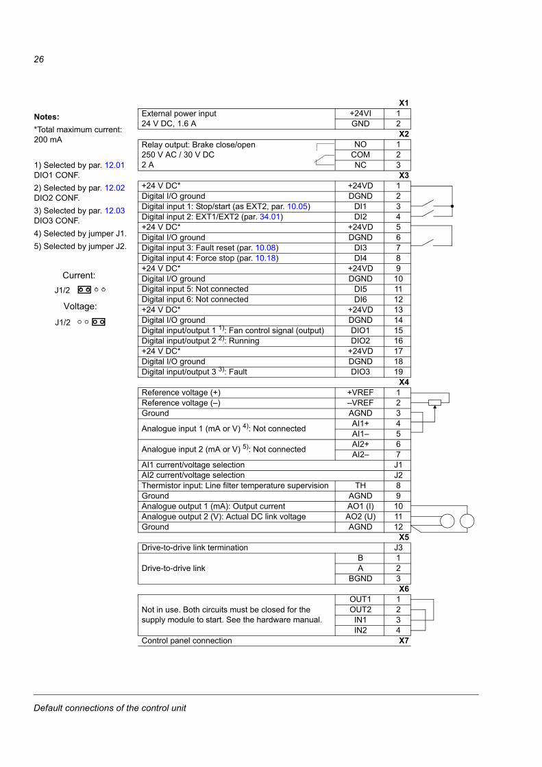
What this chapter containsThis chapter shows the default control connections of the JCU Control Unit.
More information on the connectivity of the JCU is given in the Hardware Manual of the regen supply module.
Default connections of the control unit
26
Notes:*Total maximum current: 200 mA
1) Selected by par. 12.01 DIO1 CONF.2) Selected by par. 12.02 DIO2 CONF.3) Selected by par. 12.03 DIO3 CONF.4) Selected by jumper J1.5) Selected by jumper J2.
X1External power input24 V DC, 1.6 A
+24VI 1GND 2
X2Relay output: Brake close/open250 V AC / 30 V DC2 A
NO 1COM 2NC 3
X3+24 V DC* +24VD 1Digital I/O ground DGND 2Digital input 1: Stop/start (as EXT2, par. 10.05) DI1 3Digital input 2: EXT1/EXT2 (par. 34.01) DI2 4+24 V DC* +24VD 5Digital I/O ground DGND 6Digital input 3: Fault reset (par. 10.08) DI3 7Digital input 4: Force stop (par. 10.18) DI4 8+24 V DC* +24VD 9Digital I/O ground DGND 10Digital input 5: Not connected DI5 11Digital input 6: Not connected DI6 12+24 V DC* +24VD 13Digital I/O ground DGND 14Digital input/output 1 1): Fan control signal (output) DIO1 15Digital input/output 2 2): Running DIO2 16+24 V DC* +24VD 17Digital I/O ground DGND 18Digital input/output 3 3): Fault DIO3 19
X4Reference voltage (+) +VREF 1Reference voltage (–) –VREF 2Ground AGND 3
Analogue input 1 (mA or V) 4): Not connected AI1+ 4AI1– 5
Analogue input 2 (mA or V) 5): Not connected AI2+ 6AI2– 7
AI1 current/voltage selection J1AI2 current/voltage selection J2Thermistor input: Line filter temperature supervision TH 8Ground AGND 9Analogue output 1 (mA): Output current AO1 (I) 10Analogue output 2 (V): Actual DC link voltage AO2 (U) 11Ground AGND 12
X5Drive-to-drive link termination J3
Drive-to-drive linkB 1A 2
BGND 3X6
Not in use. Both circuits must be closed for the supply module to start. See the hardware manual.
OUT1 1OUT2 2
IN1 3IN2 4
Control panel connection X7
Current:
Voltage:
J1/2
J1/2
Parameters and firmware blocks
27
Parameters and firmware blocks
What this chapter containsThis chapter lists and describes the parameters provided by the firmware.
Types of parametersParameters are user-adjustable operation instructions of the drive (groups 10…99). There are four basic types of parameters: Actual signals, value parameters, value pointer parameters and bit pointer parameters.
Actual signal
Type of parameter that is the result of a measurement or calculation by the drive. Actual signals can be monitored, but not adjusted, by the user. Actual signals are typically contained within parameter groups 1…9.
For additional actual signal data, e.g. update cycles and fieldbus equivalents, see chapter Parameter data.
Value parameter
A value parameter has a fixed set of choices or a setting range.
Example 1: You can select how the supply reacts when an earth fault or current unbalance is detected in the supply or the supply cable by selecting an option from the selection list of parameter 46.05.
Example 2: To define the constant value for DC voltage reference, set parameter 60.02 to an appropriate value.
Value pointer parameter
A value pointer parameter points to the value of another parameter. The source parameter is given in format P.xx.yy, where xx = Parameter group; yy = Parameter index. In addition, many value pointer parameters have a set of pre-selected choices.
Example: Converter current signal, 1.05 CURRENT PERC, is connected to analogue output AO1 by setting parameter 15.01 AO1 PTR to value P.01.05.
Bit pointer parameter
A bit pointer parameter points to the value of a bit in another parameter, or can be fixed to 0 (FALSE) or 1 (TRUE). In addition, many bit pointer parameters have a set of pre-selected choices.
When adjusting a bit pointer parameter on the optional control panel, CONST is selected in order to fix the value to 0 (displayed as “C.FALSE”) or 1 (“C.TRUE”). POINTER is selected to define a source from another parameter.
A pointer value is given in format P.xx.yy.zz, where xx = Parameter group, yy = Parameter index, zz = Bit number.
Parameters and firmware blocks
28
Example: Parameter 10.08 FAULT RESET SEL is used to select the source parameter for the external fault reset signal.
Note: Pointing to a nonexisting bit will be interpreted as 0 (FALSE).
For additional parameter data, e.g. update cycles and fieldbus equivalents, see chapter Parameter data.
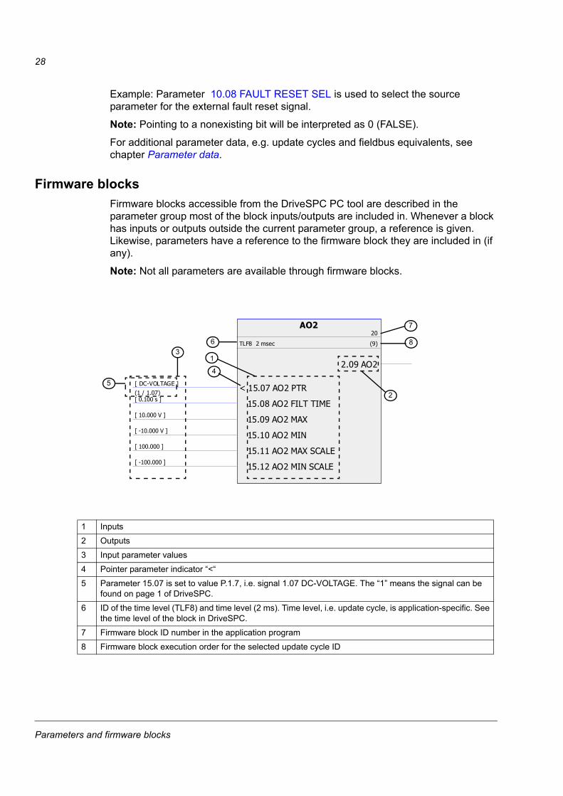
Firmware blocksFirmware blocks accessible from the DriveSPC PC tool are described in the parameter group most of the block inputs/outputs are included in. Whenever a block has inputs or outputs outside the current parameter group, a reference is given. Likewise, parameters have a reference to the firmware block they are included in (if any).
Note: Not all parameters are available through firmware blocks.
AO220
TLF8 2 msec (9)
< 15.07 AO2 PTR[ DC-VOLTAGE ]
(1 / 1.07)
15.08 AO2 FILT TIME[ 0.100 s ]
15.09 AO2 MAX[ 10.000 V ]
15.10 AO2 MIN[ -10.000 V ]
15.11 AO2 MAX SCALE[ 100.000 ]
15.12 AO2 MIN SCALE[ -100.000 ]
2.09 AO2
1 Inputs
2 Outputs
3 Input parameter values
4 Pointer parameter indicator “<“
5 Parameter 15.07 is set to value P.1.7, i.e. signal 1.07 DC-VOLTAGE. The “1” means the signal can be found on page 1 of DriveSPC.
6 ID of the time level (TLF8) and time level (2 ms). Time level, i.e. update cycle, is application-specific. See the time level of the block in DriveSPC.
7 Firmware block ID number in the application program
8 Firmware block execution order for the selected update cycle ID
2
36
7
8
45
1
Parameters and firmware blocks
29
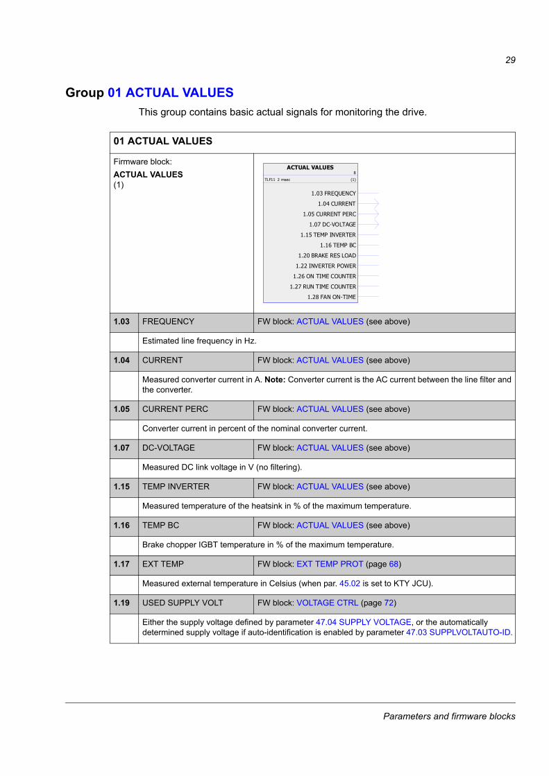
Group 01 ACTUAL VALUESThis group contains basic actual signals for monitoring the drive.
0101 ACTUAL VALUES
Firmware block:ACTUAL VALUES(1)
1.03 FREQUENCY FW block: ACTUAL VALUES (see above)
Estimated line frequency in Hz.
1.04 CURRENT FW block: ACTUAL VALUES (see above)
Measured converter current in A. Note: Converter current is the AC current between the line filter and the converter.
1.05 CURRENT PERC FW block: ACTUAL VALUES (see above)
Converter current in percent of the nominal converter current.
1.07 DC-VOLTAGE FW block: ACTUAL VALUES (see above)
Measured DC link voltage in V (no filtering).
1.15 TEMP INVERTER FW block: ACTUAL VALUES (see above)
Measured temperature of the heatsink in % of the maximum temperature.
1.16 TEMP BC FW block: ACTUAL VALUES (see above)
Brake chopper IGBT temperature in % of the maximum temperature.
1.17 EXT TEMP FW block: EXT TEMP PROT (page 68)
Measured external temperature in Celsius (when par. 45.02 is set to KTY JCU).
1.19 USED SUPPLY VOLT FW block: VOLTAGE CTRL (page 72)
Either the supply voltage defined by parameter 47.04 SUPPLY VOLTAGE, or the automatically determined supply voltage if auto-identification is enabled by parameter 47.03 SUPPLVOLTAUTO-ID.
ACTUAL VALUES8
TLF11 2 msec (1)
1.03 FREQUENCY
1.04 CURRENT
1.05 CURRENT PERC
1.07 DC-VOLTAGE
1.15 TEMP INVERTER
1.16 TEMP BC
1.20 BRAKE RES LOAD
1.22 INVERTER POWER
1.26 ON TIME COUNTER
1.27 RUN TIME COUNTER
1.28 FAN ON-TIME

Parameters and firmware blocks
30
1.20 BRAKE RES LOAD FW block: ACTUAL VALUES (see above)
Estimated temperature of the braking resistor. The value is given in percent of the temperature the resistor reaches when loaded with the power defined by parameter 48.04 BR POWER MAX CNT.
1.21 CPU USAGE FW block: None
Microprocessor load in percent.
1.22 INVERTER POWER FW block: ACTUAL VALUES (see above)
Calculated line-side converter power in kilowatts. Positive value: Power flow from the supply network to the intermediate circuit. Negative value: Power flow from the intermediate circuit to the supply network.
1.26 ON TIME COUNTER FW block: ACTUAL VALUES (see above)
This counter runs when the regen supply module is powered. The counter can be reset using the DriveStudio tool. On-time is measured in hours.
1.27 RUN TIME COUNTER FW block: ACTUAL VALUES (see above)
Run time counter. The counter runs when the regen supply module modulates. The counter can be reset using the DriveStudio tool. Run-time is measured in hours.
1.28 FAN ON-TIME FW block: None
On-time counter of the power unit’s cooling fan. Fan on-time is measured in hours.
Parameters and firmware blocks
31
Group 02 I/O VALUESThis group contains information on the I/Os of the drive.
0202 I/O VALUES
2.01 DI STATUS FW block: DI (page 49)
Status word of the digital inputs. Example: 000001 = DI1 is on, DI2 to DI6 are off.
2.02 RO STATUS FW block: RO (page 49)
Status of relay output. 1 = RO is energized.
2.03 DIO STATUS FW blocks: DIO1 (page 47), DIO2 (page 47), DIO3 (page 47)
Status word of digital inputs/outputs DIO1…3. Example: 001 = DIO1 is on, DIO2 and DIO3 are off.
2.04 AI1 FW block: AI1 (page 51)
Analogue input AI1 value in V or mA. The type is selected with jumper J1 on the JCU Control Unit.
2.05 AI1 SCALED FW block: AI1 (page 51)
Scaled value of analogue input AI1. See parameters 13.04 AI1 MAX SCALE and 13.05 AI1 MIN SCALE.
2.06 AI2 FW block: AI2 (page 52)
Analogue input AI2 value in V or mA. The type is selected with jumper J2 on the JCU Control Unit.
2.07 AI2 SCALED FW block: AI2 (page 52)
Scaled value of analogue input AI2. See parameters 13.09 AI2 MAX SCALE and 13.10 AI2 MIN SCALE.
2.08 AO1 FW block: AO1 (page 55)
Analogue output AO1 value in mA
2.09 AO2 FW block: AO2 (page 56)
Analogue output AO2 value in V
2.10 DIO2 FREQ IN FW block: DIO2 (page 47)
Frequency input value in Hz when DIO2 is used as frequency input (12.02 DIO2 CONF is set to (2) FREQ INPUT).
2.11 DIO3 FREQ OUT FW block: DIO3 (page 47)
Frequency output value in Hz when DIO3 is used as frequency output (12.03 DIO3 CONF is set to (2) FREQ OUTPUT).

Parameters and firmware blocks
32
2.12 FBA MAIN CW FW block: FIELDBUS (page 75)
Control Word for fieldbus communication.Log. = Logical combination (i.e. Bit AND/OR Selection parameter). Par. = Selection parameter. See State diagram on page 143.
Bit Name Val. Information Log. Par.0 STOP* 1 Modulation ends immediately. Note: Simultaneous
STOP and START commands result in a stop com-mand.
OR 10.02,10.03,10.05,10.060 No operation
1 START 1 Start. Note: Simultaneous STOP and START commands result in a stop command.
OR 10.02,10.03,10.05,10.06
0 No operation
2 STPMODE EM OFF*
1 Emergency OFF2 (bit 0 must be 1): Drive is stopped by cutting off the motor power supply (the inverter IGBTs are blocked). The motor coasts to stop. The drive will restart only with the next rising edge of the start signal when the run enable signal is on.
AND -
0 No operation3…6 Reserved7 RUN
ENABLE1 Activate run enable. AND 10.090 Activate run disable.
8 RESET 0->1 Fault reset if an active fault exists. OR 10.08other No operation
9…10 Reserved11 REMOTE
CMD1 Fieldbus control enabled - -0 Fieldbus control disabled
12…14 Reserved15 EXT1/EXT2 1 Switch to external control location EXT2. OR 34.01
0 Switch to external control location EXT1.16 REQ
STARTINH1 Activate start inhibit. - -0 No start inhibit
17 LOCAL CTL 1 Request local control for Control Word. Used when the drive is controlled via PC tool or panel.- Panel or PC tool: Transfer to local control.
- -
0 Request external control.18…27 Reserved28 CW B28 Freely programmable control bits. - -29 CW B2930 CW B3031 CW B31
Parameters and firmware blocks
33
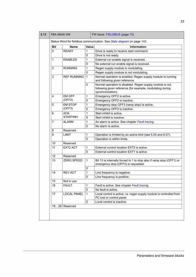
2.13 FBA MAIN SW FW block: FIELDBUS (page 75)
Status Word for fieldbus communication. See State diagram on page 143.
Bit Name Value Information0 READY 1 Drive is ready to receive start command.
0 Drive is not ready.1 ENABLED 1 External run enable signal is received.
0 No external run enable signal is received.2 RUNNING 1 Regen supply module is modulating.
0 Regen supply module is not modulating.3 REF RUNNING 1 Normal operation is enabled. Regen supply module is running
and following given reference.0 Normal operation is disabled. Regen supply module is not
following given reference (for example, modulating during synchronization).
4 EM OFF (OFF2)
1 Emergency OFF2 is active.0 Emergency OFF2 is inactive.
5 EM STOP (OFF3)
1 Emergency stop OFF3 (ramp stop) is active.0 Emergency OFF3 is inactive.
6 ACK STARTINH
1 Start inhibit is active.0 Start inhibit is inactive.
7 ALARM 1 An alarm is active. See chapter Fault tracing.0 No alarm is active.
8 Reserved9 LIMIT 1 Operation is limited by an active limit (see 6.05 and 6.07).
0 Operation is within limits.10 Reserved11 EXT2 ACT 1 External control location EXT2 is active.
0 External control location EXT1 is active.12 Reserved13 ZERO SPEED 1 Bit 13 is internally forced to 1 to stop also if ramp stop (OFF1) or
emergency stop (OFF3) is requested.0
14 REV ACT 1 Line frequency is negative.0 Line frequency is positive.
15 Not in use16 FAULT 1 Fault is active. See chapter Fault tracing.
0 No fault is active.17 LOCAL PANEL 1 Local control is active, i.e. regen supply module is controlled from
PC tool or control panel.0 Local control is inactive.
18…26 Reserved
Parameters and firmware blocks
34
2.13 FBA MAIN SW (continued from previous page)
2.14 FBA MAIN REF1 FW block: FIELDBUS (page 75)
Scaled fieldbus reference 1. See parameter 50.04 FBA REF1 SCALE.
2.15 FBA MAIN REF2 FW block: FIELDBUS (page 75)
Scaled fieldbus reference 2. See parameter 50.05 FBA REF2 SCALE.
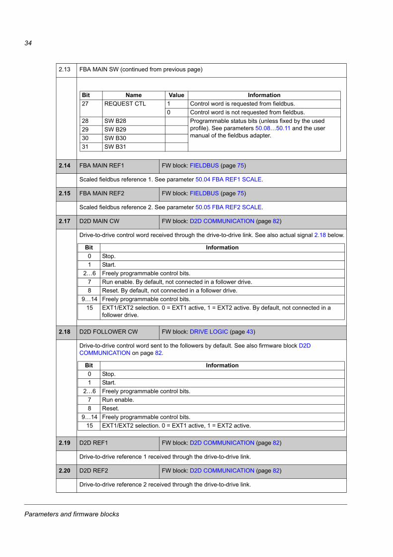
2.17 D2D MAIN CW FW block: D2D COMMUNICATION (page 82)
Drive-to-drive control word received through the drive-to-drive link. See also actual signal 2.18 below.
2.18 D2D FOLLOWER CW FW block: DRIVE LOGIC (page 43)
Drive-to-drive control word sent to the followers by default. See also firmware block D2D COMMUNICATION on page 82.
2.19 D2D REF1 FW block: D2D COMMUNICATION (page 82)
Drive-to-drive reference 1 received through the drive-to-drive link.
2.20 D2D REF2 FW block: D2D COMMUNICATION (page 82)
Drive-to-drive reference 2 received through the drive-to-drive link.
Bit Name Value Information27 REQUEST CTL 1 Control word is requested from fieldbus.
0 Control word is not requested from fieldbus.28 SW B28 Programmable status bits (unless fixed by the used
profile). See parameters 50.08…50.11 and the user manual of the fieldbus adapter.
29 SW B2930 SW B3031 SW B31
Bit Information0 Stop.1 Start.
2…6 Freely programmable control bits.7 Run enable. By default, not connected in a follower drive.8 Reset. By default, not connected in a follower drive.
9…14 Freely programmable control bits.15 EXT1/EXT2 selection. 0 = EXT1 active, 1 = EXT2 active. By default, not connected in a
follower drive.
Bit Information0 Stop.1 Start.
2…6 Freely programmable control bits.7 Run enable.8 Reset.
9…14 Freely programmable control bits.15 EXT1/EXT2 selection. 0 = EXT1 active, 1 = EXT2 active.
Parameters and firmware blocks
35
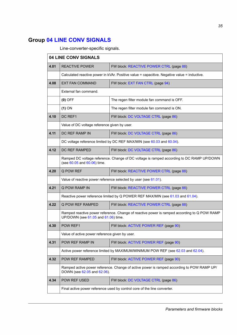
Group 04 LINE CONV SIGNALSLine-converter-specific signals.
04 LINE CONV SIGNALS
4.01 REACTIVE POWER FW block: REACTIVE POWER CTRL (page 88)
Calculated reactive power in kVAr. Positive value = capacitive. Negative value = inductive.
4.08 EXT FAN COMMAND FW block: EXT FAN CTRL (page 94)
External fan command.
(0) OFF The regen filter module fan command is OFF.
(1) ON The regen filter module fan command is ON.
4.10 DC REF1 FW block: DC VOLTAGE CTRL (page 86)
Value of DC voltage reference given by user.
4.11 DC REF RAMP IN FW block: DC VOLTAGE CTRL (page 86)
DC voltage reference limited by DC REF MAX/MIN (see 60.03 and 60.04).
4.12 DC REF RAMPED FW block: DC VOLTAGE CTRL (page 86)
Ramped DC voltage reference. Change of DC voltage is ramped according to DC RAMP UP/DOWN (see 60.05 and 60.06) time.
4.20 Q POW REF FW block: REACTIVE POWER CTRL (page 88)
Value of reactive power reference selected by user (see 61.01).
4.21 Q POW RAMP IN FW block: REACTIVE POWER CTRL (page 88)
Reactive power reference limited by Q POWER REF MAX/MIN (see 61.03 and 61.04).
4.22 Q POW REF RAMPED FW block: REACTIVE POWER CTRL (page 88)
Ramped reactive power reference. Change of reactive power is ramped according to Q POW RAMP UP/DOWN (see 61.05 and 61.06) time.
4.30 POW REF1 FW block: ACTIVE POWER REF (page 90)
Value of active power reference given by user.
4.31 POW REF RAMP IN FW block: ACTIVE POWER REF (page 90)
Active power reference limited by MAXIMUM/MINIMUM POW REF (see 62.03 and 62.04).
4.32 POW REF RAMPED FW block: ACTIVE POWER REF (page 90)
Ramped active power reference. Change of active power is ramped according to POW RAMP UP/DOWN (see 62.05 and 62.06).
4.34 POW REF USED FW block: DC VOLTAGE CTRL (page 86)
Final active power reference used by control core of the line converter.

Parameters and firmware blocks
36
Group 06 DRIVE STATUSStatus words.
0606 DRIVE STATUS
6.01 STATUS WORD 1 FW block: DRIVE LOGIC (page 43)
Status word 1.
Bit Name Val. Information0 READY 1 Drive is ready to receive start command.
0 Drive is not ready.1 ENABLED 1 External run enable signal is received.
0 No external run enable signal is received.2 STARTED 1 Drive has received start command.
0 Drive has not received start command.3 RUNNING 1 Drive is modulating.
0 Drive is not modulating.4 EM OFF (OFF2) 1 Emergency OFF2 is active.
0 Emergency OFF2 is inactive.5 EM STOP
(OFF3)1 Emergency stop OFF3 (ramp stop) is active.0 Emergency OFF3 is inactive.
6 ACK STARTINH 1 Start inhibit is active.0 Start inhibit is inactive.
7 ALARM 1 An alarm is active. See chapter Fault tracing.0 No alarm
8 EXT2 ACT 1 External control EXT2 is active.0 External control EXT1 is active.
9 LOCAL FB 1 Fieldbus local control is active.0 Fieldbus local control is inactive.
10 FAULT 1 A fault is active. See chapter Fault tracing.0 No fault
11 LOCAL PANEL 1 Local control is active, i.e. drive is controlled from PC tool or control panel.
0 Local control is inactive.12…15 Reserved
Parameters and firmware blocks
37
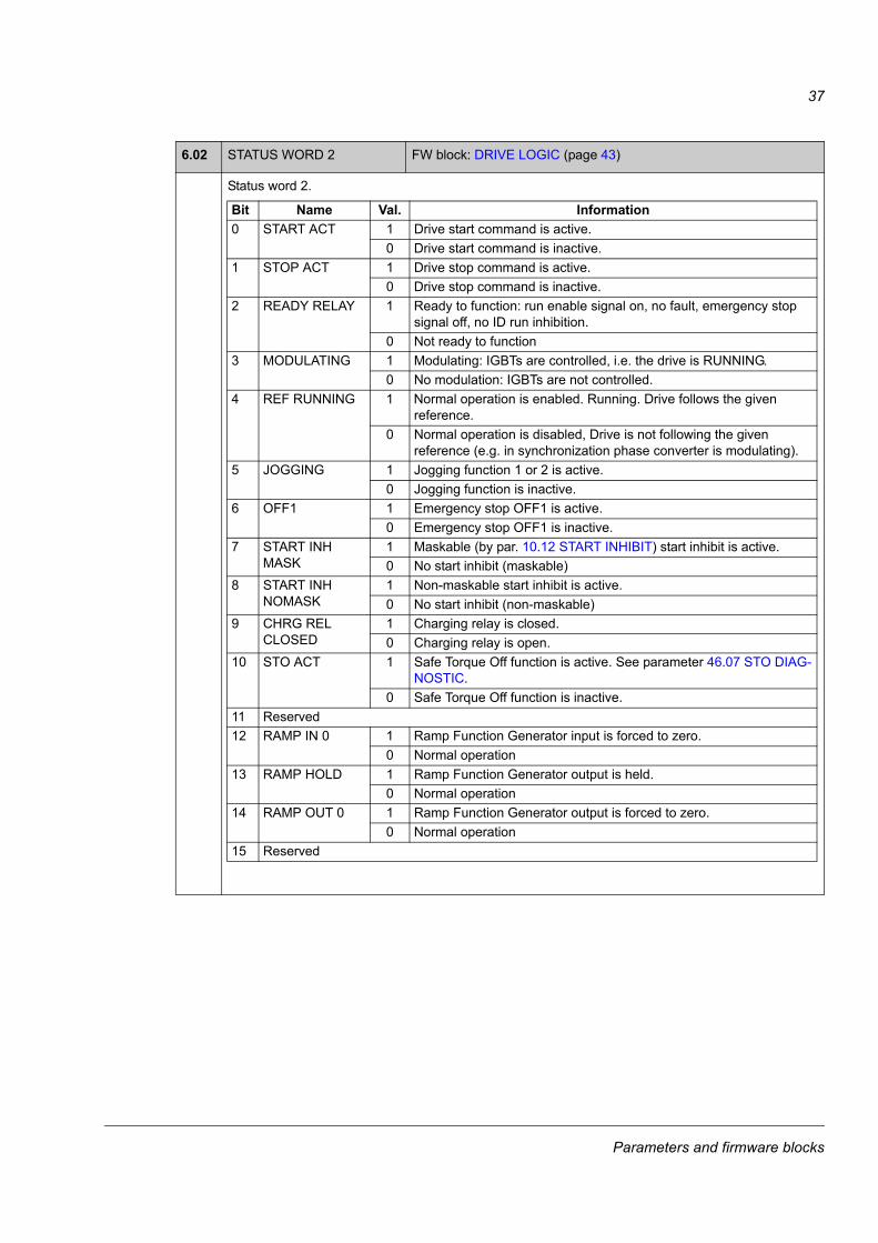
6.02 STATUS WORD 2 FW block: DRIVE LOGIC (page 43)
Status word 2.
Bit Name Val. Information0 START ACT 1 Drive start command is active.
0 Drive start command is inactive.1 STOP ACT 1 Drive stop command is active.
0 Drive stop command is inactive.2 READY RELAY 1 Ready to function: run enable signal on, no fault, emergency stop
signal off, no ID run inhibition.0 Not ready to function
3 MODULATING 1 Modulating: IGBTs are controlled, i.e. the drive is RUNNING.0 No modulation: IGBTs are not controlled.
4 REF RUNNING 1 Normal operation is enabled. Running. Drive follows the given reference.
0 Normal operation is disabled, Drive is not following the given reference (e.g. in synchronization phase converter is modulating).
5 JOGGING 1 Jogging function 1 or 2 is active.0 Jogging function is inactive.
6 OFF1 1 Emergency stop OFF1 is active.0 Emergency stop OFF1 is inactive.
7 START INH MASK
1 Maskable (by par. 10.12 START INHIBIT) start inhibit is active.0 No start inhibit (maskable)
8 START INH NOMASK
1 Non-maskable start inhibit is active.0 No start inhibit (non-maskable)
9 CHRG REL CLOSED
1 Charging relay is closed.0 Charging relay is open.
10 STO ACT 1 Safe Torque Off function is active. See parameter 46.07 STO DIAG-NOSTIC.
0 Safe Torque Off function is inactive.11 Reserved12 RAMP IN 0 1 Ramp Function Generator input is forced to zero.
0 Normal operation13 RAMP HOLD 1 Ramp Function Generator output is held.
0 Normal operation14 RAMP OUT 0 1 Ramp Function Generator output is forced to zero.
0 Normal operation15 Reserved

Parameters and firmware blocks
38
6.05 LIMIT WORD 1 FW block: DRIVE LOGIC (page 43)
Limit word 1.
6.07 LC LIM STATUS FW block: DRIVE LOGIC (page 43)
Line converter control limitation status word.
Bit Name Val. Information0 LIMIT 1 Combined limitation status of FA and LC. Set if any bit in 6.05 or
6.07 is set.1 UDC REF MIN
LIM1 DC voltage reference at minimum limit.
2 UDC REF MAX LIM
1 DC voltage reference at maximum limit.
3 UDC REF INCREASED
1 DC voltage reference increased by LC based on 40.04 VOLTAGE RESERVE.
4 Q REF MIN LIM 1 Reactive power reference at minimum limit.5 Q REF MAX LIM 1 Reactive power reference at maximum limit. 6 Q REF POS LIM 1 Capacitive power limited by LC. 7 Q REF NEG LIM 1 Inductive power limited by LC. 8…15 Reserved
Bit Name Val. Information0 UNDERVOLTAGE 1 DC voltage controller is limiting power based on 60.04 (only in
POWER control mode).1 OVERVOLTAGE 1 DC voltage controller is limiting power based on 60.05 (only in
POWER control mode).2 MINIMUM POWER 1 Power reference minimum limit is active. Limit is defined by
parameter 62.04 MINIMUM POW REF.3 MAXIMUM POWER 1 Power reference maximum limit is active. Limit is defined by
parameter 62.03 MAXIMUM POW REF.4 ACTIVE CURRENT 1 Active current is limited.5 REACTIVE CUR-
RENT1 Reactive current is limited.
6…8 Reserved9 I2MAX CURRENT 1 Inverter maximum output current limit is active.10 USER CURRENT 1 Current limit defined by parameter 20.05 MAXIMUM CURRENT
is active.11 Reserved12 INU OVERTEMP 1 Current is limited based on thermal model.13 INU OVERLOAD 1 Current is limited based on thermal model.14 Reserved

Parameters and firmware blocks
39
6.12 OP MODE ACK FW block: REFERENCE CTRL (page 66)
Operation mode acknowledge.
(0) STOPPED Converter is not modulating or is not ready to follow given reference.
(1) DC VOLTAGE DC voltage reference is followed.
(2) ACTIVE POWER Power reference is followed in Power control mode.
(3) INTERNAL REF DC voltage control mode is active and input reference 4.10 DC REF1 is zero. DC voltage level is controlled based on parameter 40.04 VOLTAGE RESERVE.
6.13 SUPERV STATUS FW block: NONE
Supervision status word. Bits 0 and 2 reflect the status of supervisory functions 1 and 3, respectively. The functions are configured in parameter group 33 SUPERVISION.

Parameters and firmware blocks
40
Group 08 ALARMS & FAULTSSignals containing alarm and fault information.
0808 ALARMS & FAULTS
8.01 ACTIVE FAULT FW block: FAULT FUNCTIONS (page 70)
Fault code of the latest (active) fault.
8.02 LAST FAULT FW block: FAULT FUNCTIONS (page 70)
Fault code of the 2nd latest fault.
8.03 FAULT TIME HI FW block: FAULT FUNCTIONS (page 70)
Time (real time or power-on time) at which the active fault occurred in format dd.mm.yy (=day.month.year).
8.04 FAULT TIME LO FW block: FAULT FUNCTIONS (page 70)
Time (real time or power-on time) at which the active fault occurred in format hh.mm.ss (hours.minutes.seconds).
8.05 ALARM WORD 1 FW block: FAULT FUNCTIONS (page 70)
Alarm word 1. For possible causes and remedies, see chapter Fault tracing.
Bit Alarm0…2 Reserved3 SAFE TORQUE OFF4 STO MODE CHANGE5 EXT TEMPERATURE6 EMERGENCY OFF7 RUN ENABLE8 ID-RUN9 EMERGENCY STOP10 Reserved11 BR OVERHEAT12 BC OVERHEAT 13 DEVICE OVERTEMP 14 INTBOARD OVERTEMP15 BC MOD OVERTEMP

Parameters and firmware blocks
41
8.06 ALARM WORD 2 FW block: FAULT FUNCTIONS (page 70)
Alarm word 2. For possible causes and remedies, see chapter Fault tracing.
8.07 ALARM WORD 3 FW block: FAULT FUNCTIONS (page 70)
Alarm word 3. For possible causes and remedies, see chapter Fault tracing.
8.08 ALARM WORD 4 FW block: FAULT FUNCTIONS (page 70)
Alarm word 4. For possible causes and remedies, see chapter Fault tracing.
Bit Alarm0 IGBT OVERTEMP1 FIELDBUS COMM2 LOCAL CTRL LOSS3 AI SUPERVISION4…15 Reserved
Bit Alarm0 Reserved1 D2D COMMUNICATION2 D2D BUF OVLOAD3 PS COMM4 RESTORE5 CUR MEAS CALIBRATION6 Reserved7 EARTH FAULT8…9 Reserved10 D2D CONFIG11…15 Reserved
Bit Alarm0 OPTION COMM LOSS1…15 Reserved
Parameters and firmware blocks
42
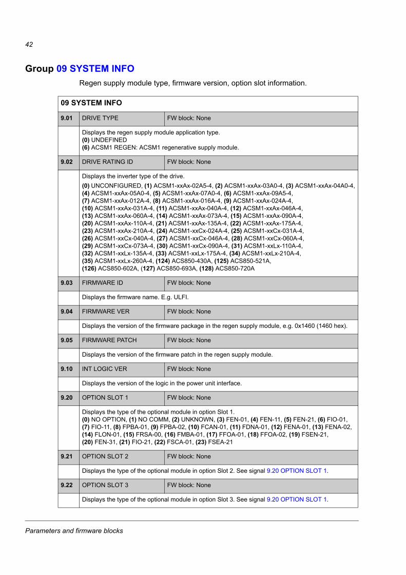
Group 09 SYSTEM INFORegen supply module type, firmware version, option slot information.
09 SYSTEM INFO
9.01 DRIVE TYPE FW block: None
Displays the regen supply module application type.(0) UNDEFINED(6) ACSM1 REGEN: ACSM1 regenerative supply module.
9.02 DRIVE RATING ID FW block: None
Displays the inverter type of the drive.(0) UNCONFIGURED, (1) ACSM1-xxAx-02A5-4, (2) ACSM1-xxAx-03A0-4, (3) ACSM1-xxAx-04A0-4, (4) ACSM1-xxAx-05A0-4, (5) ACSM1-xxAx-07A0-4, (6) ACSM1-xxAx-09A5-4, (7) ACSM1-xxAx-012A-4, (8) ACSM1-xxAx-016A-4, (9) ACSM1-xxAx-024A-4, (10) ACSM1-xxAx-031A-4, (11) ACSM1-xxAx-040A-4, (12) ACSM1-xxAx-046A-4, (13) ACSM1-xxAx-060A-4, (14) ACSM1-xxAx-073A-4, (15) ACSM1-xxAx-090A-4, (20) ACSM1-xxAx-110A-4, (21) ACSM1-xxAx-135A-4, (22) ACSM1-xxAx-175A-4, (23) ACSM1-xxAx-210A-4, (24) ACSM1-xxCx-024A-4, (25) ACSM1-xxCx-031A-4, (26) ACSM1-xxCx-040A-4, (27) ACSM1-xxCx-046A-4, (28) ACSM1-xxCx-060A-4, (29) ACSM1-xxCx-073A-4, (30) ACSM1-xxCx-090A-4, (31) ACSM1-xxLx-110A-4, (32) ACSM1-xxLx-135A-4, (33) ACSM1-xxLx-175A-4, (34) ACSM1-xxLx-210A-4, (35) ACSM1-xxLx-260A-4, (124) ACS850-430A, (125) ACS850-521A,(126) ACS850-602A, (127) ACS850-693A, (128) ACS850-720A
9.03 FIRMWARE ID FW block: None
Displays the firmware name. E.g. ULFI.
9.04 FIRMWARE VER FW block: None
Displays the version of the firmware package in the regen supply module, e.g. 0x1460 (1460 hex).
9.05 FIRMWARE PATCH FW block: None
Displays the version of the firmware patch in the regen supply module.
9.10 INT LOGIC VER FW block: None
Displays the version of the logic in the power unit interface.
9.20 OPTION SLOT 1 FW block: None
Displays the type of the optional module in option Slot 1.(0) NO OPTION, (1) NO COMM, (2) UNKNOWN, (3) FEN-01, (4) FEN-11, (5) FEN-21, (6) FIO-01, (7) FIO-11, (8) FPBA-01, (9) FPBA-02, (10) FCAN-01, (11) FDNA-01, (12) FENA-01, (13) FENA-02, (14) FLON-01, (15) FRSA-00, (16) FMBA-01, (17) FFOA-01, (18) FFOA-02, (19) FSEN-21, (20) FEN-31, (21) FIO-21, (22) FSCA-01, (23) FSEA-21
9.21 OPTION SLOT 2 FW block: None
Displays the type of the optional module in option Slot 2. See signal 9.20 OPTION SLOT 1.
9.22 OPTION SLOT 3 FW block: None
Displays the type of the optional module in option Slot 3. See signal 9.20 OPTION SLOT 1.
Parameters and firmware blocks
43
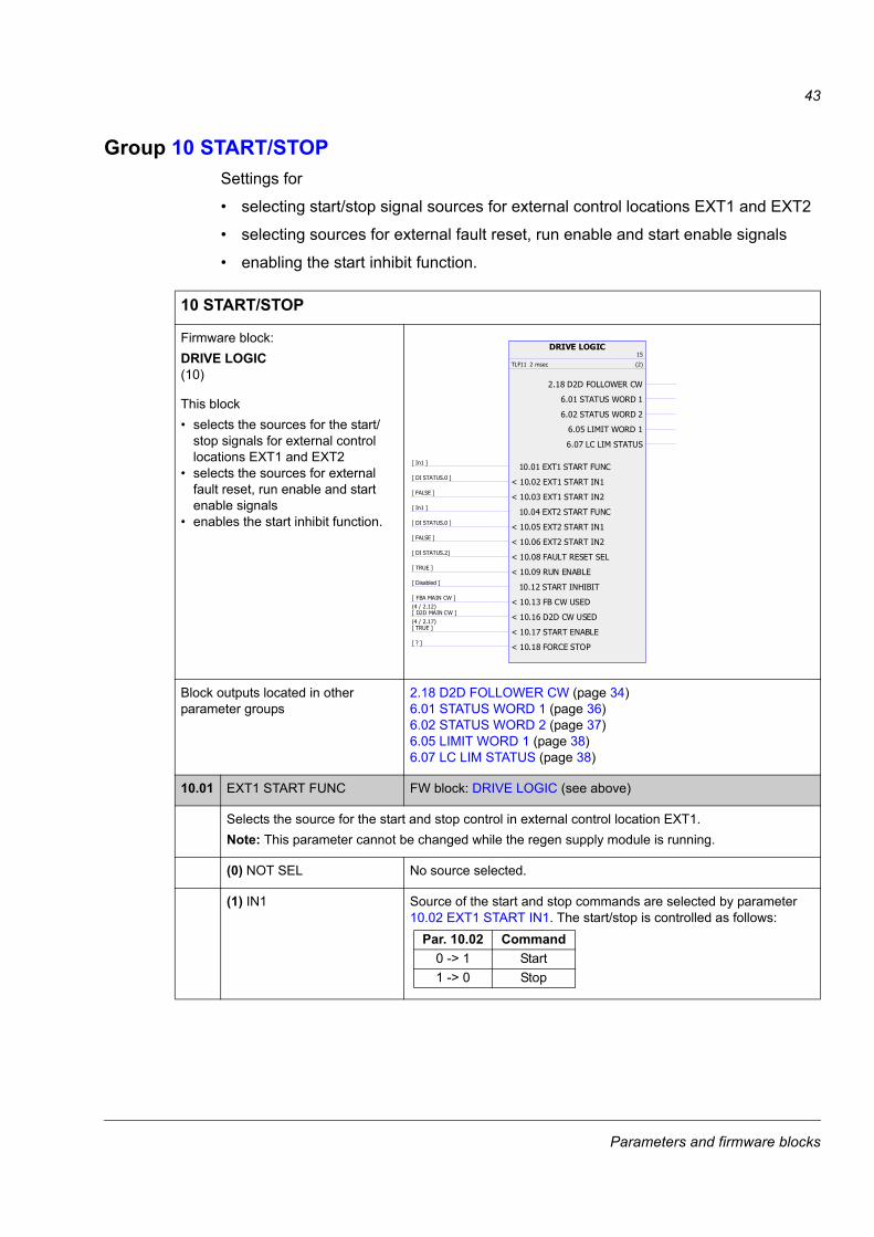
Group 10 START/STOPSettings for
• selecting start/stop signal sources for external control locations EXT1 and EXT2
• selecting sources for external fault reset, run enable and start enable signals
• enabling the start inhibit function.
10 START/STOP
Firmware block:DRIVE LOGIC(10)
This block• selects the sources for the start/
stop signals for external control locations EXT1 and EXT2
• selects the sources for external fault reset, run enable and start enable signals
• enables the start inhibit function.
Block outputs located in other parameter groups
2.18 D2D FOLLOWER CW (page 34)6.01 STATUS WORD 1 (page 36)6.02 STATUS WORD 2 (page 37)6.05 LIMIT WORD 1 (page 38)6.07 LC LIM STATUS (page 38)
10.01 EXT1 START FUNC FW block: DRIVE LOGIC (see above)
Selects the source for the start and stop control in external control location EXT1. Note: This parameter cannot be changed while the regen supply module is running.
(0) NOT SEL No source selected.
(1) IN1 Source of the start and stop commands are selected by parameter 10.02 EXT1 START IN1. The start/stop is controlled as follows:
DRIVE LOGIC15
TLF11 2 msec (2)
10.01 EXT1 START FUNC[ In1 ]
< 10.02 EXT1 START IN1[ DI STATUS.0 ]
< 10.03 EXT1 START IN2[ FALSE ]
10.04 EXT2 START FUNC[ In1 ]
< 10.05 EXT2 START IN1[ DI STATUS.0 ]
< 10.06 EXT2 START IN2[ FALSE ]
< 10.08 FAULT RESET SEL[ DI STATUS.2]
< 10.09 RUN ENABLE[ TRUE ]
10.12 START INHIBIT[ Disabled ]
< 10.13 FB CW USED[ FBA MAIN CW ]
(4 / 2.12)
< 10.16 D2D CW USED[ D2D MAIN CW ]
(4 / 2.17)
< 10.17 START ENABLE[ TRUE ]
< 10.18 FORCE STOP[ ? ]
2.18 D2D FOLLOWER CW
6.01 STATUS WORD 1
6.02 STATUS WORD 2
6.05 LIMIT WORD 1
6.07 LC LIM STATUS
Par. 10.02 Command0 -> 1 Start1 -> 0 Stop

Parameters and firmware blocks
44
(2) 3-WIRE Source of the start and stop commands are selected by parameters 10.02 EXT1 START IN1 and 10.03 EXT1 START IN2. The start/stop is controlled as follows:
(3) FBA Start and stop control from the source selected by parameter 10.13 FB CW USED.
(4) D2D Start and stop control from another regen supply module via D2D Control Word.
10.02 EXT1 START IN1 FW block: DRIVE LOGIC (see above)
Selects the source 1 for the start and stop commands in external control location EXT1. See parameter 10.01 EXT1 START FUNC selections (1) IN1 and (2) 3-WIRE.Note: This parameter cannot be changed while the regen supply module is running.
Bit pointer: Group, index and bit
10.03 EXT1 START IN2 FW block: DRIVE LOGIC (see above)
Selects the source 2 for the start and stop commands in external control location EXT1. See parameter 10.01 EXT1 START FUNC selection (2) 3-WIRE.Note: This parameter cannot be changed while the regen supply module is running.
Bit pointer: Group, index and bit
10.04 EXT2 START FUNC FW block: DRIVE LOGIC (see above)
Selects the source for the start and stop control in external control location EXT2.Note: This parameter cannot be changed while the regen supply module is running.
(0) NOT SEL No source selected.
(1) IN1 Source of the start and stop commands are selected by parameter 10.05 EXT2 START IN1. The start/stop is controlled as follows:
(2) 3-WIRE Source of the start and stop commands are selected by parameters 10.05 EXT2 START IN1 and 10.06 EXT2 START IN2. The start/stop is controlled as follows:
(3) FBA Start and stop control from the source selected by parameter 10.13 FB CW USED.
Par. 10.02 Par. 10.03 Command0 -> 1 1 StartAny 1 -> 0 StopAny 0 Stop
Par. 10.05 Command0 -> 1 Start1 -> 0 Stop
Par. 10.05 Par. 10.06 Command0 -> 1 1 StartAny 1 -> 0 StopAny 0 Stop

Parameters and firmware blocks
45
(4) D2D Start and stop control from another regen supply module via D2D Control Word (par. 2.17 D2D MAIN CW).
10.05 EXT2 START IN1 FW block: DRIVE LOGIC (see above)
Selects the source 1 for the start and stop commands in external control location EXT2. See parameter 10.04 EXT2 START FUNC selections (1) IN1 and (2) 3-WIRE.Note: This parameter cannot be changed while the regen supply module is running.
Bit pointer: Group, index and bit
10.06 EXT2 START IN2 FW block: DRIVE LOGIC (see above)
Selects the source 2 for the start and stop commands in external control location EXT2. See parameter 10.04 EXT2 START FUNC selection (2) 3-WIRE.Note: This parameter cannot be changed while the regen supply module is running.
Bit pointer: Group, index and bit
10.08 FAULT RESET SEL FW block: DRIVE LOGIC (see above)
Selects the source for the external fault reset signal. The signal resets the regen supply module after a fault trip if the cause of the fault no longer exists. 1 = Fault reset.
Bit pointer: Group, index and bit
10.09 RUN ENABLE FW block: DRIVE LOGIC (see above)
Selects the source for the run enable signal. If the run enable signal is switched off, the regen supply module will not start or stops if the regen supply module is running. 1 = Run enable.Note: This parameter cannot be changed while the regen supply module is running.
Bit pointer: Group, index and bit
10.12 START INHIBIT FW block: DRIVE LOGIC (see above)
Enables the start inhibit function. The start inhibit function prevents regen supply module restart (i.e. protects against unexpected start) if• regen supply module trips on a fault and fault is reset.• run enable signal activates while the start command is active. See parameter 10.09 RUN ENABLE.• control changes from local to remote.• external control switches from EXT1 to EXT2 or from EXT2 to EXT1.An active start inhibit can be reset with a stop command.Note that in certain applications it is necessary to allow the regen supply module to restart.
(0) DISABLED Start inhibit function disabled.
(1) ENABLED Start inhibit function enabled.
10.13 FB CW USED FW block: DRIVE LOGIC (see above)
Selects the source for the control word when fieldbus (FBA) is selected as the external start and stop control location (see parameters 10.01 EXT1 START FUNC and 10.04 EXT2 START FUNC). By default, the source is parameter 2.12 FBA MAIN CW.Note: This parameter cannot be changed while the regen supply module is running.
Value pointer: Group and index

Parameters and firmware blocks
46
10.16 D2D CW USED FW block: DRIVE LOGIC (see above)
Selects the source for the control word for drive-to-drive communication. By default, the source is parameter 2.17 D2D MAIN CW.
Value pointer: Group and index
10.17 START ENABLE FW block: DRIVE LOGIC (see above)
Selects the source for the start enable signal. If the start enable signal is switched off, the regen supply module will not start or stops if the regen supply module is running. 1 = Start enable.Note: This parameter cannot be changed while the regen supply module is running.
Bit pointer: Group, index and bit
10.18 FORCE STOP FW block: DRIVE LOGIC (see above)
Stops modulation and prevents starting while active. Note: Force stop also prevents the start command in local control.

Parameters and firmware blocks
47
Group 12 DIGITAL IOSettings for the digital inputs and outputs, and the relay output.
1212 DIGITAL IO
Firmware block:DIO1(6)
Selects whether DIO1 is used as a digital input or as a digital output and connects an actual signal to the digital output. The block also shows the DIO status.
Block outputs located in other parameter groups
2.03 DIO STATUS (page 31)
Firmware block:DIO2(7)
Selects whether DIO2 is used as a digital or frequency input or as a digital output and connects an actual signal to the digital output. The block also shows the DIO status.Frequency input can be scaled with standard function blocks. See chapter Standard function blocks.
Block outputs located in other parameter groups
2.03 DIO STATUS (page 31)2.10 DIO2 FREQ IN (page 31)
Firmware block:DIO3(8)
Selects whether DIO3 is used as a digital input or as a digital/frequency output, connects an actual signal to the digital/frequency output and scales the frequency output. The block also shows the DIO status.
Block outputs located in other parameter groups
2.03 DIO STATUS (page 31)2.11 DIO3 FREQ OUT (page 31)
12.01 DIO1 CONF FW block: DIO1 (see above)
Selects whether DIO1 is used as a digital input or as a digital output.
(0) OUTPUT DIO1 is used as a digital output.
DIO112
TLF8 2 msec (3)
12.01 DIO1 CONF(Drive value)
< 12.04 DIO1 OUT PTR(Drive value)
2.03 DIO STATUS2.03
Bit 0
DIO213
TLF8 2 msec (4)
12.02 DIO2 CONF(Drive value)
< 12.05 DIO2 OUT PTR(Drive value)
12.14 DIO2 F MAX(Drive value)
12.15 DIO2 F MIN(Drive value)
12.16 DIO2 F MAX SCALE(Drive value)
12.17 DIO2 F MIN SCALE(Drive value)
2.03 DIO STATUS2.03
Bit 1
2.10 DIO2 FREQ IN
DIO314
TLF8 2 msec (5)
12.03 DIO3 CONF[ Output ]
< 12.06 DIO3 OUT PTR[ STATUS WORD 1.10 ]
< 12.07 DIO3 F OUT PTR[ DC-VOLTAGE ]
(1 / 1.07)
12.08 DIO3 F MAX[ TBA ]
12.09 DIO3 F MIN[ 3 Hz ]
12.10 DIO3 F MAX SCALE[ 1500 ]
12.11 DIO3 F MIN SCALE[ 0 ]
2.03 DIO STATUS2.03
Bit 2
2.11 DIO3 FREQ OUT
Parameters and firmware blocks
48
(1) INPUT DIO1 is used as a digital input.
12.02 DIO2 CONF FW block: DIO2 (see above)
Selects whether DIO2 is used as a digital input, as a digital output or as a frequency input.
(0) OUTPUT DIO2 is used as a digital output.
(1) INPUT DIO2 is used as a digital input.
(2) FREQ INPUT DIO2 is used as a frequency input.
12.03 DIO3 CONF FW block: DIO3 (see above)
Selects whether DIO3 is used as a digital input, as a digital output or as a frequency output.
(0) OUTPUT DIO2 is used as a digital output.
(1) INPUT DIO2 is used as a digital input.
(2) FREQ OUTPUT DIO2 is used as a frequency output.
12.04 DIO1 OUT PTR FW block: DIO1 (see above)
Selects a regen supply module signal to be connected to digital output DIO1 (when 12.01 DIO1 CONF is set to (0) OUTPUT).
Bit pointer: Group, index and bit
12.05 DIO2 OUT PTR FW block: DIO2 (see above)
Selects a regen supply module signal to be connected to digital output DIO2 (when 12.02 DIO2 CONF is set to (0) OUTPUT).
Bit pointer: Group, index and bit
12.06 DIO3 OUT PTR FW block: DIO3 (see above)
Selects a regen supply module signal to be connected to digital output DIO3 (when 12.03 DIO3 CONF is set to (0) OUTPUT).
Bit pointer: Group, index and bit
12.07 DIO3 F OUT PTR FW block: DIO3 (see above)
Selects a regen supply module signal to be connected to frequency output (when 12.03 DIO3 CONF is set to (2) FREQ OUTPUT).
Value pointer: Group and index
12.08 DIO3 F MAX FW block: DIO3 (see above)
Defines the maximum value for frequency output (when 12.03 DIO3 CONF is set to (2) FREQ OUTPUT).
3…32768 Hz Maximum DIO3 output frequency.

Parameters and firmware blocks
49
12.09 DIO3 F MIN FW block: DIO3 (see above)
Defines the minimum value for frequency output (when 12.03 DIO3 CONF is set to (2) FREQ OUTPUT).
3…32768 Hz Minimum DIO3 output frequency.
12.10 DIO3 F MAX SCALE FW block: DIO3 (see above)
Defines the real value that corresponds to the maximum frequency output value defined by parameter 12.08 DIO3 F MAX.
0…32768 Real value corresponding to value of parameter 12.08.
12.11 DIO3 F MIN SCALE FW block: DIO3 (see above)
Defines the real value that corresponds to the minimum frequency output value defined by parameter 12.09 DIO3 F MIN. See parameter 12.10 DIO3 F MAX SCALE.
0…32768 Real value corresponding to value of parameter 12.09.
Firmware block:RO(5)
Connects an actual signal to the relay output. The block also shows the relay output status.
Block outputs located in other parameter groups
2.02 RO STATUS (page 31)
12.12 RO1 OUT PTR FW block: RO (see above)
Selects a regen supply module signal to be connected to relay output RO1.
Bit pointer: Group, index and bit
Firmware block:DI(4)
Shows the status of the digital inputs. Inverts the status of any DI if desired.
Block outputs located in other parameter groups
2.01 DI STATUS (page 31)
DIO3 (Hz)
DIO3 (real)12.09
12.11 12.10
DIO3 (Hz)
DIO3 (real)
12.08
12.09
12.10 12.11
12.08
RO11
TLF8 2 msec (2)
< 12.12 RO1 OUT PTR[ BRAKE COMMAND.0 ]
2.02 RO STATUS
DI10
TLF8 2 msec (1)
12.13 DI INVERT MASK[ 00 0000 ]
2.01 DI STATUS
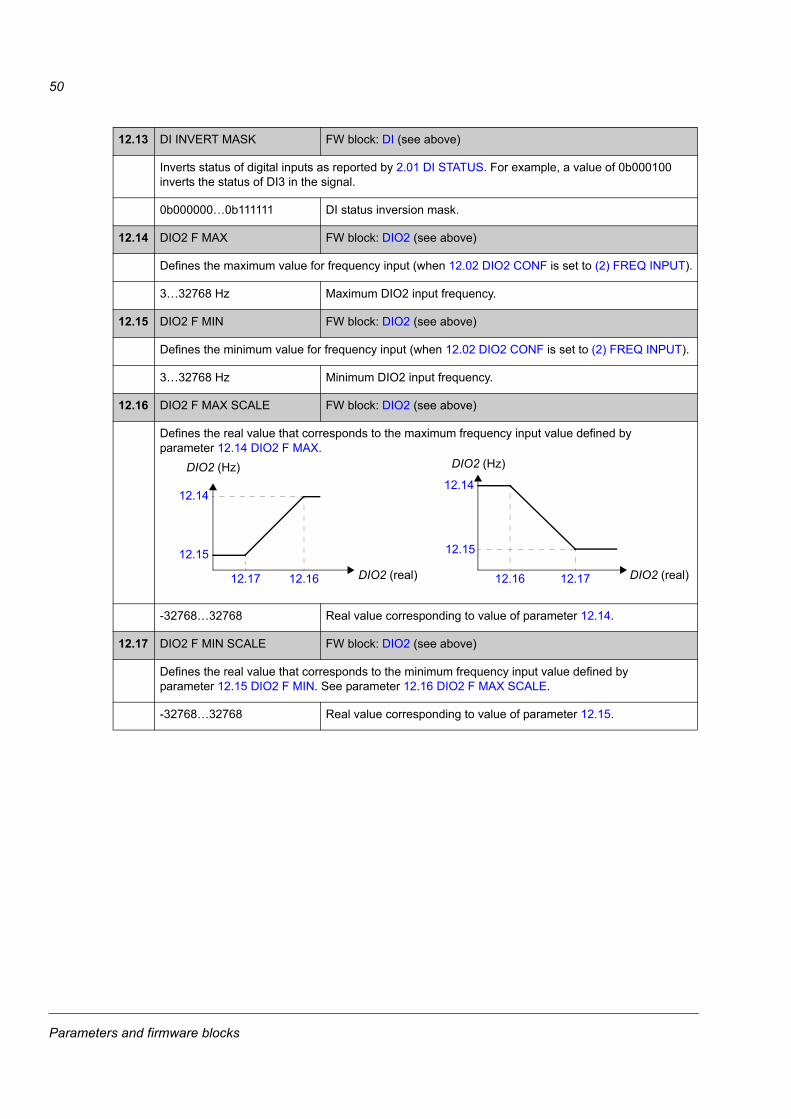
Parameters and firmware blocks
50
12.13 DI INVERT MASK FW block: DI (see above)
Inverts status of digital inputs as reported by 2.01 DI STATUS. For example, a value of 0b000100 inverts the status of DI3 in the signal.
0b000000…0b111111 DI status inversion mask.
12.14 DIO2 F MAX FW block: DIO2 (see above)
Defines the maximum value for frequency input (when 12.02 DIO2 CONF is set to (2) FREQ INPUT).
3…32768 Hz Maximum DIO2 input frequency.
12.15 DIO2 F MIN FW block: DIO2 (see above)
Defines the minimum value for frequency input (when 12.02 DIO2 CONF is set to (2) FREQ INPUT).
3…32768 Hz Minimum DIO2 input frequency.
12.16 DIO2 F MAX SCALE FW block: DIO2 (see above)
Defines the real value that corresponds to the maximum frequency input value defined by parameter 12.14 DIO2 F MAX.
-32768…32768 Real value corresponding to value of parameter 12.14.
12.17 DIO2 F MIN SCALE FW block: DIO2 (see above)
Defines the real value that corresponds to the minimum frequency input value defined by parameter 12.15 DIO2 F MIN. See parameter 12.16 DIO2 F MAX SCALE.
-32768…32768 Real value corresponding to value of parameter 12.15.
12.14
12.15
12.14
12.15
12.1712.1612.1612.17 DIO2 (real)
DIO2 (Hz)
DIO2 (real)
DIO2 (Hz)

Parameters and firmware blocks
51
Group 13 ANALOGUE INPUTSSettings for the analogue inputs.
The regen supply module offers two programmable analogue inputs, AI1 and AI2. Both inputs can be used either as a voltage or a current input (-11…11 V or -22…22 mA). The input type is selected with jumpers J1 and J2 respectively on the JCU Control Unit.
The inaccuracy of the analogue inputs is 1% of the full scale range and the resolution is 11 bits (+ sign). The hardware filter time constant is approximately 0.25 ms.
Analogue inputs can be used as the source for DC voltage/power and reactive power reference.
Analogue input supervision can be added with standard function blocks. See chapter Standard function blocks.
13 ANALOGUE INPUTS
Firmware block:AI1(12)
Filters and scales the analogue input AI1 signal and selects the AI1 supervision. Also shows the value of the input.
Block outputs located in other parameter groups
2.04 AI1 (page 31)2.05 AI1 SCALED (page 31)
13.01 AI1 FILT TIME FW block: AI1 (see above)
Defines the filter time constant for analogue input AI1.
Note: The signal is also filtered due to the signal interface hardware (approximately 0.25 ms time constant). This cannot be changed by any parameter.
0…30 s Filter time constant for AI1.
13.02 AI1 MAX FW block: AI1 (see above)
Defines the maximum value for analogue input AI1. The type is selected with jumper J1 on the JCU Control Unit.
-11…11 V / -22…22 mA Maximum AI1 input value.
AI117
TLF8 2 msec (6)
13.01 AI1 FILT TIME[ 0.000 s ]
13.02 AI1 MAX[ 10.000 mA ]
13.03 AI1 MIN[ -10.000 mA ]
13.04 AI1 MAX SCALE[ 1500.000 ]
13.05 AI1 MIN SCALE[ -1500.000 ]
2.04 AI1
2.05 AI1 SCALED
63
%
100
Tt
Filtered signal
Unfiltered signal O = I · (1 - e-t/T)
I = filter input (step)O = filter outputt = timeT = filter time constant

Parameters and firmware blocks
52
13.03 AI1 MIN FW block: AI1 (see above)
Defines the minimum value for analogue input AI1. The type is selected with jumper J1 on the JCU Control Unit.
-11…11 V / -22…22 mA Minimum AI1 input value.
13.04 AI1 MAX SCALE FW block: AI1 (see above)
Defines the real value that corresponds to the maximum analogue input value defined by parameter 13.02 AI1 MAX.
-32768…32768 Real value corresponding to value of parameter 13.02.
13.05 AI1 MIN SCALE FW block: AI1 (see above)
Defines the real value that corresponds to the minimum analogue input value defined by parameter 13.03 AI1 MIN. See parameter 13.04 AI1 MAX SCALE.
-32768…32768 Real value corresponding to value of parameter 13.03.
Firmware block:AI2(13)
Filters and scales the analogue input AI2 signal and selects the AI2 supervision. Also shows the value of the input.
Block outputs located in other parameter groups
2.06 AI2 (page 31)2.07 AI2 SCALED (page 31)
13.06 AI2 FILT TIME FW block: AI2 (see above)
Defines the filter time constant for analogue input AI2. See parameter 13.01 AI1 FILT TIME.
0…30 s Filter time constant for AI2.
13.07 AI2 MAX FW block: AI2 (see above)
Defines the maximum value for analogue input AI2. The type is selected with jumper J2 on the JCU Control Unit.
AI (mA / V)
AI (real)
13.0413.05
13.03
13.02
AI218
TLF8 2 msec (7)
13.06 AI2 FILT TIME[ 0.000 s ]
13.07 AI2 MAX[ 10.000 mA ]
13.08 AI2 MIN[ -10.000 mA ]
13.09 AI2 MAX SCALE[ 100.000 ]
13.10 AI2 MIN SCALE[ -100.000 ]
2.06 AI2
2.07 AI2 SCALED

Parameters and firmware blocks
53
-11…11 V / -22…22 mA Maximum AI2 input value.
13.08 AI2 MIN FW block: AI2 (see above)
Defines the minimum value for analogue input AI2. The type is selected with jumper J2 on the JCU Control Unit.
-11…11 V / -22…22 mA Minimum AI2 input value.
13.09 AI2 MAX SCALE FW block: AI2 (see above)
Defines the real value that corresponds to the maximum analogue input value defined by parameter 13.07 AI2 MAX.
-32768…32768 Real value corresponding to value of parameter 13.07.
13.10 AI2 MIN SCALE FW block: AI2 (see above)
Defines the real value that corresponds to the minimum analogue input value defined by parameter 13.08 AI2 MIN. See parameter 13.09 AI2 MAX SCALE.
-32768…32768 Real value corresponding to value of parameter 13.08.
13.11 AITUNE FW block: None
Triggers the AI tuning function.Connect the signal to the input and select the appropriate tuning function.
(0) NO ACTION AI tune is not activated.
(1) AI1 MIN TUNE Current analogue input AI1 signal value is set as minimum value for AI1, parameter 13.03 AI1 MIN. The value reverts back to (0) NO ACTION automatically.
(2) AI1 MAX TUNE Current analogue input AI1 signal value is set as maximum value for AI1, parameter 13.02 AI1 MAX. The value reverts back to (0) NO ACTION automatically.
(3) AI2 MIN TUNE Current analogue input AI2 signal value is set as minimum value for AI2, parameter 13.08 AI2 MIN. The value reverts back to (0) NO ACTION automatically.
(4) AI2 MAX TUNE Current analogue input AI2 signal value is set as maximum value for AI2, parameter 13.07 AI2 MAX. The value reverts back to (0) NO ACTION automatically.
AI (mA / V)
AI (real)
13.0913.10
13.08
13.07
Parameters and firmware blocks
54
13.12 AI SUPERVISION FW block: None
Selects how the regen supply module reacts when analogue input signal limit is reached. The limit is selected by parameter 13.13 AI SUPERVIS ACT.
(0) NO No action taken.
(1) FAULT The regen supply module trips on fault AI SUPERVISION.
13.13 AI SUPERVIS ACT FW block: None
Selects the analogue input signal supervision limit.
Example: If parameter value is set to 0010 (bin), bit 1 AI1>max is selected.
0b0000…0b1111 AI1/AI2 signal supervision selection.
Bit Supervision selected by parameter 13.12 AI SUPERVISION is activated if0 AI1<min AI1 signal value falls below the value defined by equation:
par. 13.03 AI1 MIN - 0.5 mA or V
1 AI1>max AI1 signal value exceeds the value defined by equation:par. 13.02 AI1 MAX + 0.5 mA or V
2 AI2<min AI2 signal value falls below the value defined by equation:par. 13.08 AI2 MIN - 0.5 mA or V
3 AI2>min AI2 signal value exceeds the value defined by equation:par. 13.07 AI2 MAX + 0.5 mA or V
Parameters and firmware blocks
55
Group 15 ANALOGUE OUTPUTSSettings for the analogue outputs.The regen supply module offers two programmable analogue outputs: one current output AO1 (0…20 mA) and one voltage output AO2 (-10…10 V).
The resolution of the analogue outputs is 11 bits (+ sign) and the inaccuracy is 2% of the full scale range.
The analogue output signals can be proportional to DC voltage, output frequency, output current, power, etc. It is possible to write a value to an analogue output through a serial communication link (e.g. fieldbus link).
1515 ANALOGUE OUTPUTS
Firmware block:AO1(14)
Connects an actual signal to analogue output AO1, and filters and scales the output signal. Also shows the value of the output.
Block outputs located in other parameter groups
2.08 AO1 (page 31)
15.01 AO1 PTR FW block: AO1 (see above)
Selects a regen supply module signal to be connected to analogue output AO1.
Value pointer: Group and index
15.02 AO1 FILT TIME FW block: AO1 (see above)
Defines the filtering time constant for analogue output AO1.
Note: The signal is also filtered due to the signal interface hardware (approximately 0.5 ms time constant). This cannot be changed by any parameter.
0…30 s Filter time constant for AO1.
15.03 AO1 MAX FW block: AO1 (see above)
Defines the maximum value for analogue output AO1.
0…22.7 mA Maximum AO1 output value.
AO119
TLF8 2 msec (8)
< 15.01 AO1 PTR[ CURRENT PERC ]
(1 / 1.05)
15.02 AO1 FILT TIME[ 0.100 s ]
15.03 AO1 MAX[ 20.000 mA ]
15.04 AO1 MIN[ 4.000 mA ]
15.05 AO1 MAX SCALE[ 100.000 ]
15.06 AO1 MIN SCALE[ 0.000 ]
2.08 AO1
63
%
100
Tt
Filtered signal
Unfiltered signal O = I · (1 - e-t/T)
I = filter input (step)O = filter outputt = timeT = filter time constant

Parameters and firmware blocks
56
15.04 AO1 MIN FW block: AO1 (see above)
Defines the minimum value for analogue output AO1.
0…22.7 mA Minimum AO1 output value.
15.05 AO1 MAX SCALE FW block: AO1 (see above)
Defines the real value that corresponds to the maximum analogue output value defined by parameter 15.03 AO1 MAX.
-32768…32767 Real value corresponding to value of parameter 15.03.
15.06 AO1 MIN SCALE FW block: AO1 (see above)
Defines the real value that corresponds to the minimum analogue output value defined by parameter 15.04 AO1 MIN. See parameter 15.05 AO1 MAX SCALE.
-32768…32767 Real value corresponding to value of parameter 15.04.
Firmware block:AO2(15)
Connects an actual signal to analogue output AO2, and filters and scales the output signal. Also shows the value of the output.
Block outputs located in other parameter groups
2.09 AO2 (page 31)
15.07 AO2 PTR FW block: AO2 (see above)
Selects a regen supply module signal to be connected to analogue output AO2.
Value pointer: Group and index
15.08 AO2 FILT TIME FW block: AO2 (see above)
Defines the filtering time constant for analogue output AO2. See parameter 15.02 AO1 FILT TIME.
0…30 s Filter time constant for AO2.
15.03
15.04
15.03
15.04
15.06 15.05 15.05 15.06 AO (real)AO (real)
AO (mA)AO (mA)
AO220
TLF8 2 msec (9)
< 15.07 AO2 PTR[ DC-VOLTAGE ]
(1 / 1.07)
15.08 AO2 FILT TIME[ 0.100 s ]
15.09 AO2 MAX[ 10.000 V ]
15.10 AO2 MIN[ -10.000 V ]
15.11 AO2 MAX SCALE[ 100.000 ]
15.12 AO2 MIN SCALE[ -100.000 ]
2.09 AO2

Parameters and firmware blocks
57
15.09 AO2 MAX FW block: AO2 (see above)
Defines the maximum value for analogue output AO2.
-10…10 V Maximum AO2 output value.
15.10 AO2 MIN FW block: AO2 (see above)
Defines the minimum value for analogue output AO2.
-10…10 V Minimum AO2 output value.
15.11 AO2 MAX SCALE FW block: AO2 (see above)
Defines the real value that corresponds to the maximum analogue output value defined by parameter 15.09 AO2 MAX.
-32768…32767 Real value corresponding to value of parameter 15.09.
15.12 AO2 MIN SCALE FW block: AO2 (see above)
Defines the real value that corresponds to the minimum analogue output value defined by parameter 15.10 AO2 MIN. See parameter 15.11 AO2 MAX SCALE.
-32768…32767 Real value corresponding to value of parameter 15.10.
15.09
15.10
15.09
15.10
15.12 15.11 15.11 15.12 AO (real)AO (real)
AO (V)AO (V)

Parameters and firmware blocks
58
Group 16 SYSTEMLocal control and parameter access settings, restoration of default parameter values, save of parameters into permanent memory.
1616 SYSTEM
16.01 LOCAL LOCK FW block: None
Selects the source for disabling local control (Take/Release button on the PC tool, LOC/REM key of the panel). 1 = Local control disabled. 0 = Local control enabled.
WARNING! Before activating, ensure that the control panel is not needed for stopping the regen supply module!
Bit pointer: Group, index and bit
16.02 PARAMETER LOCK FW block: None
Selects the state of the parameter lock. The lock prevents parameter changing.Note: This parameter can only be adjusted after the correct pass code has been entered at parameter 16.03 PASS CODE.
(0) LOCKED Locked. Parameter values cannot be changed from the control panel.
(1) OPEN The lock is open. Parameter values can be changed.
(2) NOT SAVED The lock is open. Parameter values can be changed, but the changes will not be stored at power switch off.
16.03 PASS CODE FW block: None
After entering 358 at this parameter, parameter 16.02 PARAMETER LOCK can be adjusted.The value reverts back to 0 automatically.
16.04 PARAM RESTORE FW block: None
Restores the original settings of the application, i.e. parameter factory default values.Note: This parameter cannot be changed while the regen supply module is running.
(0) DONE Restoration is completed.
(1) RESTORE DEFS All parameter values are restored to default values, except motor data, ID run results, and fieldbus, drive-to-drive link and encoder configuration data.
(2) CLEAR ALL All parameter values are restored to default values, including motor data, ID run results and fieldbus and encoder configuration data. PC tool communication is interrupted during the restoration. Regen supply module CPU is re-booted after the restoration is completed.
16.07 PARAM SAVE FW block: None
Saves the valid parameter values to the permanent memory.Note: A new parameter value is saved automatically when changed from the PC tool or panel but not when altered through a fieldbus connection.

Parameters and firmware blocks
59
(0) DONE Save completed.
(1) SAVE Save in progress.
16.09 USER SET SEL FW block: None
Enables the save and restoration of up to four custom sets of parameter settings.The set that was in use before powering down the regen supply module is in use after the next power-up.Note: Any parameter changes made after loading a set are not automatically stored – they must be saved using this parameter.
(1) NO REQUEST Load or save operation complete; normal operation.
(2) LOAD SET 1 Load user parameter set 1.
(3) LOAD SET 2 Load user parameter set 2.
(4) LOAD SET 3 Load user parameter set 3.
(5) LOAD SET 4 Load user parameter set 4.
(6) SAVE SET 1 Save user parameter set 1.
(7) SAVE SET 2 Save user parameter set 2.
(8) SAVE SET 3 Save user parameter set 3.
(9) SAVE SET 4 Save user parameter set 4.
(10) IO MODE Load user parameter set using parameters 16.11 and 16.12.
16.10 USER SET LOG FW block: None
Shows the status of the user parameter sets (see parameter 16.09 USER SET SEL). Read-only.
N/A No user sets have been saved.
(1) LOADING A user set is being loaded.
(2) SAVING A user set is being saved.
(4) FAULTED Invalid or empty parameter set.
(8) SET1 IO ACT User parameter set 1 has been selected by parameters 16.11 and 16.12.
(16) SET2 IO ACT User parameter set 2 has been selected by parameters 16.11 and 16.12.
(32) SET3 IO ACT User parameter set 3 has been selected by parameters 16.11 and 16.12.
(64) SET4 IO ACT User parameter set 4 has been selected by parameters 16.11 and 16.12.
(128) SET1 PAR ACT User parameter set 1 has been loaded using parameter 16.09.
(256) SET2 PAR ACT User parameter set 2 has been loaded using parameter 16.09.
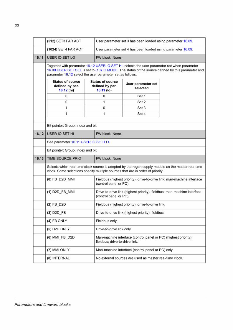
Parameters and firmware blocks
60
(512) SET3 PAR ACT User parameter set 3 has been loaded using parameter 16.09.
(1024) SET4 PAR ACT User parameter set 4 has been loaded using parameter 16.09.
16.11 USER IO SET LO FW block: None
Together with parameter 16.12 USER IO SET HI, selects the user parameter set when parameter 16.09 USER SET SEL is set to (10) IO MODE. The status of the source defined by this parameter and parameter 16.12 select the user parameter set as follows:
Bit pointer: Group, index and bit
16.12 USER IO SET HI FW block: None
See parameter 16.11 USER IO SET LO.
Bit pointer: Group, index and bit
16.13 TIME SOURCE PRIO FW block: None
Selects which real-time clock source is adopted by the regen supply module as the master real-time clock. Some selections specify multiple sources that are in order of priority.
(0) FB_D2D_MMI Fieldbus (highest priority); drive-to-drive link; man-machine interface (control panel or PC).
(1) D2D_FB_MMI Drive-to-drive link (highest priority); fieldbus; man-machine interface (control panel or PC).
(2) FB_D2D Fieldbus (highest priority); drive-to-drive link.
(3) D2D_FB Drive-to-drive link (highest priority); fieldbus.
(4) FB ONLY Fieldbus only.
(5) D2D ONLY Drive-to-drive link only.
(6) MMI_FB_D2D Man-machine interface (control panel or PC) (highest priority); fieldbus; drive-to-drive link.
(7) MMI ONLY Man-machine interface (control panel or PC) only.
(8) INTERNAL No external sources are used as master real-time clock.
Status of source defined by par.
16.12 (hi)
Status of source defined by par.
16.11 (lo)
User parameter set selected
0 0 Set 1
0 1 Set 2
1 0 Set 3
1 1 Set 4

Parameters and firmware blocks
61
Group 17 PANEL DISPLAYSelection of signals for panel display.
1717 PANEL DISPLAY
17.01 SIGNAL1 PARAM FW block: None
Selects the first signal to be displayed on the control panel. The default signal is 1.07 DC-VOLTAGE.
Value pointer: Group and index
17.02 SIGNAL2 PARAM FW block: None
Selects the second signal to be displayed on the control panel. The default signal is 1.04 CURRENT.
Value pointer: Group and index
17.03 SIGNAL3 PARAM FW block: None
Selects the third signal to be displayed on the control panel. The default signal is 1.22 INVERTER POWER.
Value pointer: Group and index
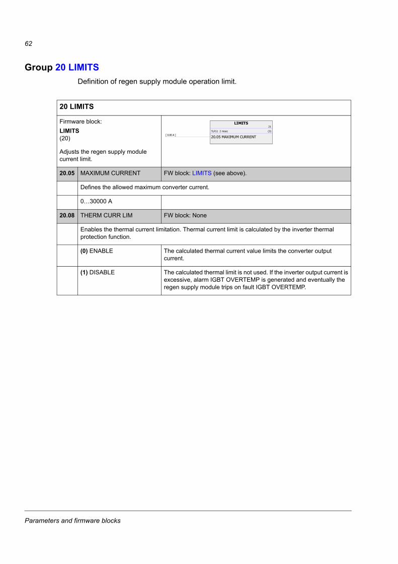
Parameters and firmware blocks
62
Group 20 LIMITSDefinition of regen supply module operation limit.
2020 LIMITS
Firmware block:LIMITS(20)
Adjusts the regen supply module current limit.
20.05 MAXIMUM CURRENT FW block: LIMITS (see above).
Defines the allowed maximum converter current.
0…30000 A
20.08 THERM CURR LIM FW block: None
Enables the thermal current limitation. Thermal current limit is calculated by the inverter thermal protection function.
(0) ENABLE The calculated thermal current value limits the converter output current.
(1) DISABLE The calculated thermal limit is not used. If the inverter output current is excessive, alarm IGBT OVERTEMP is generated and eventually the regen supply module trips on fault IGBT OVERTEMP.
LIMITS21
TLF11 2 msec (3)
20.05 MAXIMUM CURRENT[ 0.00 A ]

Parameters and firmware blocks
63
Group 33 SUPERVISIONConfiguration of signal supervision.
33 SUPERVISION
Firmware block:SUPERVISION(17)
Block outputs located in other parameter groups
6.13 SUPERV STATUS (page 39)
33.01 SUPERV1 FUNC FW block: SUPERVISION (see above)
Selects the mode of supervision 1.
(0) DISABLED Supervision 1 not in use.
(1) LOW When the signal selected by parameter 33.02 SUPERV1 ACT falls below the value of parameter 33.04 SUPERV1 LIM LO, bit 0 of 6.13 SUPERV STATUS is activated. To clear the bit, the signal must exceed the value of parameter 33.03 SUPERV1 LIM HI.
(2) HIGH When the signal selected by parameter 33.02 SUPERV1 ACT exceeds the value of parameter 33.03 SUPERV1 LIM HI, bit 0 of 6.13 SUPERV STATUS is activated. To clear the bit, the signal must exceed the value of parameter 33.04 SUPERV1 LIM LO.
(3) ABS LOW When the absolute value of the signal selected by parameter 33.02 SUPERV1 ACT falls below the value of parameter 33.04 SUPERV1 LIM LO, bit 0 of 6.13 SUPERV STATUS is activated. To clear the bit, the absolute value of the signal must exceed the value of parameter 33.03 SUPERV1 LIM HI.
(4) ABS HIGH When the absolute value of the signal selected by parameter 33.02 SUPERV1 ACT exceeds the value of parameter 33.03 SUPERV1 LIM HI, bit 0 of 6.13 SUPERV STATUS is activated. To clear the bit, the absolute value of the signal must exceed the value of parameter 33.04 SUPERV1 LIM LO.
33.02 SUPERV1 ACT FW block: SUPERVISION (see above)
Selects the signal to be monitored by supervision 1. See parameter 33.01 SUPERV1 FUNC.
Value pointer: Group and index
SUPERVISION35
TLF12 10 msec (4)
33.01 SUPERV1 FUNC(Drive value)
< 33.02 SUPERV1 ACT[ DC-VOLTAGE ]
(1 / 1.07)
33.03 SUPERV1 LIM HI(Drive value)
33.04 SUPERV1 LIM LO(Drive value)
33.05 SUPERV2 FUNC(Drive value)
< 33.06 SUPERV2 ACT[ CURRENT ]
(1 / 1.04)
33.07 SUPERV2 LIM HI(Drive value)
33.08 SUPERV2 LIM LO(Drive value)
33.09 SUPERV3 FUNC(Drive value)
< 33.10 SUPERV3 ACT[ DC-VOLTAGE ]
(1 / 1.07)
33.11 SUPERV3 LIM HI(Drive value)
33.12 SUPERV3 LIM LO(Drive value)
6.14 SUPERV STATUS
Parameters and firmware blocks
64
33.03 SUPERV1 LIM HI FW block: SUPERVISION (see above)
Sets the upper limit for supervision 1. See parameter 33.01 SUPERV1 FUNC.
-32768…32768
33.04 SUPERV1 LIM LO FW block: SUPERVISION (see above)
Sets the lower limit for supervision 1. See parameter 33.01 SUPERV1 FUNC.
-32768…32768
33.05 SUPERV2 FUNC FW block: SUPERVISION (see above)
Selects the mode of supervision 2.
(0) DISABLED Supervision 2 not in use.
(1) LOW When the signal selected by parameter 33.06 SUPERV2 ACT falls below the value of parameter 33.08 SUPERV2 LIM LO, bit 1 of 6.13 SUPERV STATUS is activated. To clear the bit, the signal must exceed the value of parameter 33.07 SUPERV2 LIM HI.
(2) HIGH When the signal selected by parameter 33.06 SUPERV2 ACT exceeds the value of parameter 33.07 SUPERV2 LIM HI, bit 1 of 6.13 SUPERV STATUS is activated. To clear the bit, the signal must exceed the value of parameter 33.08 SUPERV2 LIM LO.
(3) ABS LOW When the absolute value of the signal selected by parameter 33.06 SUPERV2 ACT falls below the value of parameter 33.08 SUPERV2 LIM LO, bit 1 of 6.13 SUPERV STATUS is activated. To clear the bit, the absolute value of the signal must exceed the value of parameter 33.07 SUPERV2 LIM HI.
(4) ABS HIGH When the absolute value of the signal selected by parameter 33.06 SUPERV2 ACT exceeds the value of parameter 33.07 SUPERV2 LIM HI, bit 1 of 6.13 SUPERV STATUS is activated. To clear the bit, the absolute value of the signal must exceed the value of parameter 33.08 SUPERV2 LIM LO.
33.06 SUPERV2 ACT FW block: SUPERVISION (see above)
Selects the signal to be monitored by supervision 2. See parameter 33.05 SUPERV2 FUNC.
Value pointer: Group and index
33.07 SUPERV2 LIM HI FW block: SUPERVISION (see above)
Sets the upper limit for supervision 2. See parameter 33.05 SUPERV2 FUNC.
-32768…32768
33.08 SUPERV2 LIM LO FW block: SUPERVISION (see above)
Sets the lower limit for supervision 2. See parameter 33.05 SUPERV2 FUNC.
-32768…32768

Parameters and firmware blocks
65
33.09 SUPERV3 FUNC FW block: SUPERVISION (see above)
Selects the mode of supervision 3.
(0) DISABLED Supervision 3 not in use.
(1) LOW When the signal selected by parameter 33.10 SUPERV3 ACT falls below the value of parameter 33.12 SUPERV3 LIM LO, bit 2 of 6.13 SUPERV STATUS is activated. To clear the bit, the signal must exceed the value of parameter 33.11 SUPERV3 LIM HI.
(2) HIGH When the signal selected by parameter 33.10 SUPERV3 ACT exceeds the value of parameter 33.11 SUPERV3 LIM HI, bit 2 of 6.13 SUPERV STATUS is activated. To clear the bit, the signal must exceed the value of parameter 33.12 SUPERV3 LIM LO.
(3) ABS LOW When the absolute value of the signal selected by parameter 33.10 SUPERV3 ACT falls below the value of parameter 33.12 SUPERV3 LIM LO, bit 2 of 6.13 SUPERV STATUS is activated. To clear the bit, the absolute value of the signal must exceed the value of parameter 33.11 SUPERV3 LIM HI.
(4) ABS HIGH When the absolute value of the signal selected by parameter 33.10 SUPERV3 ACT exceeds the value of parameter 33.11 SUPERV3 LIM HI, bit 2 of 6.13 SUPERV STATUS is activated. To clear the bit, the absolute value of the signal must exceed the value of parameter 33.12 SUPERV3 LIM LO.
33.10 SUPERV3 ACT FW block: SUPERVISION (see above)
Selects the signal to be monitored by supervision 3. See parameter 33.09 SUPERV3 FUNC.
Value pointer: Group and index
33.11 SUPERV3 LIM HI FW block: SUPERVISION (see above)
Sets the upper limit for supervision 3. See parameter 33.09 SUPERV3 FUNC.
-32768…32768
33.12 SUPERV3 LIM LO FW block: SUPERVISION (see above)
Sets the lower limit for supervision 3. See parameter 33.09 SUPERV3 FUNC.
-32768…32768

Parameters and firmware blocks
66
Group 34 REFERENCE CTRLControl mode selection.
Using the parameters in this group, it is possible to select whether external control location EXT1 or EXT2 is used (either one is active at a time). These parameters also select the control mode (DC VOLTAGE/POWER).
3434 REFERENCE CTRL
Firmware block:REFERENCE CTRL(34)
This block• defines the selection method
between external control locations EXT1 and EXT2
• configures control mode (DC VOLTAGE/POWER) selection
• shows the active operating mode.
Block outputs located in other parameter groups
6.12 OP MODE ACK (page 39)
34.01 EXT1/EXT2 SEL FW block: REFERENCE CTRL (see above)
Selects the source for external control location EXT1/EXT2 selection. 0 = EXT1. 1 = EXT2.
Bit pointer: Group, index and bit
34.03 EXT1 CTRL MODE1 FW block: REFERENCE CTRL (see above)
Selects control mode 1 for external control location EXT1.
(1) DC VOLTAGE
(2) POWER
34.05 EXT2 CTRL MODE1 FW block: REFERENCE CTRL (see above)
Selects control mode for external control location EXT2. For selections, see parameter 34.03 EXT1 CTRL MODE1.
34.07 LOCAL CTRL MODE FW block: REFERENCE CTRL (see above)
Selects the control mode for local control.Note: This parameter cannot be changed while the regen supply module is running.
(1) DC VOLTAGE
(2) POWER
REFERENCE CTRL23
TLF9 250 µsec (4)
< 34.01 EXT1/EXT2 SEL(Drive value)
34.03 EXT1 CTRL MODE1(Drive value)
34.05 EXT2 CTRL MODE1(Drive value)
34.07 LOCAL CTRL MODE(Drive value)
6.12 OP MODE ACK

Parameters and firmware blocks
67
Group 40 CONVERTER CONTROLConverter control settings:
• switching frequency
• voltage reserve
4040 CONVERTER CONTROL
Firmware block:CONVERTER CONTROL(40)
This block defines converter control settings such as• switching frequency• voltage reserve• circulating current elimination• drooping of the DC voltage
controller
Block outputs located in other parameter groups
64.01 CIRC CURR ELIM (page 93)64.02 DC CTRL DROOP EN (page 93)
40.02 SF REF FW block: CONVERTER CONTROL (see above)
Defines the switching frequency of the regen supply module.The higher the switching frequency, the more losses it produces at power stage, the available current magnitude may be reduced.
3/4/5/8/16 kHz Switching frequency.
40.04 VOLTAGE RESERVE FW block: CONVERTER CONTROL (see above)
Defines the minimum allowed DC voltage reference value. If the DC voltage is too low, it is increased internally so that the desired voltage reserve is maintained for control. The default value of 2% is suitable for most cases.Note: The parameter has no effect if circulating current elimination is activated by parameter 64.01.
-4…50 % Minimum allowed voltage reserve.
CONVERTER CONTROL40
TLF11 2 msec (4)
40.02 SF REF(Drive value)
40.04 VOLTAGE RESERVE(Drive value)
64.01 CIRC CURR ELIM(Drive value)
64.02 DC CTRL DROOP EN(Drive value)

Parameters and firmware blocks
68
Group 45 EXT THERM PROTSettings for thermal protection of the regen supply.
4545 EXT THERM PROT
Firmware block:EXT TEMP PROT(45)
Configures overtemperature protection based on external temperature measurement.
Block outputs located in other parameter groups
1.17 EXT TEMP (page 29)
45.01 EXT TEMP PROT FW block: EXT TEMP PROT (see above)
Selects how the regen supply module reacts when overtemperature is detected.
(0) NO No reaction.
(1) ALARM The regen supply module generates warning EXT TEMPERATURE when overtemperature is detected.
(2) FAULT The regen supply module trips on fault EXT OVERTEMP when overtemperature is detected.Note: The warning EXT TEMPERATURE may be generated before fault trip. Warning/fault levels are defined by parameters 45.03 and 45.04, respectively.
45.02 EXT TEMP SOURCE FW block: EXT TEMP PROT (see above)
Selects the signal type and source for temperature supervision. When overtemperature is detected, the regen supply module reacts as defined by parameter 45.01 EXT TEMP PROT.
(0) NONE No temperature measurement selected.
(1) KTY JCU The temperature is supervised using a KTY84 sensor connected to thermistor input TH on the control unit.
(2) PTC JCU The temperature is supervised using 1…3 PTC sensors connected to thermistor input TH on the control unit.
EXT THERM PROT26
TLF12 10 msec (2)
45.01 EXT TEMP PROT(Drive value)
45.02 EXT TEMP SOURCE(Drive value)
45.03 EXT TEMP ALM LIM(Drive value)
45.04 EXT TEMP FLT LIM(Drive value)
1.17 EXT TEMP

Parameters and firmware blocks
69
45.03 EXT TEMP ALM LIM FW block: EXT TEMP PROT (see above)
Defines the alarm limit for the overtemperature protection. Warning EXT TEMPERATURE is generated if temperature measured with KTY84 type sensor exceeds the limit when par. 45.01 EXT TEMP PROT = (1) ALARM/(2) FAULT. The parameter has no effect with PTC type thermistor(s) except when the PTC signal is connected to the JCU (i.e. parameter 45.02 = PTC JCU). In that case, the limit is defined in ohms and the warning is generated when the resistance of the TH input exceeds the limit.
0…10000 °C Overtemperature alarm limit.
45.04 EXT TEMP FLT LIM FW block: EXT TEMP PROT (see above)
Defines the fault limit for the overtemperature protection. Fault EXT OVERTEMP is generated if temperature measured with KTY84 type sensor exceeds the limit and par. 45.01 EXT TEMP PROT = (2) FAULT. The parameter has no effect with PTC type thermistor(s) except when the PTC signal is connected to the JCU (i.e. parameter 45.02 = PTC JCU). In that case, the limit is defined in ohms and the fault is generated when the resistance of the TH input exceeds the limit.
0…10000 °C Overtemperature fault limit.
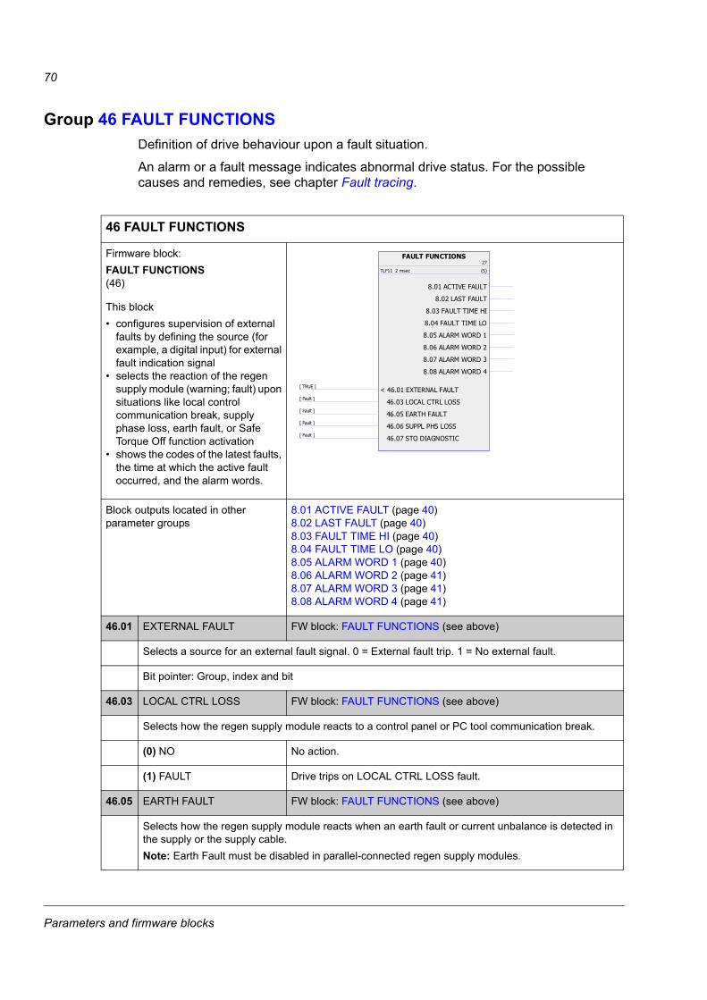
Parameters and firmware blocks
70
Group 46 FAULT FUNCTIONSDefinition of drive behaviour upon a fault situation.
An alarm or a fault message indicates abnormal drive status. For the possible causes and remedies, see chapter Fault tracing.
4646 FAULT FUNCTIONS
Firmware block:FAULT FUNCTIONS(46)
This block• configures supervision of external
faults by defining the source (for example, a digital input) for external fault indication signal
• selects the reaction of the regen supply module (warning; fault) upon situations like local control communication break, supply phase loss, earth fault, or Safe Torque Off function activation
• shows the codes of the latest faults, the time at which the active fault occurred, and the alarm words.
Block outputs located in other parameter groups
8.01 ACTIVE FAULT (page 40)8.02 LAST FAULT (page 40)8.03 FAULT TIME HI (page 40)8.04 FAULT TIME LO (page 40)8.05 ALARM WORD 1 (page 40)8.06 ALARM WORD 2 (page 41)8.07 ALARM WORD 3 (page 41)8.08 ALARM WORD 4 (page 41)
46.01 EXTERNAL FAULT FW block: FAULT FUNCTIONS (see above)
Selects a source for an external fault signal. 0 = External fault trip. 1 = No external fault.
Bit pointer: Group, index and bit
46.03 LOCAL CTRL LOSS FW block: FAULT FUNCTIONS (see above)
Selects how the regen supply module reacts to a control panel or PC tool communication break.
(0) NO No action.
(1) FAULT Drive trips on LOCAL CTRL LOSS fault.
46.05 EARTH FAULT FW block: FAULT FUNCTIONS (see above)
Selects how the regen supply module reacts when an earth fault or current unbalance is detected in the supply or the supply cable.Note: Earth Fault must be disabled in parallel-connected regen supply modules.
FAULT FUNCTIONS27
TLF11 2 msec (5)
< 46.01 EXTERNAL FAULT[ TRUE ]
46.03 LOCAL CTRL LOSS[ Fault ]
46.05 EARTH FAULT[ Fault ]
46.06 SUPPL PHS LOSS[ Fault ]
46.07 STO DIAGNOSTIC[ Fault ]
8.01 ACTIVE FAULT
8.02 LAST FAULT
8.03 FAULT TIME HI
8.04 FAULT TIME LO
8.05 ALARM WORD 1
8.06 ALARM WORD 2
8.07 ALARM WORD 3
8.08 ALARM WORD 4

Parameters and firmware blocks
71
(0) NO No action.
(1) WARNING The regen supply module generates alarm EARTH FAULT.
(2) FAULT The regen supply module trips on EARTH FAULT.
46.06 SUPPL PHS LOSS FW block: FAULT FUNCTIONS (see above)
Selects how the regen supply module reacts when a supply phase loss is detected.Note: Missing supply phase is detected only during synchronization to supply network.
(0) NO No reaction.
(1) FAULT Supply module trips on SUPPLY PHASE fault (default).
46.07 STO DIAGNOSTIC FW block: FAULT FUNCTIONS (see above)
Selects how the regen supply module reacts when the Safe Torque Off function is active while the regen supply module is not modulating. The Safe Torque Off function disables the control voltage of the power semiconductors of the output stage, thus preventing the regen supply module to re-generate power from DC bus to supply network. For Safe Torque Off wiring, see the Hardware Manual.Note: This parameter is only for supervision. The Safe Torque Off function can activate, even when this parameter selection is NO.Note: Fault STO 1 LOST / STO 2 LOST is activated if safety circuit signal 1/2 is lost when the regen supply module is at stopped state and this parameter is set to (2) ALARM or (3) NO.WARNING! The Safe Torque Off function does not prevent power flow from supply network to DC link.
(1) FAULT Supply module trips on SAFE TORQUE OFF fault.
(2) ALARM Supply module generates SAFE TORQUE OFF warning.
(3) NO No reaction.

Parameters and firmware blocks
72
Group 47 VOLTAGE CTRLConfigures charging of the DC-link capacitors.
4747 VOLTAGE CTRL
Firmware block:VOLTAGE CTRL(47)
This block• enables/disables automatic
identification of supply voltage• provides a parameter for manual
definition of supply voltage• shows the supply voltage value
used in charging relay control.
Block outputs located in other parameter groups
1.19 USED SUPPLY VOLT (page 29)
47.03 SUPPLVOLTAUTO-ID FW block: VOLTAGE CTRL (see above)
Enables the auto-identification of the supply voltage.
(0) DISABLE Auto-identification of supply voltage disabled.
(1) ENABLE Auto-identification of supply voltage enabled.
47.04 SUPPLY VOLTAGE FW block: VOLTAGE CTRL (see above)
Defines the nominal supply voltage. Used if auto-identification of the supply voltage is not enabled by parameter 47.03 SUPPLVOLTAUTO-ID.
0…1000 V Nominal supply voltage.
VOLTAGE CTRL28
TLF12 10 msec (1)
47.03 SUPPLVOLTAUTO-ID[ Enable ]
47.04 SUPPLY VOLTAGE[ 400.0 V ]
1.19 USED SUPPLY VOLT

Parameters and firmware blocks
73
Group 48 BRAKE CHOPPERConfiguration of internal brake chopper.
4848 BRAKE CHOPPER
Firmware block:BRAKE CHOPPER(48)
This block configures the brake chopper control and supervision.
48.01 BC ENABLE FW block: BRAKE CHOPPER (see above)
Enables the brake chopper control.Note: Before enabling brake chopper control, ensure the brake resistor is installed. The regen supply module has a built-in brake chopper.
(0) DISABLE Brake chopper control disabled.
(1) ENABLETHERM Enable brake chopper control with resistor overload protection.
(2) ENABLE Enable brake chopper control without resistor overload protection. This setting can be used, for example, if the resistor is equipped with a thermal circuit breaker that is wired to stop the drive if the resistor overheats.
48.02 BC RUN-TIME ENA FW block: BRAKE CHOPPER (see above)
Selects the source for quick run-time brake chopper control.0 = Brake chopper IGBT pulses are cut off.1 = Normal brake chopper IGBT modulation. The overvoltage control is automatically switched off.This parameter can be used to program the chopper control to function only when the drive is operating in generating mode.
Bit pointer: Group, index and bit
48.03 BRTHERMTIMECONST FW block: BRAKE CHOPPER (see above)
Defines the thermal time constant of the brake resistor for overload protection.
0…10000 s Brake resistor thermal time constant.
48.04 BR POWER MAX CNT FW block: BRAKE CHOPPER (see above)
Defines the maximum continuous braking power which will raise the resistor temperature to the maximum allowed value. The value is used in the overload protection.
0…10000 kW Maximum continuous braking power.
BRAKE CHOPPER29
TLF11 2 msec (6)
48.01 BC ENABLE[ Disable ]
< 48.02 BC RUN-TIME ENA[ TRUE ]
48.03 BRTHERMTIMECONST[ 0 s ]
48.04 BR POWER MAX CNT[ 0.0000 kW ]
48.05 R BR[ 0.0000 Ohm ]
48.06 BR TEMP FAULTLIM[ 105 % ]
48.07 BR TEMP ALARMLIM[ 95 % ]

Parameters and firmware blocks
74
48.05 R BR FW block: BRAKE CHOPPER (see above)
Defines the resistance value of the brake resistor. The value is used for brake chopper protection.
0.1…1000 ohm Resistance.
48.06 BR TEMP FAULTLIM FW block: BRAKE CHOPPER (see above)
Selects the fault limit for the brake resistor temperature supervision. The value is given in percent of the temperature the resistor reaches when loaded with the power defined by parameter 48.04 BR POWER MAX CNT.When the limit is exceeded the drive trips on fault BR OVERHEAT.
0…150% Resistor temperature fault limit.
48.07 BR TEMP ALARMLIM FW block: BRAKE CHOPPER (see above)
Selects the alarm limit for the brake resistor temperature supervision. The value is given in percent of the temperature the resistor reaches when loaded with the power defined by parameter 48.04 BR POWER MAX CNT.When limit is exceeded the drive generates alarm BR OVERHEAT.
0…150% Resistor temperature alarm limit.
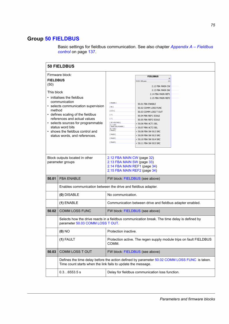
Parameters and firmware blocks
75
Group 50 FIELDBUSBasic settings for fieldbus communication. See also chapter Appendix A – Fieldbus control on page 137.
5050 FIELDBUS
Firmware block:FIELDBUS(50)
This block• initialises the fieldbus
communication• selects communication supervision
method• defines scaling of the fieldbus
references and actual values• selects sources for programmable
status word bits• shows the fieldbus control and
status words, and references.
Block outputs located in other parameter groups
2.12 FBA MAIN CW (page 32)2.13 FBA MAIN SW (page 33)2.14 FBA MAIN REF1 (page 34)2.15 FBA MAIN REF2 (page 34)
50.01 FBA ENABLE FW block: FIELDBUS (see above)
Enables communication between the drive and fieldbus adapter.
(0) DISABLE No communication.
(1) ENABLE Communication between drive and fieldbus adapter enabled.
50.02 COMM LOSS FUNC FW block: FIELDBUS (see above)
Selects how the drive reacts in a fieldbus communication break. The time delay is defined by parameter 50.03 COMM LOSS T OUT.
(0) NO Protection inactive.
(1) FAULT Protection active. The regen supply module trips on fault FIELDBUS COMM.
50.03 COMM LOSS T OUT FW block: FIELDBUS (see above)
Defines the time delay before the action defined by parameter 50.02 COMM LOSS FUNC is taken. Time count starts when the link fails to update the message.
0.3…6553.5 s Delay for fieldbus communication loss function.
FIELDBUS30
TLF10 500 µsec (1)
50.01 FBA ENABLE[ Disable ]
50.02 COMM LOSS FUNC[ No ]
50.03 COMM LOSS T OUT[ 0.3 s ]
50.04 FBA REF1 SCALE[ ? ]
50.05 FBA REF2 SCALE[ ? ]
< 50.06 FBA ACT1 SEL[ DC-VOLTAGE ]
(1 / 1.07)
< 50.07 FBA ACT2 SEL[ REACTIVE POWER ]
(6 / 4.01)
< 50.08 FBA SW B12 SRC[ FALSE ]
< 50.09 FBA SW B13 SRC[ FALSE ]
< 50.10 FBA SW B14 SRC[ FALSE ]
< 50.11 FBA SW B15 SRC[ FALSE ]
2.12 FBA MAIN CW
2.13 FBA MAIN SW
2.14 FBA MAIN REF1
2.15 FBA MAIN REF2

Parameters and firmware blocks
76
50.04 FBA REF1 SCALE FW block: FIELDBUS (see above)
Selects scaling of fieldbus reference FBA REF1. The same scale is also used for actual value FBA ACT1. Defines the correspondence of the internal real value and 16 bit signed integer value used with ABB Drives Profile.
(0) RAW DATA No scaling (i.e. data is transmitted without scaling).
(1) 100 = 1.00 Real value can be given with two decimals as an integer. For example, 10000 = 100.00 [SI unit]. Suitable e.g. for re-active/active powers in value range -327.68…+327.67 [kVAr/kW] according to the value range of signed 16 bit integers.
(2) 10 = 1.0 Real value can be given with one decimal as an integer. For example, 20000 = 2000.0 [SI unit]. Value range -3276.8...+3276.7 is adequate e.g. for DC voltage.
50.05 FBA REF2 SCALE FW block: FIELDBUS (see above)
Selects scaling of fieldbus reference FBA REF2. The same scale is also used for actual value FBA ACT2. Defines the correspondence of the internal real value and 16 bit signed integer value used with ABB Drives Profile.
(0) RAW DATA No scaling (i.e. data is transmitted without scaling).
(1) 100 = 1.00 Real value can be given with two decimals as an integer. For example, 10000 = 100.00 [SI unit]. Suitable e.g. for re-active/active powers in value range -327.68…+327.67 [kVAr/kW] according to the value range of signed 16 bit integers.
(2) 10 = 1.0 Real value can be given with one decimal as an integer. For example, 20000 = 2000.0 [SI unit]. Value range -3276.8...+3276.7 is adequate e.g. for DC voltage.
50.06 FBA ACT1 SEL FW block: FIELDBUS (see above)
Selects the actual value (FBA ACT1), which is sent to the fieldbus corresponding to FBA REF1. Scaling of FBA ACT1 is defined by parameter 50.04 FBA REF1 SCALE.
(1073742087) DC VOLTAGE Signal 1.07 DC-VOLTAGE is sent to the fieldbus as an actual value 1. Select when DC voltage reference is written from the fieldbus as reference 1 i.e. 60.01 DC REF SEL = FBA REF1.
(1073742849) REACT. POWER
Signal 4.01 REACTIVE POWER is sent to the fieldbus as an actual value 1. Select when reactive power reference is written from the fieldbus as reference 1 i.e. 61.01 Q POWER REF SEL = FBA REF1.
(1073742102) ACTIVE POWER
Signal 1.22 INVERTER POWER is sent to the fieldbus as an actual value 1. Select when power reference is written from the fieldbus as reference 1 i.e. 62.01 POW REF SEL = FBA REF1.
50.07 FBA ACT2 SEL FW block: FIELDBUS (see above)
Selects the actual value (FBA ACT2), which is sent to the fieldbus corresponding to FBA REF2. Scaling of FBA ACT2 is defined by parameter 50.05 FBA REF2 SCALE.
(1073742087) DC VOLTAGE Signal 1.07 DC-VOLTAGE is sent to the fieldbus as an actual value 2. Select when DC voltage reference is written from the fieldbus as reference 2, i.e. 60.01 DC REF SEL = FBA REF2.

Parameters and firmware blocks
77
(1073742849) REACT. POWER
Signal 4.01 REACTIVE POWER is sent to the fieldbus as an actual value 2. Select when reactive power reference is written from the fieldbus as reference 2, i.e. 61.01 Q POWER REF SEL = FBA REF2.
(1073742102) ACTIVE POWER
Signal 1.22 INVERTER POWER is sent to the fieldbus as an actual value 2. Select when power reference is written from the fieldbus as reference 2, i.e. 62.01 POW REF SEL = FBA REF2.
50.08 FBA SW B12 SRC FW block: FIELDBUS (see above)
Selects the source for freely programmable fieldbus status word bit 28 (2.13 FBA MAIN SW bit 28 SW B12).
Bit pointer: Group, index and bit
50.09 FBA SW B13 SRC FW block: FIELDBUS (see above)
Selects the source for freely programmable fieldbus status word bit 29 (2.13 FBA MAIN SW bit 29 SW B13).
Bit pointer: Group, index and bit
50.10 FBA SW B14 SRC FW block: FIELDBUS (see above)
Selects the source for freely programmable fieldbus status word bit 30 (2.13 FBA MAIN SW bit 30 SW B14).
Bit pointer: Group, index and bit
50.11 FBA SW B15 SRC FW block: FIELDBUS (see above)
Selects the source for freely programmable fieldbus status word bit 31 (2.13 FBA MAIN SW bit 31 SW B15).
Bit pointer: Group, index and bit

Parameters and firmware blocks
78
Group 51 FBA SETTINGSFurther fieldbus communication configuration. These parameters need to be set only if a fieldbus adapter module is installed. See also Appendix A – Fieldbus control on page 137.
Notes:• This parameter group is presented in the User’s Manual of the fieldbus adapter as
parameter group 1 or A.
• The new settings will take effect when the drive is powered up the next time (before powering off the drive, wait at least 1 minute), or when parameter 51.27 FBA PAR REFRESH is activated.
5151 FBA SETTINGS
51.01 FBA TYPE FW block: None
Displays the type of the connected fieldbus adapter module.
(0) NOT DEFINED Fieldbus adapter module not found (not properly connected, or disabled by parameter 50.01 FBA ENABLE).
(1) PROFIBUS-DP FPBA-xx PROFIBUS-DP adapter module
(32) CANOpen FCAN-xx CANopen adapter module
(37) DEVICENET FDNA-xx DeviceNet adapter module
(128) ETHERNET FENA Ethernet adapter module
(485) RS-485 COMM FSCA RS-485 adapter module
51.02 FBA PAR2 FW block: None
… …. ….
51.26 FBA PAR26 FW block: None
Parameters 51.02…51.26 are adapter module-specific. For more information, see the User’s Manual of the fieldbus adapter module. Note that not all of these parameters are necessarily visible.
51.27 FBA PAR REFRESH FW block: None
Validates any changed adapter module configuration parameter settings. After refreshing, the value reverts automatically to (0) DONE.Note: This parameter cannot be changed while the drive is running.
(0) DONE Refreshing done.
(1) REFRESH Refreshing.
51.28 PAR TABLE VER FW block: None
Displays the parameter table revision of the fieldbus adapter module mapping file stored in the memory of the drive.In format xyz, where x = major revision number; y = minor revision number; z = correction number.

Parameters and firmware blocks
79
51.29 DRIVE TYPE CODE FW block: None
Displays the drive type code of the fieldbus adapter module mapping file stored in the memory of the drive.Example: 530 = ACSM1-204 Regen supply module.
51.30 MAPPING FILE VER FW block: None
Displays the fieldbus adapter module mapping file revision stored in the memory of the drive. In decimal format. Example: 1 = revision 1.
51.31 D2FBA COMM STA FW block: None
Displays the status of the fieldbus adapter module communication.
(0) IDLE Adapter not configured.
(1) EXEC. INIT Adapter initializing.
(2) TIME OUT A timeout has occurred in the communication between the adapter and the drive.
(3) CONFIG ERROR Adapter configuration error – the major or minor revision code of the common program revision in the fieldbus adapter module is not the revision required by the module (see par. 51.32 FBA COMM SW VER), or mapping file upload has failed more than three times.
(4) OFF-LINE Adapter is off-line.
(5) ON-LINE Adapter is on-line.
(6) RESET Adapter is performing a hardware reset.
51.32 FBA COMM SW VER FW block: None
Displays the common program revision of the adapter module.In format axyz, where a = major revision number, xy = minor revision numbers. z = correction letter.Example: 207B = revision 2.07B.
51.33 FBA APPL SW VER FW block: None
Displays the application program revision of the adapter module.In format axyz, where: a = major revision number, xy = minor revision numbers, z = correction letter.Example: 202A = revision 2.02A.

Parameters and firmware blocks
80
Group 52 FBA DATA INThese parameters select the data to be sent by the drive to the fieldbus controller, and need to be set only if a fieldbus adapter module is installed. See also Appendix A – Fieldbus control on page 137.
Notes:• This parameter group is presented in the User’s Manual of the fieldbus adapter as
parameter group 3 or C.
• The new settings will take effect when the drive is powered up the next time (before powering off the drive, wait at least 1 minute), or when parameter 51.27 FBA PAR REFRESH is activated.
• The maximum number of data words is protocol-dependent.
• If the selected data is 32 bits long, two parameters are reserved for the transmission.
5252 FBA DATA IN
52.01 FBA DATA IN1 FW block: None
Selects data to be transferred from the drive to the fieldbus controller.
0 Not in use.
4 Status Word (16 bits).
5 Actual value 1 (16 bits).
6 Actual value 2 (16 bits).
14 Status Word (32 bits).
15 Actual value 1 (32 bits).
16 Actual value 2 (32 bits).
101…9999 Parameter index.
52.02 FBA DATA IN2 FW block: None
… …
52.12 FBA DATA IN12 FW block: None
See 52.01 FBA DATA IN1.
Parameters and firmware blocks
81
Group 53 FBA DATA OUTThese parameters select the data to be sent by the fieldbus controller to the drive, and need to be set only if a fieldbus adapter module is installed. See also Appendix A – Fieldbus control on page 137.
Notes:• This parameter group is presented in the User’s Manual of the fieldbus adapter as
parameter group 2 or B.
• The new settings will take effect when the drive is powered up the next time (before powering off the drive, wait at least 1 minute), or when parameter 51.27 FBA PAR REFRESH is activated.
• The maximum number of data words is protocol-dependent.
• If the selected data is 32 bits long, two parameters are reserved for the transmission.
5353 FBA DATA OUT
53.01 FBA DATA OUT1 FW block: None
Selects data to be transferred from the fieldbus controller to the drive.
0 Not in use.
1 Control Word (16 bits).
2 Reference REF1 (16 bits).
3 Reference REF2 (16 bits).
11 Control Word (32 bits).
12 Reference REF1 (32 bits).
13 Reference REF2 (32 bits).
1001…9999 Parameter index.
53.02 FBA DATA OUT2 FW block: None
…
53.12 FBA DATA OUT12 FW block: None
See 53.01 FBA DATA OUT1.

Parameters and firmware blocks
82
Group 57 D2D COMMUNICATIONDrive-to-drive communication settings. See Appendix B – Drive-to-drive link on page 145.
5757 D2D COMMUNICATION
Firmware block:D2D COMMUNICATION(57)
This block sets up the drive-to-drive communication. It also shows the drive-to-drive control word and the two references received from the link.
Block outputs located in other parameter groups
2.17 D2D MAIN CW (page 34)2.19 D2D REF1 (page 34)2.20 D2D REF2 (page 34)
57.01 LINK MODE FW block: D2D COMMUNICATION (see above)
Activates the drive-to-drive connection.
(0) DISABLED Drive-to-drive connection disabled.
(1) FOLLOWER The regen supply module is a follower on the drive-to-drive link.
(2) MASTER The regen supply module is the master on the drive-to-drive link. Only one regen supply module/drive can be the master at a time.
57.02 COMM LOSS FUNC FW block: D2D COMMUNICATION (see above)
Selects how the regen supply module acts when an erroneous drive-to-drive configuration or a communication break is detected.
(0) NO Supervision inactive.
(1) ALARM The regen supply module generates an alarm.
(2) FAULT The regen supply module trips on a fault.
D2D COMMUNICATION34
TLF10 500 µsec (2)
57.01 LINK MODE[ Disabled ]
57.02 COMM LOSS FUNC[ Alarm ]
57.03 NODE ADDRESS[ 1 ]
57.04 FOLLOWER MASK 1[ 0000 0000 ]
57.05 FOLLOWER MASK 2[ 0000 0000 ]
< 57.06 REF 1 SRC[ DC-VOLTAGE ]
(1 / 1.07)
< 57.07 REF 2 SRC[ DC-VOLTAGE ]
(1 / 1.07)
< 57.08 FOLLOWER CW SRC[ D2D FOLLOWER CW ]
(4 / 2.18)
57.09 KERNEL SYNC MODE[ NoSync ]
57.10 KERNEL SYNC OFFS[ 0.000 ms ]
57.11 REF 1 MSG TYPE[ Broadcast ]
57.12 REF1 MC GROUP[ 0 ]
57.13 NEXT REF1 MC GRP[ 0 ]
57.14 NR REF1 MC GRPS[ 1 ]
2.17 D2D MAIN CW
2.19 D2D REF1
2.20 D2D REF2
Parameters and firmware blocks
83
57.03 NODE ADDRESS FW block: D2D COMMUNICATION (see above)
Sets the node address for a follower regen supply module. Each follower must have a dedicated node address.Note: If the regen supply module is set to be the master on the drive-to-drive link, this parameter has no effect (the master is automatically assigned node address 0).
1…62 Node address.
57.04 FOLLOWER MASK 1 FW block: D2D COMMUNICATION (see above)
On the master regen supply module, selects the followers to be polled. If no response is received from a polled follower, the action selected by parameter 57.02 COMM LOSS FUNC is taken.The least significant bit represents follower with node address 1, while the most significant bit represents follower 31. When a bit is set to 1, the corresponding node address is polled. For example, followers 1 and 2 are polled when this parameter is set to the value of 0x3.
0x00000000…0x7FFFFFFF Follower mask 1.
57.05 FOLLOWER MASK 2 FW block: D2D COMMUNICATION (see above)
On the master regen supply module, selects the followers to be polled. If no response is received from a polled follower, the action selected by parameter 57.02 COMM LOSS FUNC is taken.The least significant bit represents follower with node address 32, while the most significant bit represents follower 62. When a bit is set to 1, the corresponding node address is polled. For example, followers 32 and 33 are polled when this parameter is set to the value of 0x3.
0x00000000…0x7FFFFFFF Follower mask 2.
57.06 REF 1 SRC FW block: D2D COMMUNICATION (see above)
Selects the source of D2D reference 1 sent to the followers. The parameter is effective on the master regen supply module, as well as submasters (57.03 NODE ADDRESS = 57.12 REF1 MC GROUP) in a multicast message chain (see parameter 57.11 REF 1 MSG TYPE).The default value is P.01.07, i.e. 1.07 DC-VOLTAGE.
Value pointer: Group and index.
57.07 REF 2 SRC FW block: D2D COMMUNICATION (see above)
On the master regen supply module, selects the source of D2D reference 2 broadcast to all followers.The default value is P.01.07, i.e. 1.07 DC-VOLTAGE.
Value pointer: Group and index.
57.08 FOLLOWER CW SRC FW block: D2D COMMUNICATION (see above)
Selects the source of the D2D control word sent to the followers. The parameter is effective on the master regen supply module, as well as submasters in a multicast message chain (see parameter 57.11 REF 1 MSG TYPE).The default value is P.02.18, i.e. 2.18 D2D FOLLOWER CW.
Value pointer: Group and index.
57.09 KERNEL SYNC MODE FW block: D2D COMMUNICATION (see above)
Determines which signal the time levels of the regen supply module are synchronised with. An offset can be defined by parameter 57.10 KERNEL SYNC OFFS if desired.

Parameters and firmware blocks
84
(0) NO SYNC No synchronisation.
(1) D2DSYNC If the regen supply module is the master on a drive-to-drive link, it broadcasts a synchronisation signal to the follower(s). If the regen supply module is a follower, it synchronises its firmware time levels to the signal received from the master.
(2) FBSYNC The regen supply module synchronises its firmware time levels to a synchronisation signal received through a fieldbus adapter.
(3) FBTOD2DSYNC If the regen supply module is the master on a drive-to-drive link, it synchronises its firmware time levels to a synchronisation signal received from a fieldbus adapter, and broadcasts the signal on the drive-to-drive link. If the regen supply module is a follower, this setting has no effect.
57.10 KERNEL SYNC OFFS FW block: D2D COMMUNICATION (see above)
Defines an offset between the synchronisation signal received and the time levels of the regen supply module. With a positive value, the regen supply module time levels will lag behind the synchronisation signal; with a negative value, the regen supply module time levels will lead.
-4.999…5.000 ms Synchronisation offset.
57.11 REF 1 MSG TYPE FW block: D2D COMMUNICATION (see above)
By default, in drive-to-drive communication, the master broadcasts the drive-to-drive control word and references 1 and 2 to all followers. This parameter enables multicasting, i.e. sending the drive-to-drive control word and reference 1 to a certain drive/supply module or group of drives/supply modules. The message can then be further relayed to another group of drives/supply modules to form a multicast chain.In the master, as well as any submaster (i.e. follower relaying the message to other followers), the sources for the control word and reference 1 are selected by parameters 57.08 FOLLOWER CW SRC and 57.06 REF 1 SRC respectively.Note: Reference 2 is broadcast to all followers by the masters.For more information, see Appendix B – Drive-to-drive link on page 145.
(0) BROADCAST The control word and reference 1 are sent by the master to all followers. If the master has this setting, the parameter has no effect in the followers.
(1) REF1 MC GRPS The drive-to-drive control word and reference 1 are only sent to the drives/supply modules in the multicast group specified by parameter 57.13 NEXT REF1 MC GRP. This setting can also used in submasters (i.e. followers whose parameters 57.03 and 57.12 have the same value) to form a multicast chain.
57.12 REF1 MC GROUP FW block: D2D COMMUNICATION (see above)
Selects the multicast group the regen supply module belongs to. See parameter 57.11 REF 1 MSG TYPE.
0…62 Multicast group (0 = none).

Parameters and firmware blocks
85
57.13 NEXT REF1 MC GRP FW block: D2D COMMUNICATION (see above)
Specifies the next multicast group of drives/supply modules the multicast message is relayed to. See parameter 57.11 REF 1 MSG TYPE. This parameter is effective only in the master or submasters (i.e. followers whose parameters 57.03 and 57.12 have the same value).
0…62 Next multicast group in message chain.
57.14 NR REF1 MC GRPS FW block: D2D COMMUNICATION (see above)
In the master drive, sets the total number of links (followers or groups of followers) in the multicast message chain. See parameter 57.11 REF 1 MSG TYPE.Notes:• This parameter has no effect if the regen supply module is a follower.• The master counts as a member of the chain if acknowledgement from the last regen supply
module to the master is desired.
1…62 Total number of links in multicast message chain.
57.15 D2D COMM PORT FW block: None
Defines the hardware to which the drive-to-drive link is connected. In special cases (such as harsh operating conditions), the galvanic isolation provided by the RS-485 interface of the FMBA module may make for more robust communication than the standard drive-to-drive connection.
(0) ON-BOARD Connector X5 on the JCU Control Unit is used.
(1) SLOT 1 An FMBA module installed in JCU option slot 1 is used.
(2) SLOT 2 An FMBA module installed in JCU option slot 2 is used.
(3) SLOT 3 An FMBA module installed in JCU option slot 3 is used.

Parameters and firmware blocks
86
Group 60 DC REF SELDC voltage reference settings.
6060 DC REF SEL
Firmware block:DC VOLTAGE CTRL(60)
This block sets up DC voltage reference. It also shows reference values.
Block outputs located in other parameter groups
4.10 DC REF1 (page 35)4.11 DC REF RAMP IN (page 35)4.12 DC REF RAMPED (page 35)4.34 POW REF USED (page 35)
60.01 DC REF SEL FW block: DC VOLTAGE CTRL (see above)
Selects the source of DC voltage reference. The user can select the reference source freely with the value pointer parameter. A pre-defined selection list is provided.The default setting is (0) Internal. In local control mode (with DriveStudio or with control panel) the local reference overrides this selection (see "Local reference" in block diagram).
(0) Internal Zero reference. DC voltage level is determined based on parameter 40.04 VOLTAGE RESERVE.
(1073742341) AI1 Analogue input AI1 (2.05 AI1 SCALED).
(1073742343) AI2 Analogue input AI2 (2.07 AI2 SCALED).
(1073742350) FBA REF1 Fieldbus reference 1 (2.14 FBA MAIN REF1).
(1073742351) FBA REF2 Fieldbus reference 2 (2.15 FBA MAIN REF2).
(1073742355) D2D REF1 Drive-to-drive reference 1 (2.19 D2D REF1).
(1073742356) D2D REF2 Drive-to-drive reference 2 (2.20 D2D REF2).
(1073757186) P.60.02 Parameter 60.02 DC VOLT REF.
60.02 DC VOLT REF FW block: DC VOLTAGE CTRL (see above)
Defines the constant value for DC voltage reference.
0.0…2000 V
DC VOLTAGE CTRL37
TLF9 250 µsec (1)
< 60.01 DC REF SEL(Drive value)
60.02 DC VOLT REF(Drive value)
60.03 DC REF MAX(Drive value)
60.04 DC REF MIN(Drive value)
60.05 DC RAMP UP(Drive value)
60.06 DC RAMP DOWN(Drive value)
4.10 DC REF1
4.11 DC REF RAMP IN
4.12 DC REF RAMPED
4.34 POWER REF USED

Parameters and firmware blocks
87
60.03 DC REF MAX FW block: DC VOLTAGE CTRL (see above)
Defines the maximum allowed DC voltage.
0.0…2000.0 V
60.04 DC REF MIN FW block: DC VOLTAGE CTRL (see above)
Defines the minimum allowed DC voltage.
0.0…2000.0 V
60.05 DC RAMP UP FW block: DC VOLTAGE CTRL (see above)
Defines the DC voltage ramp time in milliseconds as the time required for the DC voltage reference to change by 100 V DC. The value is active when the reference is increasing i.e. changing away from zero.
60.06 DC RAMP DOWN FW block: DC VOLTAGE CTRL (see above)
Defines the DC voltage ramp time in milliseconds as the time required for the DC voltage reference to change by 100 V DC. The value is active when the reference is decreasing i.e. changing towards zero.
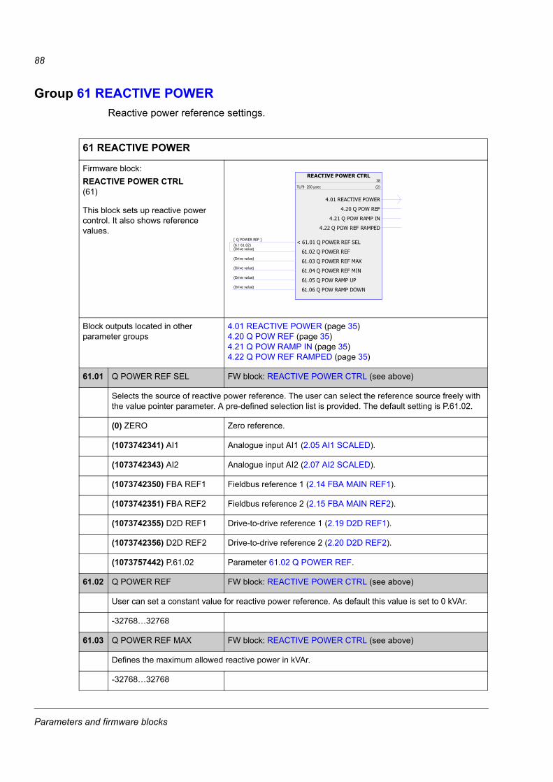
Parameters and firmware blocks
88
Group 61 REACTIVE POWERReactive power reference settings.
6261 REACTIVE POWER
Firmware block:REACTIVE POWER CTRL(61)
This block sets up reactive power control. It also shows reference values.
Block outputs located in other parameter groups
4.01 REACTIVE POWER (page 35)4.20 Q POW REF (page 35)4.21 Q POW RAMP IN (page 35)4.22 Q POW REF RAMPED (page 35)
61.01 Q POWER REF SEL FW block: REACTIVE POWER CTRL (see above)
Selects the source of reactive power reference. The user can select the reference source freely with the value pointer parameter. A pre-defined selection list is provided. The default setting is P.61.02.
(0) ZERO Zero reference.
(1073742341) AI1 Analogue input AI1 (2.05 AI1 SCALED).
(1073742343) AI2 Analogue input AI2 (2.07 AI2 SCALED).
(1073742350) FBA REF1 Fieldbus reference 1 (2.14 FBA MAIN REF1).
(1073742351) FBA REF2 Fieldbus reference 2 (2.15 FBA MAIN REF2).
(1073742355) D2D REF1 Drive-to-drive reference 1 (2.19 D2D REF1).
(1073742356) D2D REF2 Drive-to-drive reference 2 (2.20 D2D REF2).
(1073757442) P.61.02 Parameter 61.02 Q POWER REF.
61.02 Q POWER REF FW block: REACTIVE POWER CTRL (see above)
User can set a constant value for reactive power reference. As default this value is set to 0 kVAr.
-32768…32768
61.03 Q POWER REF MAX FW block: REACTIVE POWER CTRL (see above)
Defines the maximum allowed reactive power in kVAr.
-32768…32768
REACTIVE POWER CTRL38
TLF9 250 µsec (2)
< 61.01 Q POWER REF SEL[ Q POWER REF ]
(6 / 61.02)
61.02 Q POWER REF(Drive value)
61.03 Q POWER REF MAX(Drive value)
61.04 Q POWER REF MIN(Drive value)
61.05 Q POW RAMP UP(Drive value)
61.06 Q POW RAMP DOWN(Drive value)
4.01 REACTIVE POWER
4.20 Q POW REF
4.21 Q POW RAMP IN
4.22 Q POW REF RAMPED

Parameters and firmware blocks
89
61.04 Q POWER REF MIN FW block: REACTIVE POWER CTRL (see above)
Defines the minimum allowed reactive power in kVAr.
-32768…32768 .
61.05 Q POW RAMP UP FW block: REACTIVE POWER CTRL (see above)
Defines the time in milliseconds required for the reactive power reference to change by 1000 kVAr. The value is active when the absolute value of the reference is increasing i.e. the reference is changing away from zero either on the positive side or on the negative side.
0…32768
61.06 Q POW RAMP DOWN FW block: REACTIVE POWER CTRL (see above)
Defines the time in milliseconds required for the reactive power reference to change by 1000 kVAr. The value is active when the absolute value of the reference is decreasing i.e. the reference is changing towards zero either on the positive side or on the negative side.
0…32768

Parameters and firmware blocks
90
Group 62 POWER REFActive power reference settings.
6262 POWER REF
Firmware block:ACTIVE POWER REF(62)
This block sets up active power reference. It also shows reference vales.
Block outputs located in other parameter groups
4.30 POW REF1 (page 35)4.31 POW REF RAMP IN (page 35)4.31 POW REF RAMPED (page 35)
62.01 POW REF SEL FW block: ACTIVE POWER REF (see above)
Selects the source of active power reference. The user can select the reference source freely with the value pointer parameter. A pre-defined selection list is provided. The default setting is P.62.02.
(0) ZERO Zero reference.
(1073742341) AI1 Analogue input AI1 (2.05 AI1 SCALED).
(1073742343) AI2 Analogue input AI2 (2.07 AI2 SCALED).
(1073742350) FBA REF1 Fieldbus reference 1 (2.14 FBA MAIN REF1).
(1073742351) FBA REF2 Fieldbus reference 2 (2.15 FBA MAIN REF2).
(1073742355) D2D REF1 Drive-to-drive reference 1 (2.19 D2D REF1).
(1073742356) D2D REF2 Drive-to-drive reference 2 (2.20 D2D REF2).
(1073757698) P.62.02 Parameter 62.02 POWER REF.
62.02 POWER REF FW block: ACTIVE POWER REF (see above)
You can set a constant value for active power reference of power control mode. By default this value is set to 0 kW.
-32768…32768
62.03 MAXIMUM POW REF FW block: ACTIVE POWER REF (see above)
Defines the maximum allowed active power in kW. This parameter affects both the power control mode and the DC voltage control mode.
-32768…32768
ACTIVE POWER REF39
TLF9 250 µsec (3)
< 62.01 POW REF SEL[ POWER REF ]
(6 / 62.02)
62.02 POWER REF(Drive value)
62.03 MAXIMUM POW REF(Drive value)
62.04 MINIMUM POW REF(Drive value)
62.05 POW RAMP UP(Drive value)
62.06 POW RAMP DOWN(Drive value)
4.30 POW REF1
4.31 POW REF RAMP IN
4.32 POW REF RAMPED

Parameters and firmware blocks
91
62.04 MINIMUM POW REF FW block: ACTIVE POWER REF (see above)
Defines the minimum allowed active power in kW. This parameter affects both the power control mode and the DC voltage control mode.
-32768…32768
62.05 POW RAMP UP FW block: ACTIVE POWER REF (see above)
Defines the time in milliseconds required for the active power reference to change by 1000 kW. The value is active when the absolute value of the reference is increasing i.e. the reference is changing away from zero either on the positive side or on the negative side.
0…32768
62.06 POW RAMP DOWN FW block: ACTIVE POWER REF (see above)
Defines the time in milliseconds required for the active power reference to change by 1000 kW. The value is active when the absolute value of the reference is decreasing i.e. the reference is changing towards zero either on the positive side or on the negative side.
0…32768
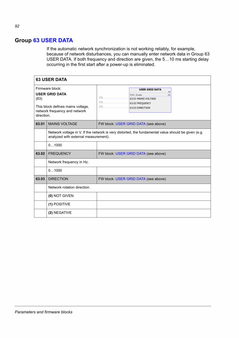
Parameters and firmware blocks
92
Group 63 USER DATAIf the automatic network synchronization is not working reliably, for example, because of network disturbances, you can manually enter network data in Group 63 USER DATA. If both frequency and direction are given, the 5…10 ms starting delay occurring in the first start after a power-up is eliminated.
6263 USER DATA
Firmware block:USER GRID DATA(63)
This block defines mains voltage, network frequency and network direction.
63.01 MAINS VOLTAGE FW block: USER GRID DATA (see above)
Network voltage in V. If the network is very distorted, the fundamental value should be given (e.g. analyzed with external measurement).
0…1000
63.02 FREQUENCY FW block: USER GRID DATA (see above)
Network frequency in Hz.
0…1000
63.03 DIRECTION FW block: USER GRID DATA (see above)
Network rotation direction.
(0) NOT GIVEN
(1) POSITIVE
(2) NEGATIVE
USER GRID DATA42
TLF12 10 msec (5)
63.01 MAINS VOLTAGE[ ? ]
63.02 FREQUENCY[ ? ]
63.03 DIRECTION[ ? ]
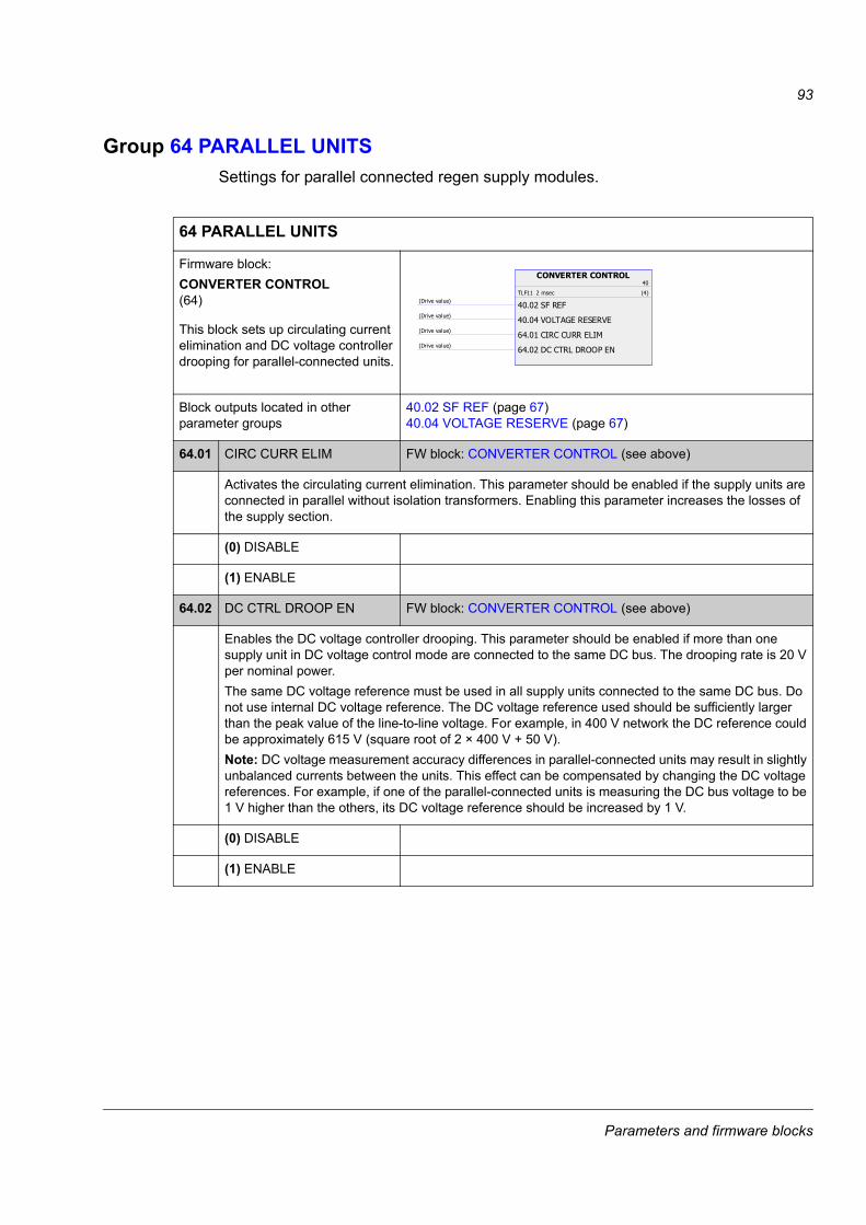
Parameters and firmware blocks
93
Group 64 PARALLEL UNITSSettings for parallel connected regen supply modules.
6264 PARALLEL UNITS
Firmware block:CONVERTER CONTROL(64)
This block sets up circulating current elimination and DC voltage controller drooping for parallel-connected units.
Block outputs located in other parameter groups
40.02 SF REF (page 67)40.04 VOLTAGE RESERVE (page 67)
64.01 CIRC CURR ELIM FW block: CONVERTER CONTROL (see above)
Activates the circulating current elimination. This parameter should be enabled if the supply units are connected in parallel without isolation transformers. Enabling this parameter increases the losses of the supply section.
(0) DISABLE
(1) ENABLE
64.02 DC CTRL DROOP EN FW block: CONVERTER CONTROL (see above)
Enables the DC voltage controller drooping. This parameter should be enabled if more than one supply unit in DC voltage control mode are connected to the same DC bus. The drooping rate is 20 V per nominal power.The same DC voltage reference must be used in all supply units connected to the same DC bus. Do not use internal DC voltage reference. The DC voltage reference used should be sufficiently larger than the peak value of the line-to-line voltage. For example, in 400 V network the DC reference could be approximately 615 V (square root of 2 × 400 V + 50 V). Note: DC voltage measurement accuracy differences in parallel-connected units may result in slightly unbalanced currents between the units. This effect can be compensated by changing the DC voltage references. For example, if one of the parallel-connected units is measuring the DC bus voltage to be 1 V higher than the others, its DC voltage reference should be increased by 1 V.
(0) DISABLE
(1) ENABLE
CONVERTER CONTROL40
TLF11 2 msec (4)
40.02 SF REF(Drive value)
40.04 VOLTAGE RESERVE(Drive value)
64.01 CIRC CURR ELIM(Drive value)
64.02 DC CTRL DROOP EN(Drive value)

Parameters and firmware blocks
94
Group 65 FILTER FAN CTRLRegen filter module fan control settings.
6265 FILTER FAN CTRL
Firmware block:EXT FAN CTRL(65)
This block sets up the ON/OFF control of the cooling fan of the regen filter module:
The fan is always ON when the regen supply module is modulating. In the stopped state, the fan is ON if the current exceeds the limit defined by parameter 65.01 FAN CURRENT LIM. If both of these conditions cease to be met, the fan keeps running for a time defined by parameter 65.02 FAN OFF DELAY to avoid unnecessary stopping and starting of the fan. The fan is controlled via DIO1 by default (see parameters 12.01 DIO1 CONF and 12.04 DIO1 OUT PTR).
Block outputs located in other parameter groups 4.08 EXT FAN COMMAND (page 35)
65.01 FAN CURRENT LIM FW block: EXT FAN CTRL (see above)
Fan current limit.
0.0…1000.0%
65.02 FAN OFF DELAY FW block: EXT FAN CTRL (see above)
Fan minimum run time.
0…42949672 s
OR tModulating
a
b
a>ba=ba<b
01.05 CURRENT PERC
65.01 FAN CURRENT LIM 65.02 FAN OFF DELAY
4.08 EXT FAN COMMAND
TRUE = FAN ON
FALSE = FAN OFF
EXT FAN CTRL41
TLF12 10 msec (3)
65.01 FAN CURRENT LIM(Drive value)
65.02 FAN OFF DELAY(Drive value)
4.08 EXT FAN COMMAND
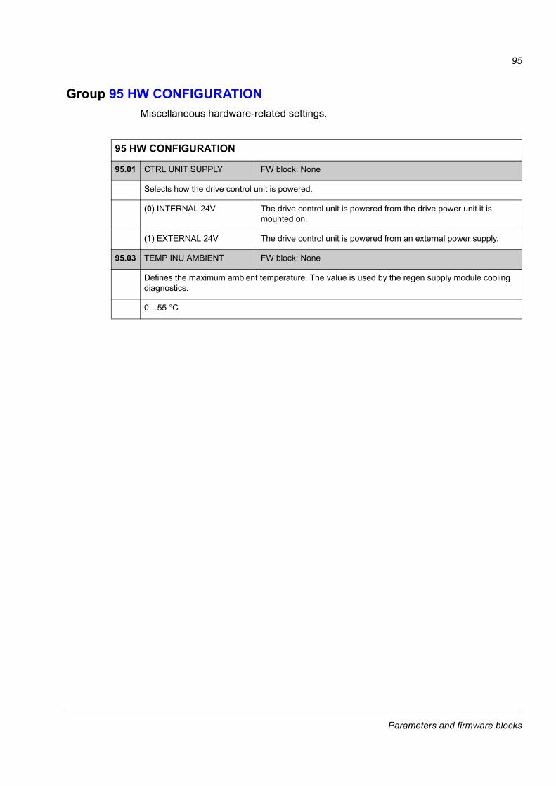
Parameters and firmware blocks
95
Group 95 HW CONFIGURATIONMiscellaneous hardware-related settings.
9595 HW CONFIGURATION
95.01 CTRL UNIT SUPPLY FW block: None
Selects how the drive control unit is powered.
(0) INTERNAL 24V The drive control unit is powered from the drive power unit it is mounted on.
(1) EXTERNAL 24V The drive control unit is powered from an external power supply.
95.03 TEMP INU AMBIENT FW block: None
Defines the maximum ambient temperature. The value is used by the regen supply module cooling diagnostics.
0…55 °C

Parameters and firmware blocks
96
Group 99 START-UP DATAStart-up settings: language and ID-run mode.
9999 START-UP DATA
99.01 LANGUAGE FW block: None
Selects the language.
(2057) ENGLISH English.
(1029) CZECH Czech.
(1030) DANSK Danish.
(1031) DEUTSCH German.
(1034) ESPAÑOL Spanish.
(1035) SUOMI Finnish.
(1036) FRANÇAIS French.
(1038) MAGYAR Hungarian.
(1040) ITALIANO Italian.
(1041) JAPANESE Japanese.
(1042) KOREAN Korean.
(1043) NEDERLANDS Dutch.
(1045) POLSKI Polish.
(1049) RUSSKI Russian.
(1053) SVENSKA Swedish.
(1055) TÜRKÇE Turkish.
(2052) CHINESE Chinese.
(2070) PORTUGUES Portuguese.
99.13 IDRUN MODE FW block: None
ID-run is a way to get values for the user data parameters 63.01…63.03.
(0) NOT ACTIVE No network ID run is requested.
(1) NORMAL Initiate ID-run. Supply section must be started for ID-run to start.
(2) CLEAR RESULT Clears parameters 63.01…63.03. Cancels initiated ID-run. The next start is in automatic mode. All parameters are identified which causes a 5…10 ms start delay.
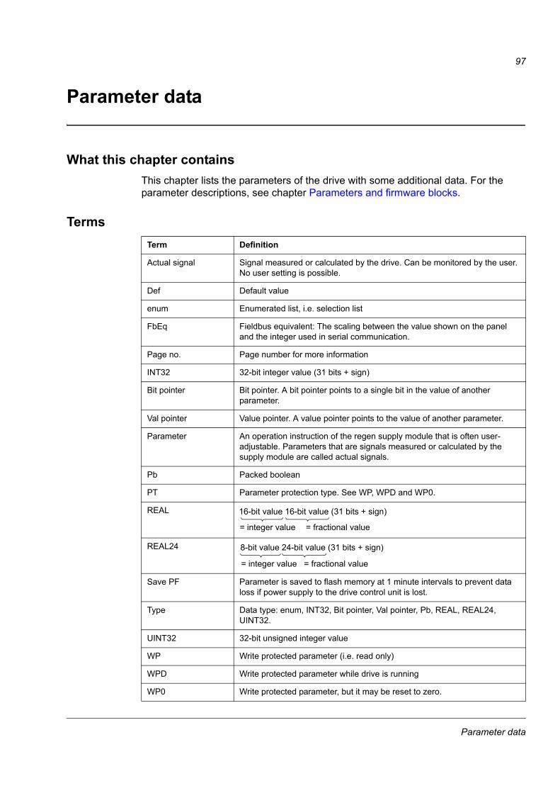
Parameter data
97
Parameter data
What this chapter containsThis chapter lists the parameters of the drive with some additional data. For the parameter descriptions, see chapter Parameters and firmware blocks.
TermsTerm Definition
Actual signal Signal measured or calculated by the drive. Can be monitored by the user. No user setting is possible.
Def Default value
enum Enumerated list, i.e. selection list
FbEq Fieldbus equivalent: The scaling between the value shown on the panel and the integer used in serial communication.
Page no. Page number for more information
INT32 32-bit integer value (31 bits + sign)
Bit pointer Bit pointer. A bit pointer points to a single bit in the value of another parameter.
Val pointer Value pointer. A value pointer points to the value of another parameter.
Parameter An operation instruction of the regen supply module that is often user-adjustable. Parameters that are signals measured or calculated by the supply module are called actual signals.
Pb Packed boolean
PT Parameter protection type. See WP, WPD and WP0.
REAL
REAL24
Save PF Parameter is saved to flash memory at 1 minute intervals to prevent data loss if power supply to the drive control unit is lost.
Type Data type: enum, INT32, Bit pointer, Val pointer, Pb, REAL, REAL24, UINT32.
UINT32 32-bit unsigned integer value
WP Write protected parameter (i.e. read only)
WPD Write protected parameter while drive is running
WP0 Write protected parameter, but it may be reset to zero.
16-bit value 16-bit value (31 bits + sign)
= integer value = fractional value
8-bit value 24-bit value (31 bits + sign)
= integer value = fractional value

Parameter data
98
Fieldbus equivalentSerial communication data between fieldbus adapter and drive is transferred in integer format. Thus the drive actual and reference signal values must be scaled to 16/32-bit integer values. Fieldbus equivalent defines the scaling between the signal value and the integer used in serial communication.
All the read and sent values are limited to 16/32 bits.
Example: If 20.05 MAXIMUM CURRENT is set from external control system, an integer value of 100 corresponds to 1 A.
Fieldbus addressesFor FPBA-01 Profibus Adapter, FDNA-01 DeviceNet Adapter and FCAN-01 CANopen Adapter, see the User’s Manual of the fieldbus adapter module.
Pointer parameter format in fieldbus communicationValue and bit pointer parameters are transferred between the fieldbus adapter and drive as 32-bit integer values.
32-bit integer value pointersWhen value pointer parameter is connected to the value of another parameter or signal, the format is as follows:
When value pointer parameter is connected to an application program, the format is as follows:
Note: Value pointer parameters which are connected to an application program cannot be set via fieldbus (i.e. read access only).
Bit
30…31 16…29 8…15 0…7
Name Source type Group Index
Value 1 - 1…255 1…255
Description Value pointer is connected to
parameter/signal.
- Group of source parameter
Index of source parameter
Bit
30…31 24…29 0…23
Name Source type Not in use Address
Value 2 - 0…223
Description Value pointer is connected to application
program.
- Relative address of application program
variable
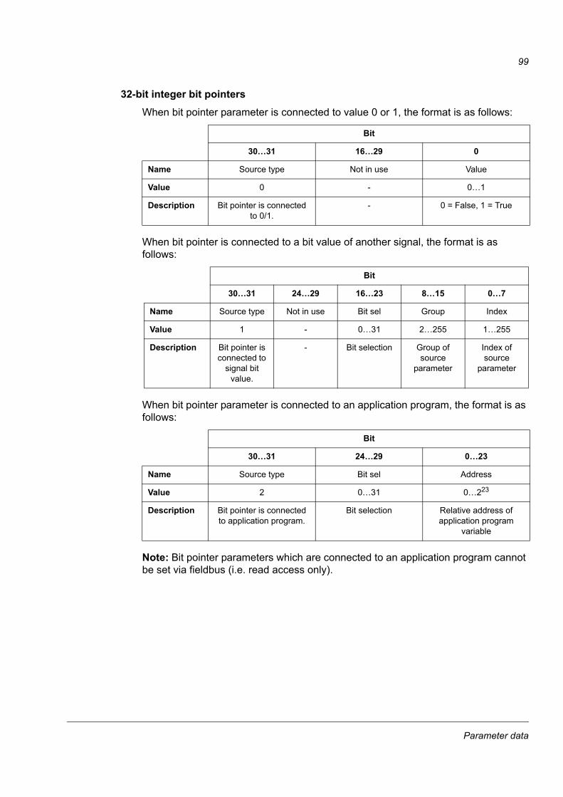
Parameter data
99
32-bit integer bit pointersWhen bit pointer parameter is connected to value 0 or 1, the format is as follows:
When bit pointer is connected to a bit value of another signal, the format is as follows:
When bit pointer parameter is connected to an application program, the format is as follows:
Note: Bit pointer parameters which are connected to an application program cannot be set via fieldbus (i.e. read access only).
Bit
30…31 16…29 0
Name Source type Not in use Value
Value 0 - 0…1
Description Bit pointer is connected to 0/1.
- 0 = False, 1 = True
Bit
30…31 24…29 16…23 8…15 0…7
Name Source type Not in use Bit sel Group Index
Value 1 - 0…31 2…255 1…255
Description Bit pointer is connected to
signal bit value.
- Bit selection Group of source
parameter
Index of source
parameter
Bit
30…31 24…29 0…23
Name Source type Bit sel Address
Value 2 0…31 0…223
Description Bit pointer is connected to application program.
Bit selection Relative address of application program
variable
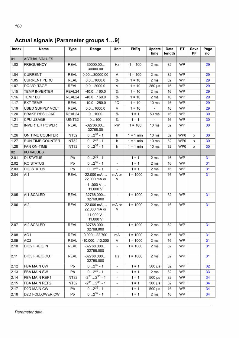
Parameter data
100
Actual signals (Parameter groups 1…9)Index Name Type Range Unit FbEq Update
timeData
lengthPT Save
PFPage no.
01 ACTUAL VALUES1.03 FREQUENCY REAL -30000.00…
30000.00Hz 1 = 100 2 ms 32 WP 29
1.04 CURRENT REAL 0.00…30000.00 A 1 = 100 2 ms 32 WP 291.05 CURRENT PERC REAL 0.0…1000.0 % 1 = 10 2 ms 32 WP 291.07 DC-VOLTAGE REAL 0.0…2000.0 V 1 = 10 250 µs 16 WP 291.15 TEMP INVERTER REAL24 -40.0…160.0 % 1 = 10 2 ms 16 WP 291.16 TEMP BC REAL24 -40.0…160.0 % 1 = 10 2 ms 16 WP 291.17 EXT TEMP REAL -10.0…250.0 °C 1 = 10 10 ms 16 WP 291.19 USED SUPPLY VOLT REAL 0.0…1000.0 V 1 = 10 - 16 WP 291.20 BRAKE RES LOAD REAL24 0…1000 % 1 = 1 50 ms 16 WP 301.21 CPU USAGE UINT32 0…100 % 1 = 1 - 16 WP 301.22 INVERTER POWER REAL -32786.00…
32768.00kW 1 = 100 10 ms 32 WP 30
1.26 ON TIME COUNTER INT32 0…231 - 1 h 1 = 1 min 10 ms 32 WP0 x 301.27 RUN TIME COUNTER INT32 0…231 - 1 h 1 = 1 min 10 ms 32 WP0 x 301.28 FAN ON-TIME INT32 0…231 - 1 h 1 = 1 min 10 ms 32 WP0 x 3002 I/O VALUES2.01 DI STATUS Pb 0…232 - 1 - 1 = 1 2 ms 16 WP 312.02 RO STATUS Pb 0…232 - 1 - 1 = 1 2 ms 16 WP 312.03 DIO STATUS Pb 0…232 - 1 - 1 = 1 2 ms 16 WP 312.04 AI1 REAL -22.000 mA …
22.000 mA or -11.000 V …
11.000 V
mA or V
1 = 1000 2 ms 16 WP 31
2.05 AI1 SCALED REAL -32768.000…32768.000
- 1 = 1000 2 ms 32 WP 31
2.06 AI2 REAL -22.000 mA … 22.000 mA or -11.000 V…
11.000 V
mA or V
1 = 1000 2 ms 16 WP 31
2.07 AI2 SCALED REAL -32768.000…32768.000
- 1 = 1000 2 ms 32 WP 31
2.08 AO1 REAL 0.000…22.700 mA 1 = 1000 2 ms 16 WP 312.09 AO2 REAL -10.000…10.000 V 1 = 1000 2 ms 16 WP 312.10 DIO2 FREQ IN REAL -32768.000…
32768.000- 1 = 1000 2 ms 32 WP 31
2.11 DIO3 FREQ OUT REAL -32768.000…32768.000
Hz 1 = 1000 2 ms 32 WP 31
2.12 FBA MAIN CW Pb 0…232 - 1 - 1 = 1 500 µs 32 WP 322.13 FBA MAIN SW Pb 0…232 - 1 - 1 = 1 2 ms 32 WP 332.14 FBA MAIN REF1 INT32 -231…231 - 1 - 1 = 1 500 µs 32 WP 342.15 FBA MAIN REF2 INT32 -231…231 - 1 - 1 = 1 500 µs 32 WP 342.17 D2D MAIN CW Pb 0…232 - 1 - 1 = 1 500 µs 16 WP 342.18 D2D FOLLOWER CW Pb 0…232 - 1 - 1 = 1 2 ms 16 WP 34
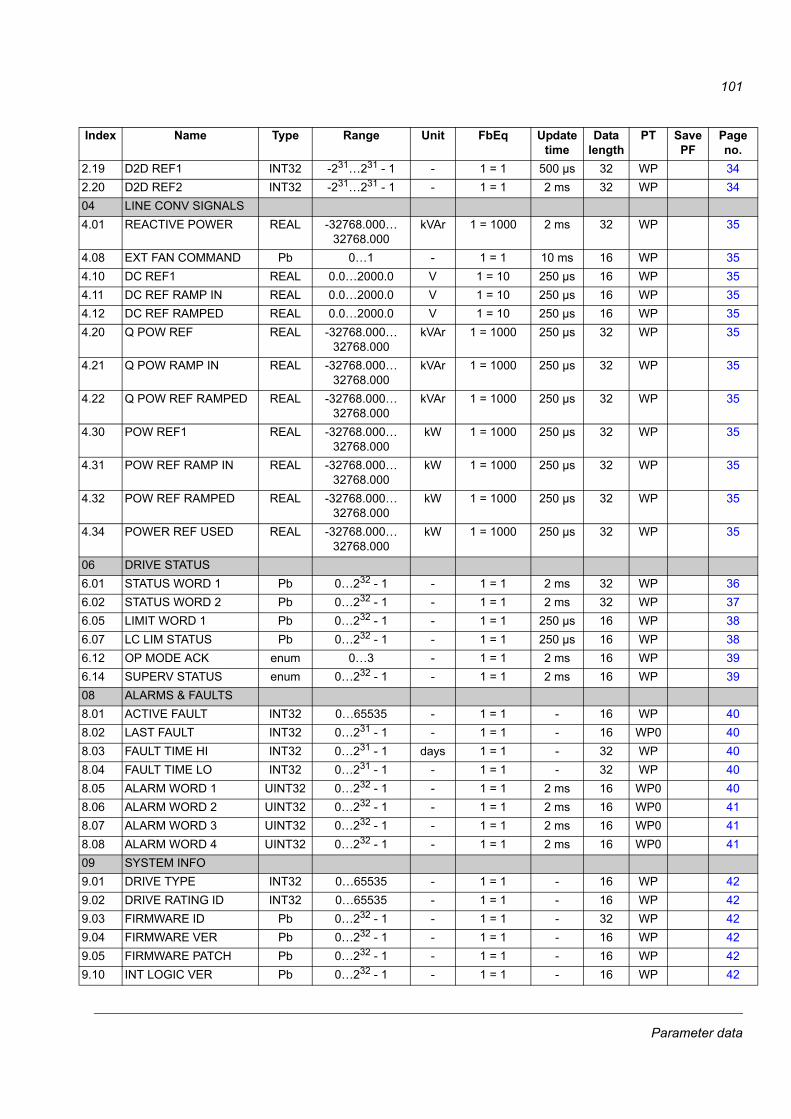
Parameter data
101
2.19 D2D REF1 INT32 -231…231 - 1 - 1 = 1 500 µs 32 WP 342.20 D2D REF2 INT32 -231…231 - 1 - 1 = 1 2 ms 32 WP 3404 LINE CONV SIGNALS4.01 REACTIVE POWER REAL -32768.000…
32768.000kVAr 1 = 1000 2 ms 32 WP 35
4.08 EXT FAN COMMAND Pb 0…1 - 1 = 1 10 ms 16 WP 354.10 DC REF1 REAL 0.0…2000.0 V 1 = 10 250 µs 16 WP 354.11 DC REF RAMP IN REAL 0.0…2000.0 V 1 = 10 250 µs 16 WP 354.12 DC REF RAMPED REAL 0.0…2000.0 V 1 = 10 250 µs 16 WP 354.20 Q POW REF REAL -32768.000…
32768.000kVAr 1 = 1000 250 µs 32 WP 35
4.21 Q POW RAMP IN REAL -32768.000…32768.000
kVAr 1 = 1000 250 µs 32 WP 35
4.22 Q POW REF RAMPED REAL -32768.000…32768.000
kVAr 1 = 1000 250 µs 32 WP 35
4.30 POW REF1 REAL -32768.000…32768.000
kW 1 = 1000 250 µs 32 WP 35
4.31 POW REF RAMP IN REAL -32768.000…32768.000
kW 1 = 1000 250 µs 32 WP 35
4.32 POW REF RAMPED REAL -32768.000…32768.000
kW 1 = 1000 250 µs 32 WP 35
4.34 POWER REF USED REAL -32768.000…32768.000
kW 1 = 1000 250 µs 32 WP 35
06 DRIVE STATUS6.01 STATUS WORD 1 Pb 0…232 - 1 - 1 = 1 2 ms 32 WP 366.02 STATUS WORD 2 Pb 0…232 - 1 - 1 = 1 2 ms 32 WP 376.05 LIMIT WORD 1 Pb 0…232 - 1 - 1 = 1 250 µs 16 WP 386.07 LC LIM STATUS Pb 0…232 - 1 - 1 = 1 250 µs 16 WP 386.12 OP MODE ACK enum 0…3 - 1 = 1 2 ms 16 WP 396.14 SUPERV STATUS enum 0…232 - 1 - 1 = 1 2 ms 16 WP 3908 ALARMS & FAULTS8.01 ACTIVE FAULT INT32 0…65535 - 1 = 1 - 16 WP 408.02 LAST FAULT INT32 0…231 - 1 - 1 = 1 - 16 WP0 408.03 FAULT TIME HI INT32 0…231 - 1 days 1 = 1 - 32 WP 408.04 FAULT TIME LO INT32 0…231 - 1 - 1 = 1 - 32 WP 408.05 ALARM WORD 1 UINT32 0…232 - 1 - 1 = 1 2 ms 16 WP0 408.06 ALARM WORD 2 UINT32 0…232 - 1 - 1 = 1 2 ms 16 WP0 418.07 ALARM WORD 3 UINT32 0…232 - 1 - 1 = 1 2 ms 16 WP0 418.08 ALARM WORD 4 UINT32 0…232 - 1 - 1 = 1 2 ms 16 WP0 4109 SYSTEM INFO9.01 DRIVE TYPE INT32 0…65535 - 1 = 1 - 16 WP 429.02 DRIVE RATING ID INT32 0…65535 - 1 = 1 - 16 WP 429.03 FIRMWARE ID Pb 0…232 - 1 - 1 = 1 - 32 WP 429.04 FIRMWARE VER Pb 0…232 - 1 - 1 = 1 - 16 WP 429.05 FIRMWARE PATCH Pb 0…232 - 1 - 1 = 1 - 16 WP 429.10 INT LOGIC VER Pb 0…232 - 1 - 1 = 1 - 16 WP 42
Index Name Type Range Unit FbEq Update time
Data length
PT Save PF
Page no.

Parameter data
102
9.20 OPTION SLOT 1 INT32 0…24 - 1 = 1 - 16 WP 429.21 OPTION SLOT 2 INT32 0…24 - 1 = 1 - 16 WP 429.22 OPTION SLOT 3 INT32 0…23 - 1 = 1 - 16 WP 42
Index Name Type Range Unit FbEq Update time
Data length
PT Save PF
Page no.

Parameter data
103
Parameter groups 10…99Index Parameter Type Range Unit FbEq Update
timeData len.
Def PT Save PF
Page no.
10 START/STOP10.01 EXT1 START FUNC enum 0…4 - 1 = 1 2 ms 16 1 WPD 4310.02 EXT1 START IN1 Bit pointer 0…232 - 1 - 1 = 1 2 ms 32 C.True WPD 4410.03 EXT1 START IN2 Bit pointer 0…232 - 1 - 1 = 1 2 ms 32 C.False WPD 4410.04 EXT2 START FUNC enum 0…4 - 1 = 1 2 ms 16 1 WPD 4410.05 EXT2 START IN1 Bit pointer 0…232 - 1 - 1 = 1 2 ms 32 P.02.01.00 WPD 4510.06 EXT2 START IN2 Bit pointer 0…232 - 1 - 1 = 1 2 ms 32 C.False WPD 4510.08 FAULT RESET SEL Bit pointer 0…232 - 1 - 1 = 1 2 ms 32 P.02.01.02 4510.09 RUN ENABLE Bit pointer 0…232 - 1 - 1 = 1 2 ms 32 C.True WPD 4510.12 START INHIBIT enum 0…1 - 1 = 1 2 ms 32 0 4510.13 FB CW USED Val pointer 0…232 - 1 - 1 = 1 2 ms 32 P.02.12 WPD 4510.16 D2D CW USED Val pointer 0…232 - 1 - 1 = 1 2 ms 32 P.02.17 4610.17 START ENABLE Bit pointer 0…232 - 1 - 1 = 1 2 ms 32 C.True WPD 4610.18 FORCE STOP Bit pointer 0…232 - 1 - 1 = 1 2 ms 32 P.02.01.03 WPD12 DIGITAL IO12.01 DIO1 CONF enum 0…1 - 1 = 1 10 ms 16 0 4712.02 DIO2 CONF enum 0…2 - 1 = 1 10 ms 16 0 4812.03 DIO3 CONF enum 0…3 - 1 = 1 10 ms 16 0 4812.04 DIO1 OUT PTR Bit pointer 0…232 - 1 - 1 = 1 2 ms 32 P.04.08.00 4812.05 DIO2 OUT PTR Bit pointer 0…232 - 1 - 1 = 1 2 ms 32 P.06.02.03 4812.06 DIO3 OUT PTR Bit pointer 0…232 - 1 - 1 = 1 2 ms 32 P.06.01.10 4812.07 DIO3 F OUT PTR Val pointer 0…232 - 1 - 1 = 1 2 ms 32 P.01.07 4812.08 DIO3 F MAX REAL 3…32768 Hz 1 = 1 10 ms 16 1000 4812.09 DIO3 F MIN REAL 3…32768 Hz 1 = 1 10 ms 16 3 4912.10 DIO3 F MAX SCALE REAL 0…32768 - 1 = 1 10 ms 16 1500 4912.11 DIO3 F MIN SCALE REAL 0…32768 - 1 = 1 10 ms 16 0 4912.12 RO1 OUT PTR Bit pointer 0…232 - 1 - 1 = 1 2 ms 32 P.02.01.00 4912.13 DI INVERT MASK UINT32 0…232 - 1 - 1 = 1 2 ms 16 0 5012.14 DIO2 F MAX REAL 3…32768 Hz 1 = 1 10 ms 16 1000 5012.15 DIO2 F MIN REAL 3…32768 Hz 1 = 1 10 ms 16 3 5012.16 DIO2 F MAX SCALE REAL -32768…
32768- 1 = 1 10 ms 16 1500 50
12.17 DIO2 F MIN SCALE REAL -32768… 32768
- 1 = 1 10 ms 16 0 50
13 ANALOGUE INPUTS13.01 AI1 FILT TIME REAL 0.000…
30.000s 1 = 1000 10 ms 16 0 51
13.02 AI1 MAX REAL -22.000…22.000
mA 1 = 1000 10 ms 16 10.000 51
13.03 AI1 MIN REAL -22.000…22.000
mA 1 = 1000 10 ms 16 -10.000 52
13.04 AI1 MAX SCALE REAL -32768.000…32768.000
- 1 = 1000 10 ms 32 1500.000 52

Parameter data
104
13.05 AI1 MIN SCALE REAL -32768.000…32768.000
- 1 = 1000 10 ms 32 -1500.000 52
13.06 AI2 FILT TIME REAL 0.000…30.000 s 1 = 1000 10 ms 16 0 5213.07 AI2 MAX REAL -22.000…
22.000mA 1 = 1000 10 ms 16 10.000 52
13.08 AI2 MIN REAL -22.000…22.000
mA 1 = 1000 10 ms 16 -10.000 53
13.09 AI2 MAX SCALE REAL -32768.000…32768.000
- 1 = 1000 10 ms 32 100.000 53
13.10 AI2 MIN SCALE REAL -32768.000…32768.000
- 1 = 1000 10 ms 32 -100.000 53
13.11 AITUNE enum 0…4 - 1 = 1 10 ms 16 - 5313.12 AI SUPERVISION enum 0…1 - 1 = 1 2 ms 16 0 5413.13 AI SUPERVIS ACT Pb 0…232 - 1 - 1 = 1 2 ms 16 0 5415 ANALOGUE
OUTPUTS15.01 AO1 PTR Val pointer 0…232 - 1 - 1 = 1 2 ms 32 P.01.05 5515.02 AO1 FILT TIME REAL 0.000…30.000 s 1 = 1000 10 ms 16 0.100 5515.03 AO1 MAX REAL 0.000…22.700 mA 1 = 1000 10 ms 16 20.000 5515.04 AO1 MIN REAL 0.000…22.700 mA 1 = 1000 10 ms 16 4.000 5615.05 AO1 MAX SCALE REAL -32768.000…
32767.000- 1 = 1000 10 ms 32 100.000 56
15.06 AO1 MIN SCALE REAL -32768.000…32767.000
- 1 = 1000 10 ms 32 0.000 56
15.07 AO2 PTR Val pointer 0…232 - 1 - 1 = 1 2 ms 32 P.01.07 5615.08 AO2 FILT TIME REAL 0.000…30.000 s 1 = 1000 10 ms 16 0.100 5615.09 AO2 MAX REAL -10.000…
10.000V 1 = 1000 10 ms 16 10.000 57
15.10 AO2 MIN REAL -10.000…10.000
V 1 = 1000 10 ms 16 -10.000 57
15.11 AO2 MAX SCALE REAL -32768.000…32767.000
- 1 = 1000 10 ms 32 100.000 57
15.12 AO2 MIN SCALE REAL -32768.000…32767.000
- 1 = 1000 10 ms 32 -100.000 57
16 SYSTEM16.01 LOCAL LOCK Bit pointer 0…232 - 1 - 1 = 1 2 ms 32 C.False 5816.02 PARAMETER LOCK enum 0…2 - 1 = 1 2 ms 32 1 5816.03 PASS CODE UINT32 0…231 -1 - 1 = 1 - 32 0 5816.04 PARAM RESTORE enum 0…2 - 1 = 1 - 32 0 WPD 5816.07 PARAM SAVE enum 0…1 - 1 = 1 - 32 0 5816.09 USER SET SEL enum 1…10 - 1 = 1 - 32 1 WPD 5916.10 USER SET LOG Pb 0…232 - 1 - 1 = 1 - 32 0 WP 5916.11 USER IO SEL LO Bit pointer 0…232 - 1 - 1 = 1 - 32 C.False 6016.12 USER IO SEL HI Bit pointer 0…232 - 1 - 1 = 1 - 32 C.False 6016.13 TIME SOURCE PRIO enum 0…8 - 1 = 1 - 16 0 60
Index Parameter Type Range Unit FbEq Update time
Data len.
Def PT Save PF
Page no.
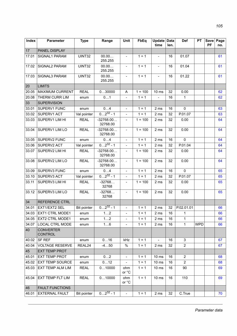
Parameter data
105
17 PANEL DISPLAY17.01 SIGNAL1 PARAM UINT32 00.00…
255.255- 1 = 1 - 16 01.07 61
17.02 SIGNAL2 PARAM UINT32 00.00…255.255
- 1 = 1 - 16 01.04 61
17.03 SIGNAL3 PARAM UINT32 00.00…255.255
- 1 = 1 - 16 01.22 61
20 LIMITS20.05 MAXIMUM CURRENT REAL 0…30000 A 1 = 100 10 ms 32 0.00 6220.08 THERM CURR LIM enum 0…1 - 1 = 1 - 16 1 6233 SUPERVISION33.01 SUPERV1 FUNC enum 0…4 - 1 = 1 2 ms 16 0 6333.02 SUPERV1 ACT Val pointer 0…232 - 1 - 1 = 1 2 ms 32 P.01.07 6333.03 SUPERV1 LIM HI REAL -32768.00…
32768.00- 1 = 100 2 ms 32 0.00 64
33.04 SUPERV1 LIM LO REAL -32768.00… 32768.00
- 1 = 100 2 ms 32 0.00 64
33.05 SUPERV2 FUNC enum 0…4 - 1 = 1 2 ms 16 0 6433.06 SUPERV2 ACT Val pointer 0…232 - 1 - 1 = 1 2 ms 32 P.01.04 6433.07 SUPERV2 LIM HI REAL -32768.00…
32768.00- 1 = 100 2 ms 32 0.00 64
33.08 SUPERV2 LIM LO REAL -32768.00… 32768.00
- 1 = 100 2 ms 32 0.00 64
33.09 SUPERV3 FUNC enum 0…4 - 1 = 1 2 ms 16 0 6533.10 SUPERV3 ACT Val pointer 0…232 - 1 - 1 = 1 2 ms 32 P.01.07 6533.11 SUPERV3 LIM HI REAL -32768…
32768- 1 = 100 2 ms 32 0.00 65
33.12 SUPERV3 LIM LO REAL -32768… 32768
- 1 = 100 2 ms 32 0.00 65
34 REFERENCE CTRL34.01 EXT1/EXT2 SEL Bit pointer 0…232 - 1 - 1 = 1 2 ms 32 P.02.01.01 6634.03 EXT1 CTRL MODE1 enum 1…2 - 1 = 1 2 ms 16 1 6634.05 EXT2 CTRL MODE1 enum 1…2 - 1 = 1 2 ms 16 1 6634.07 LOCAL CTRL MODE enum 1…6 - 1 = 1 2 ms 16 1 WPD 6640 CONVERTER
CONTROL40.02 SF REF enum 0…16 kHz 1 = 1 - 16 3 6740.04 VOLTAGE RESERVE REAL24 -4…50 % 1 = 1 2 ms 32 2 6745 EXT TEMP PROT45.01 EXT TEMP PROT enum 0…2 - 1 = 1 10 ms 16 2 6845.02 EXT TEMP SOURCE enum 0…12 - 1 = 1 10 ms 16 2 6845.03 EXT TEMP ALM LIM REAL 0…10000 ohm
or °C1 = 1 10 ms 16 90 69
45.04 EXT TEMP FLT LIM REAL 0…10000 ohm or °C
1 = 1 10 ms 16 110 69
46 FAULT FUNCTIONS46.01 EXTERNAL FAULT Bit pointer 0…232 - 1 - 1 = 1 2 ms 32 C.True 70
Index Parameter Type Range Unit FbEq Update time
Data len.
Def PT Save PF
Page no.

Parameter data
106
46.03 LOCAL CTRL LOSS enum 0…1 - 1 = 1 10 ms 32 1 7046.05 EARTH FAULT enum 0…2 - 1 = 1 - 16 2 7046.06 SUPPL PHS LOSS enum 0…1 - 1 = 1 2 ms 16 1 7146.07 STO DIAGNOSTIC enum 1…3 - 1 = 1 10 ms 16 1 7147 VOLTAGE CTRL47.03 SUPPLVOLTAUTO-ID enum 0…1 - 1 = 1 - 16 1 7247.04 SUPPLY VOLTAGE REAL 0.0…1000.0 V 1 = 10 - 16 400.0 7248 BRAKE CHOPPER48.01 BC ENABLE enum 0…2 - 1 = 1 250 µs 16 0 7348.02 BC RUN-TIME ENA Bit pointer 0…232 - 1 - 1 = 1 250 µs 32 C.True 7348.03 BRTHERMTIMECON
STREAL24 0…10000 s 1 = 1 - 32 0 73
48.04 BR POWER MAX CNT
REAL24 0.0…10000.0 kW 1 = 10 - 32 0.0 73
48.05 R BR REAL24 1.0…1000.0 ohm 1 = 10 - 32 0.0 7448.06 BR TEMP FAULTLIM REAL24 0…150 % 1 = 1 - 16 105 7448.07 BR TEMP ALARMLIM REAL24 0…150 % 1 = 1 - 16 95 7450 FIELDBUS50.01 FBA ENABLE enum 0…1 - 1 = 1 - 16 0 7550.02 COMM LOSS FUNC enum 0…1 - 1 = 1 - 16 0 7550.03 COMM LOSS T OUT UINT32 0.3…6553.5 s 1 = 10 - 16 0.3 7550.04 FBA REF1 SCALE enum 0…2 - 1 = 1 10 ms 16 2 7650.05 FBA REF2 SCALE enum 0…2 - 1 = 1 10 ms 16 1 7650.06 FBA ACT1 SEL Val pointer 0…232 - 1 - 1 = 1 500 µs 32 P.01.07 7650.07 FBA ACT2 SEL Val pointer 0…232 - 1 - 1 = 1 500 µs 32 P.04.01 7650.08 FBA SW B12 SRC Bit pointer 0…232 - 1 - 1 = 1 500 µs 32 C.False 7750.09 FBA SW B13 SRC Bit pointer 0…232 - 1 - 1 = 1 500 µs 32 C.False 7750.10 FBA SW B14 SRC Bit pointer 0…232 - 1 - 1 = 1 500 µs 32 C.False 7750.11 FBA SW B15 SRC Bit pointer 0…232 - 1 - 1 = 1 500 µs 32 C.False 7751 FBA SETTINGS51.01 FBA TYPE UINT32 0…65536 - 1 = 1 16 0 7851.02 FBA PAR2 UINT32 0…65536 - 1 = 1 16 0 x 78… … … … … … …. … …51.26 FBA PAR26 UINT32 0…65536 - 1 = 1 16 0 x 7851.27 FBA PAR REFRESH UINT32 0…1 - 1 = 1 16 0 WPD x 7851.28 PAR TABLE VER UINT32 0…65536 - 1 = 1 16 0 x 7851.29 DRIVE TYPE CODE UINT32 0…65536 - 1 = 1 16 0 x 7951.30 MAPPING FILE VER UINT32 0…65536 - 1 = 1 16 0 x 7951.31 D2FBA COMM STA UINT32 0…6 - 1 = 1 16 0 WP x 7951.32 FBA COMM SW VER UINT32 0…65536 - 1 = 1 16 0 x 7951.33 FBA APPL SW VER UINT32 0…65536 - 1 = 1 16 0 x 7952 FBA DATA IN52.01 FBA DATA IN1 UINT32 0…9999 - 1 = 1 16 0 x 80… … … … … … … … … -52.12 FBA DATA IN12 UINT32 0…9999 - 1 = 1 16 0 x 80
Index Parameter Type Range Unit FbEq Update time
Data len.
Def PT Save PF
Page no.

Parameter data
107
53 FBA DATA OUT53.01 FBA DATA OUT1 UINT32 0…9999 - 1 = 1 16 0 x 81… … … … … … … … …53.12 FBA DATA OUT12 UINT32 0…9999 - 1 = 1 16 0 x 8157 D2D
COMMUNICATION57.01 LINK MODE enum 0…2 - 1 = 1 - 16 0 WPD 8257.02 COMM LOSS FUNC enum 0…2 - 1 = 1 - 16 1 8257.03 NODE ADDRESS UINT32 1…62 - 1 = 1 - 16 1 WPD 8357.04 FOLLOWER MASK 1 Pb 0…232 - 1 - 1 = 1 - 32 0 8357.05 FOLLOWER MASK 2 Pb 0…232 - 1 - 1 = 1 - 32 0 8357.06 REF 1 SRC Val pointer 0…232 - 1 - 1 = 1 500 µs 32 P.01.07 8357.07 REF 2 SRC Val pointer 0…232 - 1 - 1 = 1 2 ms 32 P.01.07 8357.08 FOLLOWER CW SRC Val pointer 0…232 - 1 - 1 = 1 500 µs 32 P.02.18 8357.09 KERNEL SYNC
MODEenum 0…3 - 1 = 1 10 ms 16 0 WPD 83
57.10 KERNEL SYNC OFFS INT32 -4.999…5.000
ms 1 = 1000 10 ms 32 - WPD 84
57.11 REF 1 MSG TYPE enum 0…1 - 1 = 1 - 16 0 8457.12 REF1 MC GROUP UINT32 0…62 - 1 = 1 - 16 0 8457.13 NEXT REF1 MC GRP UINT32 0…62 - 1 = 1 - 16 0 8557.14 NR REF1 MC GRPS UINT32 1…62 - 1 = 1 - 16 1 8557.15 D2D COMM PORT enum 0…3 - 1 = 1 - 16 0 WPD 8560 DC VOLT REF60.01 DC REF SEL Val pointer 0…232 - 1 - 1 = 1 250 µs 32 0 8660.02 DC VOLT REF REAL 0.0…2000.0 V 1 = 10 - 16 580.0 8660.03 DC REF MAX REAL 0.0…2000.0 V 1 = 10 250 µs 16 770.0 8760.04 DC REF MIN REAL 0.0…2000.0 V 1 = 10 250 µs 16 0.0 8760.05 DC RAMP UP REAL 0.000…
32768.000ms 1 = 1000 - 32 100.000 87
60.06 DC RAMP DOWN REAL 0.000…32768.000
ms 1 = 1000 - 32 100.000 87
61 REACTIVE POWER61.01 Q POWER REF SEL Val pointer 0…232 - 1 - 1 = 1 250 µs 32 P.61.02 8861.02 Q POWER REF REAL -32768.000
…32768.000kVAr 1 = 1000 - 32 0.000 88
61.03 Q POWER REF MAX REAL -32768.000…32768.000
kVAr 1 = 1000 250 µs 32 32768.000 88
61.04 Q POWER REF MIN REAL -32768.000…32768.000
kVAr 1 = 1000 250 µs 32 -32768.000
89
61.05 Q POW RAMP UP REAL 0.000…32768.000
ms 1 = 1000 - 32 1000.000 89
61.06 Q POW RAMP DOWN REAL 0.000…32768.000
ms 1 = 1000 - 32 1000.000 89
62 POWER REF62.01 POW REF SEL Val pointer 0…232 - 1 - 1 = 1 250 µs 32 P.62.02 90
Index Parameter Type Range Unit FbEq Update time
Data len.
Def PT Save PF
Page no.
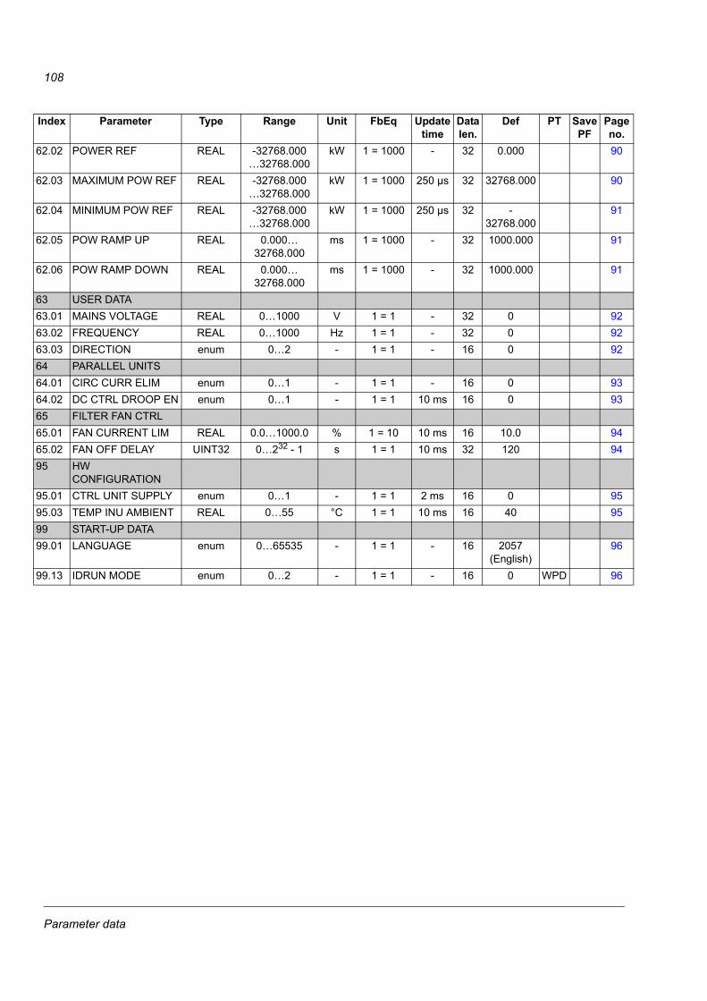
Parameter data
108
62.02 POWER REF REAL -32768.000…32768.000
kW 1 = 1000 - 32 0.000 90
62.03 MAXIMUM POW REF REAL -32768.000…32768.000
kW 1 = 1000 250 µs 32 32768.000 90
62.04 MINIMUM POW REF REAL -32768.000…32768.000
kW 1 = 1000 250 µs 32 -32768.000
91
62.05 POW RAMP UP REAL 0.000…32768.000
ms 1 = 1000 - 32 1000.000 91
62.06 POW RAMP DOWN REAL 0.000…32768.000
ms 1 = 1000 - 32 1000.000 91
63 USER DATA63.01 MAINS VOLTAGE REAL 0…1000 V 1 = 1 - 32 0 9263.02 FREQUENCY REAL 0…1000 Hz 1 = 1 - 32 0 9263.03 DIRECTION enum 0…2 - 1 = 1 - 16 0 9264 PARALLEL UNITS64.01 CIRC CURR ELIM enum 0…1 - 1 = 1 - 16 0 9364.02 DC CTRL DROOP EN enum 0…1 - 1 = 1 10 ms 16 0 9365 FILTER FAN CTRL65.01 FAN CURRENT LIM REAL 0.0…1000.0 % 1 = 10 10 ms 16 10.0 9465.02 FAN OFF DELAY UINT32 0…232 - 1 s 1 = 1 10 ms 32 120 9495 HW
CONFIGURATION95.01 CTRL UNIT SUPPLY enum 0…1 - 1 = 1 2 ms 16 0 9595.03 TEMP INU AMBIENT REAL 0…55 °C 1 = 1 10 ms 16 40 9599 START-UP DATA99.01 LANGUAGE enum 0…65535 - 1 = 1 - 16 2057
(English)96
99.13 IDRUN MODE enum 0…2 - 1 = 1 - 16 0 WPD 96
Index Parameter Type Range Unit FbEq Update time
Data len.
Def PT Save PF
Page no.

Fault tracing
109
Fault tracing
What this chapter containsThe chapter lists all alarm and fault messages including the possible cause and corrective actions.
Safety
WARNING! Only qualified electricians are allowed to maintain the drive. The Safety Instructions on the first pages of the appropriate hardware manual must be read before you start working with the drive.
Alarm and fault indicationsAn alarm or a fault message indicates abnormal drive status. Most alarm and fault causes can be identified and corrected using this information. If not, an ABB representative should be contacted.
The four-digit code number in brackets after the message is for the fieldbus communication.
The alarm/fault code is displayed on the 7-segment display of the drive. The following table describes the indications given by the 7-segment display.
How to resetThe drive can be reset either by pressing the reset key on the PC tool ( ) or control panel (RESET) or switching the supply voltage off for a while. When the fault has been removed, the motor can be restarted.
A fault can also be reset from an external source by parameter 10.08 FAULT RESET SEL.
Display Meaning
“E-” followed by error code
System error. See appropriate drive hardware manual.
“A-” followed by error code
Alarm. See section Alarm messages generated by the drive on page 111.
“F-” followed by error code
Fault. See section Fault messages generated by the drive on page 115.

Fault tracing
110
Fault historyWhen fault is detected, it is stored in the fault logger with a time stamp. The fault history stores information on the 16 latest faults of the drive. Three of the latest faults are stored at the beginning of a power switch off.
Signals 8.01 ACTIVE FAULT and 8.02 LAST FAULT store the fault codes of the most recent faults.
Alarms can be monitored via alarm words 8.05 ALARM WORD 1 … 8.08 ALARM WORD 4. Alarm information is lost at power switch off or fault reset.

Fault tracing
111
Alarm messages generated by the driveCode Alarm
(fieldbus code)Cause What to do
2003 SAFE TORQUE OFF(0xFF7A)Programmable fault: 46.07 STO DIAGNOSTIC
Safe Torque Off function is active, i.e. safety circuit signal(s) connected to connector X6 is lost while drive is stopped and parameter 46.07 STO DIAGNOSTIC is set to (2) ALARM.
Check safety circuit connections. For more information, see appropriate drive hardware manual.
2004 STO MODE CHANGE(0xFF7A)
Error in changing Safe Torque Off supervision, i.e. parameter 46.07 STO DIAGNOSTIC setting could not be changed to value (2) ALARM.
Contact your local ABB representative.
2005 EXT TEMPERATURE(0x4310)Programmable fault: 45.01 EXT TEMP PROT
Measured temperature or resistance (selected by parameter 45.02 EXT TEMP SOURCE) has exceeded alarm limit defined by parameter 45.03 EXT TEMP ALM LIM.
Check that thermistor signal is connected to the input selected by parameter 45.02 EXT TEMP SOURCE.Check that thermistor type is the one selected by parameter 45.02 EXT TEMP SOURCE.Check the value of the alarm limit (45.03).
2006 EMERGENCY OFF(0xF083)
Drive has received emergency OFF2 command.
To restart drive, activate RUN ENABLE signal (source selected by parameter 10.09 RUN ENABLE) and start drive.
2007 RUN ENABLE(0xFF54)
No Run enable signal is received.
Check setting of parameter 10.09 RUN ENABLE. Switch signal on (e.g. in the fieldbus Control Word) or check wiring of selected source.
2008 ID-RUN(0xFF84)
Network identification is requested by parameter 99.13 IDRUN MODE = Normal.
Start the identification routine by pressing the Start button. The identification routine initializes parameters 63.01…63.03 and it lasts for a few seconds. Modulation stops and the warning disappears after the identification is completed.Select 99.13 IDRUN MODE = Clear Results to cancel a pending identification request.
2009 EMERGENCY STOP(0xF081)
Drive has received emergency stop command (OFF1/OFF3).
Check that it is safe to continue operation.Return emergency stop push button to normal position (or adjust the fieldbus Control Word accordingly).Restart drive.
2011 BR OVERHEAT(0x7112)
Brake resistor temperature has exceeded alarm limit defined by parameter 48.07 BR TEMP ALARMLIM.
Stop drive. Let resistor cool down. Check resistor overload protection function settings, parameters 48.01…48.05.Check alarm limit setting, parameter 48.07.Check that braking cycle meets allowed limits.

Fault tracing
112
2012 BC OVERHEAT(0x7181)
Brake chopper IGBT temperature has exceeded internal alarm limit.
Let chopper cool down. Check resistor overload protection function settings, parameters 48.01…48.05.Check that braking cycle meets allowed limits.Check that drive supply AC voltage is not excessive.
2013 DEVICE OVERTEMP(0x4210)
Measured drive temperature has exceeded internal alarm limit.
Check ambient conditions.Check air flow and fan operation.Check heatsink fins for dust pick-up.Check motor power against unit power.
2014 INTBOARD OVERTEMP(0x7182)
Interface board (between power unit and control unit) temperature has exceeded internal alarm limit.
Let drive cool down.
2015 BC MOD OVERTEMP(0x7183)
Input bridge or brake chopper temperature has exceeded internal alarm limit.
Let drive cool down.
2016 IGBT OVERTEMP(0x7184)
Drive temperature based on thermal model has exceeded internal alarm limit.
Check ambient conditions.Check air flow and fan operation.Check heatsink fins for dust pick-up.Check motor power against unit power.
2017 FIELDBUS COMM(0x7510)Programmable fault: 50.02 COMM LOSS FUNC
Cyclical communication between drive and fieldbus adapter module or between PLC and fieldbus adapter module is lost.
Check status of fieldbus communication. See appropriate User’s Manual of fieldbus adapter module.Check fieldbus parameter settings. See parameter group 50 FIELDBUS on page 75.Check cable connections.Check if communication master can communicate.
2018 LOCAL CTRL LOSS(0x5300)Programmable fault: 46.03 LOCAL CTRL LOSS
Control panel or PC tool selected as active control location for drive has ceased communicating.
Check PC tool or control panel connection.Check control panel connector.Replace control panel in mounting platform.
2019 AI SUPERVISION(0x8110)Programmable fault: 13.12 AI SUPERVISION
Analogue input AI1 or AI2 signal has reached limit defined by parameter 13.13 AI SUPERVIS ACT.
Check analogue input AI1/2 source and connections. Check analogue input AI1/2 minimum and maximum limit settings, parameters 13.02 and 13.03 / 13.07 and 13.08.
2020 FB PAR CONF(0x6320)
The drive does not have a functionality requested by PLC, or requested functionality has not been activated.
Check PLC programming.Check fieldbus parameter settings. See parameter group 50 FIELDBUS on page 75.
Code Alarm(fieldbus code)
Cause What to do

Fault tracing
113
2033 D2D COMMUNICATION(0x7520)Programmable fault: 57.02 COMM LOSS FUNC
On the master drive: The drive has not received a response from an activated follower for five consecutive polling cycles.
Check that all drives that are polled (parameters 57.04 and 57.05) on the drive-to-drive link are powered, properly connected to the link, and have the correct node address.Check the drive-to-drive link wiring.
On a follower drive: The drive has not received new reference 1 and/or 2 for five consecutive reference handling cycles.
Check parameter settings to ensure that all followers in the multicast message chain (i.e. when parameter 57.11 REF 1 MSG TYPE = REF1 MC GRPS on the master) receive a reference 1 and command word.Check that the handling of reference 2 is not disabled (i.e. disabled by setting input pin 'Ref2 Cycle Sel' of the D2D_Conf block to negative) in the application program of the master drive.Check the drive-to-drive link wiring.
2034 D2D BUFFER OVERLOAD(0x7580)Programmable fault: 57.02 COMM LOSS FUNC
Transmission of drive-to-drive references failed because of message buffer overflow.
If an application program exists: Check the selected reference handling cycles from the D2D_Conf block in the application program to verify that a maximum of eight messages per millisecond is not exceeded. Check the number of D2D_SendMessage blocks, sum of active D2D_SendMessage blocks and that reference 2 message (if not disabled) is not above four.Check the drive-to-drive link wiring.
2035 PS COMM(0x5480)
Communication errors detected between the JCU Control Unit and the power unit of the drive.
Check the connections between the JCU Control Unit and the power unit.
2036 RESTORE(0x630D)
Restoration of backed-up parameters failed.
Contact your local ABB representative.
2039 EARTH FAULT(0x2330)Programmable fault: 46.05 EARTH FAULT
The regen supply module has detected that there is a too large current imbalance between measured phase currents.
If the supply modules are parallel-connected, disable earth fault supervision in the supply modules.Check that there is no earth fault in supply cables. If no earth fault can be detected, contact your local ABB representative.
2042 D2D CONFIG(0x7583)
The settings of drive-to-drive link configuration parameters (group 57) are incompatible.
Check the settings of the parameters in group 57 D2D COMMUNICATION.Parameter mismatch in master drive: 57.11 REF 1 MSG TYPE = REF1 MC GRPS but the 57.13 NEXT REF1 MC GRP = 0. Give the correct target node.
2050 IGBT OVERLOAD(0x5482)
Excessive IGBT junction to case temperature. This fault protects the IGBT(s) and can be activated by a short circuit in the motor cable.
Check motor cable.
Code Alarm(fieldbus code)
Cause What to do

Fault tracing
114
2051 IGBT TEMP(0x4210)
Drive IGBT temperature is excessive. Fault trip limit is 100%.
Check ambient conditions.Check air flow and fan operation.Check heatsink fins for dust pick-up.Check motor power against drive power.
2052 COOLING(0x4290)
Drive module temperature is excessive.
Check ambient temperature. If it exceeds 40 °C (104 °F), ensure that load current does not exceed derated load capacity of drive. See appropriate Hardware Manual.Check drive module cooling air flow and fan operation.Check inside of cabinet and heatsink of drive module for dust pick-up. Clean whenever necessary.
2072 DC NOT CHARGED(0x3250)
Starting has been attempted before charging of the intermediate circuit is finished.
Wait a moment for the DC voltage to rise. Check from parameter 1.07 DC-VOLTAGE that the supply voltage is high enough.Change 47.03 SUPPLVOLTAUTO-ID = Disable and set appropriate value to 47.04 SUPPLY VOLTAGE.If 47.03 SUPPLVOLTAUTO-ID = Disable, check that the value of 47.04 corresponds to the mains voltage of the supply network.
Code Alarm(fieldbus code)
Cause What to do

Fault tracing
115
Fault messages generated by the driveCode Fault
(fieldbus code)Cause What to do
0001 OVERCURRENT(0x2310)
Output current has exceeded internal fault limit.
Check motor load.Check supply voltage.Check that there are no power factor compensation capacitors in the supply.Check converter power semiconductors (IGBTs) and current transducers.
0002 DC OVERVOLTAGE(0x3210)
Excessive intermediate circuit DC voltage.
Check that overvoltage controller is on in the motor drives (if applicable).Check deceleration time of the motor drives.Check brake chopper and resistor (if used).Check mains for static or transient overvoltage.
0003 DEVICE OVERTEMP(0x4210)
Measured drive temperature has exceeded internal fault limit.
Check ambient conditions.Check air flow and fan operation.Check heatsink fins for dust pick-up.Check motor power against unit power.
0004 SHORT CIRCUIT(0x2340)
Fast overcurrent indicating short circuit fault.
See the OVERCURRENT fault.Measure resistances of converter power semiconductors (IGBTs). If faulty IGBTs are found, contact your local ABB representative.
0005 DC UNDERVOLTAGE(0x3220)
Intermediate circuit DC voltage is not sufficient due to missing mains phase, blown fuse or converter internal fault.
Check mains supply and fuses.
0006 EARTH FAULT(0x2330)Programmable fault: 46.05 EARTH FAULT
The regen supply module has detected that there is a too large current imbalance between measured phase currents.
If the supply modules are parallel-connected, earth fault supervision must be disabled.Check converter fuses.Check that there is no earth fault in supply cables. If no earth fault can be detected, contact your local ABB representative.
0007 FAN FAULT(0xFF83)
Fan is not able to rotate freely or fan is disconnected. Fan operation is monitored by measuring fan current.
Check fan operation and connection.
0008 IGBT OVERTEMP(0x7184)
Drive temperature based on thermal model has exceeded internal fault limit.
Check ambient conditions.Check air flow and fan operation.Check heatsink fins for dust pick-up.Check motor power against unit power.
0009 BC WIRING(0x7111)
Brake resistor short circuit or brake chopper control fault.
Check brake chopper and brake resistor connection.Ensure brake resistor is not damaged.

Fault tracing
116
0010 BC SHORT CIRCUIT(0x7113)
Short circuit in brake chopper IGBT.
Ensure brake resistor is connected and not damaged.
0011 BC OVERHEAT(0x7181)
Brake chopper IGBT temperature has exceeded internal fault limit.
Let chopper cool down. Check resistor overload protection function settings, parameters 48.03…48.05.Check that braking cycle meets allowed limits.Check that drive supply AC voltage is not excessive.
0012 BR OVERHEAT(0x7112)
Brake resistor temperature has exceeded fault limit defined by parameter 48.06 BR TEMP FAULTLIM.
Stop drive. Let resistor cool down. Check resistor overload protection function settings, parameters 48.01…48.05.Check fault limit setting, parameter 48.06.Check that braking cycle meets allowed limits.
0015 SUPPLY PHASE(0x3130)Programmable fault: 46.06 SUPPL PHS LOSS
Missing phase during synchronization.
Check supply fuses.Check supply for network imbalance.
0018 CURR U2 MEAS(0x3184)
Measured offset error of U2 output phase current measurement is too great. (Offset value is updated during current calibration.)
Contact your local ABB representative.
0019 CURR V2 MEAS(0x3185)
Measured offset error of V2 output phase current measurement is too great. (Offset value is updated during current calibration.)
Contact your local ABB representative.
0020 CURR W2 MEAS(0x3186)
Measured offset error of W2 output phase current measurement is too great. (Offset value is updated during current calibration.)
Contact your local ABB representative.
0021 STO1 LOST(0x8182)
Safe Torque Off function is active, i.e. safety circuit signal 1 connected between X6:1 and X6:3 is lost while drive is at stopped state and parameter 46.07 STO DIAGNOSTIC setting is (2) ALARM or (3) NO.
Check safety circuit connections. For more information, see appropriate drive hardware manual.
Code Fault(fieldbus code)
Cause What to do

Fault tracing
117
0022 STO2 LOST(0x8183)
Safe Torque Off function is active, i.e. safety circuit signal 2 connected between X6:2 and X6:4 is lost while drive is at stopped state and parameter 46.07 STO DIAGNOSTIC setting is (2) ALARM or (3) NO.
Check safety circuit connections. For more information, see appropriate drive hardware manual.
0023 STO MODE CHANGE(0xFF7A)
Error in changing Safe Torque Off supervision, i.e. parameter 46.07 STO DIAGNOSTIC setting could not be changed to value (1) FAULT.
Contact your local ABB representative.
0024 INTBOARD OVERTEMP(0x7182)
Interface board (between power unit and control unit) temperature has exceeded internal fault limit.
Let drive cool down.
0025 BC MOD OVERTEMP(0x7183)
Input bridge or brake chopper temperature has exceeded internal fault limit.
Let drive cool down.
0027 PU LOST(0x5400)
Connection between the JCU Control Unit and the power unit of the drive is lost.External 24 V supply connected to JCU without mains supply, but not configured with parameter.
Check the connections between the JCU Control Unit and the power unit.Check the setting of parameter 95.01 CTRL UNIT SUPPLY.
0028 PS COMM(0x5480)
Communication errors detected between the JCU Control Unit and the power unit of the drive.
Check the connections between the JCU Control Unit and the power unit.
0030 EXTERNAL(0x9000)
Fault in external device. (This information is configured through one of programmable digital inputs.)
Check external devices for faults.Check setting of parameter 46.01 EXTERNAL FAULT.
0031 SAFE TORQUE OFF(0xFF7A)Programmable fault: 46.07 STO DIAGNOSTIC
Safe Torque Off function is active, i.e. safety circuit signal(s) connected to connector X6 is lost - during drive start or drive run or- while drive is stopped and parameter 46.07 STO DIAGNOSTIC setting is (1) FAULT.
Check safety circuit connections. For more information, see appropriate drive hardware manual.
0036 LOCAL CTRL LOSS(0x5300)Programmable fault: 46.03 LOCAL CTRL LOSS
Control panel or PC tool selected as active control location for drive has ceased communicating.
Check PC tool or control panel connection.Check control panel connector.Replace control panel in mounting platform.
Code Fault(fieldbus code)
Cause What to do

Fault tracing
118
0037 NVMEM CORRUPTED(0x6320)
Drive internal faultNote: This fault cannot be reset.
Contact your local ABB representative.
0038 OPTION COMM LOSS(0x7000)
Communication to FIO-xx option(s) is lost.
Check that option modules are properly connected to Slot 1 and (or) Slot 2.Check that option modules or Slot 1/2 connectors are not damaged. To determine whether module or connector is damaged: Test each module individually in Slot 1 and Slot 2.
0045 FIELDBUS COMM(0x7510)Programmable fault: 50.02 COMM LOSS FUNC
Cyclical communication between drive and fieldbus adapter module or between PLC and fieldbus adapter module is lost.
Check status of fieldbus communication. See appropriate User’s Manual of fieldbus adapter module.Check fieldbus parameter settings. See parameter group 50 FIELDBUS on page 75.Check cable connections.Check if communication master can communicate.
0046 FB MAPPING FILE(0x6306)
Drive internal fault Contact your local ABB representative.
0047 EXT OVERTEMP(0x4310)Programmable fault: 45.01 EXT TEMP PROT
Measured temperature or resistance (selected by parameter 45.02) has exceeded the fault limit defined by parameter 45.04 EXT TEMP FLT LIM.
Check that thermistor signal is connected to the input selected by parameter 45.02 EXT TEMP SOURCE. Check that thermistor type is the one selected by parameter 45.02 EXT TEMP SOURCE.Check value of fault limit (45.04).
0049 AI SUPERVISION(0x8110)Programmable fault: 13.12 AI SUPERVISION
Analogue input AI1 or AI2 signal has reached limit defined by parameter 13.13 AI SUPERVIS ACT.
Check analogue input AI1/2 source and connections. Check analogue input AI1/2 minimum and maximum limit settings, parameters 13.02 and 13.03 / 13.07 and 13.08.
0052 D2D CONFIG(0x7583)
Configuration of the drive-to-drive link has failed for a reason other than those indicated by alarm 2042, for example start inhibition is requested but not granted.
Contact your local ABB representative.
Code Fault(fieldbus code)
Cause What to do

Fault tracing
119
0053 D2D COMMUNICATION(0x7520)Programmable fault: 57.02 COMM LOSS FUNC
On the master drive: The drive has not received a response from an activated follower for five consecutive polling cycles.
Check that all drives that are polled (parameters 57.04 FOLLOWER MASK 1 and 57.05 FOLLOWER MASK 2) on the drive-to-drive link are powered, properly connected to the link, and have the correct node address.Check the drive-to-drive link wiring.
On a follower drive: The drive has not received new reference 1 and/or 2 for five consecutive reference handling cycles.
Check parameter settings to ensure that all followers in the multicast message chain (i.e. when parameter 57.11 REF 1 MSG TYPE = REF1 MC GRPS on the master) receive a reference 1 and command word.Check that the handling of reference 2 is not disabled (i.e. disabled by setting input pin 'Ref2 Cycle Sel' of the D2D_Conf block to negative) in the application program of the master drive.Check the drive-to-drive link wiring.
0054 D2D BUFFER OVERLOAD(0x7580)Programmable fault: 57.02 COMM LOSS FUNC
Transmission of drive-to-drive references failed because of message buffer overflow.
If an application program exists: Check the selected reference handling cycles in D2D_Conf block in application program to verify that a maximum of eight messages in millisecond is not exceeded. Check the number of D2D_SendMessage blocks; sum of active D2D_SendMessage blocks and that reference 2 message (if not disabled) is not above four.Check the drive-to-drive link wiring.
0055 TECH LIB(0x6382)
Resettable fault generated by a technology library.
Refer to the documentation of the technology library.
0056 TECH LIB CRITICAL(0x6382)
Permanent fault generated by a technology library.
Refer to the documentation of the technology library.
0057 FORCED TRIP(0xFF90)
Generic Drive Communication Profile trip command.
Check PLC status.
0058 FIELDBUS PAR ERROR(0x6320)
The drive does not have a functionality requested by PLC, or requested functionality has not been activated.
Check PLC programming.Check fieldbus parameter settings. See parameter group 50 FIELDBUS on page 75.
0062 D2D SLOT COMM(0x7584)
Drive-to-drive link is set to use an FMBA module for communication, but no module is detected in specified slot.
Check the settings of parameters 57.01 LINK MODE and 57.15 D2D COMM PORT. Ensure that the FMBA module has been detected by checking parameters 9.20…9.22.Try installing the FMBA module into another slot. If the problem persists, contact your local ABB representative.
Code Fault(fieldbus code)
Cause What to do
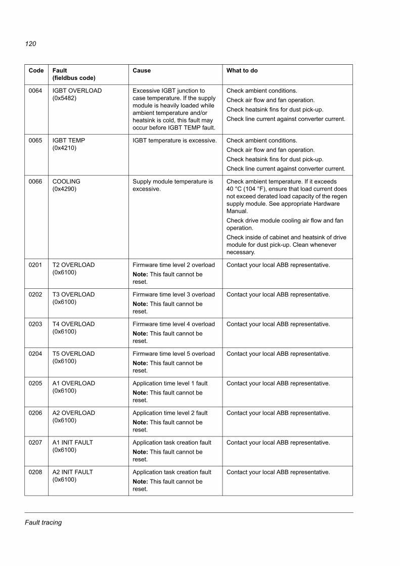
Fault tracing
120
0064 IGBT OVERLOAD(0x5482)
Excessive IGBT junction to case temperature. If the supply module is heavily loaded while ambient temperature and/or heatsink is cold, this fault may occur before IGBT TEMP fault.
Check ambient conditions.Check air flow and fan operation.Check heatsink fins for dust pick-up.Check line current against converter current.
0065 IGBT TEMP(0x4210)
IGBT temperature is excessive. Check ambient conditions.Check air flow and fan operation.Check heatsink fins for dust pick-up.Check line current against converter current.
0066 COOLING(0x4290)
Supply module temperature is excessive.
Check ambient temperature. If it exceeds 40 °C (104 °F), ensure that load current does not exceed derated load capacity of the regen supply module. See appropriate Hardware Manual.Check drive module cooling air flow and fan operation.Check inside of cabinet and heatsink of drive module for dust pick-up. Clean whenever necessary.
0201 T2 OVERLOAD(0x6100)
Firmware time level 2 overloadNote: This fault cannot be reset.
Contact your local ABB representative.
0202 T3 OVERLOAD(0x6100)
Firmware time level 3 overloadNote: This fault cannot be reset.
Contact your local ABB representative.
0203 T4 OVERLOAD(0x6100)
Firmware time level 4 overloadNote: This fault cannot be reset.
Contact your local ABB representative.
0204 T5 OVERLOAD(0x6100)
Firmware time level 5 overloadNote: This fault cannot be reset.
Contact your local ABB representative.
0205 A1 OVERLOAD(0x6100)
Application time level 1 faultNote: This fault cannot be reset.
Contact your local ABB representative.
0206 A2 OVERLOAD(0x6100)
Application time level 2 faultNote: This fault cannot be reset.
Contact your local ABB representative.
0207 A1 INIT FAULT(0x6100)
Application task creation faultNote: This fault cannot be reset.
Contact your local ABB representative.
0208 A2 INIT FAULT(0x6100)
Application task creation faultNote: This fault cannot be reset.
Contact your local ABB representative.
Code Fault(fieldbus code)
Cause What to do

Fault tracing
121
0209 STACK ERROR(0x6100)
Drive internal faultNote: This fault cannot be reset.
Contact your local ABB representative.
0210 JMU MISSING(0xFF61)
JMU Memory Unit is missing or broken.
Ensure that JMU is in its place and properly connected.Replace broken JMU.
0301 UFF FILE READ(0x6300)
File read errorNote: This fault cannot be reset.
Contact your local ABB representative.
0302 APPL DIR CREATION(0x6100)
Drive internal faultNote: This fault cannot be reset.
Contact your local ABB representative.
0303 FPGA CONFIG DIR(0x6100)
Drive internal faultNote: This fault cannot be reset.
Contact your local ABB representative.
0304 PU RATING ID(0x5483)
Drive internal faultNote: This fault cannot be reset.
Contact your local ABB representative.
0305 RATING DATABASE(0x6100)
Drive internal faultNote: This fault cannot be reset.
Contact your local ABB representative.
0306 LICENSING(0x6100)
Drive internal faultNote: This fault cannot be reset.
Contact your local ABB representative.
0307 DEFAULT FILE(0x6100)
Drive internal faultNote: This fault cannot be reset.
Contact your local ABB representative.
0308 APPL FILE PAR CONF (0x6300)
Corrupted application fileNote: This fault cannot be reset.
Reload application.If fault is still active, contact your local ABB representative.
0309 APPL LOADING(0x6300)
Corrupted application fileNote: This fault cannot be reset.
Reload application.If fault is still active, contact your local ABB representative.
0310 USERSET LOAD(0xFF69)
Loading of user set is not successfully completed because:- requested user set does not exist- user set is not compatible with drive program- drive has been switched off during loading.
Reload.
Code Fault(fieldbus code)
Cause What to do
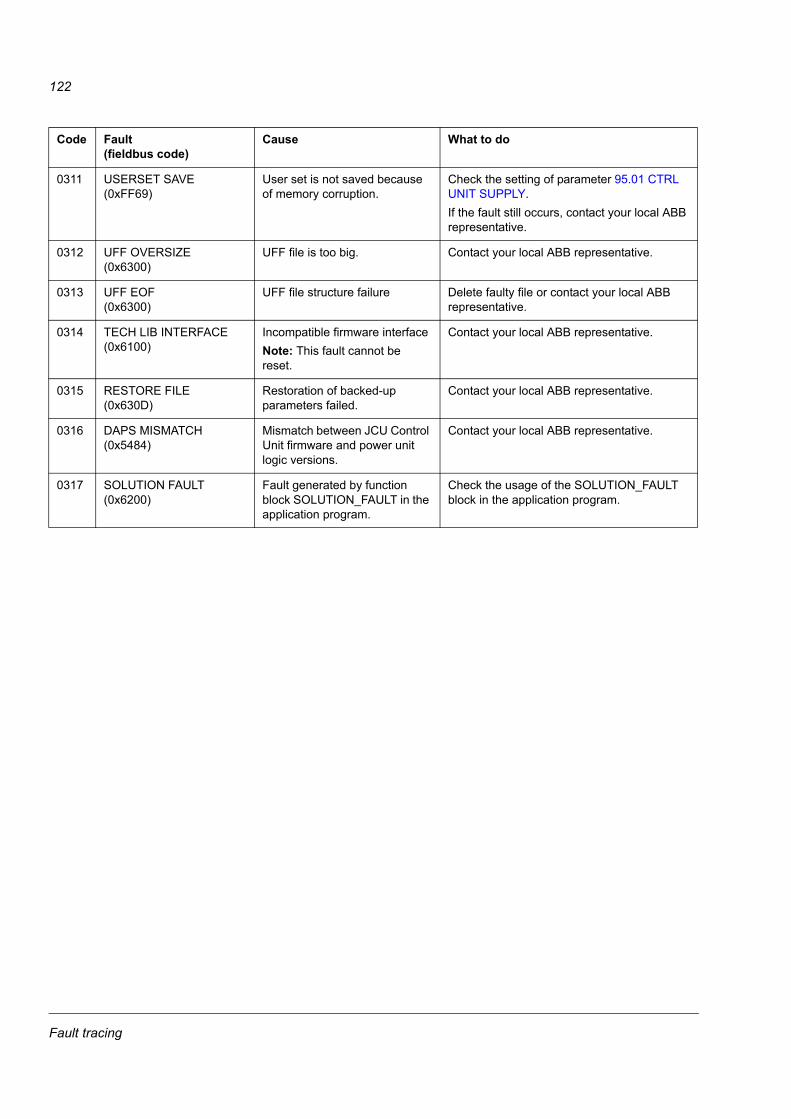
Fault tracing
122
0311 USERSET SAVE(0xFF69)
User set is not saved because of memory corruption.
Check the setting of parameter 95.01 CTRL UNIT SUPPLY.If the fault still occurs, contact your local ABB representative.
0312 UFF OVERSIZE(0x6300)
UFF file is too big. Contact your local ABB representative.
0313 UFF EOF(0x6300)
UFF file structure failure Delete faulty file or contact your local ABB representative.
0314 TECH LIB INTERFACE(0x6100)
Incompatible firmware interfaceNote: This fault cannot be reset.
Contact your local ABB representative.
0315 RESTORE FILE(0x630D)
Restoration of backed-up parameters failed.
Contact your local ABB representative.
0316 DAPS MISMATCH(0x5484)
Mismatch between JCU Control Unit firmware and power unit logic versions.
Contact your local ABB representative.
0317 SOLUTION FAULT(0x6200)
Fault generated by function block SOLUTION_FAULT in the application program.
Check the usage of the SOLUTION_FAULT block in the application program.
Code Fault(fieldbus code)
Cause What to do

Application program template
123
Application program template
What this chapter containsThis chapter presents the application program template as displayed by the DriveSPC tool.

Application program template
124
AC
TU
AL V
AL
UE
S8
TLF11 2 m
sec
(1)
1.0
3 F
REQ
UENCY
1.0
4 C
URR
EN
T
1.0
5 C
URR
EN
T P
ER
C
1.0
7 D
C-V
OLT
AG
E
1.1
5 T
EM
P I
NVER
TER
1.1
6 T
EM
P B
C
1.2
0 B
RAKE R
ES L
OAD
1.2
2 I
NV
ERTER P
OW
ER
1.2
6 O
N T
IME C
OU
NTER
1.2
7 R
UN T
IME C
OU
NTER
1.2
8 F
AN
ON
-TIM
E
Page 1
Sig
nals
FW
A c
om
patibility level =
0.6
0
Firm
ware
Lib
rary
ID
= 1
, ver
= 1
.0
Sta
ndard
Lib
rary
ID =
10000, ver
= 1
.1
Based o
n
Cust
om
er
Cust
. D
oc. N
o.
Date
Pre
pare
d
Appro
ved
Pro
ject
nam
e
Title
Doc. des.
Resp. dept.
Doc. N
o.
Application program template
125
DI
10
TLF8
2 m
sec
(1)
12.1
3 D
I IN
VE
RT M
ASK
(Drive v
alu
e)
2.0
1 D
I STA
TU
S
RO
11
TLF8
2 m
sec
(2)
< 1
2.1
2 R
O1 O
UT P
TR
(Drive v
alu
e)
2.0
2 R
O S
TATU
S
DIO
112
TLF8
2 m
sec
(3)
1
2.0
1 D
IO1 C
ON
F(D
rive v
alu
e)
< 1
2.0
4 D
IO1 O
UT P
TR
(Drive v
alu
e)
2.0
3 D
IO S
TAT
US
2.0
3
Bit 0
DIO
213
TLF8
2 m
sec
(4)
1
2.0
2 D
IO2 C
ON
F(D
rive v
alu
e)
< 1
2.0
5 D
IO2 O
UT P
TR
(Drive v
alu
e)
1
2.1
4 D
IO2 F
MAX
(Drive v
alu
e)
1
2.1
5 D
IO2 F
MIN
(Drive v
alu
e)
1
2.1
6 D
IO2 F
MAX S
CALE
(Drive v
alu
e)
1
2.1
7 D
IO2 F
MIN
SCALE
(Drive v
alu
e)
2.0
3 D
IO S
TAT
US
2.0
3
Bit 1
2.1
0 D
IO2 F
REQ
IN
DIO
314
TLF8
2 m
sec
(5)
1
2.0
3 D
IO3 C
ON
F(D
rive v
alu
e)
< 1
2.0
6 D
IO3 O
UT P
TR
(Drive v
alu
e)
< 1
2.0
7 D
IO3 F
OU
T P
TR
[ D
C-V
OLTAG
E ]
(1 /
1.0
7)
1
2.0
8 D
IO3 F
MAX
(Drive v
alu
e)
1
2.0
9 D
IO3 F
MIN
(Drive v
alu
e)
1
2.1
0 D
IO3 F
MAX S
CALE
(Drive v
alu
e)
1
2.1
1 D
IO3 F
MIN
SCALE
(Drive v
alu
e)
2.0
3 D
IO S
TAT
US
2.0
3
Bit 2
2.1
1 D
IO3 F
REQ
OUT
Page 2
Dig
ital I/
O
FW
A c
om
patibility level =
0.6
0
Firm
ware
Lib
rary
ID
= 1
, ver
= 1
.0
Sta
ndard
Lib
rary
ID =
10000, ver
= 1
.1
Based o
n
Cust
om
er
Cust
. D
oc. N
o.
Date
Pre
pare
d
Appro
ved
Pro
ject
nam
e
Title
Doc. des.
Resp. dept.
Doc. N
o.
Application program template
126
AI1
17
TLF8
2 m
sec
(6)
13.0
1 A
I1 F
ILT T
IME
(Drive v
alu
e)
13.0
2 A
I1 M
AX
(Drive v
alu
e)
13.0
3 A
I1 M
IN(D
rive v
alu
e)
13.0
4 A
I1 M
AX S
CALE
(Drive v
alu
e)
13.0
5 A
I1 M
IN S
CALE
(Drive v
alu
e)
2.0
4 A
I1
2.0
5 A
I1 S
CALED
AI2
18
TLF8
2 m
sec
(7)
13.0
6 A
I2 F
ILT T
IME
(Drive v
alu
e)
13.0
7 A
I2 M
AX
(Drive v
alu
e)
13.0
8 A
I2 M
IN(D
rive v
alu
e)
13.0
9 A
I2 M
AX S
CALE
(Drive v
alu
e)
13.1
0 A
I2 M
IN S
CALE
(Drive v
alu
e)
2.0
6 A
I2
2.0
7 A
I2 S
CALED
AO
119
TLF8
2 m
sec
(8)
< 1
5.0
1 A
O1 P
TR
[ CU
RRENT P
ERC ]
(1 /
1.0
5)
1
5.0
2 A
O1 F
ILT T
IME
(Drive v
alu
e)
1
5.0
3 A
O1 M
AX
(Drive v
alu
e)
1
5.0
4 A
O1 M
IN(D
rive v
alu
e)
1
5.0
5 A
O1 M
AX S
CALE
(Drive v
alu
e)
1
5.0
6 A
O1 M
IN S
CALE
(Drive v
alu
e)
2.0
8 A
O1
AO
220
TLF8
2 m
sec
(9)
< 1
5.0
7 A
O2 P
TR
[ D
C-V
OLTAG
E ]
(1 /
1.0
7)
1
5.0
8 A
O2 F
ILT T
IME
(Drive v
alu
e)
1
5.0
9 A
O2 M
AX
(Drive v
alu
e)
1
5.1
0 A
O2 M
IN(D
rive v
alu
e)
1
5.1
1 A
O2 M
AX S
CALE
(Drive v
alu
e)
1
5.1
2 A
O2 M
IN S
CALE
(Drive v
alu
e)
2.0
9 A
O2
Page 3
Analo
g I
/O
FW
A c
om
patibility level =
0.6
0
Firm
ware
Lib
rary
ID
= 1
, ver
= 1
.0
Sta
ndard
Lib
rary
ID =
10000, ver
= 1
.1
Based o
n
Cust
om
er
Cust
. D
oc. N
o.
Date
Pre
pare
d
Appro
ved
Pro
ject
nam
e
Title
Doc. des.
Resp. dept.
Doc. N
o.
Application program template
127
RE
FE
REN
CE
CTR
L23
TLF
9 250
µse
c(4
)
< 3
4.0
1 E
XT1/E
XT2 S
EL
(Drive
val
ue)
3
4.0
3 E
XT1 C
TR
L M
OD
E1
(Drive
val
ue)
3
4.0
5 E
XT2 C
TR
L M
OD
E1
(Drive
val
ue)
3
4.0
7 L
OCAL
CTR
L M
OD
E(D
rive
val
ue)
6.1
2 O
P M
OD
E A
CK
FIE
LD
BU
S30
TLF
10
500
µse
c(1
)
5
0.0
1 F
BA E
NABLE
(Drive
val
ue)
5
0.0
2 C
OM
M L
OSS F
UN
C(D
rive
val
ue)
5
0.0
3 C
OM
M L
OSS T
OU
T(D
rive
val
ue)
5
0.0
4 F
BA R
EF1 S
CALE
(Drive
val
ue)
5
0.0
5 F
BA R
EF2 S
CALE
(Drive
val
ue)
< 5
0.0
6 F
BA A
CT1 S
EL
[ D
C-V
OLT
AG
E ]
(1 /
1.0
7)
< 5
0.0
7 F
BA A
CT2 S
EL
[ R
EACTIV
E PO
WER
]
(6 /
4.0
1)
< 5
0.0
8 F
BA S
W B
12 S
RC
(Drive
val
ue)
< 5
0.0
9 F
BA S
W B
13 S
RC
(Drive
val
ue)
< 5
0.1
0 F
BA S
W B
14 S
RC
(Drive
val
ue)
< 5
0.1
1 F
BA S
W B
15 S
RC
(Drive
val
ue)
2.1
2 F
BA M
AIN
CW
2.1
3 F
BA M
AIN
SW
2.1
4 F
BA M
AIN
REF1
2.1
5 F
BA M
AIN
REF2
D2
D C
OM
MU
NIC
AT
IO
N34
TLF
10
500
µse
c(2
)
5
7.0
1 L
INK M
OD
E(D
rive
val
ue)
5
7.0
2 C
OM
M L
OSS F
UN
C(D
rive
val
ue)
5
7.0
3 N
OD
E A
DD
RESS
(Drive
val
ue)
5
7.0
4 F
OLLO
WER M
ASK 1
(Drive
val
ue)
5
7.0
5 F
OLLO
WER M
ASK 2
(Drive
val
ue)
< 5
7.0
6 R
EF 1
SR
C[
DC
-VO
LTA
GE
]
(1 /
1.0
7)
< 5
7.0
7 R
EF 2
SR
C[
DC
-VO
LTA
GE
]
(1 /
1.0
7)
< 5
7.0
8 F
OLLO
WER C
W S
RC
[ D
2D
FO
LLO
WER C
W ]
(4 /
2.1
8)
5
7.0
9 K
ERN
EL S
YN
C M
OD
E(D
rive
val
ue)
5
7.1
0 K
ERN
EL S
YN
C O
FFS
(Drive
val
ue)
5
7.1
1 R
EF 1
MSG
TYPE
(Drive
val
ue)
5
7.1
2 R
EF1 M
C G
RO
UP
(Drive
val
ue)
5
7.1
3 N
EXT R
EF1 M
C G
RP
(Drive
val
ue)
5
7.1
4 N
R R
EF1 M
C G
RPS
(Drive
val
ue)
2.1
7 D
2D
MAIN
CW
2.1
9 D
2D
REF1
2.2
0 D
2D
REF2
DR
IV
E L
OG
IC
15
TLF
11
2 m
sec
(2)
1
0.0
1 E
XT1 S
TA
RT F
UN
C(D
rive
val
ue)
< 1
0.0
2 E
XT1 S
TA
RT I
N1
(Drive
val
ue)
< 1
0.0
3 E
XT1 S
TA
RT I
N2
(Drive
val
ue)
1
0.0
4 E
XT2 S
TA
RT F
UN
C(D
rive
val
ue)
< 1
0.0
5 E
XT2 S
TA
RT I
N1
(Drive
val
ue)
< 1
0.0
6 E
XT2 S
TA
RT I
N2
(Drive
val
ue)
< 1
0.0
8 F
AU
LT R
ESET S
EL
(Drive
val
ue)
< 1
0.0
9 R
UN
EN
ABLE
(Drive
val
ue)
1
0.1
2 S
TA
RT I
NH
IBIT
(Drive
val
ue)
< 1
0.1
3 F
B C
W U
SED
[ FBA M
AIN
CW
]
(4 /
2.1
2)
< 1
0.1
6 D
2D
CW
USED
[ D
2D
MAIN
CW
]
(4 /
2.1
7)
< 1
0.1
7 S
TA
RT E
NABLE
(Drive
val
ue)
< 1
0.1
8 F
ORCE S
TO
P(D
rive
val
ue)
2.1
8 D
2D
FO
LLO
WER C
W
6.0
1 S
TA
TU
S W
ORD
1
6.0
2 S
TA
TU
S W
ORD
2
6.0
5 L
IMIT
WO
RD
1
6.0
7 L
C L
IM S
TATU
S
Pag
e 4 D
rive
Log
ic
FW
A c
ompatibili
ty le
vel =
0.6
0
Firm
ware
Lib
rary
ID
= 1
, ve
r =
1.0
Sta
ndar
d L
ibra
ry I
D =
100
00,
ver
= 1
.1
Base
d o
n
Cust
omer
Cust
. D
oc.
No.
Date
Pre
pare
d
Appro
ved
Pro
ject
nam
e
Title
Doc.
des
.
Res
p.
dep
t.
Doc.
No.

Application program template
128
BR
AK
E C
HO
PP
ER
29
TLF11 2 m
sec
(6)
4
8.0
1 B
C E
NA
BLE
(Drive v
alu
e)
< 4
8.0
2 B
C R
UN
-TIM
E E
NA
(Drive v
alu
e)
4
8.0
3 B
RTH
ERM
TIM
EC
ON
ST
(Drive v
alu
e)
4
8.0
4 B
R P
OW
ER M
AX C
NT
(Drive v
alu
e)
4
8.0
5 R
BR
(Drive v
alu
e)
4
8.0
6 B
R T
EM
P F
AU
LTLI
M(D
rive v
alu
e)
4
8.0
7 B
R T
EM
P A
LARM
LIM
(Drive v
alu
e)
VO
LT
AG
E C
TR
L28
TLF12 10 m
sec
(1)
47.0
3 S
UPPLV
OLTAU
TO
-ID
(Drive v
alu
e)
47.0
4 S
UPPLY
VO
LTAG
E(D
rive v
alu
e)
1.1
9 U
SED
SU
PPLY
VO
LT
US
ER
GR
ID
DA
TA
42
TLF12 10 m
sec
(5)
63.0
1 M
AIN
S V
OLTAG
E(D
rive v
alu
e)
63.0
2 F
REQ
UENC
Y(D
rive v
alu
e)
63.0
3 D
IRECTIO
N(D
rive v
alu
e)
Page 5
Drive C
ontr
ol
FW
A c
om
patibility level =
0.6
0
Firm
ware
Lib
rary
ID
= 1
, ver
= 1
.0
Sta
ndard
Lib
rary
ID =
10000, ver
= 1
.1
Based o
n
Cust
om
er
Cust
. D
oc. N
o.
Date
Pre
pare
d
Appro
ved
Pro
ject
nam
e
Title
Doc. des.
Resp. dept.
Doc. N
o.

Application program template
129
DC
VO
LTA
GE C
TR
L37
TLF9
25
0 µ
sec
(1)
< 6
0.0
1 D
C R
EF S
EL
(Dri
ve v
alu
e)
6
0.0
2 D
C V
OLT R
EF
(Dri
ve v
alu
e)
6
0.0
3 D
C R
EF M
AX
(Dri
ve v
alu
e)
6
0.0
4 D
C R
EF M
IN(D
rive
valu
e)
6
0.0
5 D
C R
AM
P U
P(D
rive
valu
e)
6
0.0
6 D
C R
AM
P D
OW
N(D
rive
valu
e)
4.1
0 D
C R
EF1
4.1
1 D
C R
EF R
AM
P I
N
4.1
2 D
C R
EF R
AM
PED
4.3
4 P
OW
ER
REF U
SED
RE
AC
TIV
E P
OW
ER
CT
RL
38
TLF9
25
0 µ
sec
(2)
< 6
1.0
1 Q
PO
WER
REF S
EL
[ Q
PO
WER R
EF ]
(6 /
61.0
2)
6
1.0
2 Q
PO
WER
REF
(Dri
ve v
alu
e)
6
1.0
3 Q
PO
WER
REF M
AX
(Dri
ve v
alu
e)
6
1.0
4 Q
PO
WER
REF M
IN(D
rive
valu
e)
6
1.0
5 Q
PO
W R
AM
P U
P(D
rive
valu
e)
6
1.0
6 Q
PO
W R
AM
P D
OW
N(D
rive
valu
e)
4.0
1 R
EACTIV
E P
OW
ER
4.2
0 Q
PO
W R
EF
4.2
1 Q
PO
W R
AM
P I
N
4.2
2 Q
PO
W R
EF R
AM
PED
AC
TIV
E P
OW
ER
RE
F39
TLF9
25
0 µ
sec
(3)
< 6
2.0
1 P
OW
REF S
EL
[ PO
WER R
EF ]
(6 /
62.0
2)
6
2.0
2 P
OW
ER
REF
(Dri
ve v
alu
e)
6
2.0
3 M
AX
IMU
M P
OW
REF
(Dri
ve v
alu
e)
6
2.0
4 M
INIM
UM
PO
W R
EF
(Dri
ve v
alu
e)
6
2.0
5 P
OW
RAM
P U
P(D
rive
valu
e)
6
2.0
6 P
OW
RAM
P D
OW
N(D
rive
valu
e)
4.3
0 P
OW
REF1
4.3
1 P
OW
REF R
AM
P I
N
4.3
2 P
OW
REF R
AM
PED
CO
NV
ER
TE
R C
ON
TR
OL
40
TLF1
1 2 m
sec
(4)
40.0
2 S
F R
EF
(Dri
ve v
alu
e)
40.0
4 V
OLT
AG
E R
ESER
VE
(Dri
ve v
alu
e)
64.0
1 C
IRC C
URR
ELIM
(Dri
ve v
alu
e)
64.0
2 D
C C
TR
L D
RO
OP E
N(D
rive
valu
e)
Page
6
Con
ver
ter
Ctr
l
FW
A c
om
patibili
ty lev
el =
0.6
0
Firm
ware
Lib
rary
ID
= 1
, ve
r =
1.0
Sta
ndard
Lib
rary
ID
= 1
0000
, ve
r =
1.1
Base
d o
n
Cust
om
er
Cust
. D
oc.
No.
Date
Pre
par
ed
Appro
ved
Pro
ject
nam
e
Tit
leD
oc.
des.
Res
p.
dept.
Doc.
No.
Application program template
130
LIM
IT
S21
TLF11 2 m
sec
(3)
20.0
5 M
AXIM
UM
CURR
EN
T(D
rive v
alu
e)
FA
ULT
FU
NC
TIO
NS
27
TLF11 2 m
sec
(5)
< 4
6.0
1 E
XTER
NA
L FAU
LT(D
rive v
alu
e)
4
6.0
3 L
OCAL C
TR
L LO
SS
(Drive v
alu
e)
4
6.0
5 E
ARTH
FA
ULT
(Drive v
alu
e)
4
6.0
6 S
UPPL
PH
S L
OSS
(Drive v
alu
e)
4
6.0
7 S
TO
DIA
GN
OSTIC
(Drive v
alu
e)
8.0
1 A
CTIV
E F
AULT
8.0
2 L
AST F
AU
LT
8.0
3 F
AU
LT T
IME H
I
8.0
4 F
AU
LT T
IME L
O
8.0
5 A
LARM
WO
RD
1
8.0
6 A
LARM
WO
RD
2
8.0
7 A
LARM
WO
RD
3
8.0
8 A
LARM
WO
RD
4
EX
T T
HE
RM
PR
OT
26
TLF12 10 m
sec
(2)
45.0
1 E
XT T
EM
P P
RO
T(D
rive v
alu
e)
45.0
2 E
XT T
EM
P S
OU
RCE
(Drive v
alu
e)
45.0
3 E
XT T
EM
P A
LM
LIM
(Drive v
alu
e)
45.0
4 E
XT T
EM
P F
LT L
IM(D
rive v
alu
e)
1.1
7 E
XT T
EM
P
EX
T F
AN
CT
RL
41
TLF12 10 m
sec
(3)
65.0
1 F
AN
CU
RRE
NT L
IM(D
rive v
alu
e)
65.0
2 F
AN
OFF
DELAY
(Drive v
alu
e)
4.0
8 E
XT F
AN
CO
MM
AN
D
SU
PE
RV
IS
IO
N35
TLF12 10 m
sec
(4)
3
3.0
1 S
UPER
V1 F
UN
C(D
rive v
alu
e)
< 3
3.0
2 S
UPER
V1 A
CT
[ D
C-V
OLTAG
E ]
(1 /
1.0
7)
3
3.0
3 S
UPER
V1 L
IM H
I(D
rive v
alu
e)
3
3.0
4 S
UPER
V1 L
IM L
O(D
rive v
alu
e)
3
3.0
5 S
UPER
V2 F
UN
C(D
rive v
alu
e)
< 3
3.0
6 S
UPER
V2 A
CT
[ CU
RRENT ]
(1 /
1.0
4)
3
3.0
7 S
UPER
V2 L
IM H
I(D
rive v
alu
e)
3
3.0
8 S
UPER
V2 L
IM L
O(D
rive v
alu
e)
3
3.0
9 S
UPER
V3 F
UN
C(D
rive v
alu
e)
< 3
3.1
0 S
UPER
V3 A
CT
[ D
C-V
OLTAG
E ]
(1 /
1.0
7)
3
3.1
1 S
UPER
V3 L
IM H
I(D
rive v
alu
e)
3
3.1
2 S
UPER
V3 L
IM L
O(D
rive v
alu
e)
6.1
4 S
UPERV S
TA
TU
S
Page 7
Pro
tections
FW
A c
om
patibility level =
0.6
0
Firm
ware
Lib
rary
ID
= 1
, ver
= 1
.0
Sta
ndard
Lib
rary
ID =
10000, ver
= 1
.1
Based o
n
Cust
om
er
Cust
. D
oc. N
o.
Date
Pre
pare
d
Appro
ved
Pro
ject
nam
e
Title
Doc. des.
Resp. dept.
Doc. N
o.
Control chain block diagrams
131
Control chain block diagrams
What this chapter containsThis chapter presents the drive control chain in different control modes.
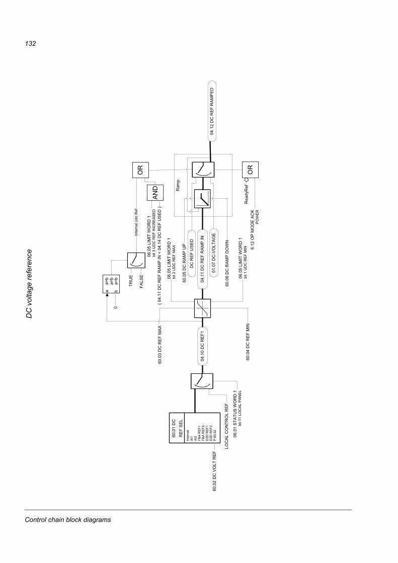
Control chain block diagrams
132
60
.04
DC
RE
F M
IN
04.1
1 D
C R
EF
RA
MP
IN
06.0
1 S
TA
TU
S W
OR
D 1
b
it 1
1 L
OC
AL P
AN
EL
60.0
3 D
C R
EF
MA
X
Ra
mp
04
.12
DC
RE
F R
AM
PE
D
Inte
rna
l
AI1
AI2
FB
A R
EF
1
FB
A R
EF
2
D2D
RE
F1
D2D
RE
F2
P.6
0.0
2
60.0
1 D
C
RE
F S
EL
60
.05
DC
RA
MP
UP
60.0
6 D
C R
AM
P D
OW
N
6.1
2 O
P M
OD
E A
CK
PO
WE
R
Read
yR
ef
01.0
7 D
C-V
OLT
AG
E6
0.0
2 D
C V
OL
T R
EF
04
.10
DC
RE
F1
LO
CA
L C
ON
TR
OL
RE
F
06.0
5 L
IMIT
WO
RD
1bit 3
UD
C R
EF
IN
CR
EA
SE
DA
ND
( 0
4.1
1 D
C R
EF
RA
MP
IN
< 0
4.1
4 D
C R
EF
US
ED
)
Inte
rnal U
dc R
ef
06
.05 L
IMIT
WO
RD
1bit 2
UD
C R
EF
MA
X
06
.05
LIM
IT W
OR
D 1
bit 1
UD
C R
EF
MIN
TR
UE
FA
LS
E
0
a b
a>
ba
=b
a<
b
OR
OR
DC
RE
F U
SE
D
DC
vol
tage
refe
renc
e

Control chain block diagrams
133
04
.20
Q P
OW
RE
F0
4.2
1 Q
PO
W R
AM
P I
N
Ra
mp
Q P
OW
RE
F U
SE
D
04
.22
Q P
OW
RE
F R
AM
PE
D
61
.05
Q P
OW
RA
MP
UP
61.0
6 Q
PO
W R
AM
P D
OW
N
ZE
RO
AI1
AI2
FB
A R
EF
1
FB
A R
EF
2
D2
D R
EF
1
D2
D R
EF
2
P.6
1.0
2
61
.01
Q P
OW
ER
RE
F S
EL
61
.03
Q P
OW
ER
RE
F M
AX
61
.04
Q P
OW
ER
RE
F M
IN
06
.05
LIM
IT W
OR
D 1
bit 5
Q P
OW
RE
F M
AX
06
.05
LIM
IT W
OR
D 1
bit 4
Q P
OW
RE
F M
IN
61
.02
Q P
OW
ER
RE
F
Re
ad
yR
ef
0
06
.05 L
IMIT
WO
RD
1bit 7
Q P
OW
NE
G L
IMA
ND
( 0
4.2
1 Q
PO
W R
AM
P I
N <
Q P
OW
RE
F U
SE
D )
06
.05
LIM
IT W
OR
D 1
bit 6
Q P
OW
PO
S L
IMA
ND
( 0
4.2
1 Q
PO
W R
AM
P I
N >
Q P
OW
RE
F U
SE
D )
OR
Rea
ctiv
e po
wer
refe
renc
e

Control chain block diagrams
134
ZE
RO
AI1
AI2
FB
A R
EF
1
FB
A R
EF
2
D2
D R
EF
1
D2
D R
EF
2
P.6
2.0
2
62
.01
PO
W
RE
F S
EL
LO
CA
L C
ON
TR
OL
LO
CA
L C
ON
TR
OL
RE
F
62
.03
MA
XIM
UM
PO
W R
EF
62
.04
MIN
IMU
M P
OW
RE
F
62
.05
PO
W R
AM
P U
P
62.0
6 P
OW
RA
MP
DO
WN
06
.05
LIM
IT W
OR
D 1
bit 1
1 P
OW
RE
F M
AX
06.0
5 L
IMIT
WO
RD
1b
it 1
0 P
OW
RE
F M
IN
04
.32
PO
W R
EF
RA
MP
ED
0
6.1
2 O
P M
OD
E A
CK
PO
WE
R
62.0
2 P
OW
ER
RE
F
04
.30
PO
W R
EF
1
Ra
mp
6.1
2 O
P M
OD
E A
CK
!=
PO
WE
R
OR
Rea
dyR
ef
0
04
.34
PO
WE
R R
EF
US
ED
04
.31
PO
W R
EF
RA
MP
IN
06
.05
LIM
IT W
OR
D 1
bit 8
PO
W M
IN L
IMA
ND
06
.05
LIM
IT W
OR
D 1
bit 9
PO
W M
AX
LIM
AN
D(
04.3
1 P
OW
RE
F R
AM
P I
N >
04
.34
PO
WE
R R
EF
US
ED
)
( 0
4.3
1 P
OW
RE
F R
AM
P I
N <
04
.34
PO
WE
R R
EF
US
ED
)
Pow
er re
fere
nce

Control chain block diagrams
135
DC
Ref In
it
01
.07
DC
-VO
LT
AG
E
04.1
2 D
C R
EF
RA
MP
ED
+-
Read
yR
ef
F(x
)4
0.0
4 V
OL
TA
GE
RE
SE
RV
EM
odula
tion I
nde
x R
ef
Mo
du
latio
n
ind
ex c
on
tro
ller
Mod
ula
tion I
ndex A
ct
+-
DC
CT
RL
RE
F I
N
Ud
c R
ef
Mo
d I
nd
ex
+
Kp
Ti
23
1.0
5 D
RO
OP
ING
RA
TE
Ma
xP
osV
alu
e
+
+
dt
Ud
c e
rr
x
6.1
2 O
P M
OD
E A
CK
PO
WE
R
0
64
.02
DC
CT
RL
DR
OO
P E
N
Ud
c R
ef
Dro
op
-1
PO
W R
EF
DC
CT
RL
TR
IG
6.1
2 O
P M
OD
E A
CK
DC
VO
LT
AG
E
DC
RE
F U
SE
D
01
.07
DC
-VO
LT
AG
E
60.0
3 D
C R
EF
MA
X
a b
a>
ba
=b
a<
bO
ve
r V
olta
ge
Ctr
l
Activa
tio
n L
imit
OV
_act
a b
a>
ba
=b
a<
bU
nd
er
Vo
lta
ge
Ctr
l
Activa
tio
n L
imit
UV
_act
60
.04
DC
RE
F M
IN
0
AN
D6
.12
OP
MO
DE
AC
KP
OW
ER
OV
_a
ct
AN
D6
.12
OP
MO
DE
AC
KP
OW
ER
UV
_a
ct
Ma
xN
eg
Va
lue0
06.0
5 L
IMIT
WO
RD
1bit 3
UD
C R
EF
IN
CR
EA
SE
D
Inte
rnal U
dc R
ef
DC
RE
F U
SE
D
DC
vol
tage
con
trol

Control chain block diagrams
136
01
.04
CU
RR
EN
T
01
.05
CU
RR
EN
T P
ER
C
01
.03
FR
EQ
UE
NC
Y
01
.07
DC
-VO
LT
AG
E
Q P
OW
RE
F U
SE
D
Ga
te s
igna
lsLin
e
syn
ch
ron
iza
tio
n
40
.02
SF
RE
FN
etw
ork
and
line
filt
er
mo
de
l
01
.22
IN
VE
RT
ER
PO
WE
R
US
ER
GR
ID D
AT
A:
63
.01
MA
INS
VO
LT
AG
E
63
.02
FR
EQ
UE
NC
Y
63.0
3 D
IRE
CT
ION
LIN
E F
ILT
DA
TA
:
23
1.0
6 L
LC
L C
ON
V
23
1.0
7 C
LC
L
23
1.0
8 L
LC
L G
RID
23
1.0
9 C
OR
E C
TR
L M
OD
E
Sw
itch
ing
fre
qu
en
cy r
ef
act
LC
L
04
.01
RE
AC
TIV
E P
OW
ER
+-
04
.22
Q P
OW
RE
F R
AM
PE
D
61
.04
Q P
OW
ER
RE
F M
IN
Re
active
po
we
r lim
ite
r
61
.03
Q P
OW
ER
RE
F M
AX
20
.08
TH
ER
M C
UR
LIM
20
.05
MA
XIM
UM
CU
RR
EN
T
04
.01
RE
AC
TIV
E P
OW
ER
01
.15
TE
MP
IN
VE
RT
ER
Sw
itch
ing
fre
qu
en
cy
limita
tio
n
04
.12
DC
RE
F R
AM
PE
D
04
.34
PO
WE
R R
EF
US
ED
62
.03
MA
XIM
UM
PO
W R
EF
62
.04
MIN
IMU
M P
OW
RE
F
Pow
er
limite
r
Re
active
po
we
r
co
ntr
olle
r
DC
vo
lta
ge
co
ntr
olle
r
+-
01
.07
DC
-VO
LT
AG
E
+
+P
OW
RE
F D
C C
TR
L
04
.32
PO
W R
EF
RA
MP
ED
Sta
rt
6.1
2 O
P M
OD
E A
CK
DC
VO
LT
AG
E
Read
yR
ef
Mo
du
latio
n I
nd
ex A
ct
DC
Ref In
it
06
.07
LC
LIM
ST
AT
US
bit 3
MA
XIM
UM
PO
WE
R
06
.07
LC
LIM
ST
AT
US
bit 2
MIN
IMU
M P
OW
ER
DT
C c
ore
06
.05
LIM
IT W
OR
D 1
bit 6
Q P
OW
PO
S L
IM
06
.05
LIM
IT W
OR
D 1
bit 7
Q P
OW
NE
G L
IM
No
te! A
rea
ma
rke
d w
ith
dash lin
e is h
andle
d a
s
reactive c
urr
ent
Reg
en s
uppl
y co
ntro
l

Appendix A – Fieldbus control
137
Appendix A – Fieldbus control
What this chapter containsThe chapter describes how the drive can be controlled by external devices over a communication network.
System overviewThe drive can be connected to a fieldbus controller via a fieldbus adapter module. The adapter module is connected to drive Slot 3.
The drive can be set to receive all of its control information through the fieldbus interface, or the control can be distributed between the fieldbus interface and other available sources, for example digital and analogue inputs.
The drive can communicate with fieldbus controller via fieldbus adapter using one of the following serial communication protocols:
– PROFIBUS-DP® (FPBA-01 adapter)– CANopen® (FCAN-01 adapter)– DeviceNet® (FDNA-01 adapter)– Modbus (FSCA-01 adapter).
Fieldbus
Otherdevices
Fieldbuscontroller
References
Data Flow
Status Word (SW)Actual values
Parameter R/W requests/responses
ACSM1
Slot 3
Process I/O (cyclic)
Service messages (acyclic)
Control Word (CW)
Fieldbus adapter
Fxxx
Process I/O (cyclic) or

Appendix A – Fieldbus control
138
Setting up communication through a fieldbus adapter moduleBefore configuring the drive for fieldbus control, the adapter module must be mechanically and electrically installed according to the instructions given in the User’s Manual of the appropriate fieldbus adapter module.
The communication between the drive and the fieldbus adapter module is activated by setting parameter 50.01 FBA ENABLE to (1) ENABLE. The adapter-specific parameters must also be set. See the table below.
Parameter Setting for fieldbus control Function/Information
COMMUNICATION INITIALIZATION AND SUPERVISION
50.01 FBA ENABLE (1) ENABLE Initializes communication between drive and fieldbus adapter module.
50.02 COMM LOSS FUNC
(0) NO(1) FAULT
Selects how the drive reacts in a fieldbus communication break.
50.03 COMM LOSS T OUT
0.3…6553.5 s Defines the time between communication break detection and the action selected with parameter 50.02 COMM LOSS FUNC.
50.04 FBA REF1 SCALE and 50.05 FBA REF2 SCALE
(0) RAW DATA(1) 100 = 1.00(2) 10 = 1.0
Defines the fieldbus reference and actual value scaling.
50.06 FBA ACT1 SEL and 50.07 FBA ACT2 SEL
(1073742087) DC VOLTAGE(1073742849) REACT. POWER(1073742102) ACTIVE POWER
Selects actual value signal.
ADAPTER MODULE CONFIGURATION
51.01 FBA TYPE – Displays the type of the fieldbus adapter module.51.02 FBA PAR2 These parameters are adapter module-specific. For more information, see the User’s Manual
of the fieldbus adapter module. Note that not all of these parameters are necessarily used.• • •51.26 FBA PAR2651.27 FBA PAR REFRESH
(0) DONE(1) REFRESH
Validates any changed adapter module configuration parameter settings.
51.28 PAR TABLE VER
– Displays the parameter table revision of the fieldbus adapter module mapping file stored in the memory of the drive.
51.29 DRIVE TYPE CODE
– Displays the drive type code of the fieldbus adapter module mapping file stored in the memory of the drive.
51.30 MAPPING FILE VER
– Displays the fieldbus adapter module mapping file revision stored in the memory of the drive.
51.31 D2FBA COMM STA
– Displays the status of the fieldbus adapter module communication.
51.32 FBA COMM SW VER
– Displays the common program revision of the adapter module.
51.33 FBA APPL SW VER
– Displays the application program revision of the adapter module.
Note: In the User’s Manual of the fieldbus adapter module, the parameter group number is 1 or A for parameters 51.01…51.26.

Appendix A – Fieldbus control
139
After the module configuration parameters have been set, the drive control parameters (see section Drive control parameters) must be checked and adjusted when necessary.
The new settings will take effect when the drive is powered up the next time (before powering off the drive, wait at least 1 minute), or when parameter 51.27 FBA PAR REFRESH is activated.
Drive control parametersThe Setting for fieldbus control column gives the value to use when the fieldbus interface is the desired source or destination for that particular signal. The Function/ Information column gives a description of the parameter.
TRANSMITTED DATA SELECTION
52.01 FBA DATA IN1 … 52.12 FBA DATA IN12
04…614…16101…9999
Defines the data transmitted from drive to fieldbus controller.Note: If the selected data is 32 bits long, two parameters are reserved for the transmission.
53.01 FBA DATA OUT1 … 53.12 FBA DATA OUT12
01…311…131001…9999
Defines the data transmitted from fieldbus controller to drive.Note: If the selected data is 32 bits long, two parameters are reserved for the transmission.
Note: In the User’s Manual of the fieldbus adapter module, the parameter group number is 3 or C for parameters 52.01…52.12 and 2 or B for parameters 53.01…53.12.
Parameter Setting for fieldbus control Function/Information
CONTROL COMMAND SOURCE SELECTION
10.01 EXT1 START FUNC
(3) FBA Selects fieldbus as the source for the start and stop commands when EXT1 is selected as the active control location.
10.04 EXT2 START FUNC
(3) FBA Selects fieldbus as the source for the start and stop commands when EXT2 is selected as the active control location.
60.01 DC REF SEL (1073742350) FBA REF1(1073742351) FBA REF2
Fieldbus reference REF1 or REF 2 is used as DC voltage reference.
61.01 Q POWER REF SEL
(1073742350) FBA REF1(1073742351) FBA REF2
Fieldbus reference REF1 or REF 2 is used as reactive power reference.
62.01 POW REF SEL (1073742350) FBA REF1(1073742351) FBA REF2
Fieldbus reference REF1 or REF 2 is used as active power reference.
SYSTEM CONTROL INPUTS
16.07 PARAM SAVE (0) DONE(1) SAVE
Saves parameter value changes (including those made through fieldbus control) to permanent memory.
Parameter Setting for fieldbus control Function/Information

Appendix A – Fieldbus control
140
The fieldbus control interfaceThe cyclic communication between a fieldbus system and the drive consists of 16/32-bit input and output data words. The drive supports at the maximum the use of 12 data words (16-bit) in each direction.
Data transmitted from the drive to the fieldbus controller is defined by parameters 52.01…52.12 (FBA DATA IN) and data transmitted from the fieldbus controller to the drive is defined by parameters 53.01…53.12 (FBA DATA OUT).
Fieldbus module
Fieldbus
Fieldbus network
specificinterface
DATAOUT 2)
4)123…12
DATAIN 2)
5)123…12
FBA MAIN SWFBA ACT1FBA ACT2
Par. 01.01…99.13
FBA MAIN CWFBA REF1FBA REF2
Par. 10.01…99.13
FBA profile
1) See also other parameters which can be controlled by the fieldbus.2) The maximum number of used data words is protocol-dependent.3) Profile/instance selection parameters. Fieldbus module specific parameters. For more information, see the
User’s Manual of the appropriate fieldbus adapter module.4) With DeviceNet the control part is transmitted directly.5) With DeviceNet the actual value part is transmitted directly.
Profileselect
3)
Profileselect
3)
Parameter table
10.01
EXT1/EXT2Start Func
/10.04
60.01/61.01
Referenceselector
/62.01
50.06
ACT1/ACT2Sel
/50.07
53.01/…/53.12
DATA OUTselect
52.01/…/52.12
DATA INselect
4)
5)
1)
Cyclic communication
Acyclic communicationSee the manual of the fieldbus adapter module.

Appendix A – Fieldbus control
141
The Control Word and the Status WordThe Control Word (CW) is the principal means of controlling the drive from a fieldbus system. The Control Word is sent by the fieldbus controller to the drive. The drive switches between its states according to the bit-coded instructions of the Control Word.
The Status Word (SW) is a word containing status information, sent by the drive to the fieldbus controller.
Actual valuesActual values (ACT) are 16/32-bit words containing information on selected operations of the drive.
FBA communication profileThe FBA communication profile is a state machine model which describes the general states and state transitions of the drive. The State diagram on page 143 presents the most important states (including the FBA profile state names). The FBA Control Word (2.12 FBA MAIN CW, page 32) commands the transitions between these states and the FBA Status Word (2.13 FBA MAIN SW, page 33) indicates the status of the drive.
Fieldbus adapter module profile (selected by adapter module parameter) defines how the control word and status word are transmitted in a system which consists of fieldbus controller, fieldbus adapter module and drive. With transparent modes, control word and status word are transmitted without any conversion between the fieldbus controller and the drive. With other profiles (e.g. PROFIdrive for FPBA-01, AC/DC drive for FDNA-01, DS-402 for FCAN-01 and ABB Drives profile for all fieldbus adapter modules) fieldbus adapter module converts the fieldbus-specific control word to the FBA communication profile and status word from FBA communication profile to the fieldbus-specific status word.
For descriptions of other profiles, see the User’s Manual of the appropriate fieldbus adapter module.
Note: The regen supply module does not support any fieldbus protocol specific profiles because they are intended for either speed/torque controlled drives or motion controlled drives. Use 16/32 transparent mode or ABB Drives profile instead.
Fieldbus referencesReferences and actual values are transmitted to/from the fieldbus controller as 16- or 32-bit integers depending on the selected profile. Internally, the firmware handles them as 32 signed integers (two’s complement). Therefore, scaling from 16- to 32-bit integers (and vice versa) may be needed. An internal integer value is denoted as a real value consisting of a sign bit, 15-bit integer value and 16-bit fractional value.
Transparent 32 mode
Values are transmitted to/from the fieldbus controller directly in the 32-bit internal data format without any scaling. A positive reference value (as real number) is

Appendix A – Fieldbus control
142
multiplied by 65536 to get the corresponding 32-bit integer value. A negative reference is formed by calculating the two’s complement from the corresponding positive reference value. Conversely, a 32-bit integer actual value must be divided by 65536 to get actual value as a real number.
For example, reference 1234.5 [SI unit] = 80904192 (= 1234.5 × 65536) as an integer and actual value 12345 (as integer) is approximately 0.18837 [SI unit] (= 12345 ÷ 65536).
Transparent 16 mode
Values are transmitted to/from the fieldbus controller as 16-bit integers. The fieldbus interface offers reference multiplier/actual value divisor for the transparent 16 mode as parameter T16 SCALE. Setting the scale to 65535 will provide practically exact approximation of 1 ~ 1.0 [SI unit]. Alternatively setting the scale to 6554 (accurate value would be 6553.6) will provide one decimal accuracy for a 16-bit integer.
Note: The value scaling works only with positive values. Correspondence between 16-bit and 32-bit negative values (two’s complements) is not so straightforward that it could be handled with one constant multiplier/divisor. Therefore, the use of transparent 16 is in practice limited to DC voltage control because DC voltage can get only positive values.
For example, if T16 SCALE = 65535, DC voltage as integer 615 ~ 614.99 V (= 65535 ÷ 65536 × 615).
When T16 SCALE = 6554, integer value 6155 ~ 615.54 V (= 6554 ÷ 65536 × 6155).
ABB Drives profile
The ABB Drives profile provides an easy way to transmit references and actual values as signed 16-bit integers via fieldbus. Basically, the ABB Drives profile is intended only for speed/torque controlled drives, but the same scaling principle normally used for speed/torque values can be used for any needed quantity (DC voltage [V], reactive power [kVAr] or active power [kW]).
Scaling is chosen with parameters 50.04 FBA REF1 SCALE and 50.05 FBA REF2 SCALE. They define whether the real value is given with one or two decimals’ accuracy as an integer, i.e. 10 = 1.0 [SI unit] or 100 = 1.00 [SI unit]. Usable scaling depends on the needed value range. One decimal’s accuracy provides value range -3276.8…+3276.7 [SI unit]. With two decimals, the value range is limited to -327.68…+327.67 [SI unit].

Appendix A – Fieldbus control
143
State diagramThe following presents the state diagram for the FBA communication profile. For other profiles, see the User’s Manual of the appropriate fieldbus adapter module.
MAINS OFF
Power ON
from any state
FBACommunication
Profile
(FBA SW Bit 0 = 1)
(FBA SW Bit 13 = 1)
(FBA SW Bit 6 = 1)
(FBA CW Bit 16 = 1)
(FBA CW Bit 0 = 1)
OFF1 (FBA CW Bit 4 = 1
OFF1ACTIVE
RUNNING (FBA SW Bit 3 = 1)
(FBA SW Bit 5 = 1)
from any state
from any state
Emergency StopOFF3 (FBA CW Bit 3 = 1
(FBA SW Bit 13 = 1)
OFF3ACTIVE
Emergency OFFOFF2 (FBA CW Bit 2 = 1
(FBA SW Bit 4 = 1)OFF2ACTIVE
FBA CW = Fieldbus Control WordFBA SW = Fieldbus Status Word
from any state
Fault
(FBA SW Bit 16 = 1)
(FBA CW Bit 8 = 1)
STARTINHIBITED
(FBA CW Bits 7 = 1)
READY TOSTART
Par. 10.12 = 0
from any state
and FBA CW Bit 0 = 1)
and FBA CW Bit 0 = 1)
and FBA CW Bit 0 = 1)
Par. 10.12 = 1
RUNDISABLEFAULT (FBA SW Bit 1 = 0)
(FBA CW Bit 7 = 0)
(FBA CW = xxxx xxxx xxxx xxx0 xxxx 1xxx 1xxx xx10)E
E

Appendix A – Fieldbus control
144

Appendix B – Drive-to-drive link
145
Appendix B – Drive-to-drive link
What this chapter containsThis chapter describes the wiring of, and available communication methods on the drive-to-drive link. Examples of using standard function blocks in the communication are also given starting on page 153.
GeneralThe drive-to-drive link is a daisy-chained RS-485 transmission line, constructed by connecting the X5 terminal blocks of the JCU Control Units of several drives. It is also possible to use an FMBA Modbus extension module installed into an option slot on the JCU. The firmware supports up to 63 nodes on the link.
The link has one master drive; the rest of the drives are followers. By default, the master broadcasts control commands as well as selected references for all followers. The master can send 8 messages per millisecond at 100/150-microsecond intervals. Sending one message takes approximately 15 microseconds, which results in a theoretical link capacity of roughly 6 messages per 100 microseconds.
Multicasting the control data and reference 1 to a pre-defined group of drives is possible, as is chained multicast messaging. Reference 2 is always broadcast by the master to all followers. See parameters 57.11…57.14.
WiringShielded twisted-pair cable (~100 ohm, e.g. PROFIBUS-compatible cable) must be used for the wiring. The maximum length of the link is 50 metres (164 ft).
The JCU Control Unit has a jumper (J3, “T”) next to the X5 terminal block for bus termination. Termination must be ON on the drives at the ends of the drive-to-drive link; on intermediate drives, termination must be OFF.
Instead of the X5 connector, an FMBA Modbus extension module can be used.
For best immunity, high quality cable is recommended. The cable should be kept as short as possible. Unnecessary loops and running the cable near power cables (such as motor cables) must be avoided.
Note: The cable shields are to be grounded to the control cable clamp plate on the drive. Follow the instructions given in the Hardware Manual of the drive.

Appendix B – Drive-to-drive link
146
The following diagram shows the wiring of the drive-to-drive link.
DatasetsDrive-to-drive communication uses DDCS (Distributed Drives Communication System) messages and dataset tables for data transfer. Each drive has a dataset table of 256 datasets, numbered 0…255. Each dataset contains 48 data bits. By default, datasets 0…15 and 200…255 are reserved for the drive firmware; datasets 16…199 are available for the user application program.
The contents of the standard communication datasets (16-bit control word and two 32-bit references) can be configured freely with pointer parameters and/or application programming with the DriveSPC tool. Depending on the drive control mode, the followers can be configured to use the drive-to-drive commands and references with the following parameters:
The communication status of the followers can be supervised by a periodic supervision message from the master to the individual followers (see parameters 57.04 FOLLOWER MASK 1 and 57.05 FOLLOWER MASK 2).
Drive-to-drive function blocks can be used in the DriveSPC tool to enable additional communication methods (such as follower-to-follower messaging) and to modify the use of datasets between the drives. See the function blocks in ACSM1 Speed and Torque Control Program Firmware Manual or ACSM1 Motion Control Program Firmware Manual.
Control data Parameter Setting for drive-to-drive communication
Start/Stop commands 10.01 EXT1 START FUNC10.04 EXT2 START FUNC (4) D2D
DC voltage reference 60.01 DC REF SEL (1073742355) D2D REF1 or(1073742356) D2D REF2
Reactive power reference 61.01 Q POWER REF SEL (1073742355) D2D REF1 or(1073742356) D2D REF2
Active power reference 62.01 POW REF SEL (1073742355) D2D REF1 or(1073742356) D2D REF2
X5:D2D
...
1
TJ3
Termination ON
JCUDrive 1
B
2A
3BG
ND
X5:D2D
1
J3
Termination OFF
JCUDrive 2
B
2A
3BG
NDT
X5:D2D
1
TJ3
Termination ON
JCUDrive n
B
2A
3BG
ND

Appendix B – Drive-to-drive link
147
Types of messagingEach drive on the link has a unique node address allowing point-to-point communication between two drives. The node address 0 is automatically assigned to the master drive; on other drives, the node address is defined by parameter 57.03 NODE ADDRESS.
Multicast addressing is supported, allowing the composition of groups of drives. Data sent to a multicast address is received by all drives that have that address. A multicast group can consist of 1…62 drives.
In broadcast messaging, data can be sent to all drives (actually, all followers) on the link.
Both master-to-follower(s) and follower-to-follower(s) communication is supported. A follower can send one message to another follower (or a group of followers) after receiving a token message from the master.
Type of messaging NotePoint-to-point Master point-to-point Supported only at master
Read remote Supported only at master
Follower point-to-point Supported only at followers
Standard multicast For both master and followers
Broadcast For both master and followers
Token message for follower-to-follower communication –
Chained multicast Supported only for drive-to-drive reference 1 and command word.

Appendix B – Drive-to-drive link
148
Master point-to-point messaging (read and write)In this type of messaging, the master sends one dataset (LocalDsNr) from its own dataset table to the follower’s. TargetNode stands for the node address of the follower; RemoteDsNr specifies the target dataset number.
The follower responds by returning the contents of the next dataset. The response is stored into dataset LocalDsNr+1 in the master.
Note: Master point-to-point messaging is only supported at the master because the response is always sent to node address 0 (the master).
Read remote messaging (read only)The master can read a dataset (RemoteDsNr) from a follower specified by TargetNode. The follower returns the contents of the requested dataset to the master. The response is stored at dataset LocalDsNr in the master.
Note: Read remote messaging is only supported at the master because the response is always sent to node address 0 (the master).
Master
Dataset table
(LocalDsNr)(LocalDsNr+1)
TargetNode = X
57.03 NODE ADDRESS = X
Follower
Dataset table
(RemoteDsNr)(RemoteDsNr+1)
Master
Dataset table
(LocalDsNr)TargetNode = X
57.03 NODE ADDRESS = X
Follower
Dataset table
(RemoteDsNr)

Appendix B – Drive-to-drive link
149
Follower point-to-point messaging (write only)This type of messaging is for point-to-point communication between followers. After receiving a token from the master, a follower can send one dataset to another follower with a follower point-to-point message. The target drive is specified using the node address.
Note: The data is not sent to the master.
Standard multicast messaging (write only)In standard multicast messaging, one dataset can be sent to a group of drives having the same standard multicast group address. The target group is defined by the D2D_Conf standard function block.
The sending drive can either be the master, or a follower after receiving a token from the master.
Note: The master does not receive the sent data even if it is a member of the target multicast group.
Follower
Dataset table
(LocalDsNr)TargetNode = X
57.03 NODE ADDRESS = X
Follower
Dataset table
(RemoteDsNr)
Master
Dataset table
Token
Follower
Dataset table
(RemoteDsNr)
Target Grp = X
Std Mcast Group = X
Follower
Dataset table
(RemoteDsNr)
Master
Dataset table
(LocalDsNr)
Master-to-follower(s) multicasting
Std Mcast Group = X

Appendix B – Drive-to-drive link
150
Broadcast messaging (write only)In broadcasting, the master sends one dataset to all followers, or a follower sends one dataset to all other followers after receiving a token from the master.
The target (Target Grp) is automatically set to 255 denoting all followers.
Note: The master does not receive any data broadcast by the followers.
Follower
Dataset table
(RemoteDsNr)
Target Grp = X
Std Mcast Group = X
Follower
Dataset table
(RemoteDsNr)
Master
Dataset table
Follower-to-follower(s) multicasting
Std Mcast Group = X
Follower
Dataset table
(LocalDsNr)
Token
Follower
Dataset table
(RemoteDsNr)
Target Grp = 255
Follower
Dataset table
(RemoteDsNr)
Master
Dataset table
(LocalDsNr)
Master-to-follower(s) broadcasting

Appendix B – Drive-to-drive link
151
Chained multicast messagingChained multicasting is supported only for drive-to-drive reference 1 by the firmware.
The message chain is always started by the master. The target group is defined by parameter 57.13 NEXT REF1 MC GRP. The message is received by all followers that have parameter 57.12 REF1 MC GROUP set to the same value as parameter 57.13 NEXT REF1 MC GRP in the master.
If a follower have parameters 57.03 NODE ADDRESS and 57.12 REF1 MC GROUP set to the same value, it becomes a submaster. Immediately after a submaster receives the multicast message, it sends its own message to the next multicast group defined by parameter 57.13 NEXT REF1 MC GRP.
The duration of the entire message chain is approximately 15 microseconds multiplied by the number of links in the chain (defined by parameter 57.14 NR REF1 MC GRPS in the master).
Follower
Dataset table
(RemoteDsNr)
Target Grp = 255
Follower
Dataset table
(RemoteDsNr)
Master
Dataset table
Follower-to-follower(s) broadcasting
Follower
Dataset table
(LocalDsNr)
Token
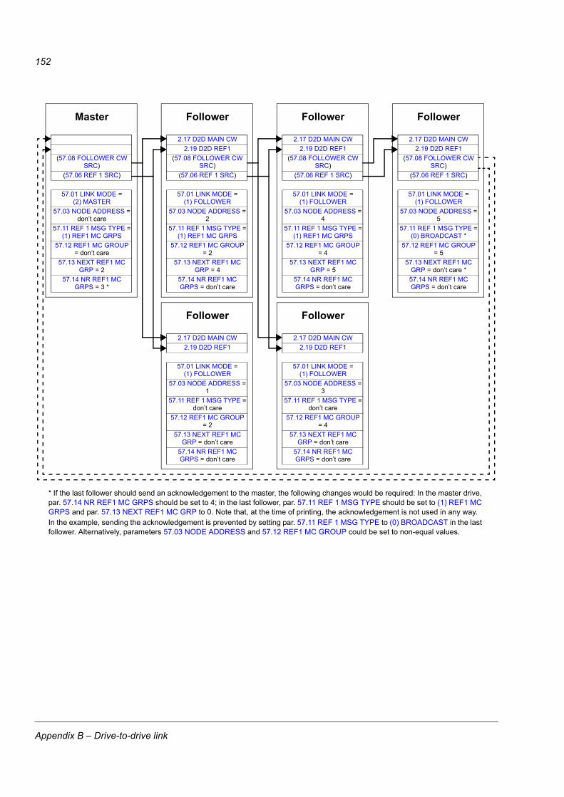
Appendix B – Drive-to-drive link
152
Master
(57.08 FOLLOWER CW SRC)
(57.06 REF 1 SRC)
57.01 LINK MODE =(2) MASTER
57.03 NODE ADDRESS =don’t care
57.11 REF 1 MSG TYPE =(1) REF1 MC GRPS
57.12 REF1 MC GROUP = don’t care
57.13 NEXT REF1 MC GRP = 2
57.14 NR REF1 MC GRPS = 3 *
Follower
2.17 D2D MAIN CW2.19 D2D REF1
57.01 LINK MODE =(1) FOLLOWER
57.03 NODE ADDRESS =1
57.11 REF 1 MSG TYPE =don’t care
57.12 REF1 MC GROUP = 2
57.13 NEXT REF1 MC GRP = don’t care
57.14 NR REF1 MC GRPS = don’t care
Follower
2.17 D2D MAIN CW2.19 D2D REF1
(57.08 FOLLOWER CW SRC)
(57.06 REF 1 SRC)
57.01 LINK MODE =(1) FOLLOWER
57.03 NODE ADDRESS =2
57.11 REF 1 MSG TYPE =(1) REF1 MC GRPS
57.12 REF1 MC GROUP = 2
57.13 NEXT REF1 MC GRP = 4
57.14 NR REF1 MC GRPS = don’t care
Follower
2.17 D2D MAIN CW2.19 D2D REF1
57.01 LINK MODE =(1) FOLLOWER
57.03 NODE ADDRESS =3
57.11 REF 1 MSG TYPE =don’t care
57.12 REF1 MC GROUP = 4
57.13 NEXT REF1 MC GRP = don’t care
57.14 NR REF1 MC GRPS = don’t care
Follower
2.17 D2D MAIN CW2.19 D2D REF1
(57.08 FOLLOWER CW SRC)
(57.06 REF 1 SRC)
57.01 LINK MODE =(1) FOLLOWER
57.03 NODE ADDRESS =4
57.11 REF 1 MSG TYPE =(1) REF1 MC GRPS
57.12 REF1 MC GROUP = 4
57.13 NEXT REF1 MC GRP = 5
57.14 NR REF1 MC GRPS = don’t care
Follower
2.17 D2D MAIN CW2.19 D2D REF1
(57.08 FOLLOWER CW SRC)
(57.06 REF 1 SRC)
57.01 LINK MODE =(1) FOLLOWER
57.03 NODE ADDRESS =5
57.11 REF 1 MSG TYPE =(0) BROADCAST *
57.12 REF1 MC GROUP = 5
57.13 NEXT REF1 MC GRP = don’t care *57.14 NR REF1 MC GRPS = don’t care
* If the last follower should send an acknowledgement to the master, the following changes would be required: In the master drive, par. 57.14 NR REF1 MC GRPS should be set to 4; in the last follower, par. 57.11 REF 1 MSG TYPE should be set to (1) REF1 MC GRPS and par. 57.13 NEXT REF1 MC GRP to 0. Note that, at the time of printing, the acknowledgement is not used in any way.In the example, sending the acknowledgement is prevented by setting par. 57.11 REF 1 MSG TYPE to (0) BROADCAST in the last follower. Alternatively, parameters 57.03 NODE ADDRESS and 57.12 REF1 MC GROUP could be set to non-equal values.

Appendix B – Drive-to-drive link
153
Examples of using standard function blocks in drive-to-drive communication
See also the descriptions of the drive-to-drive function blocks in ACSM1 Speed and Torque Control Program Firmware Manual or ACSM1 Motion Control Program Firmware Manual.
Example of master point-to-point messaging
Master Follower (node 1)
1. The master sends a constant (1) and the value of the message counter into follower dataset 20. Data is prepared to and sent from dataset 16.
2. The follower sends the received counter value and a constant (21) as a reply to the master.
3. The master calculates the difference of the latest message number and received data.

Appendix B – Drive-to-drive link
154
Example of read remote messaging
Releasing tokens for follower-to-follower communication
Master Follower (node 1)
1. The master reads the contents of the follower dataset 22 into its own dataset 18. Data is accessed using the DS_ReadLocal block.
2. In the follower, constant data is prepared into dataset 22.
Master
1. This drive-to-drive link consists of three drives (master and two followers).
2. The master operates as a “chairman”. Follower 1 (node 1) is allowed to send one message every 3 milliseconds. Follower 2 (node 2) is allowed to send one message every 6 milliseconds.

Appendix B – Drive-to-drive link
155
Example of follower point-to-point messaging
Follower 1 Follower 2
1. Follower 1 writes local dataset 24 to follower 2 dataset 30 (3 ms interval).2. Follower 2 writes local dataset 33 to follower 1 dataset 28 (6 ms interval).3. In addition, both followers read received data from local datasets.
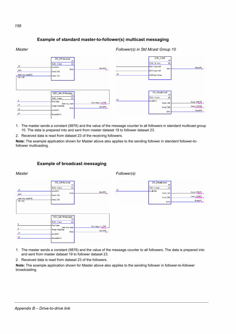
Appendix B – Drive-to-drive link
156
Example of standard master-to-follower(s) multicast messaging
Example of broadcast messaging
Master Follower(s) in Std Mcast Group 10
1. The master sends a constant (9876) and the value of the message counter to all followers in standard multicast group 10. The data is prepared into and sent from master dataset 19 to follower dataset 23.
2. Received data is read from dataset 23 of the receiving followers.Note: The example application shown for Master above also applies to the sending follower in standard follower-to-follower multicasting.
Master Follower(s)
1. The master sends a constant (9876) and the value of the message counter to all followers. The data is prepared into and sent from master dataset 19 to follower dataset 23.
2. Received data is read from dataset 23 of the followers.Note: The example application shown for Master above also applies to the sending follower in follower-to-follower broadcasting.

157

158

3AU
A00
0005
2174
Rev
A /
EN
EFF
EC
TIV
E: 2
009-
12-1
1
ABB OyAC DrivesP.O. Box 184FI-00381 HELSINKIFINLANDTelephone +358 10 22 11Fax +358 10 22 22681Internet http://www.abb.com
ABB Inc.Automation TechnologiesDrives & Motors16250 West Glendale DriveNew Berlin, WI 53151USATelephone 262 785-3200
800-HELP-365Fax 262 780-5135
ABB Beijing Drive Systems Co. Ltd.No. 1, Block D, A-10 Jiuxianqiao BeiluChaoyang DistrictBeijing, P.R. China, 100015Telephone +86 10 5821 7788Fax +86 10 5821 7618Internet http://www.abb.com