flash adc design - weeblykylelichtenberg.weebly.com/uploads/1/1/9/5/11959867/adc_final.pdf · iowa...
TRANSCRIPT

Iowa State University: Department of Electrical Engineering EE 435: Flash ADC Design
1
FLASH ADC DESIGN Iowa State University
Dr. Degang Chen
May 5, 2013
Xing Cao
Greg Bulleit
Kyle Lichtenberg
Ang Lu

Iowa State University: Department of Electrical Engineering EE 435: Flash ADC Design
2
TABLE OF CONTENTS
Abstract ......................................................................................................................................................................... 3
Introduction ................................................................................................................................................................... 3
Circuit Design ................................................................................................................................................................. 3
Comparator ............................................................................................................................................................... 3
Preamp .................................................................................................................................................................. 4
Latch ...................................................................................................................................................................... 5
Comparator Simulation ......................................................................................................................................... 6
R-String ...................................................................................................................................................................... 6
Encoder ..................................................................................................................................................................... 7
Encoder Design Procedure .................................................................................................................................... 7
Truth Table ............................................................................................................................................................ 8
NAND Gate and NOR Gate .................................................................................................................................. 10
Encoder Structure ............................................................................................................................................... 11
Simulation of the Encoder .................................................................................................................................. 13
D Flip Flop ................................................................................................................................................................ 14
Structure ............................................................................................................................................................. 14
D Flip Flop Simulation ......................................................................................................................................... 15
Test Bench & Simulation .............................................................................................................................................. 15
Beginning Test Simulations ..................................................................................................................................... 15
Strobe Simulations .................................................................................................................................................. 16
Linearity .............................................................................................................................................................. 16
Converter Dynamic Performance ....................................................................................................................... 17
Conclusion ................................................................................................................................................................... 18
Appendix I: Matlab Linearity Code .............................................................................................................................. 19
APPendix II: Matlab Dynamic Performance Code ........................................................................................................ 20

Iowa State University: Department of Electrical Engineering EE 435: Flash ADC Design
3
ABSTRACT
ADC’s are an important structure used in all digital applications that require analog inputs, outputs, or both. Flash
ADC’s are used for very high speed applications, but are not as accurate as other ADC architectures. Another
obstacle when designing a flash ADC is the power consumption, since a large number of comparators is needed.
This also takes up a large area, especially for flash ADC that are clocked very fast (Carusone, Johns, Martin).
INTRODUCTION
In this project we were confronted with the task of designing a 6 bit flash ADC. Approaching the project we knew
that an r-string stage, comparator array, and encoder were needed. Along with this, many specifications and
parameter requirements had to be met.
CIRCUIT DESIGN
In this section of the report, the components of the circuit are discussed. All sections are broken down to the most
elementary of components in order to discuss their operation accurately. Simulations are also run for each
component in order to provide a brief glance at their accuracy before looking at the circuit as a whole.
COMPARATOR
The first step in the design of the flash ADC and most important component was the comparator. The comparator
consisted of two main stages, the preamp and the latch. The circuit in its entirety is shown below:
Figure 1: Full Comparator Schematic

Iowa State University: Department of Electrical Engineering EE 435: Flash ADC Design
4
PREAMP
The preamp consisted of a single stage with a differential input. NMOS transistors were chosen in order to achieve
a higher gain with smaller input transistors. The preamp used resistors instead of diode-connected transistors in
order to increase the input range to VDD. This larger input range allowed us to use a larger signal input, while its
low gain helped to increase the overall speed of the comparator. The low gain also increased the unity gain
frequency greatly to around 1GHz. The preamp schematic is as follows:
Figure 2: Preamp Circuit for Comparator
The preamp had a tail current of 337.3 µA when simulated, resulting in a total power of 108 mW since there are 64
total preamps in the ADC. The gain was 20 dB, and the GB is fairly high, as displayed in the following plot:

Iowa State University: Department of Electrical Engineering EE 435: Flash ADC Design
5
Figure 3: Preamp Gain
LATCH
The latch was designed to operate at high speeds along with the preamp. The latch design came from “A CMOS 8-
Bit High-Speed A/D Converter IC” (IEEE 1985). This latch design allowed us to use minimum sized devices to
increase the speed of the latch operation. The latch operates by resetting and tracking when the clock is high, and
latching when the clock is low. Inverters are included in the latch stage in order to act as a buffer between the
latch and the output circuitry. The inverters can be cascaded to allow this latch to drive much larger digital circuits.
In our case, the inverter size did not have to be increased since we were outputting to a minimal number of
devices. The latch stage of the comparator consumed tens of nano amps when not latched, and 136.3 µA when
latched. This resulted in an average power of 21.8 mW when accounting for all 64 latches. The latch circuit is as
follows:
Figure 4: Latch Circuit for Comparator

Iowa State University: Department of Electrical Engineering EE 435: Flash ADC Design
6
COMPARATOR SIMULATION
In order to ensure the comparator was working properly, a simple simulation was run with a ramp input. The
reference voltage given to the circuit was 2.5 V, and the input ramped up to a maximum of 5 volts. The following
plot displays the operation of the comparator, and how the output is cut off once the input voltage is higher than
that of the reference voltage.
Figure 5: Ramp Comparator Simulation
After testing each individual part of the comparator, it could be concluded that the analog circuitry of our ADC
consumes roughly 129.8 mW of power. This number is far below the given rating of 450 mW of power, and gives
us plenty of leeway when the digital circuitry is switching, and also the power consumed by the r-string.
R-STRING
The r-string of the ADC was used to divide the reference voltage equally between the comparators. This was done
using a total of 65 resistors, the top and bottom resistors having a value of 1.5 Ohms, and the remaining 63 having
a value of 3 Ohms. This value of resistance was chosen in order to increase the power footprint to a level suitable
to that of the circuit. The power could not be too high however, or the power specifications could not be met.
After running a simulation on the power consumption of the r-string, it was concluded that 63.8 mW of power was
consumed. The voltage across the 1.5 Ohm resistors was 27.34 mV, and the voltage across the remaining resistors
that fed into the comparators was 54.69 mV. The entire r-string configuration had a current of 18.23 mA. A screen
shot of the configuration used, along with their input to the comparators is shown in Figure 6:

Iowa State University: Department of Electrical Engineering EE 435: Flash ADC Design
7
Figure 6: Four Resistors of the R-String (Seen on Left)
After testing the entire analog portion of our circuitry, the total average power consumption was 193.6 mW of
power, with a worst case scenario power consumption of 215 mW (the worst case being that all latches in the all
of the comparators are on and latching).
ENCODER
In order to interpret the thermal code that was generated from the comparator string, a thermometer to binary
encoder was necessary to generate the final ADC output. The logic function, the design of the circuit, transistor
level implementation, and simulation of the thermal to binary encoder is presented. Also, to make sure that the
outputs are correctly interpreted by following digital logic, a d flip flop is used, and will be talked about later.
ENCODER DESIGN PROCEDURE
According to the full ADC structure from our textbook, the thermal to binary encoder is being built after the
comparator string. It includes a two input NAND gate and an encoder. Based on our requirement, we built an
encoder which has 63 inputs and 6 outputs.

Iowa State University: Department of Electrical Engineering EE 435: Flash ADC Design
8
Figure 7: Flash ADC Architecture (Carusone, Johns, Martin)
TRUTH TABLE
B<5:0 Thermal code from A62A0
000000 1111111111111111111111111111111111111111111111111111111111111111
000001 1111111111111111111111111111111111111111111111111111111111111110
000010 1111111111111111111111111111111111111111111111111111111111111101
000011 1111111111111111111111111111111111111111111111111111111111111011
000100 1111111111111111111111111111111111111111111111111111111111110111
000111 1111111111111111111111111111111111111111111111111111111111101111
000110 1111111111111111111111111111111111111111111111111111111111011111
000101 1111111111111111111111111111111111111111111111111111111110111111
001000 1111111111111111111111111111111111111111111111111111111101111111
001011 1111111111111111111111111111111111111111111111111111111011111111

Iowa State University: Department of Electrical Engineering EE 435: Flash ADC Design
9
001010 1111111111111111111111111111111111111111111111111111110111111111
001001 1111111111111111111111111111111111111111111111111111101111111111
001100 1111111111111111111111111111111111111111111111111111011111111111
001111 1111111111111111111111111111111111111111111111111110111111111111
001110 1111111111111111111111111111111111111111111111111101111111111111
001101 1111111111111111111111111111111111111111111111111011111111111111
… …
… …
111100 1110111111111111111111111111111111111111111111111111111111111111
111101 1101111111111111111111111111111111111111111111111111111111111111
111110 1011111111111111111111111111111111111111111111111111111111111111
111111 0111111111111111111111111111111111111111111111111111111111111111
Table 1: Truth Table for Encoder
From the truth table, we obtained following logic function:
0 0 2 4 6 8 10 12 14 16 18 20 22 24 26 28 30 32 34 36 38 40 42 44 46 48 50 52 54 56 58 60 62
1 1 2 5 6 9 10 13 14 17 18 21 22 25 26 29 30 33 34 37
b a a a a a a a a a a a a a a a a a a a a a a a a a a a a a a a a
b a a a a a a a a a a a a a a a a a a a a
38 41 42 45 46 49 50 53 54 57 58 61 62
2 3 4 5 6 11 12 13 14 19 20 21 22 27 28 29 30 35 36 37 38 43 44 45 46 51 52 53 54 59 60 61 62
3 7 8 9 10 11 12
a a a a a a a a a a a a
b a a a a a a a a a a a a a a a a a a a a a a a a a a a a a a a a
b a a a a a a
13 14 23 24 25 26 27 28 29 30 39 40 41 42 43 44 45 46 55 56 57 58 59 60 61 62
4 15 16 17 18 19 20 21 22 23 24 25 26 27 28 29 30 47 48 49 50 51 52 53 5
a a a a a a a a a a a a a a a a a a a a a a a a a a
b a a a a a a a a a a a a a a a a a a a a a a a a
4 55 56 57 58 59 60 61 62
5 31 32 33 34 35 36 37 38 39 40 41 42 43 44 45 46 47 48 49 50 51 52 53 54 55 56 57 58 59 60 61 62
a a a a a a a a
b a a a a a a a a a a a a a a a a a a a a a a a a a a a a a a a a
Figure 8: Derived Logic Function

Iowa State University: Department of Electrical Engineering EE 435: Flash ADC Design
10
From the logic function, it was obvious that we needed NAND gates and NOR gates. We used the following
components in this order: 16 two-input NAND gates, 8 two-input NOR gates, 4 two-input NAND gates, 2 two-input
NOR gates and 1 two-input NAND gate.
NAND GATE AND NOR GATE
The following figures display the structure and size of NAND gate and NOR gate:
Figure 9: Two-Input NAND Gate Schematic Figure 10: Two-Input NOR Gate Schematic
Figure 11: Schematic of the two-input NAND Gate with an Inverter in One of the Inputs

Iowa State University: Department of Electrical Engineering EE 435: Flash ADC Design
11
ENCODER STRUCTURE
First, we used the NAND gates and NOR gates to build a 1 bit encoder by applying the logic function.
Figure 12: One Bit Encoder Structure

Iowa State University: Department of Electrical Engineering EE 435: Flash ADC Design
12
Next, we built 6 one-bit encoders to achieve the 63 inputs.
Figure 13: 63 to 6 Encoder Structure
Figure 14: Final Encoder Structure

Iowa State University: Department of Electrical Engineering EE 435: Flash ADC Design
13
SIMULATION OF THE ENCODER
The following figure shows the test bench of the encoder. The thermometer code is generated by 64 pulse voltage
sources and its complement code is generated by inverters after the 64 pulse voltage sources.
Figure 15: Encoder Test Bench
Pulse width of each of input of encoder increase by a time period of 1.2ns.
Figure 16: First Six Positive Outputs of the Comparator

Iowa State University: Department of Electrical Engineering EE 435: Flash ADC Design
14
D FLIP FLOP
STRUCTURE
The final stage of our flash ADC was to design and implement a d flip flop. The purpose of the d flip flop is to hold
the value of the digital logic in order to decrease the amount of error received. This value is then reset at the low
point of each clock cycle, and once high again, the input is written into the d flip flop. We used the following
structure for our d flip flop:
Figure 18: D Flip Flop Schematic
Figure 17: Output Response of the Encoder
Iowa State University: Department of Electrical Engineering EE 435: Flash ADC Design
15
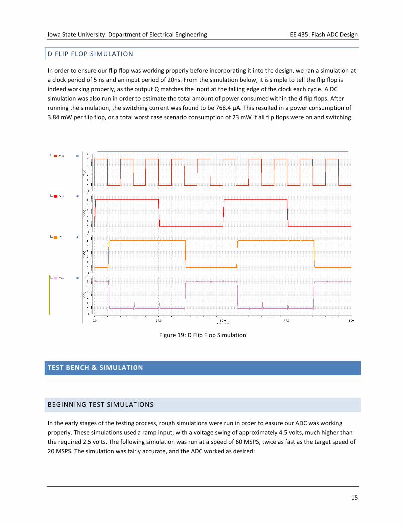
D FLIP FLOP SIMULATION
In order to ensure our flip flop was working properly before incorporating it into the design, we ran a simulation at
a clock period of 5 ns and an input period of 20ns. From the simulation below, it is simple to tell the flip flop is
indeed working properly, as the output Q matches the input at the falling edge of the clock each cycle. A DC
simulation was also run in order to estimate the total amount of power consumed within the d flip flops. After
running the simulation, the switching current was found to be 768.4 µA. This resulted in a power consumption of
3.84 mW per flip flop, or a total worst case scenario consumption of 23 mW if all flip flops were on and switching.
Figure 19: D Flip Flop Simulation
TEST BENCH & SIMULATION
BEGINNING TEST SIMULATIONS
In the early stages of the testing process, rough simulations were run in order to ensure our ADC was working
properly. These simulations used a ramp input, with a voltage swing of approximately 4.5 volts, much higher than
the required 2.5 volts. The following simulation was run at a speed of 60 MSPS, twice as fast as the target speed of
20 MSPS. The simulation was fairly accurate, and the ADC worked as desired:

Iowa State University: Department of Electrical Engineering EE 435: Flash ADC Design
16
Figure 20: Early Ramp Test of Entire Circuit
STROBE SIMULATIONS
LINEARITY
Once the circuit was complete, strobe simulations were then run in Cadence. The data from these simulations
were then fed into Matlab in order to perform operations to obtain the desired parameters. After running the
code, the following plot was obtained, which outlines the linearity of the ADC (all Matlab code for this portion of
the report is included in Appendix I):
Figure 21: Matlab Plot of Linearity

Iowa State University: Department of Electrical Engineering EE 435: Flash ADC Design
17
From this Matlab function, we obtained the following values:
DNL 0.2928 LSB
INL 2.2471 LSB
Gain Error -24.892 LSB
VOffset 0.1473 LSB
Table 2: ADC Parameters
CONVERTER DYNAMIC PERFORMANCE
After extracting the basic parameters, the data was then fed into Matlab once again in order to determine the FFT
of the flash ADC. The data was run for the ADC at many levels set off of the Nyquist rate, and the following plots
and output data was obtained (all Matlab code used to obtain the FFT is included in Appendix II of the report):
Figure 22: FFT at Near Nyquist Figure 23: FFT at 5% Nyquist
Frequency (MHz) SINAD SNR THD SFDR ENOB
30.306 8.4249 8.4249 - 14.0885 1.1071
8.333 22.7249 23.128 -22.7249 24.8682 3.4825
1.668 32.2769 33.2769 -40.4778 42.7262 5.1096
IDEAL 39.21 39.21 - - 6.22
Table 3: Dynamic Performance Data

Iowa State University: Department of Electrical Engineering EE 435: Flash ADC Design
18
CONCLUSION
After much time and effort, a successful flash ADC was designed and built. At times, our ADC did not perform as
well as desired, but none the less worked in a fairly accurate and efficient manner. We were under our power
requirements, and more than tripled our frequency requirements. By increasing the frequency to a much higher
point, we may have negatively impacted the performance of the ADC. This project required us to apply all that we
have learned throughout the course, and also go beyond the scope of the class for the digital applications.

Iowa State University: Department of Electrical Engineering EE 435: Flash ADC Design
19
APPENDIX I: MATLAB LINEARITY CODE
function [Vos,Gerror,DNLk,INLk,binWidth,DNL,INL,mono_flag] =
ADClinearity(Vrefp,Vrefn,Cout,Vtran)
idealLSB = (Vrefp-Vrefn)/length(Cout);
Vos = (Vtran(1)-(Vrefn+0.5*idealLSB))/idealLSB;
for k = 1:(max(Cout)-1)
binWidth(k) = Vtran(k+1)-Vtran(k);
end
actualLSB = sum(binWidth)/length(binWidth);
Gerror = ((Vtran(length(Vtran))-Vtran(1))-(Vrefp-2*actualLSB))/idealLSB;
for k = 1:(max(Cout)-1)
DNLk(k) = binWidth(k)/actualLSB-1;
end
INLk(1)=DNLk(1);
for k = 2:(max(Cout)-1)
INLk(k) = INLk(k-1)+DNLk(k);
end
DNL =max(DNLk);
INL =max(abs(INLk))-Vos;
mono_flag = 'monotonic';
for k = 1:(max(Cout)-2)
if (Vtran(k+1)-Vtran(k))<0
mono_flag = 'non-monotonic';
else
end
end

Iowa State University: Department of Electrical Engineering EE 435: Flash ADC Design
20
APPENDIX II: MATLAB DYNAMIC PERFORMANCE CODE
[time6, D6, time5, D5, time4, D4, time3, D3, time2, D2, time1, D1] =
textread('nyquist2.csv','%n%n%n%n%n%n%n%n%n%n%n%n%*[^\n]','delimiter',',');
D = [D1,D2,D3,D4,D5,D6];
for n=1:length(D1)
for k=1:6
if D(n,k) < 2.5
D(n,k) = 0;
else
D(n,k) = 1;
end
end
end
aOut = bi2de(D);
%aOut = bi2de(D,2,'left-msb');
bits = 6;
numSamp = length(aOut);
freClk = 1/15E-9;
maxDB = 20*log10(max(aOut/2^bits));
Dout = aOut-mean(aOut);
Dout = Dout/2^bits;
winDout = Dout;
winDout = winDout/numSamp;
fftDout = fft(winDout,numSamp);
dBfftDout = 20*log10(abs(fftDout));
figure;

Iowa State University: Department of Electrical Engineering EE 435: Flash ADC Design
21
[maxDB,index] = max(dBfftDout(6:numSamp/2));
index=index+5;
plot([0:numSamp/2-1].*freClk/numSamp/1E6,dBfftDout(1:numSamp/2)-maxDB-6);
grid on;
title('FFT 5% Nyquist');
xlabel('Analog Input Frequincy(MHz)');
ylabel('Amplitude(dB)');
span = 5;
spanH = 5;
spectPow = abs(fftDout).*(abs(fftDout));
spectPow(1)=0;
powDC = sum(spectPow(1:span));
powSig = sum(spectPow(index-span:index+span));
FreH = [];
PowH = [];
for n = 1:8
hTone = (n*(index-1)+1)/numSamp;
if hTone <= .5
FreH = [FreH hTone];
hPeak = max(spectPow(round(hTone*numSamp)-spanH:round(hTone*numSamp)+spanH));
hBin = find(spectPow(round(hTone*numSamp)-spanH:round(hTone*numSamp)+spanH) ==
hPeak);
hBin = hBin + round(hTone*numSamp)-spanH-1;
PowH = [PowH sum(spectPow(hBin-1:hBin+1))];
end
end
PowDistortion = sum(PowH(1:length(PowH)))- PowH(1);
PowNoise = sum(spectPow(1:numSamp/2))-powDC-powSig-PowDistortion;

Iowa State University: Department of Electrical Engineering EE 435: Flash ADC Design
22
InputFrequincy = (index-1)/numSamp*freClk
Amplitude = (max(aOut)-min(aOut))/2^bits
AmplitudedB = 20*log10(Amplitude)
SINAD = 10*log10(powSig/(PowNoise+PowDistortion))
SNR = 10*log10(powSig/PowNoise)
THD = 10*log10(PowDistortion/PowH(1))
DoutTemp = dBfftDout;
DoutTemp(1:span)=-90;
DoutTemp(index-span:index+span)=-90;
[maxdf,fd] = max(DoutTemp(1:numSamp/2));
SFDR = 10*log10(PowH(1)/max(PowH(2:8)))
ENOB = (SINAD-1.76)/6.02