flash memory trends - forward-insights.com memory trends_fms2.pdf · • scaling challenges vendors...
TRANSCRIPT

Santa Clara, CA USA
August 2008 1
Flash Memory Trends
Gregory Wong, Founder and Principal Analyst
Santa Clara, CA USA
August 2008 2
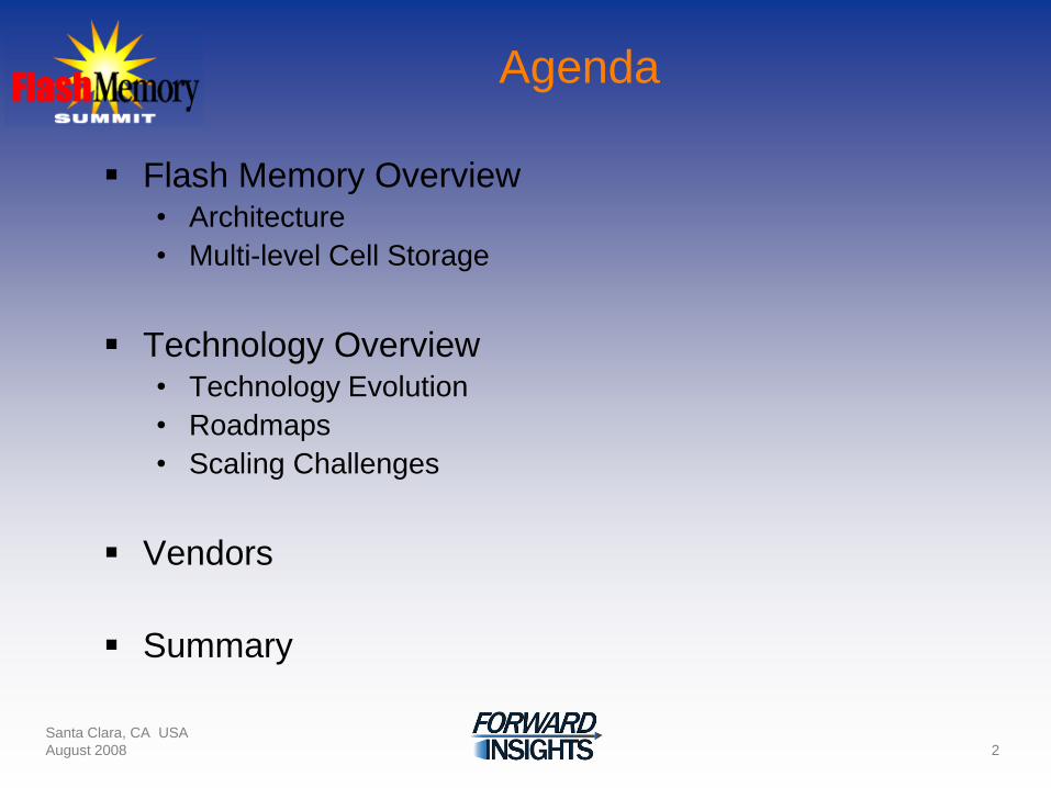
Agenda
Flash Memory Overview• Architecture
• Multi-level Cell Storage
Technology Overview• Technology Evolution
• Roadmaps
• Scaling Challenges
Vendors
Summary

Array Architectures
Santa Clara, CA USA
August 2008 3
Bit line
Bit line
Word line
Source line
Bit line
Bit line
Sourceline select
Bitline select
Source
Source
Word line
NOR NAND NROM
Source/Drain
• Parallel architecture
• 10F2
• Serial architecture
• 4F2
• Parallel architecture
• 7F2

NAND vs. NOR
Santa Clara, CA USA
August 2008 4
random access serial access
Access speed:
Random: 10-50µs
serial (page mode): 25-50ns
write speed:
random: 200µs/byte
page: 200µs/page (0,4µs/byte)
Access time:
Random: 60-120ns
page mode/burst mode:
30ns/15ns
write speed:
random: 10µs/byte or word
• Low Cost
• small cell size
• High sustained write
• page write
• High Performance optimized
• fast random read
• fast random write
Flash Memory
NANDNOR

NROM vs. Floating Gate
Santa Clara, CA USA
August 2008 5
NROM Floating Gate
Bit 2Bit 1
Floating
Gate (Poly) Gate Oxide
Poly
Oxide
• localized storage in nitride traps
• 2 physical bits per cell
• multi-level cell storage allows storage
of 2 electrical bits per cell
• physical storage of charge in floating gate
•multi-level cell storage allows storage of 2
or more electrical bits per cell
Bit 1
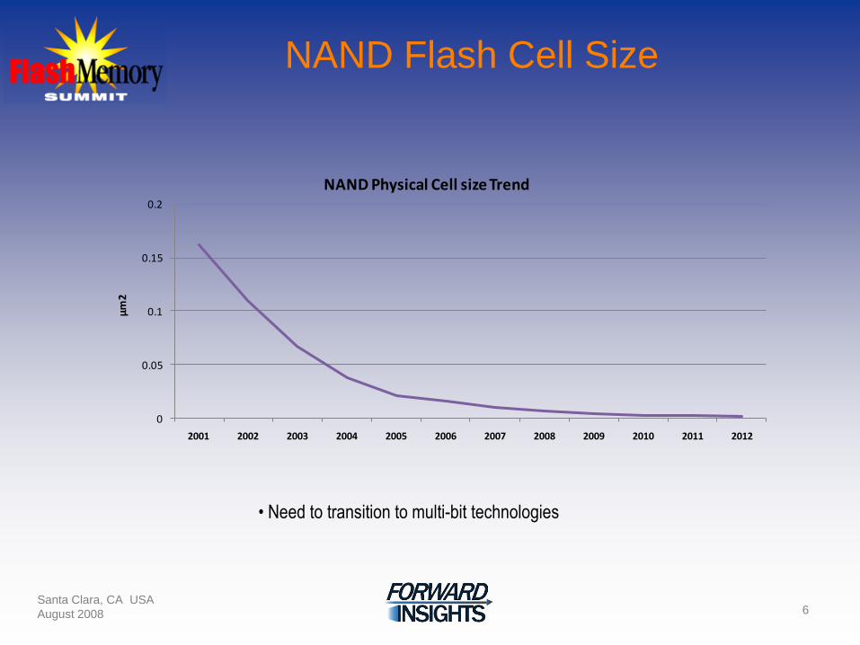
NAND Flash Cell Size
6
• Need to transition to multi-bit technologies
Santa Clara, CA USA
August 2008
0
0.05
0.1
0.15
0.2
2001 2002 2003 2004 2005 2006 2007 2008 2009 2010 2011 2012
µm
2
NAND Physical Cell size Trend

Multi-level Cell Storage - NAND
Santa Clara, CA USA
August 2008 7
S D
Substrate
FG
CG
1010 1000100111101111 11001101 00100011 0000000101100111 010001011011
# o
f ce
lls
110111 100101# o
f ce
lls
01# o
f ce
lls
4 bits/cell
010011 000001110111 100101# o
f ce
lls
3 bits/cell
2 bits/cell
1 bit/cell
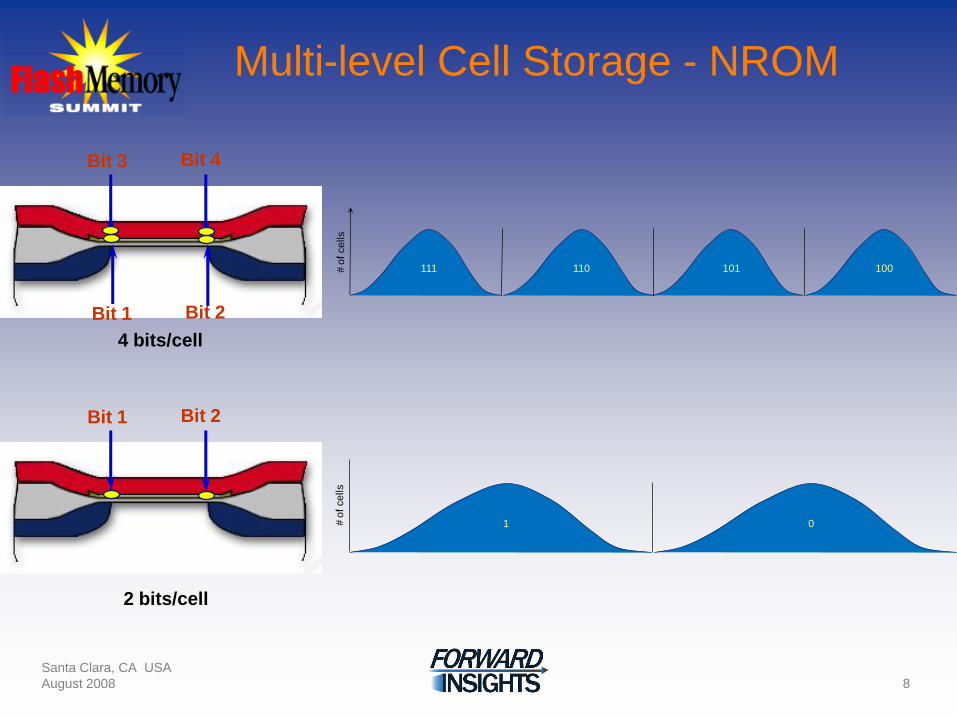
Multi-level Cell Storage - NROM
Santa Clara, CA USA
August 2008 8
Bit 2Bit 1
Bit 4Bit 3
Bit 2Bit 1
110111 100101# o
f ce
lls
01# o
f ce
lls
2 bits/cell
4 bits/cell

9
4Gb SLC NAND
70nm
156mm2
4Gb SLC NAND
70nm
145mm2
8Gb MLC NAND
70nm
146mm2
Samsung Hynix Toshiba
8Gb Quad NROM
75nm
120mm2
Saifun
Images: Semiconductor Insights, Inc., Saifun Semiconductors, Toshiba
16Gb 4b/c NAND
70nm
168mm2
Toshiba
Multi-level Cell Storage Cost
Advantage
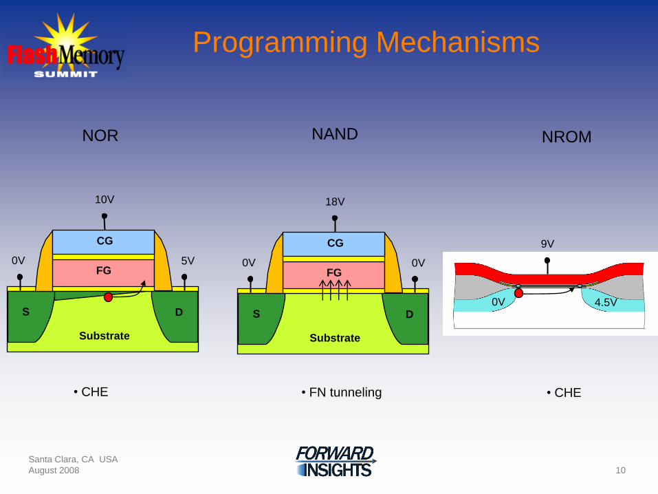
Programming Mechanisms
Santa Clara, CA USA
August 2008 10
S D
Substrate
FG
CG
10V
0V 5V
S D
Substrate
FG
CG
18V
0V 0V
NOR NAND NROM
• CHE • FN tunneling • CHE
9V
4.5V0V

Erase Mechanisms
Santa Clara, CA USA
August 2008 11
S D
Substrate
FG
CG
-18V
0V 5V
S D
Substrate
FG
CG
0V 0V
NOR NAND NROM
• FN tunneling • FN tunneling • BBHHI
-7V
5V0V
18V

Read Mechanisms
Santa Clara, CA USA
August 2008 12
S D
Substrate
FG
CG
3V
0V 1V
NOR NAND NROM
3V
2V0V
4.5V
0V
4.5V
Selected WL
Unselected WL
0.8V0.8V0.8VBL=0.8V
0V
4.5V
4.5V
Unselected WL

Images: Intel Corp.
13
2002 - 130nm
2004 - 90nm
2000 - 180nm
2006 - 65nm
2008 - 45nm
NOR Flash Technology Evolution
Santa Clara, CA USA
August 2008

14
2006 - 60nm
2007 - 50nm
2004 - 90nm
2008 - 40nm
Images: Samsung, Semiconductor Insights, Toshiba
NAND Flash Technology Evolution
Santa Clara, CA USA
August 2008
15
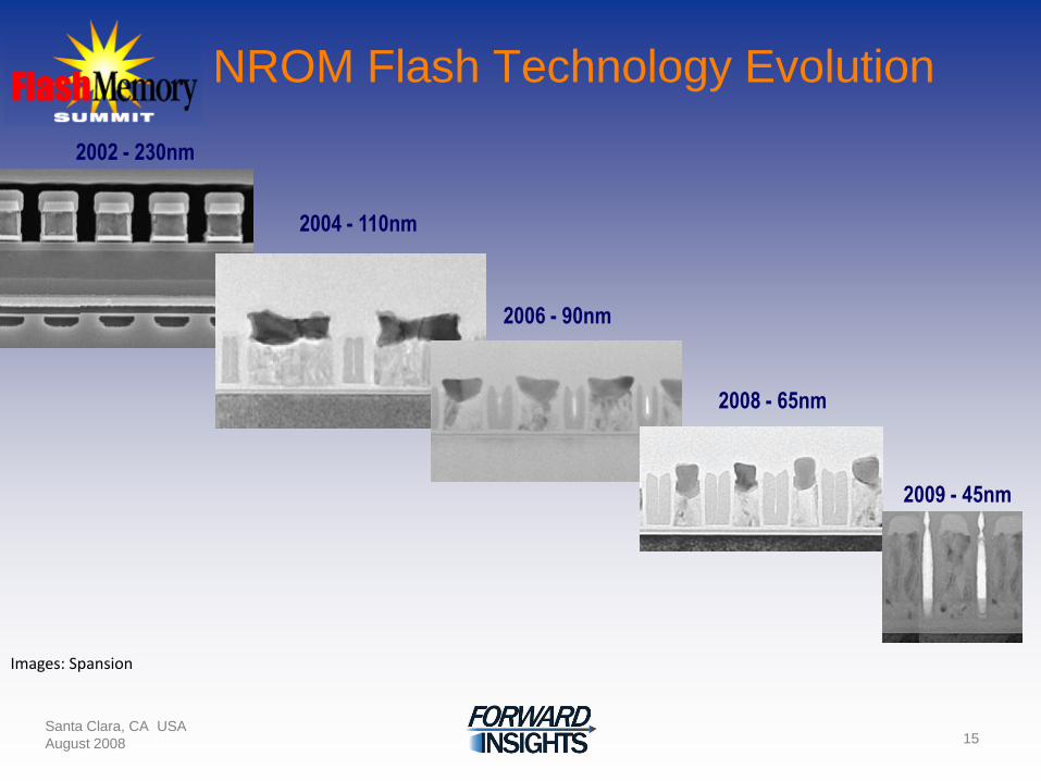
2004 - 110nm
2006 - 90nm
2002 - 230nm
Images: Spansion
2008 - 65nm
2009 - 45nm
NROM Flash Technology Evolution
Santa Clara, CA USA
August 2008

Code Flash Roadmap
16Santa Clara, CA USA
August 2008
128
256
512
1024
2048
4096
64
128
256
512
1024
10
100
1000
10000
2000 2001 2002 2003 2004 2005 2006 2007 2008 2009 2010 2011 2012
De
nsi
ty (
Mb
)
Code Flash Density Trend
MLC NOR NROM Code Source: Forward Insights
• NROM code to be superseded by Eclipse

Data Flash Roadmap
Santa Clara, CA USA
August 2008 17
1024
2048
4096
8192
16384
32768
65536
2048
8192
16384
100
1000
10000
100000
2000 2001 2002 2003 2004 2005 2006 2007 2008 2009 2010 2011 2012
De
nsi
ty (
Mb
)Data Flash Density Trend
MLC NAND NROM QUAD Source: Forward Insights
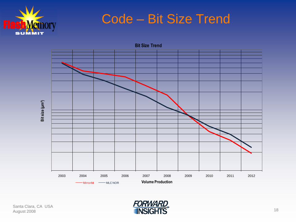
Code – Bit Size Trend
18Santa Clara, CA USA
August 2008
2003 2004 2005 2006 2007 2008 2009 2010 2011 2012
Bit
siz
e (µ
m²)
Volume Production
Bit Size Trend
Mirrorbit MLC NOR
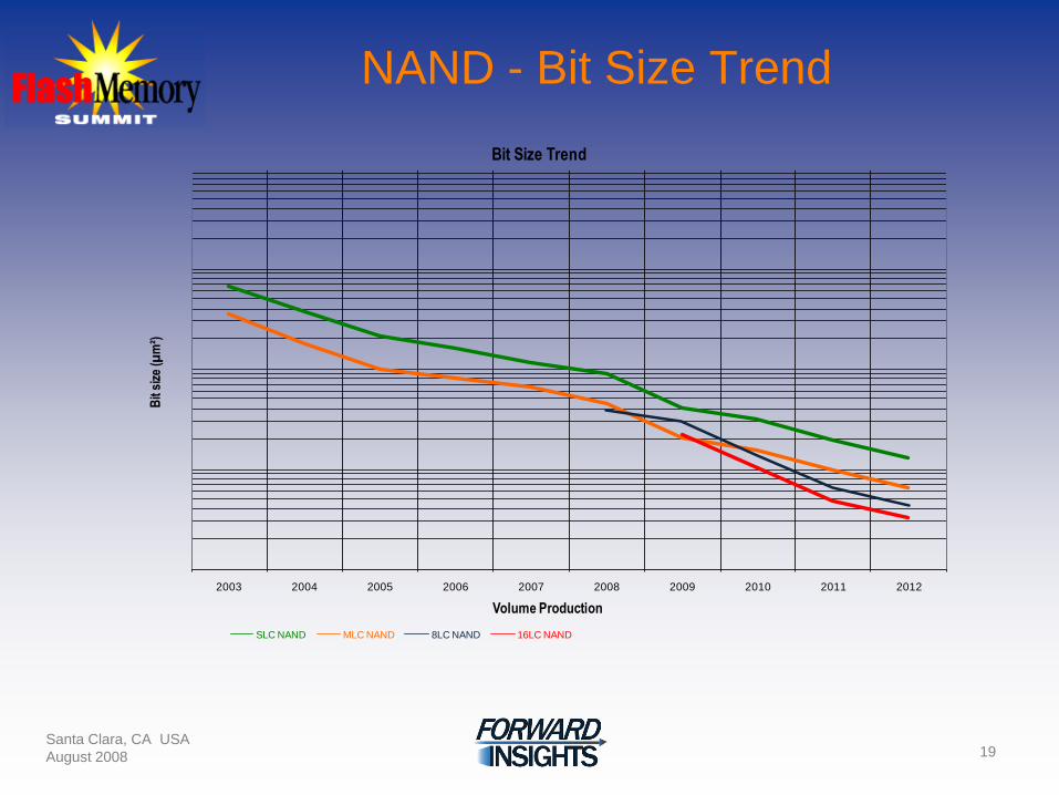
NAND - Bit Size Trend
19Santa Clara, CA USA
August 2008
2003 2004 2005 2006 2007 2008 2009 2010 2011 2012
Bit
size
(µm
²)
Volume Production
Bit Size Trend
SLC NAND MLC NAND 8LC NAND 16LC NAND

20Santa Clara, CA USA
August 2008
Scaling Challenges
NOR Flash NAND Flash NROM
•Short channel
effect
•Contact and
isolation fill
•Charge storage
reduction
•Inter-cell
interference
•CG-FG coupling
•Gap fill
•Charge storage
reduction
•Short channel
effect
•Bit disturbs

NOR Flash Vendors
• Numonyx
– $2.4 billion merger of ST’s (48.6%) and Intel’s (45.1%) NOR businesses; Francisco Partners
owns 6.3%
– Includes ST’s Catania and AMK8 fabs, stake in ST-Hynix Wuxi fab and Intel’s fab 18
– Intel contributed Pudong & Kiveta assembly & test facilities
– Transitioning to 45nm
• Samsung
– Focus on high density NOR for MCPs
– NOR manufactured on legacy 200mm fabs
– 65nm in volume
• Toshiba
– NOR flash for MCPs
– 1st MLC products on 70nm ramping
21Santa Clara, CA USA
August 2008

NOR Flash Vendors
• Macronix
– Focus on serial flash and low density parallel NOR flash on 110nm
• Winbond
– Focus on serial flash
– 90nm NOR flash in 300mm fab ramping in 2H/08
22Santa Clara, CA USA
August 2008

• Samsung
– Fungible production capacity between NAND and DRAM
– Volume production of 42nm
• Toshiba/SanDisk
– NAND manufacturing JV: FlashPartners, FlashAlliance
– Fundamental NAND and MLC patents
– Volume production of 43nm
– First to market with x3, x4 technology: 16Gb x3 in production
• Hynix/Numonyx
– NAND joint development and manufacturing JV
– Volume production of 48nm
23Santa Clara, CA USA
August 2008
NAND Flash Vendors

• Intel/Micron
– NAND joint development and manufacturing JV
– Sampling 34nm 32Gb MLC device
• Powerchip
– 70nm in volume
– 50nm in development
24Santa Clara, CA USA
August 2008
NAND Flash Vendors
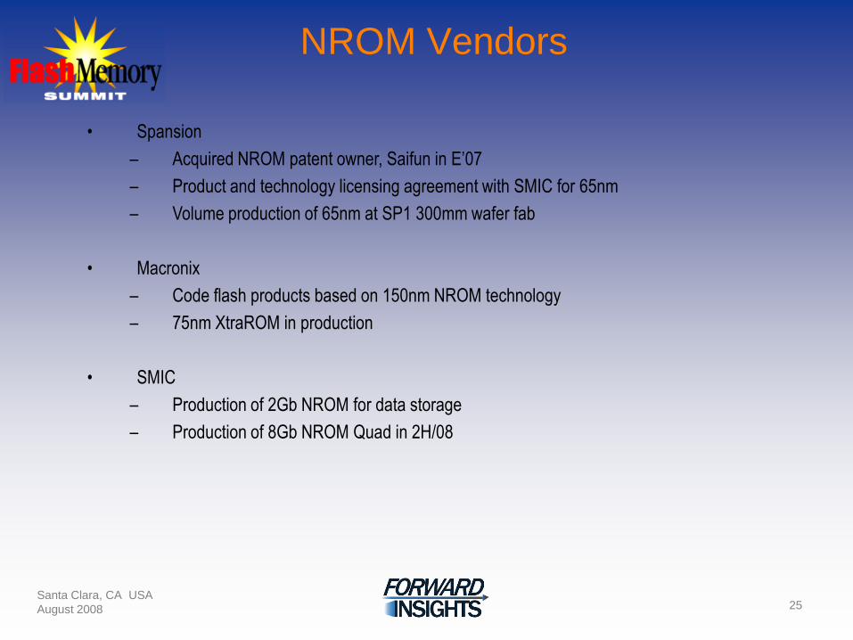
• Spansion
– Acquired NROM patent owner, Saifun in E’07
– Product and technology licensing agreement with SMIC for 65nm
– Volume production of 65nm at SP1 300mm wafer fab
• Macronix
– Code flash products based on 150nm NROM technology
– 75nm XtraROM in production
• SMIC
– Production of 2Gb NROM for data storage
– Production of 8Gb NROM Quad in 2H/08
25Santa Clara, CA USA
August 2008
NROM Vendors

26Santa Clara, CA USA
August 2008
Summary
NOR and NROM most suitable for code storage; NAND for data storage
Move to multi-bit storage to drive further cost reductions as technology scaling slows
Cost benefits of 3bit/cell & 4bit/cell to materialize in next two years

27Santa Clara, CA USA
August 2008
Acknowledgements
Special thanks for the use of material/images
IEEE
Intel
Semiconductor Insights
Spansion

28Santa Clara, CA USA
August 2008
Forward Thinking
www.forward-insights.com