flexible and tunable silicon photonic circuits on plastic ... · flexible and tunable silicon...
TRANSCRIPT
Flexible and tunable silicon photoniccircuits on plastic substratesYu Chen, Huan Li & Mo Li
Department of Electrical and Computer Engineering, University of Minnesota, Minneapolis, MN 55455, USA.
Flexible microelectronics has shown tremendous promise in a broad spectrum of applications, especiallythose that cannot be addressed by conventional microelectronics in rigid materials and constructions. Theseunconventional yet important applications range from flexible consumer electronics to conformal sensorarrays and biomedical devices. A recent paradigm shift in implementing flexible electronics is to physicallytransfer highly integrated devices made in high-quality, crystalline semiconductors on to plastic substrates.Here we demonstrate a flexible form of silicon photonics using the transfer-and-bond fabrication method.Photonic circuits including interferometers and resonators have been transferred onto flexible plasticsubstrates with preserved functionalities and performance. By mechanically deforming, the opticalcharacteristics of the devices can be tuned reversibly over a remarkably large range. The demonstration ofthe new flexible photonic systems based on the silicon-on-plastic (SOP) platform could open the door tomany future applications, including tunable photonics, optomechanical sensors and biomechanical andbio-photonic probes.
The transfer-and-bond methods have been successfully implemented to fabricate flexible microelectronics1–5.Instead of direct deposition of amorphous and low-quality or organic semiconducting materials6–8, theintegration on plastic substrates is achieved by physically transferring integrated devices from wafer sub-
strates. The methods have been improved further with innovative mechanical designs to achieve stretchable andeven foldable devices2,5, spawning many unprecedented applications, most notably, in bio-inspired and implan-table biomedical devices9. The new hybrid form of flexible microelectronics combines the best properties of twomaterial worlds: the high electrical performance of crystalline inorganic semiconductor materials with themechanical flexibility and the bio-compatibility of organic ones. Sophisticated analog and digital CMOS circuitscan be transferred from silicon wafer substrates to a variety of polymeric films and retain their electricalperformance and functionality in the flexible form and under mechanical deformation4. Beyond silicon micro-electronics, the hybrid approach of flexible devices has been successfully applied to a wide range of micro-devicesin diverse materials, including III-V electronics10, microwave electronics11,12, carbon electronics13–16, optoelec-tronics17–19, and very recently plasmonics20,21 and meta-materials22.
Silicon photonics will enjoy the success of flexible microelectronics if they can also be transformed into aflexible form23. The transfer-and-bond approach is particularly viable and appealing to silicon photonics becausecrystalline silicon has superior optical properties, including a high refractive index and low optical loss, which arenot attainable with plastic materials. There are several additional considerations that make the prospect of flexibleintegrated photonics uniquely promising. First, the path of light can be bent when it is guided in optical fibers orwaveguides. Although glass fibers typically can only be bent to a radius of 1 cm before incurring significant loss,thanks to silicon’s high refractive index (n53.5), silicon waveguides can make a turn with a radius as small as a fewmicrons without significant loss24,25. Second, unlike electronic devices, optical devices can be coupled with eachother without being in physical contact — light can propagate through transparent material to couple multiplelayers of optical devices. This attribute of contact-free connection could enable three-dimensional integration ofphotonic systems. Third, there are abundant compliant and patternable plastic materials with low refractive indexand low optical absorption that are suitable for optical applications, including elastomer such as polydimethylsi-loxane (PDMS), polyester such as PET (polyethylene terephthalate) and PEN (polyethylene naphthalate), andepoxies such as SU-8. Finally, the concern of silicon devices’ mechanical fragility and structural stability can beaddressed by the same mechanical design strategies developed for flexible electronics26.
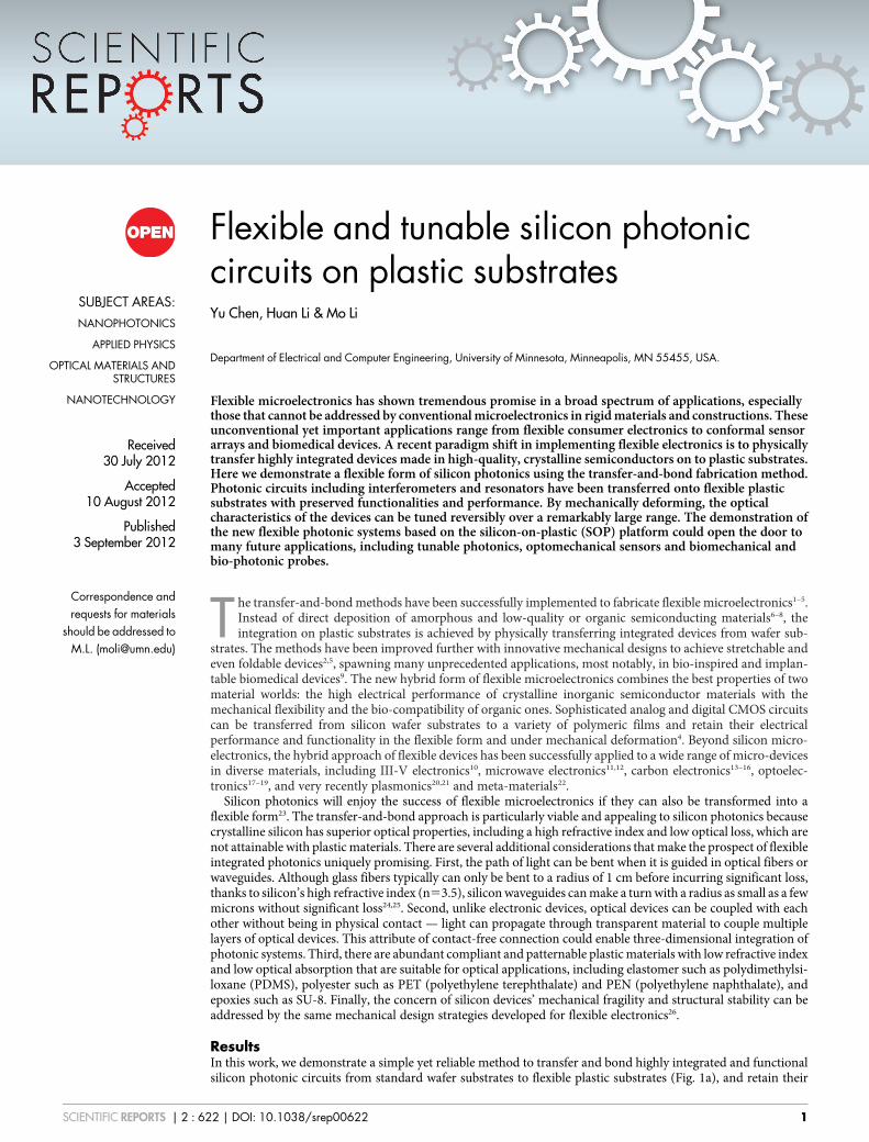
ResultsIn this work, we demonstrate a simple yet reliable method to transfer and bond highly integrated and functionalsilicon photonic circuits from standard wafer substrates to flexible plastic substrates (Fig. 1a), and retain their
SUBJECT AREAS:NANOPHOTONICS
APPLIED PHYSICS
OPTICAL MATERIALS ANDSTRUCTURES
NANOTECHNOLOGY
Received30 July 2012
Accepted10 August 2012
Published3 September 2012
Correspondence andrequests for materials
should be addressed toM.L. ([email protected])
SCIENTIFIC REPORTS | 2 : 622 | DOI: 10.1038/srep00622 1
optical performance as on the original rigid substrates. The fabrica-tion processes are illustrated in Fig. 1b and described in detail in theMethod section. Briefly, silicon photonic circuits are first patternedin the conventional way using electron beam lithography and plasmadry etching. Subsequently, the substrate is chemically etched for aprecise period of time to etch the buried oxide (BOX) layer andcritically undercut the silicon device layer. The undercut reducesthe interfacial area between the silicon and the BOX layers so thatthe total bonding force between them is weakened. It is important tonote that, because they are still affixed to the substrate after theetching, the devices will not move during this step. Next, a PDMSfilm is carefully laminated onto the substrate and peeled off at aconstant speed. When the peeling speed is sufficiently high, thePDMS-silicon adhesion force can be sufficiently strong to overcomethe total bonding force at the silicon-BOX interface27, which has beenreduced to the minimal level by the previous etching step. In this way,the whole silicon photonic layer is lifted off from the substrate andtransferred on to the flexible PDMS film. Because no adhesive mater-ial is used in the procedure, contamination to the photonic devicesand consequent adverse effects on their optical performance is min-imal. The strong bonding force between silicon and PDMS surfaces,however, can ensure high-yield transfer with low occurrence of dis-locations and deformations. Fig. 1c and d shows optical micro-scope images of typical photonic circuits, including Mach-Zehnder
interferometers (MZI) and micro-ring add-drop filters (ADF), afterbeing transferred on to PDMS films. The devices consist of single-mode silicon waveguides (width, 500 nm; thickness, 220 nm) with atotal length as long as 1 centimeter — an aspect ratio of 23104. Asshown in the images, deformations and dislocations are hardlynoticeable in the transferred devices. Most notably, high magnifica-tion images in Fig. 1c and d (lower panels) reveal that the couplinggaps between the waveguides as small as 100 nm wide are preciselypreserved in the fabrication process.
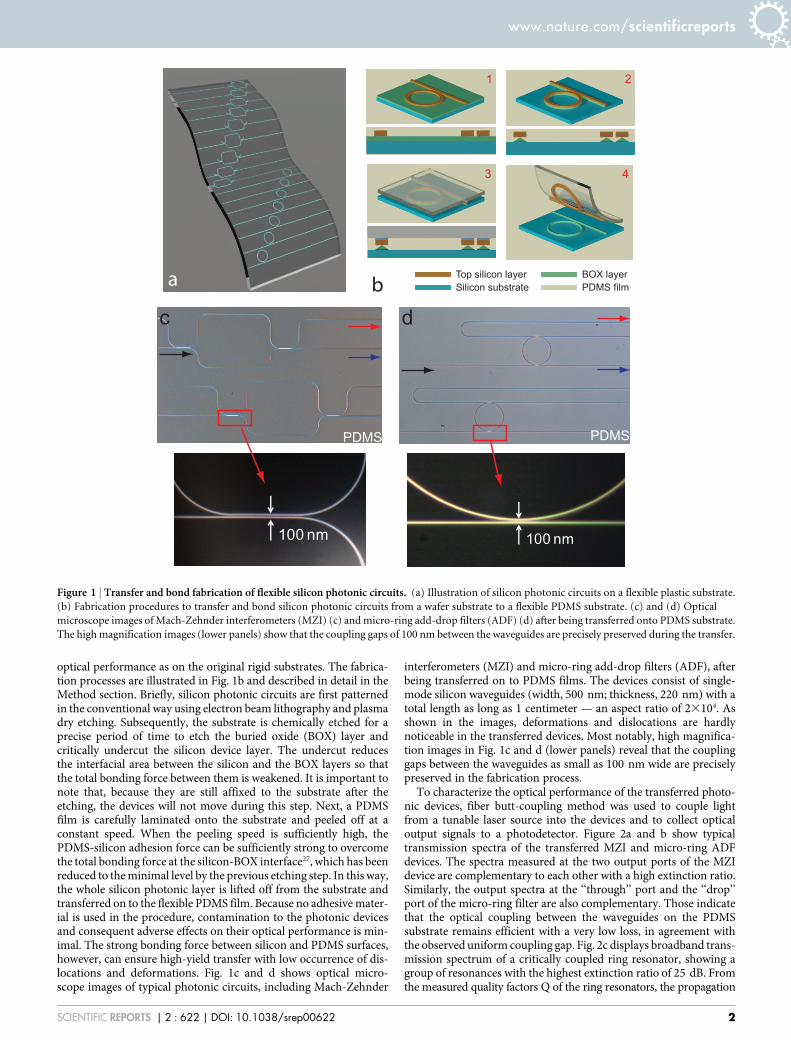
To characterize the optical performance of the transferred photo-nic devices, fiber butt-coupling method was used to couple lightfrom a tunable laser source into the devices and to collect opticaloutput signals to a photodetector. Figure 2a and b show typicaltransmission spectra of the transferred MZI and micro-ring ADFdevices. The spectra measured at the two output ports of the MZIdevice are complementary to each other with a high extinction ratio.Similarly, the output spectra at the ‘‘through’’ port and the ‘‘drop’’port of the micro-ring filter are also complementary. Those indicatethat the optical coupling between the waveguides on the PDMSsubstrate remains efficient with a very low loss, in agreement withthe observed uniform coupling gap. Fig. 2c displays broadband trans-mission spectrum of a critically coupled ring resonator, showing agroup of resonances with the highest extinction ratio of 25 dB. Fromthe measured quality factors Q of the ring resonators, the propagation
ba
100 nm
c
100 nm
PDMS PDMS
d
Top silicon layerSilicon substrate
BOX layerPDMS film
1
3
2
4
Figure 1 | Transfer and bond fabrication of flexible silicon photonic circuits. (a) Illustration of silicon photonic circuits on a flexible plastic substrate.
(b) Fabrication procedures to transfer and bond silicon photonic circuits from a wafer substrate to a flexible PDMS substrate. (c) and (d) Optical
microscope images of Mach-Zehnder interferometers (MZI) (c) and micro-ring add-drop filters (ADF) (d) after being transferred onto PDMS substrate.
The high magnification images (lower panels) show that the coupling gaps of 100 nm between the waveguides are precisely preserved during the transfer.
www.nature.com/scientificreports
SCIENTIFIC REPORTS | 2 : 622 | DOI: 10.1038/srep00622 2
loss in the transferred waveguide can be determined. Fig. 3d shows anunder-coupled resonance at 1593.55 nm with a waveguide loaded Qof 9.93104. It corresponds to an intrinsic Q of 1.53105 and a pro-pagation loss of 3.8 dB/cm. This value of propagation loss is compar-able to that of the original silicon waveguides on a SOI substrate,which typically is in the range of 3–4 dB/cm if no special fabricationoptimization is used24. It is unlikely that optical absorption in thePDMS substrate causes an increase of loss because of its transparencein the near-infrared spectral range28,29. We attribute any excessive lossto oxide residue and other contaminations on the waveguide surface,which can be etched away or reduced with improved transfer process.The above results demonstrate that the transfer method developedhere preserves the optical performance and functionalities of the sil-icon photonic devices on the new plastic substrate.
Tunable photonic devices are highly desirable for applicationsin optical network systems that can be frequently reconfigured30.Conventional tuning methods either use the electro-optical effectsin non-silicon materials such as lithium niobate (LiNbO3)31,32, whichis difficult to integrate with silicon devices, or rely on the thermo-optical effect by electrically heating the devices33,34. The heatingmethod, although integratable, needs to continuously consume elec-trical power to maintain the tuning. Because optical characteristics ofthe flexible devices apparently will change when the substrate isdeformed, their functionalities can be precisely tuned by applying acontrolled force, using a piezoelectric actuator for instance. Below theyield limit of the substrate material which is significantly higher forplastic materials (,50% for PDMS) than for crystalline materials(less than 1% for crystalline silicon), the device structure will respondelastically to the applied force, and reversible and reliable tuning canbe achieved over a large range.
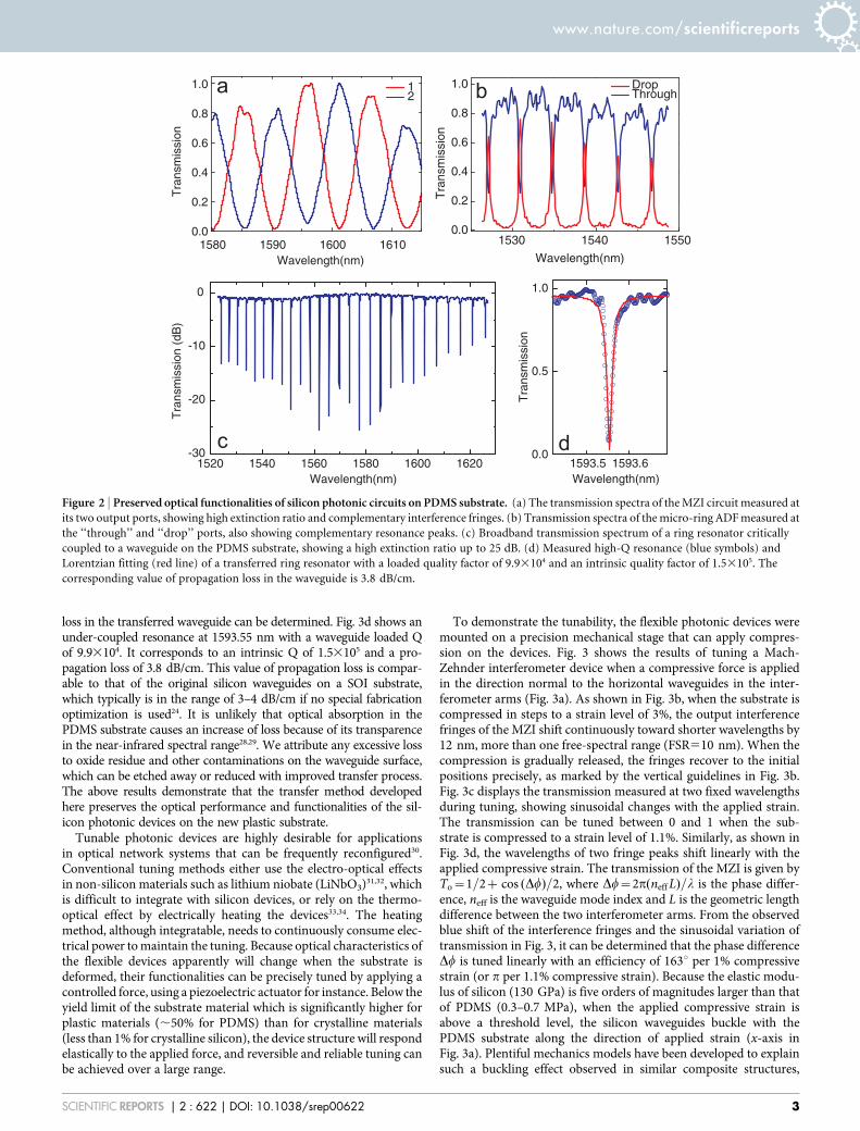
To demonstrate the tunability, the flexible photonic devices weremounted on a precision mechanical stage that can apply compres-sion on the devices. Fig. 3 shows the results of tuning a Mach-Zehnder interferometer device when a compressive force is appliedin the direction normal to the horizontal waveguides in the inter-ferometer arms (Fig. 3a). As shown in Fig. 3b, when the substrate iscompressed in steps to a strain level of 3%, the output interferencefringes of the MZI shift continuously toward shorter wavelengths by12 nm, more than one free-spectral range (FSR510 nm). When thecompression is gradually released, the fringes recover to the initialpositions precisely, as marked by the vertical guidelines in Fig. 3b.Fig. 3c displays the transmission measured at two fixed wavelengthsduring tuning, showing sinusoidal changes with the applied strain.The transmission can be tuned between 0 and 1 when the sub-strate is compressed to a strain level of 1.1%. Similarly, as shown inFig. 3d, the wavelengths of two fringe peaks shift linearly with theapplied compressive strain. The transmission of the MZI is given byTo~1=2z cos (Dw)=2, where Dw~2p(neff L)=l is the phase differ-ence, neff is the waveguide mode index and L is the geometric lengthdifference between the two interferometer arms. From the observedblue shift of the interference fringes and the sinusoidal variation oftransmission in Fig. 3, it can be determined that the phase differenceDw is tuned linearly with an efficiency of 163u per 1% compressivestrain (or p per 1.1% compressive strain). Because the elastic modu-lus of silicon (130 GPa) is five orders of magnitudes larger than thatof PDMS (0.3–0.7 MPa), when the applied compressive strain isabove a threshold level, the silicon waveguides buckle with thePDMS substrate along the direction of applied strain (x-axis inFig. 3a). Plentiful mechanics models have been developed to explainsuch a buckling effect observed in similar composite structures,
1580 1590 1600 16100.0
0.2
0.4
0.6
0.8
1.0
Tra
nsm
issi
on
Wavelength(nm)
1530 1540 15500.0
0.2
0.4
0.6
0.8
1.0 Drop Through
Tra
nsm
issi
on
Wavelength(nm)
1520 1540 1560 1580 1600 1620-30
-20
-10
0
Tra
nsm
issi
on (
dB)
Wavelength(nm)
ba 1 2
c1593.5 1593.6
0.0
0.5
1.0
Tra
nsm
issi
on
Wavelength(nm)
d
Figure 2 | Preserved optical functionalities of silicon photonic circuits on PDMS substrate. (a) The transmission spectra of the MZI circuit measured at
its two output ports, showing high extinction ratio and complementary interference fringes. (b) Transmission spectra of the micro-ring ADF measured at
the ‘‘through’’ and ‘‘drop’’ ports, also showing complementary resonance peaks. (c) Broadband transmission spectrum of a ring resonator critically
coupled to a waveguide on the PDMS substrate, showing a high extinction ratio up to 25 dB. (d) Measured high-Q resonance (blue symbols) and
Lorentzian fitting (red line) of a transferred ring resonator with a loaded quality factor of 9.93104 and an intrinsic quality factor of 1.53105. The
corresponding value of propagation loss in the waveguide is 3.8 dB/cm.
www.nature.com/scientificreports
SCIENTIFIC REPORTS | 2 : 622 | DOI: 10.1038/srep00622 3
mostly in the context of flexible microelectronics, and can be appliedhere35–37. The buckling amplitude A is given by A~h
ffiffiffiffiffiffiffiffiffiffiffiffiffiffiffiffiffiffiffiffiffiffi{ea=ec{1
p=
(1z0:84ea), where h50.22 mm is the thickness of the silicon layerand ea is applied strain (negative for compressive strain). ec~(3�Es=�Ef )
2=3=4 is the critical strain above which buckling happens.In the silicon/PDMS composite, the plain-strain modulus are�Ef ~140 GPa for silicon and �Es~2:3 MPa for PDMS, thus ec equals0.03% which is smaller than the minimal strain (,0.1%) that can bereliably applied in our experiment. Therefore, during the tuning, thewaveguides along the direction of applied strain always buckle. Thebuckling amplitude A at the maximal compressive strain (23%)applied in the tuning experiment is calculated to be 2.1 mm. Sincethe geometric length of the waveguide increases when it buckles, theobserved decrease in the phase difference Dw can only be attributedto the reduction of the waveguide mode index neff from the photo-elastic effect of silicon38. Detailed analysis in the supplementaryinformation reveals that neff of the fundamental TE mode of thewaveguide along the direction of strain decreases by Dneff ~g:n3
{r12z(r11zr12)u½ �exx=2, where n, r11 and r12, u are silicon’srefractive index, elasto-optic coefficients and Poisson ratio, respect-ively. g51.15 is the proportional coefficient that relates the change ofthe waveguide mode index and the change of the material refractiveindex and can be determined by simulation. exx is the average normalstrain in the buckled waveguide, which is tensile (positive) and canbe expressed analytically in an approximate form (supplementaryinformation) or determined numerically by simulation. The resultsof the theoretical model are plotted in Fig. 3c and d, showing goodagreement with the experimental results with small discrepancywhich can be attributed to the imprecision of the manual tuningsetup used in the experiment.
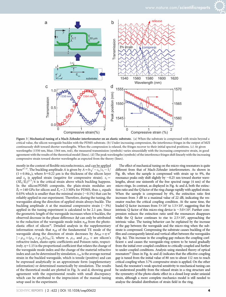
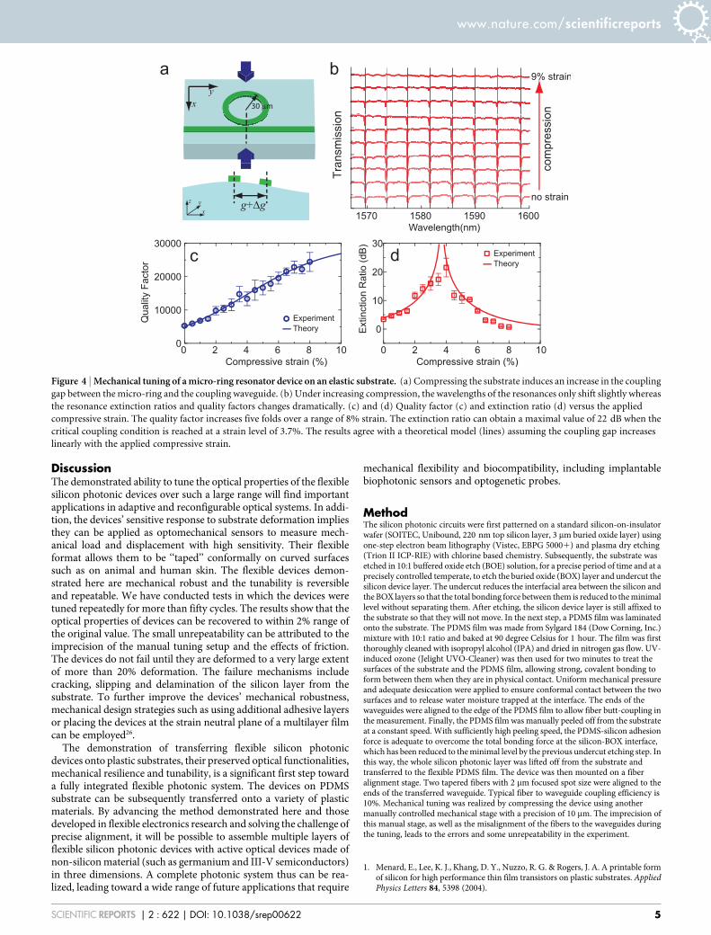
The effect of mechanical tuning on the micro-ring resonators is quitedifferent from that of Mach-Zehnder interferometers. As shown inFig. 4b, when the sample is compressed with strain up to 9%, theresonance peaks only shift slightly by ,0.25 nm toward shorter wave-lengths, about one sixteenth of the free spectral range (4 nm) of themicro-rings. In contrast, as displayed in Fig. 4c and d, both the extinc-tion ratio and the Q factor of the ring change rapidly with applied strain.When the sample is compressed by 4%, the extinction ratio firstincreases from 3 dB to a maximal value of 22 dB, indicating the res-onator reaches the critical coupling condition. At the same time, theloaded Q factor increases from 53103 to 1.53104, suggesting that theintrinsic Q factor of this micro-ring device is ,3.03104. Further com-pression reduces the extinction ratio until the resonances disappearswhile the Q factor continues to rise to 2.53104, approaching theintrinsic value. The tuning behavior can be explained by the increaseof the gap between the waveguide and the micro-ring when the sub-strate is compressed. Compressing the substrate causes buckling of thefilm and consequently lateral and vertical offset between the waveguides(Fig. 4a). This increase in the coupling gap reduces the coupling coef-ficient k and causes the waveguide-ring system to be tuned graduallyfrom the initial over-coupled condition to critically-coupled and furtherto under-coupled conditions. Analysis using standard theory of opticalresonators39 (lines in Fig. 4c and d) indicates that the effective couplinggap is tuned from the initial value of 80 nm to about 112 nm to reachcritical coupling when 3.7% compressive strain is applied. On the otherhand, the resonator’s weak spectral sensitivity to mechanical tuning canbe understood possibly from the relaxed strain in a ring structure andthe symmetry of the photo-elastic effect in a closed loop under uniaxialstrain, although a more complete mechanics model is still needed toanalyze the detailed distribution of strain field in the ring.
Figure 3 | Mechanical tuning of a Mach-Zehnder interferometer on an elastic substrate. (a) When the substrate is compressed with strain beyond a
critical value, the silicon waveguide buckles with the PDMS substrate. (b) Under increasing compression, the interference fringes in the output of MZI
continuously shift toward shorter wavelengths. When the compression is relaxed, the fringes recover to their initial spectral positions. (c) At given
wavelengths (1550 nm, blue; 1564 nm, red), the measured transmission (symbols) varies sinusoidally with the increasing compressive strain, in good
agreement with the results of the theoretical model (lines). (d) The peak wavelengths (symbols) of the interference fringes shift linearly with the increasing
compressive strain toward shorter wavelengths as expected from the theory (lines).
www.nature.com/scientificreports
SCIENTIFIC REPORTS | 2 : 622 | DOI: 10.1038/srep00622 4
DiscussionThe demonstrated ability to tune the optical properties of the flexiblesilicon photonic devices over such a large range will find importantapplications in adaptive and reconfigurable optical systems. In addi-tion, the devices’ sensitive response to substrate deformation impliesthey can be applied as optomechanical sensors to measure mech-anical load and displacement with high sensitivity. Their flexibleformat allows them to be ‘‘taped’’ conformally on curved surfacessuch as on animal and human skin. The flexible devices demon-strated here are mechanical robust and the tunability is reversibleand repeatable. We have conducted tests in which the devices weretuned repeatedly for more than fifty cycles. The results show that theoptical properties of devices can be recovered to within 2% range ofthe original value. The small unrepeatability can be attributed to theimprecision of the manual tuning setup and the effects of friction.The devices do not fail until they are deformed to a very large extentof more than 20% deformation. The failure mechanisms includecracking, slipping and delamination of the silicon layer from thesubstrate. To further improve the devices’ mechanical robustness,mechanical design strategies such as using additional adhesive layersor placing the devices at the strain neutral plane of a multilayer filmcan be employed26.
The demonstration of transferring flexible silicon photonicdevices onto plastic substrates, their preserved optical functionalities,mechanical resilience and tunability, is a significant first step towarda fully integrated flexible photonic system. The devices on PDMSsubstrate can be subsequently transferred onto a variety of plasticmaterials. By advancing the method demonstrated here and thosedeveloped in flexible electronics research and solving the challenge ofprecise alignment, it will be possible to assemble multiple layers offlexible silicon photonic devices with active optical devices made ofnon-silicon material (such as germanium and III-V semiconductors)in three dimensions. A complete photonic system thus can be rea-lized, leading toward a wide range of future applications that require
mechanical flexibility and biocompatibility, including implantablebiophotonic sensors and optogenetic probes.
MethodThe silicon photonic circuits were first patterned on a standard silicon-on-insulatorwafer (SOITEC, Unibound, 220 nm top silicon layer, 3 mm buried oxide layer) usingone-step electron beam lithography (Vistec, EBPG 50001) and plasma dry etching(Trion II ICP-RIE) with chlorine based chemistry. Subsequently, the substrate wasetched in 10:1 buffered oxide etch (BOE) solution, for a precise period of time and at aprecisely controlled temperate, to etch the buried oxide (BOX) layer and undercut thesilicon device layer. The undercut reduces the interfacial area between the silicon andthe BOX layers so that the total bonding force between them is reduced to the minimallevel without separating them. After etching, the silicon device layer is still affixed tothe substrate so that they will not move. In the next step, a PDMS film was laminatedonto the substrate. The PDMS film was made from Sylgard 184 (Dow Corning, Inc.)mixture with 10:1 ratio and baked at 90 degree Celsius for 1 hour. The film was firstthoroughly cleaned with isopropyl alcohol (IPA) and dried in nitrogen gas flow. UV-induced ozone (Jelight UVO-Cleaner) was then used for two minutes to treat thesurfaces of the substrate and the PDMS film, allowing strong, covalent bonding toform between them when they are in physical contact. Uniform mechanical pressureand adequate desiccation were applied to ensure conformal contact between the twosurfaces and to release water moisture trapped at the interface. The ends of thewaveguides were aligned to the edge of the PDMS film to allow fiber butt-coupling inthe measurement. Finally, the PDMS film was manually peeled off from the substrateat a constant speed. With sufficiently high peeling speed, the PDMS-silicon adhesionforce is adequate to overcome the total bonding force at the silicon-BOX interface,which has been reduced to the minimal level by the previous undercut etching step. Inthis way, the whole silicon photonic layer was lifted off from the substrate andtransferred to the flexible PDMS film. The device was then mounted on a fiberalignment stage. Two tapered fibers with 2 mm focused spot size were aligned to theends of the transferred waveguide. Typical fiber to waveguide coupling efficiency is10%. Mechanical tuning was realized by compressing the device using anothermanually controlled mechanical stage with a precision of 10 mm. The imprecision ofthis manual stage, as well as the misalignment of the fibers to the waveguides duringthe tuning, leads to the errors and some unrepeatability in the experiment.
1. Menard, E., Lee, K. J., Khang, D. Y., Nuzzo, R. G. & Rogers, J. A. A printable formof silicon for high performance thin film transistors on plastic substrates. AppliedPhysics Letters 84, 5398 (2004).
Figure 4 | Mechanical tuning of a micro-ring resonator device on an elastic substrate. (a) Compressing the substrate induces an increase in the coupling
gap between the micro-ring and the coupling waveguide. (b) Under increasing compression, the wavelengths of the resonances only shift slightly whereas
the resonance extinction ratios and quality factors changes dramatically. (c) and (d) Quality factor (c) and extinction ratio (d) versus the applied
compressive strain. The quality factor increases five folds over a range of 8% strain. The extinction ratio can obtain a maximal value of 22 dB when the
critical coupling condition is reached at a strain level of 3.7%. The results agree with a theoretical model (lines) assuming the coupling gap increases
linearly with the applied compressive strain.
www.nature.com/scientificreports
SCIENTIFIC REPORTS | 2 : 622 | DOI: 10.1038/srep00622 5
2. Rogers, J. A., Someya, T. & Huang, Y. Materials and Mechanics for StretchableElectronics. Science 327, 1603–1607 (2010).
3. Sun, Y. G. & Rogers, J. A. Inorganic semiconductors for flexible electronics. AdvMater 19, 1897–1916 (2007).
4. Kim, D. H. et al. Stretchable and foldable silicon integrated circuits. Science 320,507–511 (2008).
5. Kim, D.-H. & Rogers, J. A. Stretchable Electronics: Materials Strategies andDevices. Adv Mater 20, 4887–4892 (2008).
6. Garnier, F., Hajlaoui, R., Yassar, A. & Srivastava, P. All-polymer filed-effecttransistor realized by printing techniques. Science 265, 1684–1686 (1994).
7. Forrest, S. R. The path to ubiquitous and low-cost organic electronic appliances onplastic. Nature 428, 911–918 (2004).
8. Salleo, A. & Wong, W. S. Flexible Electronics Materials and Applications.(Springer-Verlag US, 2009).
9. Ko, H. C. et al. A hemispherical electronic eye camera based on compressiblesilicon optoelectronics. Nature 454, 748–753 (2008).
10. Ko, H. et al. Ultrathin compound semiconductor on insulator layers for high-performance nanoscale transistors. Nature 468, 286–289 (2010).
11. Yuan, H. C. & Ma, Z. Q. Microwave thin-film transistors using Si nanomembraneson flexible polymer substrate. Applied Physics Letters 89, – (2006).
12. Sun, L. et al. Flexible high-frequency microwave inductors and capacitorsintegrated on a polyethylene terephthalate substrate. Applied Physics Letters 96, –(2010).
13. Bradley, K., Gabriel, J.-C. P. & Gruner, G. Flexible Nanotube Electronics. NanoLetters 3, 1353–1355 (2003).
14. Eda, G., Fanchini, G. & Chhowalla, M. Large-area ultrathin films of reducedgraphene oxide as a transparent and flexible electronic material. NatureNanotechnology 3, 270–274 (2008).
15. Kim, K. S. et al. Large-scale pattern growth of graphene films for stretchabletransparent electrodes. Nature 457, 706–710 (2009).
16. Sun, D.-m. et al. Flexible high-performance carbon nanotube integrated circuits.Nature Nanotechnology 6, 156–161 (2011).
17. Yuan, H. C. et al. Flexible photodetectors on plastic substrates by use of printingtransferred single-crystal germanium membranes. Applied Physics Letters 94, –(2009).
18. Yoon, J. et al. Flexible concentrator photovoltaics based on microscale silicon solarcells embedded in luminescent waveguides. Nat Commun 2, 343 (2011).
19. Kim, T. I., Kim, R. H. & Rogers, J. A. Microscale Inorganic Light-Emitting Diodeson Flexible and Stretchable Substrates. Ieee Photonics J 4, 607–612 (2012).
20. Pryce, I. M., Aydin, K., Kelaita, Y. A., Briggs, R. M. & Atwater, H. A. HighlyStrained Compliant Optical Metamaterials with Large Frequency Tunability.Nano Letters 10, 4222–4227 (2010).
21. Aksu, S. et al. Flexible Plasmonics on Unconventional and Nonplanar Substrates.Adv Mater 23, 4422 (2011).
22. Chanda, D. et al. Large-area flexible 3D optical negative index metamaterialformed by nanotransfer printing. Nature Nanotechnology 6, 402–407 (2011).
23. Reed, G. T. & Wiley online library. (Wiley, Chichester, 2008).24. Vlasov, Y. A. & McNab, S. J. Losses in single-mode silicon-on-insulator strip
waveguides and bends. Optics Express 12, 1622–1631 (2004).25. Xu, Q., Fattal, D. & Beausoleil, R. G. Silicon microring resonators with 1.5-?m
radius. Optics Express 16, 4309–4315 (2008).26. Yoon, J. et al. Ultrathin silicon solar microcells for semitransparent, mechanically
flexible and microconcentrator module designs. Nat Mater 7, 907–915 (2008).27. Meitl, M. A. et al. Transfer printing by kinetic control of adhesion to an
elastomeric stamp. Nature Materials 5, 33–38 (2005).
28. DeGroot, J. V. J. in Inorganic polymers (eds Roger De Jaeger & Mario, Gleria)(Nova Science Publishers, 2007).
29. Chang-Yen, D. A., Eich, R. K. & Gale, B. K. A monolithic PDMS waveguide systemfabricated using soft-lithography techniques. J Lightwave Technol 23, 2088–2093(2005).
30. Glance, B. Tunable add/drop optical filter providing arbitrary channelarrangements. Photonics Technology Letters, IEEE 7, 1303–1305 (1995).
31. Wooten, E. L., Stone, R. L., Miles, E. W. & Bradley, E. M. Rapidly tunablenarrowband wavelength filter using LiNbO3 unbalanced Mach-Zehnderinterferometers. Lightwave Technology, Journal of 14, 2530–2536 (1996).
32. Mohageg, M. et al. Reconfigurable optical filter. Electronics Letters 41, 356–358(2005).
33. Klein, E. J. et al. Reconfigurable optical add-drop multiplexer using microringresonators. Photonics Technology Letters, IEEE 17, 2358–2360 (2005).
34. Sherwood-Droz, N. et al. Optical 4x4 hitless slicon router for optical networks-on-chip (NoC). Opt. Express 16, 15915–15922 (2008).
35. Huang, Z. Y., Hong, W. & Suo, Z. Nonlinear analyses of wrinkles in a film bondedto a compliant substrate. Journal of the Mechanics and Physics of Solids 53,2101–2118 (2005).
36. Jiang, H. Q. et al. Finite deformation mechanics in buckled thin films oncompliant supports. P Natl Acad Sci USA 104, 15607–15612 (2007).
37. Harrison, C., Stafford, C. M., Zhang, W. & Karim, A. Sinusoidal phase gratingcreated by a tunably buckled surface. Applied Physics Letters 85, 4016–4018(2004).
38. Yariv, A. & Yeh, P. Optical waves in crystals : propagation and control of laserradiation. Wiley classics library edn, (John Wiley and Sons, 2003).
39. Yariv, A. Critical coupling and its control in optical waveguide-ring resonatorsystems. Photonics Technology Letters, IEEE 14, 483–485 (2002).
AcknowledgementThis work was supported partially by NSF Award Number ECCS-1232064 and by theMRSEC Program of NSF under Award Number DMR-0819885. Parts of this work werecarried out in the University of Minnesota Nanofabrication Center which receives partialsupport from NSF through NNIN program, and the Characterization Facility which is amember of the NSF-funded Materials Research Facilities Network via the MRSEC program.
Author contributionsYC performed device fabrication and measurement. HL assisted device design. YC and MLanalyzed the results and developed the theoretical models. YC and ML wrote themanuscript. All authors reviewed the manuscript.
Additional informationSupplementary information accompanies this paper at http://www.nature.com/scientificreports
Competing financial interests: The authors declare no competing financial interests.
License: This work is licensed under a Creative CommonsAttribution-NonCommercial-NoDerivative Works 3.0 Unported License. To view a copyof this license, visit http://creativecommons.org/licenses/by-nc-nd/3.0/
How to cite this article: Chen, Y., Li, H. & Li, M. Flexible and tunable silicon photoniccircuits on plastic substrates. Sci. Rep. 2, 622; DOI:10.1038/srep00622 (2012).
www.nature.com/scientificreports
SCIENTIFIC REPORTS | 2 : 622 | DOI: 10.1038/srep00622 6