flexible packaging for a wireless intraocular pressure
TRANSCRIPT

Flexible Packaging for a Wireless Intraocular Pressure Sensor
Çağdaş Varel
A dissertation
submitted in partial fulfillment of the
requirements for the degree of
Doctor of Philosophy
University of Washington
2013
Reading Committee:
Karl F. Böhringer, Chair
Lih-Yuan Lin
Brian Otis
Program Authorized to Offer Degree:
Electrical Engineering

©Copyright 2013
Çağdaş Varel

University of Washington
Abstract
Flexible Packaging for a Wireless Intraocular Pressure Sensor
Çağdaş Varel
Chair of the Supervisory Committee:
Professor Karl F. Böhringer
Electrical Engineering
This dissertation focuses on the prototype of an intraocular pressure (IOP) sensor as a major step
towards building a device that can be permanently implanted during cataract surgery. The
implantation will proceed through an incision of 2-3 mm using an injector, during which the
complete device must be folded into a cross-section of 2 mm × 1 mm. The device uses radio
frequency (RF) for wireless power and data transfer.
First, a novel device design is introduced. Materials are chosen systematically for the device
fabrication. Two fabrication methods, metal-on-elastomer and solder-filled microchannel, are
tested for the antenna fabrication and device integration. Results indicate that an antenna
resistance below 5 Ω can be achieved using the solder-filled microchannel method. A device
fabrication and integration process based on that method is introduced.
A device prototype including an antenna, an RF chip and a pressure sensor is presented. It is
assembled on a printed circuit board (PCB) with several circuit components used for testing and

calibration. The antenna is fabricated and integrated with the circuit using a fabrication method
employing solder-filled microchannels embedded in an elastomer (polydimethylsiloxane, PDMS).
The presented method can be used for biocompatible packaging of microsystems and sensors.
The prototype is tested for antenna functionality through power and data transfer. The monitoring
device is powered at 2.716 GHz from a distance of 1-2 cm. Transferred power is greater than the
threshold power required for chip operation. Exposure to RF power is kept below the maximum
permissible exposure limit. The backscattered signal is observed in each chip mode to confirm the
wireless sensing capability.
Structural flexibility of the PDMS-metal-PDMS stack is studied using a mockup device. The
effect of applied stress on antenna resistance is monitored in order to evaluate its durability during
the implantation process. The flexible antenna can withstand a stress of 33.4 kPa without any
electrical disconnection. It did not show a significant increase in electrical resistance after 50
bending cycles.
The prototype has undergone electrical tests for the effect of PDMS coating on pressure sensor
and wireless sensing performance. An acceptable increase in sensor capacitance and pressure
sensitivity is observed after PDMS coating. Wireless pressure measurement tests showed device
operation with a pressure sensitivity of 16.66 Hz/mm-Hg (0.125 Hz/Pa).
Three topics for future work are proposed for converting the prototype into a complete device.
First, additional tests for evaluating device performance in an eye-like environment are proposed.
They provide a complete characterization of the RF power and data transfer inside the eye.
Second, requirements for the next generation of RF chip are stated. Device size will be shrunk by
the elimination of surface mount technology (SMT) components and PCB. Third, building a
multi-sensor platform based on the prototype is proposed. Salinity and pH sensors can be added

to the prototype.

i
TABLE OF CONTENTS
Page
LIST OF FIGURES ........................................................................................................................ iii
LIST OF TABLES .......................................................................................................................... vi
CHAPTER 1. Introduction ............................................................................................................... 1
CHAPTER 2. Flexible Packaging Method for an Intraocular Pressure Sensor Implanted during a Cataract Surgery ............................................................................................................................... 5
2.1 Introduction .......................................................................................................... 5
2.2 Packaging Material ............................................................................................... 7
2.3 Fabrication Method .............................................................................................. 8
2.3.1 Metal-on-Elastomer ......................................................................................... 9
2.3.2 Solder-Filled Microchannel ........................................................................... 16
2.3.3 Comparison of Fabrication Methods .............................................................. 20
2.4 Integration Scheme ............................................................................................. 20
2.5 Compatibility with PEU Ring ............................................................................ 23
2.6 Conclusion .......................................................................................................... 24
CHAPTER 3. Prototype of the Intraocular Pressure Monitoring Device ....................................... 25
3.1 Introduction ........................................................................................................ 25
3.2 Device Prototype ................................................................................................ 25
3.3 Prototype Fabrication ......................................................................................... 26
3.3.1 Parts and Part Assembly ................................................................................ 26
3.3.2 Antenna Fabrication and Integration .............................................................. 27
3.3.3 Fabrication Results ......................................................................................... 29
3.4 Conclusion .......................................................................................................... 30
CHAPTER 4. Solder-filled Microchannel Antenna Performance .................................................. 31
4.1 Introduction ........................................................................................................ 31
4.2 RF Power Transfer ............................................................................................. 31
4.3 RF Exposure Limit ............................................................................................. 33

4.4 Transmission of Measurement Results .............................................................. 34
4.5 Conclusion .......................................................................................................... 35
CHAPTER 5. Mechanical Properties of the Solder-filled Antenna Structure ................................ 36
5.1 Introduction ........................................................................................................ 36
5.2 Mockup Device .................................................................................................. 36
5.3 Measurement Setup ............................................................................................ 37
5.4 Results ................................................................................................................ 38
5.5 Conclusion .......................................................................................................... 41
CHAPTER 6. Pressure Measurement ............................................................................................. 42
6.1 Introduction ........................................................................................................ 42
6.2 Effect of PDMS Coating on Pressure Sensor ..................................................... 42
6.3 Wireless Pressure Measurement ......................................................................... 44
6.4 Conclusion .......................................................................................................... 47
CHAPTER 7. Conclusions and Future Work ................................................................................. 48
7.1 Conclusions ........................................................................................................ 48
7.2 Future Work ....................................................................................................... 49
7.2.1 Testing in an Eye Model ................................................................................ 49
7.2.2 From Prototype to a Complete Device ........................................................... 49
7.2.3 Salinity and pH Monitoring ........................................................................... 49
References ……………………………………………………………………………………..52

iii
LIST OF FIGURES
Figure 2.1: Capsular tension ring and the implant location. a) Schematic view of the anterior
segment of the eye (courtesy of National Eye Institute). The implant will be placed in
the lens capsule. b) Commercially available lens-ring pair implanted in the eye
(courtesy of StabilEyesTM). ........................................................................................... 5
Figure 2.2: A complete device embedded in a tension ring-like PEU enclosure. ............................ 6
Figure 2.3: Fabrication steps for the metal-on-elastomer. Cross-sectional view along A-A’ is
illustrated. a) Metal patterning on glass substrate by lift-off, b) PDMS spin-coating
and curing, c) Metal transfer after peeling PDMS from glass, d) Laser cutting for the
ring shape, e) Solder dip-coating and chip assembly. ................................................... 9
Figure 2.4: Circular metal pattern on PDMS after transfer. Close-up view shows irregular waves
on the metal surface profile. ........................................................................................ 10
Figure 2.5: Wavy metal structure due to the thermal expansion coefficient mismatch. Surface
profile of the metal along the dotted line is plotted. The amplitude of the wave has an
irregular characteristic. The peak-to-peak amplitude of the wave can reach up to 2 μm.
.................................................................................................................................... 12
Figure 2.6: Metal-on-elastomer patterns are observed during the fabrication process for buckling.
No visible change is observed in steps a) and b). Buckling is presented after peeling
at room temperature in step c). ................................................................................... 13
Figure 2.7: Effect of cooling process on buckling: a) Substrate is heated and cooled rapidly.
Buckling is more vigorous. b) Heating and cooling is performed gradually resulting
in smoothed waves. ..................................................................................................... 13
Figure 2.8: Left: Assembled device (actual chips replaced with SMT devices with dimensions
similar to the chips for testing the packaging method). Right: Illuminated LED
showing the conductivity of the metal pattern. ........................................................... 14
Figure 2.9: The Cr/Au layer is evaporated on PDMS through a Si shadow mask. ........................ 15
Figure 2.10: Metal-on-PDMS structures made with shadow masking. The metal surface is much
smoother compared to the previous fabrication method. ............................................ 16
Figure 2.11: Fabrication process for a ring antenna. Cross-section along the connection pads,
A-A’, is illustrated. a) SU-8 mold on Si wafer for PDMS shaping. b) PDMS is

spin-coated on the mold and polymerized. c) The microchannel is formed by
PDMS-to-PDMS bonding via O2 plasma. d) The channel is filled with MPTMS
solution, within 10 minutes of the plasma treatment, in order to increase wettability
by solder, and left for drying. e) Sample is heated to 75⁰C and a drop of solder (51%
In 32.5% Bi 16.5% Sn alloy) is delivered to the inlet. ................................................ 18
Figure 2.12: Microscope view of the ring antenna from three different regions. ........................... 19
Figure 2.13: Defects observed in the solder-filled microchannels. a, b) Trapped air or surface
treatment agent in the microchannel causes a gap or cavity in the metal. c) Top
surface of the channel collapsed during PDMS bonding. This resulted in a defect in
the metal. ..................................................................................................................... 19
Figure 2.14: Heat-assisted repair of a break in the antenna: a) metal pattern embedded in PDMS
before breaking; b) broken metal pattern; c) repaired metal pattern. .......................... 20
Figure 2.15: Illustration of the device without the PDMS structure and the tension ring. a) The
general view including the ring antenna and the chips. b) The close-up view of three
interconnections. Each of them requires two inlets for the fabrication. ...................... 22
Figure 2.16: The mold, made of Si, for the PDMS structure and the chips to be integrated. Red
pillars represent SU-8 structures for immobilizing the chips...................................... 23
Figure 3.1: Illustration of the prototype device. Chip, sensor and circuit components are first
assembled on a PCB, and then embedded in PDMS for antenna fabrication. ............ 25
Figure 3.2: PCB layout of the prototype. PS: Pressure sensor; R1,R2, R3: SMT resistors; C1,C2,
C3: SMT capacitors; L1: SMT inductor. .................................................................... 27
Figure 3.3: The pattern for the SU-8 mold. Thinner lines indicate the laser cutting locations. The
inner region of the PDMS is cut out in order to access the PCB. ............................... 28
Figure 3.4: Schematic view of the fabrication process for the antenna-PCB integration.
Cross-section is along A-A’. ....................................................................................... 29
Figure 3.5: Antenna and PCB interconnected and embedded in PDMS. The top surface of PDMS
is cut in order to get access to the board. The close-up views show that the
ring-shaped metal structure does not have defects. ..................................................... 30
Figure 4.1: Test setup for RF power transfer to the prototype. ...................................................... 31
Figure 4.2: Power transferred to the chip at various transmitted power levels and transmission
distance. ...................................................................................................................... 32

v
Figure 4.3: 2-turn and 3-turn solder-filled microchannels that can be used as an antenna............. 33
Figure 4.4: Test setup for data transmission from the device. ........................................................ 34
Figure 4.5: Frequency spectrum of the backscattered signal in three measurement modes, at room
temperature and atmospheric pressure. ....................................................................... 35
Figure 5.1: Fabrication process for the mockup device. a) SU-8-on-Si mold; b) PDMS
spin-coating on the mold; c) SMT components on a Si wafer; d) PDMS coating on
SMT components and peeling from the wafer; e) PDMS-to-PDMS bonding upon O2
plasma treatment; f) surface treatment on the microchannel surface; g) solder delivery.
.................................................................................................................................... 36
Figure 5.2: Illustration of the test setup. A point load is applied at the edge of the PDMS while
bending is observed with a camera and resistance change is observed with a
multimeter. .................................................................................................................. 38
Figure 5.3: The antenna in the mockup device is tested for its electrical conductivity under
mechanical stress. The stress is applied in steps while the antenna resistance and the
amount of displacement are monitored. ...................................................................... 39
Figure 5.4: Resistance change in solder-filled antenna pattern with applied stress. ...................... 40
Figure 5.5: The change in antenna resistance after bending the device 50 times. .......................... 40
Figure 5.6: Histogram of the antenna resistance measured over 150 bending cycles. ................... 41
Figure 6.1: Pressure sensor reading before and after PDMS coating. Error bars show the
uncertainty in capacitance due to LCR meter.. ........................................................... 43
Figure 6.2: Amount of change in pressure sensor capacitance with PDMS coating. ..................... 43
Figure 6.3: Test setup for the wireless pressure measurement. ...................................................... 44
Figure 6.4: Above: Change in with increased pressure. Below: Frequency spectrum for each
data point. .................................................................................................................... 45
Figure 7.1: Setup used for salinity and pH measurements, and its circuit representation. Re:
resistance due to the redox reactions on the electrodes. Rw: resistance of the solution.
Cdl: capacitance due to the double layer formation around the electrodes. ................. 50
Figure 7.2: Change in solution resistance with NaCl concentration. pH is kept constant in this
measurement. .............................................................................................................. 51
Figure 7.3: Change in solution resistance due to change in pH and NaCl concentration. .............. 51

LIST OF TABLES
Table 1.1: Selected works on IOP sensors. (Cap.: Capacitive, Piezo.: Piezoresistive, Ind.:
Inductive, IOL: Intraocular Lens) ................................................................................. 2
Table 2.1: Comparison of PDMS, parylene-C and polyimide as a biocompatible and flexible
packaging material. ....................................................................................................... 8
Table 2.2: Comparison of theoretical and experimental electrical conductivity among different
batches, before and after transfer to PDMS. ............................................................... 15
Table 2.3: Commercially available low temperature solders (data from Indium Corp.) ................ 17
Table 3.1: Connection pads on PCB and their function. ................................................................ 27

vii
ACKNOWLEDGMENTS
Writing this thesis would not be possible without the help and support of great people in the
Electrical Engineering Department and Micro Fabrication Facility. Prof. Karl F. Böhringer, my
thesis advisor and committee chair, has provided me vision, guidance and optimism throughout
my research. I am very grateful for our valuable conversations despite his many academic and
professional commitments. I would like to thank Prof. Brian Otis, Prof. Tueng T. Shen, Prof.
Buddy Ratner, Yi-Chun Shih and Felix Simonovsky for their valuable ideas and support.
I would also like to present my gratitude to the following people for their continuous help and
support:
Past and present members of the MEMS group, especially Yegan Erdem, Shaghayegh
Abbasi, Ji Hao Hoo and Kwang Soon Park, who have kept me in good company during
my graduate studies.
My parents for always supporting me.
Gozde Durmus, Ozlem Arat and Valerie Lieu, whose friendship I will always remember.
This work was supported in part by the Coulter Foundation and by the John M. Fluke Endowment
to the University of Washington. Part of this work was conducted at the University of
Washington Microfabrication / Nanotechnology User Facility, a member of the NSF National
Nanotechnology Infrastructure Network.


1
CHAPTER 1. INTRODUCTION
Glaucoma is the second leading cause of blindness globally after cataract, according to the World
Health Organization [1]. In 2010, 8.4 million people were blinded because of glaucoma [2]. This
is estimated to rise to 11.2 million by 2020. Glaucoma is a disease in which the damage in the
optical nerve causes visual field loss and ultimately blindness. Increase in the intraocular pressure
(IOP) is considered to be one of the factors causing glaucoma, along with genetic reasons.
Therefore, IOP levels are monitored as a clinical parameter to diagnose glaucoma. Intraocular
pressure (IOP) is the fluid pressure of the aqueous humor inside the eye. An increase in IOP occurs
due to malfunction in the drainage network. IOP over 21 mmHg can cause an optical nerve damage
and, eventually, blindness. This limit can vary among people. The loss of vision progresses over a
long time period without any significant pain in open-angle glaucoma, which accounts for 90% of
cases in USA. Thus, it is unnoticeable to the patient until the loss of vision is significant and
irreversible. Ocular tonometry is used to determine the IOP conventionally. Since this procedure
requires a visit to the clinic and local anesthesia on the cornea, IOP measurements are generally
taken with intervals of several months. IOP can also vary during the day depending on the patient’s
activity [3]. The conventional measurement method does not have 24-hour monitoring capability
for fluctuations in IOP. More frequent measurements and 24-hour monitoring capability are
required in order to capture the fluctuations in IOP levels more rapidly. This will enable the early
diagnosis of glaucoma, before irreversible nerve damage, and provide insight to progress of the
disease.
The miniaturization trend in sensors and electronics presents new opportunities for continuous
monitoring of IOP and diagnosis of glaucoma in an early stage. Researchers noticing this
opportunity have presented IOP monitoring devices, which can be embedded in an intraocular
lens (IOL) like structure [4-6], implanted in the anterior chamber [7-9], penetrating into the
eyeball through a needle [10] or embedded in a contact lens [11, 12]. Devices that use telemetry
for wireless transmission suffer from limited range of transmission while active devices require a
battery. An intermediate solution can be employing low-power active circuits that are powered
wirelessly [13].
A MEMS pressure sensor equipped with a low-power radio frequency (RF) chip is a promising
tool to perform continuous IOP monitoring. Such a device can keep track of the pressure and
transmit the information to an outside receiver. Then, the receiver can process and store the data
and notify the physicians about the trend of the IOP daily. A typical device would employ an RF
chip, pressure sensor and an antenna. Numerous groups have worked on an IOP monitoring
device. Those platforms diversify depending on the power/data transmission method, packaging,

2
implantation location and pressure sensor technique, as presented in Table 1.1. It is seen that
capacitive pressure sensing is preferred in various cases due to its low-power operation and
sensitivity. For the data transmission method, there is a competition between active chips and
passive circuits. An active chip can provide a better transmission range while requiring more
power compared to a passive circuit. However, a passive circuit has a limited transmission
distance.
Table 1.1: Selected works on IOP sensors. (Cap.: Capacitive, Piezo.: Piezoresistive, Ind.:
Inductive, IOL: Intraocular Lens)
Recently, Leonardi et al. proposed a contact lens-based, non-invasive device, where a strain gauge
is used to measure the curvature of the cornea [18]. The device is promising since it does not require
No. University Sensing
Method
Data
Transmission
Packaging
Material
Implant
Location Size (mm) Ref.
1 Uppsala
University Cap. Passive Silicone IOL 3 × 3 × 1 [4]
2 RWTH
Aachen Cap. Active Silicone IOL 2.6 × 2.6 [5, 6]
3 UIUC Piezo. Wired N/A N/A 9 × 9 × 0.5 [14, 15]
4 EPFL Strain
gauge Wired / Active Silicone
Contact
Lens 7.1 (radius) [11, 12]
5 Caltech Bourdon
tube
Passive
(Optical) Parylene
Anterior
chamber 1 (radius) [16]
6 Caltech Cap. / Cap.
& Ind. Passive Parylene
Anterior
chamber 4 × 2 [8]
7 Caltech Cap. Passive Parylene Anterior
chamber 4 × 1.5 × 1 [17]
8 Michigan Cap. Active Glass Anterior
chamber
1.5 × 2 ×
0.5 [9]
9 UW Cap. Active (RF
powered) PDMS/PEU
Anterior
chamber 6.5 (radius)
3
any surgery. However, it performs an indirect measurement of IOP and its accuracy is affected
from the variation of the cornea thickness and diameter. In contrast to that, intraocular devices can
perform direct pressure measurements. But, they require surgery for device implantation. Chen et al.
demonstrated a parylene-based implantable IOP sensor [17]. Their device uses a capacitive
pressure sensor transmitting the measurement results with passive telemetry. This makes the device
more susceptible to noise compared to an active RF chip and limits its transmission distance. Other
notable work in the literature employs a similar approach with active or passive telemetry [4, 5, 19].
There has been a tremendous effort in developing an implantable IOP monitoring device as seen in
the literature. However, they fail to address the device implantation problem, which is a serious
concern for any implantable device limiting its usage. Aforementioned devices require surgery for
the device implantation except the contact lens device. This requirement prevents the wide
acceptance of those devices since patients are reluctant to undergo a surgery for a disease they
have not suffered yet. Unless an anomaly is recognized in IOP levels, a potential patient will not be
aware of the risk until glaucoma symptoms are apparent. And in that stage, an IOP monitoring
device will have limited use since vision loss has already occurred. Integration of the IOP
monitoring device with existing, well-established implant designs and surgery procedures is
critical for its acceptance. The IOP monitoring device presented in this thesis is designed to be
embedded into a capsular tension ring-like structure, an apparatus implanted in cataract surgery.
The monitoring device is fabricated by the assembly of a capacitive pressure sensor, RF circuit chip
and a loop antenna. It is first enclosed in a polymethylsiloxane (PDMS) structure and later
embedded into a poly-(ether urethane) (PEU) ring.
Chapter 2 introduces a novel IOP sensor platform design tailored to be compatible with the
suture-less cataract surgery. Two fabrication methods, metal-on-elastomer and solder-filled
microchannels, are investigated for the proposed flexible structure. Preliminary results for both
methods are presented. The solder-filled microchannel method is chosen for antenna fabrication
and device packaging. The self-healing aspect of the method is also investigated for the antenna.
Chapter 3 details the fabrication of the first generation IOP monitoring device. The device
incorporates the sensor and the RF chip on a printed circuit board while the antenna is assembled
with the board using solder-filled microchannels. The whole system is packaged within a flexible
structure. However, overall flexibility is currently limited by the printed circuit board. Results
from on-the-bench tests are presented.
Chapter 4 analyzes the antenna performance of the solder-filled microchannel. Two sets of tests
are performed in order to investigate the power and data transmission using the antenna.
Chapter 5 presents the mechanical properties of the solder-filled antenna structure. A mockup

4
IOP monitoring device is fabricated using surface-mount technology (SMT) resistors integrated
with an antenna. It is put under mechanical stress using a point load. It is seen that the structure
can survive a mechanical stress of 116 kPa.
Chapter 6 shows the pressure sensor functionality of the device. A standalone pressure sensor is
first tested for the effect of the elastomer coating on its performance. Later, an integrated device
is tested for the wireless pressure measurement capability. A custom made pressure chamber is
prepared for the relative pressure. The wireless pressure measurement method has a sensitivity of
16.66 Hz/mm-Hg.
Chapter 7 summarizes the work done thus far, and also details potential future work.

5
CHAPTER 2. FLEXIBLE PACKAGING METHOD FOR AN INTRAOCULAR PRESSURE SENSOR IMPLANTED DURING A CATARACT SURGERY
2.1 Introduction
The IOP monitoring device presented here is designed to be embedded into a capsular tension
ring-like structure and implanted into the anterior chamber during cataract surgery (Figure 2.1).
Cataract surgery has wide acceptance as a sutureless surgery and high demand due to cataract’s
prevalence. Modern cataract surgery methodology uses an incision of 2-3 mm. With
microincision techniques, it can be decreased to 1.6 mm [20]. Furthermore, there are 22 million
cataract patients over the age of 40 and 3 million surgeries performed each year in the USA.
There is no concrete relationship between occurrence of cataract and glaucoma except that IOP
increase is reported after cataract surgery in some cases [21]. However, both cataract and
glaucoma are observed more often in an older population, after the age of 40. Thus, an IOP
monitoring device implanted during cataract surgery will help early diagnosis of glaucoma in this
part of the population. The beneficiaries of such a device can be calculated as 300,000 patients
from a glaucoma occurrence rate of 1% at an age of 40.
Figure 2.1: Capsular tension ring and the implant location. a) Schematic view of the anterior
segment of the eye (courtesy of National Eye Institute). The implant will be placed in the lens
capsule. b) Commercially available lens-ring pair implanted in the eye (courtesy of
StabilEyesTM).
The IOP monitoring device consists of a pressure sensor for physical measurements, an RF chip,
and an antenna for power and data transmission as illustrated in Figure 2.2. The geometry of the

6
device is determined by the tension ring-like structure since it will be the final enclosure. This
structure is made of PEU and has the shape of a torus with a major radius of 5.75 mm and a minor
radius of 1.3-1.4 mm. The ring will be folded or squeezed and dried at an elevated temperature in
order to keep its compressed state prior to surgery. It also has a shape-memory property which
can be controlled with its water content. It will be placed into an injector to pass through an
incision of 2-3 mm in length. The ring recovers to its original torus shape upon implantation
because of an increase in water content. Flexibility of the embedded structure is critical
considering the implantation process, compression and decompression steps. Design steps for the
flexible package and details of the antenna fabrication process will be presented in this chapter
along with the initial fabrication results.
Figure 2.2: A complete device embedded in a tension ring-like PEU enclosure.
Two fabrication methods, metal-on-elastomer and solder-filled-microchannel, are studied for
antenna fabrication and packaging. Metal-on-elastomer technique is first employed for fabrication
of a loop antenna and electrical connection between chips. Preliminary results showed that
performance and durability of the fabricated structures remain an issue. The presented flexible
packaging method for a wireless intraocular pressure sensor is based on a novel and simple
fabrication method employing a solder-filled-microchannel, which is discussed later in this
chapter. Siege et al. introduced that method for co-fabrication of metallic and microfluidic
structures in lab-on-chip devices [22-24]. Later, the solder-filled-microchannel method was used
for fabrication of stretchable micro-needle arrays [25] and contact sensors [26]. The comparison

7
of solder-filled-microchannel and metal-on-elastomer methods is presented for the antenna
fabrication.
The packaging discussed here considers an intermediate package of the antenna and chips until
the device is embedded into the PEU ring. The PEU layer will be the final package for the
complete device. Design steps for the flexible package include:
Packaging material
Fabrication method for the antenna and electrical interconnections
Integration scheme for the chips and the antenna
2.2 PackagingMaterial
Packaging material is also designated as the substrate for the antenna and interconnects. Various
polymers used in MEMS and flexible electronics have been considered for the packaging material.
Polydimethylsiloxane (PDMS) is the most favorable candidate among them for several reasons. It
is a chemically inert material and known in the bio-MEMS community for its biocompatibility.
Moreover, PDMS is in the family of silicones and its Young’s modulus varies between 360 and
870 kPa according to the mixing ratio of its ingredients, making it a stretchable material [27].
PDMS is used extensively in the field of microfluidics and many methods have been developed in
order to fabricate various devices or tailor its physical properties. A comparison of PDMS with
parylene-C and polyimide, two common polymers in flexible electronics, is presented in Table
2.1. Parylene-C is a transparent coating for BioMEMS sensors. It is biocompatible and resistant to
processing chemicals used in microfabrication. It is deposited and patterned with conventional
fabrication methods such as chemical vapor deposition (CVD) and oxygen plasma etching. Metal
can be evaporated onto parylene-C and patterned with photolithography. Its pinhole-free
deposition provides excellent sealing. Parylene-C is generally utilized as an added thin film, with
thicknesses from few to tens of μm [28]. It is also gaining importance as a structural material [29,
30]. Polyimide is used commonly in the electronics industry as a passivation layer and for making
flexible cables. It is a thermally stable polymer with structural flexibility and good chemical
resistance. Its low toxicity and long term stability has been demonstrated but it is not certified as a
biocompatible implant material [31-33]. Polyimide can be patterned by spin-coating, wet etching
and oxygen plasma etching. There are also photodefinable polyimides. Metal can be evaporated
onto polyimide and patterned with photolithography. Both polyimide and parylene-C have higher
Young’s moduli compared to PDMS. Both materials are exposed to chemicals during the
photolithography process used for metal patterning. That can be a limiting factor for the long term
low-toxicity since parylene-C and polyimide have moisture absorption rates of 0.06% and

8
0.8-1.4% respectively [31].
A PDMS structure can be easily embedded in the PEU tension ring since it does not require any
changes in the ring fabrication method. Moreover, it does not alternate the shape-memory
capability of the PEU ring. A simple experiment is performed to validate its compatibility with
the PEU ring fabrication and to quantify its effect on the water-induced shape memory property
(Chapter 2.5).
The embedded device is illustrated in Figure 2.2. As seen in the illustration, the antenna,
interconnections and chips are first covered in a PDMS package and later embedded in the PEU
tension ring. The PDMS package serves both as a protecting layer for the metal layers and as the
only layer supporting the device before embedding it into the tension ring.
Table 2.1: Comparison of PDMS, parylene-C and polyimide as a biocompatible and flexible
packaging material.
Material Fabrication
Process
Biocompatible Young’s
Modulus (MPa)
Elongation
(%)
References
PDMS Spin-coating
and molding
USP* Class VI < 0.9 600 [27, 34-36]
Parylene-C CVD and O2
plasma
USP* Class VI 20 200 [28, 29,
37-39]
Polyimide Spin-coating,
photodefinable,
wet etching and
O2 plasma
- 8830 30 [31, 40, 41]
*: United States Pharmacopeia
2.3 FabricationMethod
In the preliminary stage, methods for building flexible circuits are investigated for antenna
fabrication and device packaging. Two fabrication methods, metal-on-elastomer and solder-filled
microchannel, are selected among many flexible circuit technologies due to their biocompatibility,
high flexibility due to PDMS nature, relatively simple fabrication and chip integration process.
Flexible metal patterns fabricated with these two methods are compared. Parylene-C and
polyimide based flexible circuit technologies are also considered. However, they are not chosen

9
for this application due to disadvantages presented in the previous section.
2.3.1 Metal‐on‐Elastomer
PDMS is the elastomer used in the metal-on-elastomer method. Two deposition methods are used
in order to fabricate a metal pattern on PDMS. The first method employed metal transfer from a
handling glass wafer while the metal layer is deposited through a shadow mask in the second
method.
Figure 2.3: Fabrication steps for the metal-on-elastomer. Cross-sectional view along A-A’ is
illustrated. a) Metal patterning on glass substrate by lift-off, b) PDMS spin-coating and curing, c)
Metal transfer after peeling PDMS from glass, d) Laser cutting for the ring shape, e) Solder
dip-coating and chip assembly.
2.3.1.1 MetalLayerDepositionviaHandlingWafer
In this method, the metal pattern is first deposited and patterned on a handling glass wafer and
then transferred to a spun-on elastomer upon peeling [42, 43]. As depicted in Figure 2.3, the
fabrication starts with metal lift-off on a glass substrate. A Cr seed layer is not used in the Au
evaporation in order to avoid strong metal adhesion to the handling wafer. A 50 nm / 20 nm / 50
nm Au/Cr/Au metal layer is deposited. The Cr layer in the middle serves as a barrier in the
soldering process since Au diffuses into the solder rapidly. After the antenna and the electrical
interconnects are patterned, a 150 µm-thick PDMS layer is spin-coated on the glass substrate,
degassed and cured at 70°C for 30 min. The Au/Cr/Au layer is transferred to the elastomer layer
upon peeling the PDMS from the glass substrate. Au is known for its poor adhesion and it adheres
to PDMS better than glass or Si. PDMS, with metal on top, is cut into ring shapes using a CO2

10
laser in order to be enclosed in the PEU ring. In the preliminary tests, chips are replaced with
surface-mount technology (SMT) resistors (metric 2012) and LEDs (metric 1608) for testing.
Resistors and LEDs are dip-coated with a low-melting point solder and placed onto the
connection pads manually.
Figure 2.4: Circular metal pattern on PDMS after transfer. Close-up view shows irregular waves
on the metal surface profile.
This fabrication method is first tested with a circular metal pattern. Results are presented in
Figure 2.4. A wavy metal surface profile is observed after metal transfer due to buckling in the
metal. This surface profile is further studied as shown in Figure 2.5. The wave pattern is not
periodic but has some repetition. Its amplitude is also irregular and can be as high as 2 μm. It is
also observed that buckling is orthogonal to the sides of the pattern. So, its orientation can be
controlled by changing pattern aspect ratio as seen in Figure 2.6c. The wavy structure of the metal
is due to the linear thermal expansion coefficient mismatch between Au and PDMS [44, 45].
PDMS exhibits a linear thermal expansion roughly 22 times of Au (αPDMS = 310 × 10-6 °C-1, αAu =
14 × 10-6 °C-1) [46]. Buckling of a metal pattern on a PDMS substrate is studied using a simple
model by Bowden et al. [44]. The metal layer is directly deposited on the PDMS substrate in that
study. However, the thermal process steps are similar; strips of metal adhere to the PDMS
substrate at an elevated temperature and the composite structure is subsequently cooled to room

11
temperature. Equi-biaxial compressive stress experienced by the thin metal layer at temperature T
can be calculated using equation (2.1) [44]. Buckling starts when the compressive stress becomes
larger than the critical stress defined by equation (2.2).
1
(2.1)
0.521 1
(2.2)
4.3611
(2.3)
σo: equi-biaxial compressive stress
σcritical: critical stress for buckling
EAu: Young’s modulus for Au
EPDMS: Young’s modulus for PDMS
αAu: linear thermal expansion coefficient for Au
αPDMS: linear thermal expansion coefficient for PDMS
υAu: Poisson's ratio for Au
υPDMS: Poisson's ratio for PDMS
TD: metal deposition temperature
L: wavelength of the sinusoidal wave pattern
tAu: thickness of the Au layer
The wavelength of the sinusoidal wave pattern is calculated as 8 μm using equation (2.3) from the
model. It is measured roughly as 15 μm in Figure 2.5. The difference between theoretical and
measured values may be due to the simplification in the model. The model also assumes that both
layers are stress-free and perfectly flat before the cooling process.
PDMS, cured at 70°C, shrinks after peeling at room temperature and causes buckling of the metal
structure as presented in Figure 2.6. The wavy structure can be used for increasing structural
flexibility. It will behave like a serpentine-shaped spring when stretched instead of breaking
easily [35, 36]. The effect of the cooling process on the bucking is also studied as shown in
Figure 2.7. Two metal transfer processes are performed using different cooling processes while

12
the glass-metal-PDMS stack is intact. The first process is performed with rapid heating and
cooling between 25 °C and 70 °C with an elastomer curing time of 30 minutes. The second
process employs a gradual temperature change model where heating and cooling times are 1 hour.
Both elastomer layers are peeled off from glass after that. Smoother metal patterns are obtained in
the second process compared to the first one. Thermal stress is decreased in the second method
due to gradual curing happening in the elastomer. Increase in time enables reflow of uncured
elastomer lowering the thermal stress and buckling.
Figure 2.5: Wavy metal structure due to the thermal expansion coefficient mismatch. Surface
profile of the metal along the dotted line is plotted. The amplitude of the wave has an irregular
characteristic. The peak-to-peak amplitude of the wave can reach up to 2 μm.

13
Figure 2.6: Metal-on-elastomer patterns are observed during the fabrication process for buckling.
No visible change is observed in steps a) and b). Buckling is presented after peeling at room
temperature in step c).
Figure 2.7: Effect of cooling process on buckling: a) Substrate is heated and cooled rapidly.
Buckling is more vigorous. b) Heating and cooling is performed gradually resulting in smoothed
waves.

14
Table 2.2 compares theoretical and measured resistance values of the antenna and
interconnections from different batches. The resistance of the antenna rises by a factor of 4 after
transfer to PDMS. The resistance of interconnections triples. The increase in the resistance might
be related to the micro cracks occurring during the transfer. Figure 2.8 shows the assembled SMT
resistor and LED with the antenna on the PDMS ring. Conductivity of the metal pattern is also
shown with an illuminated LED.
Figure 2.8: Left: Assembled device (actual chips replaced with SMT devices with dimensions
similar to the chips for testing the packaging method). Right: Illuminated LED showing the
conductivity of the metal pattern.
Ring-shaped metal structures are fabricated on PDMS using the metal-on-elastomer approach and
SMT components, representing chips, are assembled. Their conductivity is tested with resistance
measurements. However, two drawbacks of the method are low yield and high resistance. Metal
layers on the PDMS tend to break easily even during the transfer step. Fractures and cracks can
occur during that step. Another factor affecting the yield is the temporary adhesion of the metal to
the glass wafer. The metal layer can be washed away during the lift-off since Au adhesion to
glass is not strong enough. The resistance values can be improved by increased metal thickness
using electroplating. However, submerging semi-adhered Au into a liquid can cause more
delamination.

15
Table 2.2: Comparison of theoretical and experimental electrical conductivity among different
batches, before and after transfer to PDMS.
Antenna Resistance (Ω) Interconnection Resistance (Ω)
Type-1 Type-2
Theoretical 38.6 Theoretical 1.07 1.03
Before transfer 43.2 Before transfer 17.5 16
Batch-1 after transfer 131.3 Batch-1 after transfer 35.6 38.2
Batch-2 after transfer 178.6 Batch-2 after transfer 52.3 45.6
2.3.1.2 MetalLayerDepositionthroughShadowMask
A metal layer is evaporated onto the PDMS substrate through a shadow mask in order to
eliminate the resistance increase during the PDMS peeling step. The shadow mask is fabricated
from a 400 μm thick Si wafer using through-etch in a deep reactive ion etcher. A 150 μm thick
PDMS layer is spin-coated on a Si substrate and cured as described in the previous chapter. The
shadow mask is brought into contact with the PDMS and a 20/100 nm thick Cr/Au layer is
evaporated onto this stack as in Figure 2.9. Later, the shadow mask is removed leaving the
patterned Cr/Au layer.
Figure 2.9: The Cr/Au layer is evaporated on PDMS through a Si shadow mask.
Cr/Au-on-PDMS structures made with shadow masking are shown in Figure 2.10. There is less
buckling effect compared to the previous fabrication method. A shadowing effect is present at
pattern edges where there is less metal deposition. The wafer dome in the evaporator moves
wafers along a spherical surface during the evaporation. Metal is deposited onto those regions in

16
certain wafer positions. They are shadowed by the mask otherwise.
Figure 2.10: Metal-on-PDMS structures made with shadow masking. The metal surface is much
smoother compared to the previous fabrication method.
The resistance of the circular metal pattern is measured between 65 and 80 Ω, compared to a
calculated resistance of 38 Ω. Deviation from the theoretical resistance value is lower than the
deviation in the previous fabrication method.
2.3.2 Solder‐FilledMicrochannel
This method employs surface treated microchannels as a mold for the metal structure. The metal
is formed by filling microchannels with an appropriate alloy. Thus, thick metal structures can be
fabricated without electroplating. Alloys are chosen among the ones with indium content in order
to increase the wettability of the treated PDMS surface. The melting point is another important
aspect for choosing the alloy in order to prevent exposing chips to high temperatures. 51% In
32.5% Bi 16.5% Sn low-temperature solder (Indium Corp.) is chosen for its melting point of
60°C. There are other commercially available solders with lower melting point, as seen in Table
2.3. However, they contain Hg or Pb which are classified as toxic.
The fabrication process is depicted in Figure 2.11. It starts with building a microchannel. For that,
an SU-8 mold is built on a Si wafer using conventional photolithography. The ring-shaped SU-8
structure has a mean radius of 5.75 m, a width of 200 µm and a height of 35 µm. This mold is
surface-treated with tri-decafluoro-1,1,2,2-tetrahydrooctyl-1-trichlorosilane under vacuum for at
least 30 minutes, before 10:1 PDMS mixture is spin-coated on it. Later, it is left in vacuum for
degassing and cured at 70⁰C for 30 minutes. The same procedure is repeated on a bare Si wafer in
order to form the bottom layer of the PDMS microchannel. Upon curing, both layers are separated

17
from Si wafers. Holes are punched onto the first PDMS sheet in order to have access to the
microchannel using a Harris Micro-PunchTM (Ted Pella Inc.). Both PDMS layers are exposed to
O2 plasma at 185 mbar and 20 W for one minute. A permanent bond is formed between them
when they are brought into contact due to Si-O-Si covalent bonding. Within 10 minutes of the
plasma treatment, a droplet of 3-mercaptopropyltrimethoxysilane (MPTMS) solution (0.1M
solution prepared in acetonitrile) is delivered to the channel. Upon reaction between the surface
treatment agent and hydroxylated PDMS surface, thiol groups are present on the surface making
it wettable by liquid solder. Microchannels are left for drying at the room temperature afterwards.
Table 2.3: Commercially available low temperature solders (data from Indium Corp.)
Liquidus Temp. (⁰C) Solidus Temp. (⁰C) Elemental Composition (% by Mass)
43 38 42.9Bi 21.7Pb 18.3In 8.0Sn 5.1Cd 4.0Hg
47 47 44.7Bi 22.6Pb 19.1In 8.3Sn 5.3Cd
52 47 44.7Bi 22.6Pb 16.1In 11.3Sn 5.3Cd
56 54 49.1Bi 20.9In 17.9Pb 11.6Sn 0.5Cd
58 58 49.0Bi 21.0In 18.0Pb 12.0Sn
60 60 51.0In 32.5Bi 16.5Sn
62 62 61.7In 30.8Bi 7.5Cd
65 57 47.5Bi 25.4Pb 12.6Sn 9.5Cd 5.0In

18
Figure 2.11: Fabrication process for a ring antenna. Cross-section along the connection pads,
A-A’, is illustrated. a) SU-8 mold on Si wafer for PDMS shaping. b) PDMS is spin-coated on the
mold and polymerized. c) The microchannel is formed by PDMS-to-PDMS bonding via O2
plasma. d) The channel is filled with MPTMS solution, within 10 minutes of the plasma treatment,
in order to increase wettability by solder, and left for drying. e) Sample is heated to 75⁰C and a
drop of solder (51% In 32.5% Bi 16.5% Sn alloy) is delivered to the inlet.
Dry channels are placed on a hot plate set at 75°C and heated for 5 minutes in order to heat the
channel above the solder melting point. A droplet of liquid solder is delivered to the inlet of the
heated channel and a negative pressure is applied to the other inlet in order to drive solder into the
channel. House vacuum is used as the negative pressure source and introduced gradually via a
valve. After the microchannel is filled with the liquid solder, the sample is cooled to the room
temperature. It can be cut into the desired shape using a CO2 laser.
After the fabrication is completed, rings are first investigated under the microscope. As seen in
Figure 2.12, the antenna surface is a rough metallic surface through the transparent PDMS
structure. The roughness is most likely due to the cooling process of the solder. This roughness
disappears when it is heated above the melting point of the solder. There are bubbles or gaps
observed in some of the channels as in Figure 2.13. Those may result in reduced conductance or
even disconnected metal structures. Surface-treatment agent or air trapped in the channel is the
reason for this failure. Cavities due to trapped surface-treatment agent can occur if the channel is
not completely dry during solder delivery. They are avoided by keeping the channels at 75°C for
at least 15 minutes to evaporate the solvent before solder delivery. Air trapping occurs depending
on the solder delivery speed. It is more common at a solder delivery speed of 6.62 cm/s (circular

19
channel filled in 5 sec) compared to 0.94 cm/s (circular channel filled in 35 sec).
In addition to those, any defect in the PDMS also translates into a defect in the metal layer as seen
in Figure 2.13c. Electrical resistance measurements are also performed on the samples to ensure
the connection. Resistances vary between 2.7 and 3.1 Ω depending on the existence of any defects.
The measured values are below the 5 Ω limit required for efficient RF power reception.
Figure 2.12: Microscope view of the ring antenna from three different regions.
Figure 2.13: Defects observed in the solder-filled microchannels. a, b) Trapped air or surface
treatment agent in the microchannel causes a gap or cavity in the metal. c) Top surface of the
channel collapsed during PDMS bonding. This resulted in a defect in the metal.

20
Using a low-temperature solder also provides heat-assisted repairing capability for broken metal
structures as demonstrated in Figure 2.14. A solder-filled ring-shaped microchannel is first bent
by almost 180⁰ in order to cause a break in the metal pattern. Then, the broken antenna is placed
onto a hotplate, which is heated to 75 °C. The repair of the broken pattern is observed as the
metal melts and fills the hiatus. If repair does not occur immediately, the break region is gently
pressed with the tip of tweezers in order to apply pressure. It ensures the repair in case there is a
deformation in the microchannel separating two metal pieces. The effect of the deformation can
also be seen in Figure 2.14c. This shows another advantage of solder-filled channels over
traditional metal processing methods. Using an alloy with a relatively low melting temperature
enables in situ repair of fractures.
Figure 2.14: Heat-assisted repair of a break in the antenna: a) metal pattern embedded in PDMS
before breaking; b) broken metal pattern; c) repaired metal pattern.
2.3.3 ComparisonofFabricationMethods
Low-resistance antenna structures can be fabricated in a simple process with the
solder-filled-microchannel method compared to the metal-on-elastomer method. The thickness of
the metal is determined by the channel height, which can be two orders of magnitude larger than
the thin film thickness. Metal electroplating must be used to achieve a similar metal thickness in
the metal-on-elastomer process. Both methods can be considered as simple microfabrication
techniques. But the solder-filled microchannel produces an antenna already embedded in a
protective PDMS layer while the metal layer in the first method is uncovered. Moreover, defects
or cracks can be repaired in the solder-filled-microchannel. This method is more advantageous for
building an IOP monitoring device considering all factors.
2.4 IntegrationScheme
Preparation of the PDMS package and the molding process is explained in detail in the antenna
fabrication. Incorporation of the chip integration process is the focus here. Figure 2.15 shows a

21
detailed view of the device before it is encapsulated in the tension ring. The yellow structure in
the illustration is the metal alloy so the mold will have the same geometrical structure. Yellow
squares sticking out of the metal pattern correspond to inlets of the microchannels. Once
microchannels are filled with the solder and the metal structure is formed, inlets can be removed.
The figure illustrates three chips for the RF circuit, a pressure sensor and an SMT capacitor,
which is needed for circuit operation. There will be three interconnections in addition to the
antenna. Thus, four microchannels will be used. The mold in Figure 2.16 can be used to form the
microchannel network. In Figure 2.16, it is seen that chips are immobilized on the mold by using
SU-8 pillars and the connection pads on the chips are aligned to the microchannels, which will be
the metal layer after solder-filling. So, the antenna can be connected to a circuit or electronic
components at the time of the fabrication. This eliminates the need of wire-bonding, which may
cause fracture under stress. A typical Si mold can be fabricated through a series of
photolithography and deep reactive ion etching processes.

22
Figure 2.15: Illustration of the device without the PDMS structure and the tension ring. a) The
general view including the ring antenna and the chips. b) The close-up view of three
interconnections. Each of them requires two inlets for the fabrication.

23
Figure 2.16: The mold, made of Si, for the PDMS structure and the chips to be integrated. Red
pillars represent SU-8 structures for immobilizing the chips.
2.5 CompatibilitywithPEURing
Metal carrying PDMS rings from both metal-on-elastomer and solder-filled microchannel
processes are tested for their compatibility with the PEU ring fabrication method and their effect
on the water-induced shape memory characteristic of the polymer ring. Polymer compositions
were developed based on cross-linked polyetherurethanes (PEUs) synthesized at the University of
Washington Engineered Biomaterials Laboratory, Bioengineering Department, University of
Washington (Seattle, WA). PEU coating and testing were completed with the help of Felix
Simonovsky.
In order to make PEU ring samples with embedded metal/PDMS structure, PDMS rings are
placed into the plastic mold consisting of two circular cavities. Then, these two parts are screwed
with bolts and a liquid composition is injected into the mold. After that the mold is placed into the
oven for several hours at about 80ºC to complete polymerization. When the reaction is finished a
mold with completely monolithic PEU rings with embedded PDMS part is unscrewed, opened,
and obtained rings can be removed.
The effect of embedded metal/PDMS structure on the water-driven shape memory property of the
PEU ring is tested. Time required for a dehydrated squeezed ring to relax to its circular shape
when submerged into water is called resilience time. If the PEU ring is to be used as a capsular
tension ring, shorter resilience time is required for precise implantation. As it becomes longer, the

24
risk of implant dislocation becomes higher. Resilience time is recorded for PEU rings with and
without embedded PDMS structure. Squeezed rings are dehydrated at 80 ºC overnight to keep
their shape. Resilience time is measured as few seconds for PEU rings without PDMS structure. It
increases to 24 seconds for the PDMS/PEU composite. The increase in resilience time can be
explained by the difference in water intake capability due to the volume replaced with PDMS. It
can be improved with tailoring polymer composition.
2.6 Conclusion
The design of a flexible packaging method for the IOP sensor is presented along with the results
from the antenna fabrication. The presented method achieves the antenna fabrication and the chip
integration at one step. The solder-filled-microchannel approach is promising for fabrication of
the desired IOP sensor as well as other flexible structures. It allows fabrication of thick metal
layers in a simple fabrication scheme. It also offers the capability of repairing breaks, which may
occur after the fabrication. However, its application is limited to alloys with low melting point
and better wetting characteristics for the PDMS surface.

25
CHAPTER 3. PROTOTYPE OF THE INTRAOCULAR PRESSURE MONITORING DEVICE
3.1 Introduction
In Chapter 2, a novel packaging and antenna fabrication method was introduced for an IOP
monitoring device. This is achieved using solder-filled microchannels to fabricate metal
structures embedded in a flexible and biocompatible substrate. In this chapter, a device prototype
assembled using the aforementioned method is presented.
Figure 3.1: Illustration of the prototype device. Chip, sensor and circuit components are first
assembled on a PCB, and then embedded in PDMS for antenna fabrication.
3.2 DevicePrototype
The IOP monitoring device contains three main components: the antenna for power/data
transmission, the RF chip for power harvesting and pressure-to-frequency conversion, and the
pressure sensor for physical measurement. However, surface-mount circuit elements are also
required for RF chip operation in its first generation. Additionally, connection pads are needed for
on-the-bench calibration and characterization of the first prototype, which increase the size and
complexity of the device. It is appropriate to assemble the first prototype on a fiberglass printed
circuit board (PCB) since it is not implanted and is used for testing and characterization. The RF
chip and surface mounted components are first assembled onto the PCB. Then, it is integrated
with the antenna using the solder-filled microchannel method. Since the chip requires no external

26
components, the PCB can be eliminated in an implantable device and the solder-filled
microchannel method can be used for the interconnection between chips.
3.3 PrototypeFabrication
3.3.1 PartsandPartAssembly
A 22 mm × 18 mm PCB is employed in the prototyping phase. It is printed by Sierra Circuits, Inc.
(Sunnyvale, CA). As seen in the PCB layout (Figure 3.2), RF chip, pressure sensor, an SMT
inductor, three SMT capacitors and three SMT resistors are assembled by AmTECH
Microelectronics Inc. (San Jose, CA). SMT components are assembled through wave soldering
while the RF chip and the sensor are wire-bonded to the PCB.
The RF chip is provided by Prof. Brian Otis’s Wireless Sensing Lab in Electrical Engineering
Department, University of Washington, Seattle. It has a low-power circuit, which can be powered
wirelessly at radio frequencies [13]. The circuit converts capacitance and temperature into
frequency and modulates the backscattering frequency in order to transmit the measurement to an
external receiver. It can be configured for single or multiplexed data transmission. An
off-the-shelf capacitive MEMS sensor, with a range of 0.5-1.3 bar and an average sensitivity of
0.451 pF/bar, is employed for pressure measurements (E1.3N, microFAB Bremen GmbH,
Germany). SMT circuit components are used for impedance matching and voltage regulation.
Connection pads are employed for changing circuit configuration, testing harvested power and
voltage as seen in Table 3.1.

27
Figure 3.2: PCB layout of the prototype. PS: Pressure sensor; R1,R2, R3: SMT resistors; C1,C2,
C3: SMT capacitors; L1: SMT inductor.
Table 3.1: Connection pads on PCB and their function.
Connection Pad Function
GND Ground
RECTOUT Harvested voltage/power
TEST_VDD Shift register voltage for chip configuration
TEST_DIN Data input for chip configuration
TEST_CLK Clock
3.3.2 AntennaFabricationandIntegration
The fabrication process starts with casting two PDMS layers. They are bonded to form a
microchannel, which is later filled with solder. An SU-8 mold on Si wafer is employed for the
first PDMS layer. The pattern shown in Figure 3.3 is used for the SU-8 mold. The width of the
microchannel is increased from 200 µm in the circle to 1 mm in the rectangular part (connection
pads) gradually in order to achieve a smooth solder flow. The mold is made with conventional
photolithography in a contact mask aligner.
RF Chip
GND
RECTOUT
TEST_VDD
TEST_DIN
TEST_CLK Antenna

28
Figure 3.3: The pattern for the SU-8 mold. Thinner lines indicate the laser cutting locations. The
inner region of the PDMS is cut out in order to access the PCB.
The complete process is depicted in Figure 3.4. The SU-8 mold is surface-treated with
tri-decafluoro-1,1,2,2-tetrahydoroctyl-1-trichlorosilane under vacuum for at least 30 minutes. A
10:1 PDMS mixture is spin-coated on the mold. It is left in vacuum for degassing and cured at
70⁰C for 30 minutes. For the second PDMS substrate, a 10:1 PDMS mixture is poured into a
petri-dish and degasses. PCB is submerged into PDMS layer upside-down before curing. Hence,
the top surface of PCB has a flat PDMS coating, critical for PDMS-to-PDMS bonding. After
curing, both PDMS substrates are peeled off. Inlet holes are punched at the ends of the
microchannel pattern. They are bonded upon O2 plasma treatment. Connection pads on the PCB
are aligned to the rectangular parts at the ends of the microchannel pattern in order to achieve
antenna-to-PCB connection.
The microchannel surface is treated with MPTMS to increase wettability and left at room
temperature to dry. Molten solder is delivered to the microchannel at 75 °C. The temperature
inside the microchannel is critical for a continuous solder delivery. Thus, the device is left on a
hot plate set to 75 °C for 10 minutes before the delivery. The temperature on the device surface is
regularly checked using a thermocouple. A volumetric glass pipette is filled with molten solder
prior to the process. A heating tape is wrapped around the pipette in order to keep the solder
molten. The tip of the glass pipette is aligned to the inlet of the microchannel right before the
delivery. The molten solder moves into the microchannel with the help of gravity most of the time.
However, negative pressure is also connected to the other inlet in order to propel the solder into
the channel. Once the solder delivery is completed, the device is cooled down to room
temperature and the PDMS is cut along the lines shown in Figure 3.3 to get access to the PCB.
Microchannel
Laser cutting line
Connection to
the PCB

29
Figure 3.4: Schematic view of the fabrication process for the antenna-PCB integration.
Cross-section is along A-A’.
3.3.3 FabricationResults
An antenna pattern is successfully integrated with an embedded PCB according to the fabrication
process explained in detail in the previous section (Figure 3.5). Close-up views of the antenna
show a rather rough metal surface, which occurs during the cooling process of the solder. One
problem observed during the device fabrication is the weak adhesion between the PCB and the
PDMS. This leads to molten solder leaking under the PDMS cover and shorting pads on PCB if
the solder is propelled with a large force. However, this is not considered as a major problem
since there will not be any PCB used in the final device. Loop antenna resistance is measured as
3.4-3.5 Ω, which is below the 5 Ω limit required for efficient RF power reception.
Two types of PCBs, completely assembled boards and boards with SMT components, are used in
the fabrication process. PDMS around the chip and the sensor is left intact in order to protect
them if an assembled board is used in the fabrication. For boards with SMT components, chip and
sensor wire-bonding is performed posteriorly. Since the highest process temperature is 75ºC, it
does not present any risk of thermal damage to the chips or the substrate.

30
Figure 3.5: Antenna and PCB interconnected and embedded in PDMS. The top surface of PDMS
is cut in order to get access to the board. The close-up views show that the ring-shaped metal
structure does not have defects.
3.4 Conclusion
The IOP monitoring device prototype is introduced and fabricated. The solder-filled
microchannel process is modified for PCB encapsulation and antenna integration. Results show
that the PCB is successfully embedded into PDMS and integrated with the antenna. The presented
method can be used for biocompatible packaging of microsystems and sensors.

31
CHAPTER 4. SOLDER-FILLED MICROCHANNEL ANTENNA PERFORMANCE
4.1 Introduction
In Chapter 3, an antenna is integrated to the chip and sensor using the solder-filled microchannel
method. That device prototype is encapsulated in a bio-compatible package. In this chapter, the
device prototype is powered wirelessly using the integrated antenna. The effect of distance on
harvested power and safety limits of RF exposure are analyzed. Lastly, wireless data transmission
is presented.
4.2 RFPowerTransfer
Figure 4.1: Test setup for RF power transfer to the prototype.
The setup illustrated in Figure 4.1 is used to demonstrate functionality of the antenna through the
wireless power transfer to the RF chip. A double ridge guide horn antenna is connected to an RF
signal generator (E4438C ESG Vector Signal Generator, Agilent Technologies) in order to
transmit power to the device. The distance between the antenna and the device is varied as 0, 1
and 2 cm. The device is not touching the antenna due to the large cavity inside the antenna when
it is placed at 0 cm. The rectifier output of the chip, which is also the voltage supply, is monitored
using a multimeter. Harvested/dissipated power in that node is calculated using measured voltage
and current values for each transmitted power level. Equivalent isotropically radiated power
(EIRP) is calculated as:
(2.4)
PRF is the power supplied by the signal generator; G is the antenna gain and equal to 9 dBi for the
horn antenna. Frequency for the most efficient power transfer is determined as 2.716 GHz by
frequency sweeping from 0.5 GHz to 6 GHz. This frequency is used for the remainder of the test.

32
The transmitted power is increased in steps of 1 dBm until the voltage at the rectifier output
exceeds 1.5 V. Figure 4.2 shows the harvested power plotted with respect to EIRP. It is seen that
the harvested power value is above the critical power value of 2.3 µW for the RF chip when EIRP
is approximately 15.4 dBm and 18.2 dBm form a transmission distance of 1 cm and 2 cm
respectively [13]. It should also be noted that no matching network is used in this experiment.
Figure 4.2: Power transferred to the chip at various transmitted power levels and transmission
distance.
The amount of power transferred to the chip through an RF transmitter depends on the distance
and the materials between the device and the transmitter as well as their alignment. The alignment
is usually considered a problem for devices floating within the anterior chamber. However, an
IOP monitoring device embedded in a capsular tension ring does not exhibit this problem since
the ring is designed as an immobilized implant. The implant location is approximately 5 mm
inside from the surface of the cornea. Thus, the presented transmission distance of 1-2 cm can be
used in the final device. However, decreased transmission efficiency should be expected for an
implanted device due to the 5 mm thick water/tissue slice.
Power transmission can be improved by using a multiple turn loop antenna and a matching
network if needed. It is possible to build 2-turn and 3-turn loop antennas within the given space
constraints as shown in Figure 4.3. Metal width is kept at 200 μm while edge-to-edge distance
0
1
2
3
4
5
0 5 10 15 20
Chip power (µW)
EIRP Transmitted Power (dBm)
d=0cm
d=1cm
d=2cm

33
between metal curves is 100μm. In addition, the frequency for the peak power transfer can be
adjusted to 2.4 GHz, which is in an unlicensed spectrum.
Figure 4.3: 2-turn and 3-turn solder-filled microchannels that can be used as an antenna.
4.3 RFExposureLimit
An important aspect of a wirelessly powered implanted biomedical device is the level of
electromagnetic power applied to the human body. For the IOP monitoring device, the GHz
frequency range has the advantage of low tissue absorption. However, high power exposure can
lead to a localized temperature increase of 1-2 °C and cause damage in the tissue and
thermoregulatory system. The Institute of Electrical and Electronics Engineers (IEEE) has set the
maximum permissible exposure (MPE) for the frequency range of 0.3-3 GHz as [47]:
⁄30
(2.5)
Thus, MPE for 2.716 GHz is calculated as 9.05 mW/cm2. Electromagnetic power density of the
tissue surface is calculated using:
⁄10 ⁄
4 (2.6)
P: transmitted power in dBm
R: distance between antenna and tissue surface in cm
Power density is calculated as 5.63 mW/cm2 for the transmission distance of 1 cm and 1.82

34
mW/cm2 for the transmission distance of 2 cm. The implant is assumed to be 0.3 cm behind the
cornea. Both power density values are much lower than MPE and in a range where considered to
be safe.
4.4 TransmissionofMeasurementResults
After RF power transmission is established, the device is tested for transmission of measured
capacitance and temperature values. The RF chip used in the device can be operated in 3 modes:
(1) reference capacitor transmission mode, (2) pressure transmission mode, and (3) temperature
transmission mode. In each mode, the backscattered signal is modulated according to the
measurement result. So two frequency components, carrier frequency ( ) and deviation in
frequency due to the measurement result (∆ R, ∆ P, ∆ T), can be observed in its frequency
spectrum. The measurement setup illustrated in Figure 4.4 is used for observing the backscattered
signal for each mode. The RF signal is transmitted to the device using the RF signal generator
(E4438C ESG Vector Signal Generator, Agilent Technologies) and the horn antenna.
Backscattered signal is isolated from the transmitted signal using a directional coupler (Krytar,
4080180) and analyzed with a spectrum analyzer (RSA3408A Real-Time Spectrum Analyzer,
Tektronix).
Spectrum analyzer
Directional coupler
Waveform generator
Double ridge guide horn antenna
IOP monitoring device
Figure 4.4: Test setup for data transmission from the device.
The frequency spectrum with the backscattered signal (at atmospheric pressure and room
temperature) is plotted in Figure 4.5 showing three modes of the RF chip. The side-band for each
mode is clearly distinguishable showing that the antenna is performing data transmission as
expected. The difference between the carrier frequency and the side-bands is linearly related to
the measured parameter.

35
Figure 4.5: Frequency spectrum of the backscattered signal in three measurement modes, at
room temperature and atmospheric pressure.
4.5 Conclusion
The solder-filled antenna is tested for transferring data and power to the prototype device. Results
show that the device can be powered wirelessly from 2 cm, which is an applicable distance for an
outside transceiver. Electromagnetic power density on the tissue surface is lower than the
maximum permissible exposure limit for that case. The backscattered signal for the programmed
chip mode is successfully received. Each mode is clearly visible in the frequency spectrum of the
received signal. The solder-filled antenna in the prototype is functional as expected.
‐100
‐90
‐80
‐70
‐60
‐50
‐40
‐30
‐20
‐10
0
10
2988.95 2988.975 2989 2989.025 2989.05
Amplitude (dBm)
Frequency (MHz)
Temperature
Reference Cap.
Pressure
∆ R
∆ P
∆

36
CHAPTER 5. MECHANICAL PROPERTIES OF THE SOLDER-FILLED ANTENNA STRUCTURE
5.1 Introduction
Once the device operation has been established, mechanical endurance of the composite structure
is studied. Mechanical properties of PCB-embedded PDMS will be very different from the actual
implantable device due to the large size of the PCB. A mockup device is fabricated and used for
analyzing mechanical properties of the solder-filled antenna structure.
5.2 MockupDevice
Figure 5.1: Fabrication process for the mockup device. a) SU-8-on-Si mold; b) PDMS
spin-coating on the mold; c) SMT components on a Si wafer; d) PDMS coating on SMT
components and peeling from the wafer; e) PDMS-to-PDMS bonding upon O2 plasma treatment;
f) surface treatment on the microchannel surface; g) solder delivery.
Chips in the final device are replaced with dummy SMT components similar in size. SMT
components are connected through a loop antenna. The fabrication process is illustrated in Figure

37
5.1. It starts with photolithography for a SU-8-on-Si mold required for microchannel patterning.
A 10:1 PDMS mixture is prepared and spin-coated on this mold. It is peeled off the mold after a
30 minute curing step at 60 °C. On a separated wafer, SMT components are immobilized using
magnets placed beneath the wafer. They are coated with a 10:1 PDMS mixture and cured at 60°C
for 30 minutes. SMT components detach from the wafer upon peeling off the PDMS layer. Two
PDMS structures, the one with the antenna pattern and the other with embedded SMT
components, are aligned for connecting the antenna pattern to connection pads on SMT
components and bonded upon treatment with O2 plasma. The microchannel surface is treated with
MPTMS in order to increase surface wettability. Finally, the channel is filled with solder at 75°C
and cooled to room temperature.
5.3 MeasurementSetup
The measurement setup is illustrated in Figure 5.2. The mockup device is anchored at the edge of
a probe station chuck. A point load is applied on the PDMS using a probe station manipulator.
Total resistance of the device is monitored by probing connection pads on the SMT resistors
while the PDMS is bent and released. Bending of the PDMS is observed using a camera. Whole
bending cycle is recorded and the amount of deflection is measured by pixel counting. Thickness
of the PDMS stack is measured beforehand using a micrometer and used as a scale.
Applied force and stress is calculated using the cantilever beam load-deflection equations:
6
3 for (5.1)
1
(5.2)
(5.3)
d: cantilever deflection
a: load position with respect to the anchor
ρ: cantilever curvature
hmax: maximum distance of the antenna from the neutral axis
L: cantilever length
E: Young's modulus
I: moment of inertia

38
ϵmax: maximum strain
σmax: maximum stress
The applied force is calculated using the deflection at the tip of the cantilever using equation (5.1).
Then, curvature, maximum strain and stress are calculated for 0, maximum stress point,
using equations (5.2) and (5.3). Maximum applied stress and strain values are used to evaluate the
antenna endurance.
Figure 5.2: Illustration of the test setup. A point load is applied at the edge of the PDMS while
bending is observed with a camera and resistance change is observed with a multimeter.
5.4 Results
Testing of a mockup device (Device-1 in Figure 5.4) is shown in Figure 5.3. The antenna
resistance is presented in each bending step. It can be seen that the resistance change is below
0.078 Ω (2.83%) until step-4 where a maximum stress of 17 kPa is applied. A larger amount of
resistance increase is observed after that step and infinite resistance is observed after step-5. The
test is repeated with 5 other devices. The resistance change with the applied stress is plotted until
the connection is lost in Figure 5.4. Maximum stress applied on the antenna without
disconnecting the metal pattern is 33.4 kPa. The increase in resistance is measured as 0.022 Ω
(0.62%) at this stress level. However, a larger resistance increase is observed at lower stress
levels in some of the devices. It is also observed that the antenna resistance is restored to its initial
value upon release of the load. A second test is employed to investigate the reproducibility of this

39
observation. The substrate is bent 90° with respect to the initial position applying a maximum
stress of 116 kPa and relaxed back to the initial state. The test is repeated 50 times for each of the
three samples while monitoring the antenna resistance. The change in the resistance is plotted in
Figure 5.5. The histogram of the measured values is also plotted with respect to the initial
resistance in Figure 5.6. Both plots show that resistance fluctuates around the initial value.
Maximum antenna resistance is observed in the 49th bending cycle as 5.28 Ω. This value is still
within reasonable limits for efficient RF power transfer. Arithmetic mean and standard deviation
of the antenna resistance ( ) is calculated as 0.973 and 0.248, respectively. Maximum
deviation is observed as 0.852 in a single case.
Figure 5.3: The antenna in the mockup device is tested for its electrical conductivity under
mechanical stress. The stress is applied in steps while the antenna resistance and the amount of
displacement are monitored.

40
Figure 5.4: Resistance change in solder-filled antenna pattern with applied stress.
Figure 5.5: The change in antenna resistance after bending the device 50 times.
0 1 2 3 4 5
0
2
4
6
8
10
12
14
0 5 10 15 20 25 30 35 40
Strain (%)
Resistance (Ohm)
Stress (kPa)
Device‐1
Device‐2
Device‐3
Device‐4
Device‐5
Device‐6
0
1
2
3
4
5
6
1 6 11 16 21 26 31 36 41 46
Resistance (Ohm)
Test number
Device‐6
Device‐7
Device‐8
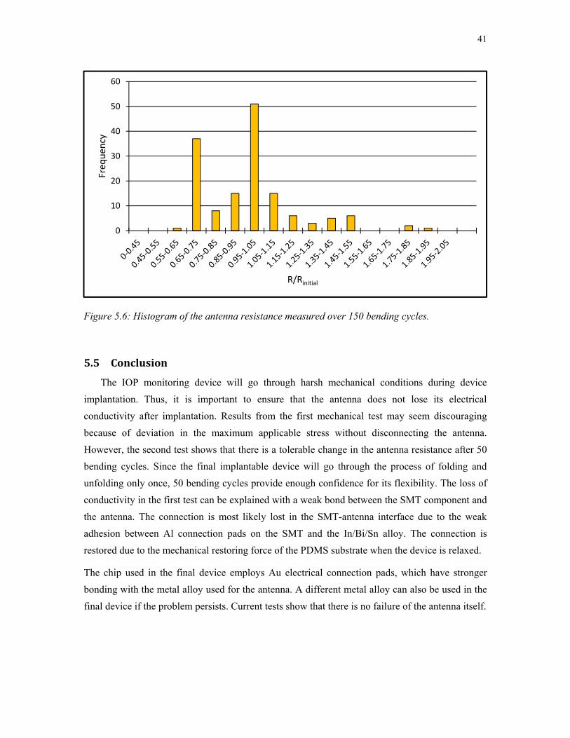
41
Figure 5.6: Histogram of the antenna resistance measured over 150 bending cycles.
5.5 Conclusion
The IOP monitoring device will go through harsh mechanical conditions during device
implantation. Thus, it is important to ensure that the antenna does not lose its electrical
conductivity after implantation. Results from the first mechanical test may seem discouraging
because of deviation in the maximum applicable stress without disconnecting the antenna.
However, the second test shows that there is a tolerable change in the antenna resistance after 50
bending cycles. Since the final implantable device will go through the process of folding and
unfolding only once, 50 bending cycles provide enough confidence for its flexibility. The loss of
conductivity in the first test can be explained with a weak bond between the SMT component and
the antenna. The connection is most likely lost in the SMT-antenna interface due to the weak
adhesion between Al connection pads on the SMT and the In/Bi/Sn alloy. The connection is
restored due to the mechanical restoring force of the PDMS substrate when the device is relaxed.
The chip used in the final device employs Au electrical connection pads, which have stronger
bonding with the metal alloy used for the antenna. A different metal alloy can also be used in the
final device if the problem persists. Current tests show that there is no failure of the antenna itself.
0
10
20
30
40
50
60
Freq
uen
cy
R/Rinitial

42
CHAPTER 6. PRESSURE MEASUREMENT
6.1 Introduction
The final step in device characterization is pressure sensor testing. This step includes both wired
and wireless pressure measurement experiments. The pressure sensor is first tested for the effect
of the PDMS coating on sensor reading and sensitivity. Later, the device prototype is used for
wireless pressure measurement inside a controlled pressure chamber.
6.2 EffectofPDMSCoatingonPressureSensor
The effect of PDMS coating on pressure sensor performance is studied before device integration.
A Cr/Au metal layer is patterned on a glass substrate with a lift-off process. The capacitive
pressure sensor is wire-bonded to the Cr/Au layer. It is placed into a pressure chamber where
pressure is varied between 0.3-1 bar. Capacitance is monitored with a Hewlett-Packard 4263A
LCR Meter at 100 kHz and 50mV bias. Later, a 50-m thick PDMS layer is spin-coated on the
sensor and cured at 60°C. Sensor response is recorded in the same pressure interval after the
spin-coating. The sensor is left to reach a steady state for 5 minutes at each measurement step.
The result is plotted with respect to the sensor reading at atmospheric pressure in Figure 6.1. This
reference capacitance is 18.28 pF without the PDMS coating and increases to 20.93 pF with the
coating. The average sensitivity of the sensor is measured as 0.60 pF/bar initially, increasing to
0.69 pF/bar after the coating. Figure 6.2 presents the amount of change in the sensor capacitance
due to the PDMS coating. The maximum change occurs around 0.35 with 0.5%.
The change in capacitance due to the added PDMS mass can be calculated using pressure applied
by that mass. It is calculated as 0.47 Pa (4.7 × 10⁻⁶ bar) for a 50 μm-thick PDMS layer using
equation (6.1). The pressure due to the PDMS coating is insignificant compared to pressure
values in the test.
(6.1)
P: pressure
t: thickness of the coating
d: density of the coating
g: gravity
Added PDMS layer does not alter the pressure sensing characteristics. The reason for the slight
increase in the sensor capacitance and sensitivity are unknown at this stage. Parasitic charges
introduced to the system should be considered.

43
Figure 6.1: Pressure sensor reading before and after PDMS coating. Error bars show the
uncertainty in capacitance due to LCR meter.
Figure 6.2: Amount of change in pressure sensor capacitance with PDMS coating.
0.97
0.975
0.98
0.985
0.99
0.995
1
1.005
1.01
0.3 0.4 0.5 0.6 0.7 0.8 0.9 1
C/C
reference
Pressure (bar)
With PDMS
Without PDMS
‐0.015
‐0.01
‐0.005
0
0.005
0.01
0.3 0.4 0.5 0.6 0.7 0.8 0.9 1
∆(C/C
reference)
Pressure (bar)

44
6.3 WirelessPressureMeasurement
Figure 6.3: Test setup for the wireless pressure measurement.
The setup illustrated in Figure 6.3 is used for wireless pressure measurements from the device
prototype. The device is placed in a pressure chamber, which is 1 cm away from the horn antenna.
The pressure inside the chamber is controlled by a valve connected to a pressurized air source.
The RF signal is transmitted to the device using the RF signal generator (E4438C ESG Vector
Signal Generator, Agilent Technologies) and the horn antenna to power the device. The
backscattered signal is isolated from the transmitted signal using a directional coupler (Krytar,
4080180) and analyzed with a spectrum analyzer (RSA3408A Real-Time Spectrum Analyzer,
Tektronix). A Bosch BMP085 Barometric Pressure Sensor is installed into the pressure chamber
as a reference. In each pressure step, the sensor is left to reach a steady state for 5 minutes.

45
Figure 6.4: Above: Change in with increased pressure. Below: Frequency spectrum for
each data point.
16.65
16.7
16.75
16.8
16.85
16.9
16.95
0 2 4 6 8 10 12 14 16
∆f p(kHz)
Pressure (mm‐Hg)
A
B
C

46
The RF chip used in the device is operated in reference capacitor transmission mode and pressure
transmission mode for the wireless pressure measurement via an I2C connection (Aardvark
I2C/SPI Host Adapter, Total Phase Inc.) to the prototype. Two frequency components, carrier
frequency ( ) and deviation in frequency due to the measurement result (∆ R, ∆ P), are observed.
The difference between the two frequencies (Δ ) is linearly related to the measured pressure
according to equation (6.2) in pressure measurement mode.
∆ R
∆ Po (6.2)
: Pressure-frequency shift coefficient
o: Offset pressure
Δ , Δ and pressure from BMP085 is recorded at each measurement step. Results are plotted
in Figure 6.4. Δ is recorded as 12.75 kHz in all steps. and o are calculated as –61.32 and
1038.4 after line fitting. Averaged sensitivity is calculated as 16.66 Hz/mm-Hg.
Three data points obtained from the device are encouraging but not enough to claim device
operation in the intended pressure interval. Unfortunately, there are several problems observed
during the pressure measurement. First of all, the chip is not set to the intended configuration all
the time. The operation mode of the chip is decided according to the frequency of the
backscattered signal. The configuration bit stream is sent to the device several times before a
backscattered signal is obtained. However, it is lost within a few seconds of the RF chip
configuration. The signal is restored for another few seconds upon re-sending the chip
configuration bit stream. These phenomena are observed consistently in three prototype devices.
A writing error in the chip serial interface can explain the observed behavior. A defect or defects
in the shift register, either due to the chip fabrication or device integration process, might be the
cause. The I2C connection is continuously monitored for signal waveforms and timings of the
clock and configuration bit streams to ensure transmission of the correct bit sequence. Board
connections and pressure sensor capacitance are also checked to eliminate any failure due to
those.
It is observed that the chip is harvesting RF power and temporarily backscattering the measured
parameter. The same behavior is also observed in the temperature and reference capacitor modes.
Thus, it is concluded to be a configuration interface problem rather than a pressure sensing
problem.

47
6.4 Conclusion
The presented test results show that PDMS coating has a tolerable effect on the capacitive
pressure sensing characteristics. It increases the device capacitance as well as sensitivity.
However, those changes are relatively small and do not alter the device response. The observed
effects can be attributed to the dielectric nature of the coating. It is also seen that the prototype is
capable of capturing the pressure information and transmit it to the outside receiver while it is
powered wirelessly. However, continuous pressure measurement in the 0-30 mmHg interval is
not observed due to the chip configuration problem described in the previous section. Further
research is needed to figure out the root-cause of the problem.

48
CHAPTER 7. CONCLUSIONS AND FUTURE WORK
7.1 Conclusions
The focus of this dissertation is an intraocular pressure monitoring device, which is implanted
during cataract surgery. A novel fabrication and packaging method for the monitoring device is
introduced. A device prototype is fabricated. Throughout comprehensive modeling and
systematic tests, device functionality is demonstrated.
The device illustrated in Figure 2.2 will be embedded in a capsular tension ring like structure in
order to be integrated into cataract surgery. Results obtained from three fabrication methods
indicate that the solder-filled-microchannel approach is promising for fabrication of the desired
IOP sensor as well as other flexible structures. It can fabricate thick metal structures on a flexible
substrate without electroplating and at a relatively low process temperature of 75 °C. The
presented process achieves the antenna fabrication and the chip integration in a single step.
Additionally, heat-assisted repair of broken metal structures is presented.
A device prototype is introduced and fabricated using the solder-filled microchannel process
(Figure 3.5). The device is first assembled on a PCB, then successfully embedded into PDMS and
integrated with the antenna. The presented method can be used for biocompatible packaging of
microsystems and sensors.
The prototype is tested for wireless power and data transfer. Results indicate that it can be
powered wirelessly from up to 2 cm distance (Figure 4.2). Calculated electromagnetic power
density on the tissue surface is below the maximum permissible exposure limit. Data transfer is
proven through the backscattered signal for the programmed chip mode (Figure 4.5). Each mode
is clearly visible in the frequency spectrum of the received signal.
Mechanical flexibility of the antenna is tested using a mockup device. Results show that the
antenna is conductive up to a mechanical stress of 33 kPa. Connection is lost momentarily at
higher stress levels, up to 116 kPa. However, connection is restored upon release of the stress.
Test results indicate a tolerable change in the antenna resistance after 50 bending cycles.
The effect of PDMS coating on the pressure sensor is tested. Results show an acceptable increase
in capacitance and sensitivity. Wireless pressure measurements are performed with the prototype
(Figure 6.4). Results indicate a pressure sensitivity of 16.66 Hz/mm-Hg. However, continuous
pressure monitoring in the interval of 0-30 mmHg is not performed due to problems in the chip
configuration step.
The prototype presents complete device functionality. Results are promising towards building a
complete wireless IOP monitoring device, which can be implanted during a cataract surgery.

49
7.2 FutureWork
7.2.1 TestinginanEyeModel
The effect of environmental variables on device performance should be analyzed. The presented
test results show the device functionality in air. However, the device will be implanted into the
anterior chamber, in a liquid environment surrounded by layers of tissue. Added layers will cause
attenuation in transferred power and received signal levels. The transmitted power level needs to
be increased to overcome those while keeping tissue surface radiation below the maximum
permissible exposure limit. The amount of attenuation depends on the transmission distance and
conductivity of the medium.
Environmental tests can be performed in two steps:
Testing in water: The prototype will be located in a solution similar to aqueous humor in
content (mostly water, saline, glucose, proteins, aminoacids, etc.). Wireless power
transfer and pressure measurements will be performed.
Testing in eye model: The prototype will be placed into an eye model, which
incorporates the fluid in the previous test with a layer of tissue representing the cornea.
Wireless power transfer and pressure measurements will be performed.
The antenna design can be changed to improve the antenna gain if transmission problems are
observed.
7.2.2 FromPrototypetoaCompleteDevice
Operation of the device prototype is presented with systematic testing in this dissertation. Results
are encouraging to move from prototyping to a complete device. However, the device size is
relatively large due to the PCB. This requires redesign of the RF chip to accommodate the
following:
All SMT components except an SMT capacitor should be removed in the final device.
The wired connection needed for chip configuration should be removed. Parameters
determining the chip operation are configured using a wired connection in the prototype
in order to determine the most suitable configuration. Chips can be preset to this
configuration during the design. Or, they can be configured wirelessly through an RF
signal.
An IOP monitoring device fabricated with the redesigned chip will have a footprint which can be
embedded in the capsular tension ring like implant. Thus, in vivo testing will be possible.
7.2.3 SalinityandpHMonitoring
Using an active implanted device also enables monitoring additional health parameters. The

50
presented prototype can be considered as a platform where monitored parameter or parameters
depend on the integrated sensor or sensors. Thus, it can be used for building a battery-less body
area network for health monitoring. Bearing that in mind, expansion on the sensing capability
should be considered.
Salinity and pH sensors can be added to the prototype in order to observe their effect on IOP and
glaucoma. Preliminary studies on salinity and pH measurements are performed using impedance
spectrometry. The setup in Figure 7.1 is used for salinity and pH measurements. The
electrochemical cell can be modeled using two resistors and a capacitor. When AC voltage at
high frequency is applied to the electrochemical cell, the double layer capacitance can be
approximated like a short circuit and the resistance of the solution can be measured. This
resistance is strongly dependent on the ion concentration in the solution. For the proposed salinity
sensor, an AC voltage at 10 kHz is applied to the given electrochemical cell and the current is
measured. The resistance is calculated as the ratio of the two values.
Figure 7.1: Setup used for salinity and pH measurements, and its circuit representation. Re:
resistance due to the redox reactions on the electrodes. Rw: resistance of the solution. Cdl:
capacitance due to the double layer formation around the electrodes.
Results are plotted in Figure 7.2 and Figure 7.3. Considerable resistance change is obtained with
the change in NaCl concentration. However, there is also a strong correlation with pH levels. A
measurement method which can isolate pH levels from NaCl concentration should be developed.
A drawback of the resistive sensing is an increase in power consumption. That can be prohibitive
for limited power budget applications.

51
Figure 7.2: Change in solution resistance with NaCl concentration. pH is kept constant in this
measurement.
Figure 7.3: Change in solution resistance due to change in pH and NaCl concentration.
A low-power pH and NaCl concentration sensing method needs to be developed. The expansion
of platform capabilities can be achieved by the integration of this method into the existing
prototype. That may lead to an implanted multi-sensor platform, which can revolutionize the
diagnosis tools.
60.00
80.00
100.00
120.00
140.00
160.00
180.00
200.00
110.00 120.00 130.00 140.00 150.00 160.00 170.00
Resistance (Ohm)
NaCl concentration (mM)
60.00
70.00
80.00
90.00
100.00
110.00
120.00
6.60 6.80 7.00 7.20 7.40
Resistance (Ohm)
pH
130 mM
140 mM
150 mM

52
REFERENCES
1. Kingman, S., Glaucoma is second leading cause of blindness globally. Bulletin of
the World Health Organization, 2004. 82(11).
2. Quigley, H.A. and A.T. Broman, The number of people with glaucoma worldwide
in 2010 and 2020. The British Journal of Ophthalmology, 2006. 90(3): p. 262-7.
3. Hughes, E., P. Spry, and J. Diamond, 24-hour monitoring of intraocular pressure
in glaucoma management: a retrospective review. American Journal of
Ophthalmology, 2004. 137(1).
4. Rosengren, L., et al., A system for passive implantable pressure sensors. Sensors
and Actuators. A, Physical., 1994. 43(1/3): p. 55.
5. Schnakenberg, U., et al., Initial investigations on systems for measuring
intraocular pressure. Sensors and Actuators. A, Physical., 2000. 85(1): p. 287.
6. Stangel, K., et al., A programmable intraocular CMOS pressure sensor system
implant. IEEE Journal of Solid-State Circuits, 2001. 36(7): p. 1094-1100.
7. Chen, P.-J., et al., Unpowered spiral-tube parylene pressure sensor for
intraocular pressure sensing. Sensors and Actuators A: Physical, 2006. 127(2): p.
276-282.
8. Chen, P.J., et al., Microfabricated implantable parylene-based wireless passive
intraocular pressure sensors. Journal of Microelectromechanical Systems, 2008.
17(6): p. 1342-1351.
9. Haque, R.M. and K.D. Wise. A 3D implantable microsystem for intraocular
pressure monitoring using a glass-in-silicon reflow process. in IEEE 24th
International Conference on Micro Electro Mechanical Systems (MEMS). 2011.
10. Chitnis, G.D., et al. An ocular tack for minimally invasive continuous wireless
monitoring of intraocular pressure. in IEEE 25th International Conference on
Micro Electro Mechanical Systems (MEMS). 2012.
11. Leonardi, M., et al., First steps toward noninvasive intraocular pressure
monitoring with a sensing contact lens. Invest. Ophthalmol. Vis. Sci., 2004. 45(9):
p. 3113-7.
12. Leonardi, M., et al., Wireless contact lens sensor for intraocular pressure
monitoring: assessment on enucleated pig eyes. Acta. Ophthalmol, 2009. 87(4): p.
433-7.
13. Shih, Y.C., B.P. Otis, and T. Shen, A 2.3 μW wireless intraocular
pressure/temperature monitor. IEEE Journal of Solid-State Circuits, 2011. 46(11):

53
p. 2592-2601.
14. Bae, B., et al., Design optimization of a piezoresistive pressure sensor considering
the output signal-to-noise ratio. Journal of Micromechanics and Microengineering,
2004. 14(12): p. 1597-1607.
15. Bae, B., K. Park, and M.A. Shannon, Low-pressure treatment control of
glaucoma using an electromagnetic valve actuator with a piezoresistive pressure
sensor. 2005: p. 126-129.
16. Chen, P.J., et al., Implantable Unpowered Parylene MEMS Intraocular Pressure
Sensor. in International Conference on Microtechnologies in Medicine and
Biology. 2006.
17. Chen, P.-J., et al., Wireless Intraocular Pressure Sensing Using Microfabricated
Minimally Invasive Flexible-Coiled LC Sensor Implant. Journal of
Microelectromechanical Systems, 2010. 19(4).
18. Leonardi, M., et al., Wireless contact lens sensor for intraocular pressure
monitoring: assessment on enucleated pig eyes. Acta Ophthalmologica, 2009.
87(4).
19. Stangel, K., et al., A Programmable Intraocular CMOS Pressure Sensor System
Implant. IEEE Journal of Solid-State Circuits., 2001. 36(7): p. 1094.
20. Dosso, A.A., et al., Outcomes of coaxial microincision cataract surgery versus
conventional coaxial cataract surgery. J Cataract Refract. Surg., 2008. 34(2): p.
284-8.
21. Krupin, T. Feitl, and M.E. Bishop, Postoperative intraocular pressure rise in
open-angle glaucoma patients after cataract or combined cataract-filtration
surgery. OPHTHA Ophthalmology, 1989. 96(5): p. 579-584.
22. Siegel, A.C., et al., Cofabrication of electromagnets and microfluidic systems in
poly(dimethylsiloxane). Angewandte Chemie, International Edition, 2006. 45(41):
p. 6877-6882.
23. Siegel, A.C., et al., Microsolidics: Fabrication of Three-Dimensional Metallic
Microstructures in Poly(dimethylsiloxane). Advanced Materials., 2007. 19(5): p.
727-733.
24. Siegel, A.C., et al., Cofabrication: A Strategy for Building Multicomponent
Microsystems. Accounts of Chemical Research, 2010. 43(4): p. 518-528.
25. Wei, P., et al., Stretchable microelectrode array using room-temperature liquid
alloy interconnects. Journal of Micromechanics & Microengineering, 2011. 21(5).
26. Surapaneni, R., et al. Self-Healing Microfluidic Wires For Ultra-Reliable Flexible
Microsystems. in 15th International Conference on Miniaturized Systems for

54
Chemistry and Life Sciences. 2011. Seattle, Washington, USA.
27. Armani, D., C. Liu, and N. Aluru. Re-configurable fluid circuits by PDMS
elastomer in Twelfth IEEE International Conference on micromachining. in
Micro Electro Mechanical Systems (MEMS). 1999.
28. Wen, L., et al., A Parylene temporary packaging technique for MEMS wafer
handling. Sensors & Actuators: A. Physical, 2012. 186: p. 289-297.
29. Gutierrez, C.A. and E. Meng, Parylene-based electrochemical-MEMS
transducers. Journal of Microelectromechanical Systems, 2010. 19(6): p.
1352-1361.
30. Po-Jui, C., et al., Microfabricated Implantable Parylene-Based Wireless Passive
Intraocular Pressure Sensors. Journal of Microelectromechanical Systems, 2008.
17(6): p. 1342-1351.
31. Hassler, C., T. Boretius, and T. Stieglitz, Polymers for neural implants. Journal of
Polymer Science, Part B: Polymer Physics, 2011. 49(1): p. 18-33.
32. Lago, N., et al., Long term assessment of axonal regeneration through polyimide
regenerative electrodes to interface the peripheral nerve. Biomaterials., 2005.
26(14): p. 2021-2031.
33. Richardson, R.R., J.A. Miller, and W.M. Reichert, Polyimides as biomaterials:
preliminary biocompatibility testing. Biomaterials, 1993. 14(8): p. 627-635.
34. Jung, I., et al., Dynamically tunable hemispherical electronic eye camera system
with adjustable zoom capability. Proceedings of the National Academy of
Sciences of the United States of America, 2011. 108(5): p. 1788-1793.
35. Kim, D.-H., et al., Materials and noncoplanar mesh designs for integrated
circuits with linear elastic responses to extreme mechanical deformations.
Proceedings of the National Academy of Sciences of the United States of
America., 2008. 105(48): p. 18675.
36. Sun, Y., et al., Controlled buckling of semiconductor nanoribbons for stretchable
electronics. Nat Nanotechnol, 2006. 1(3): p. 201-7.
37. Chang, J.H.C., et al., High yield packaging for high-density multi-channel chip
integration on flexible parylene substrate. Proceedings of the IEEE International
Conference on Micro Electro Mechanical Systems (MEMS), 2012: p. 353-356.
38. Po-Jui, C., et al. Implantable parylene-based wireless intraocular pressure sensor.
in IEEE 21st International Conference on Micro Electro Mechanical Systems
(MEMS). 2008.
39. Po-Jui, C., et al., Wireless Intraocular Pressure Sensing Using Microfabricated
Minimally Invasive Flexible-Coiled LC Sensor Implant. Journal of

55
Microelectromechanical Systems, 2010. 19(4): p. 721-734.
40. Gonenli, I.E., Z. Celik-Butler, and D.P. Butler, Surface micromachined MEMS
accelerometers on flexible polyimide substrate. IEEE Sensors Journal, 2011.
11(10): p. 2318-2326.
41. Suh, J.W., et al., Fully programmable MEMS ciliary actuator arrays
formicromanipulation tasks. Proceedings of the IEEE International Conference on
Robotics and Automation , 2000. 2: p. 1101-1108.
42. Bashir, R., et al., Micromechanical cantilever as an ultrasensitive pH microsensor.
Applied Physics Letters, 2002. 81(16): p. 3091.
43. Lee, K.J., K.A. Fosser, and R.G. Nuzzo, Fabrication of Stable Metallic Patterns
Embedded in Poly(dimethylsiloxane) and Model Applications in Non-Planar
Electronic and Lab-on-a-Chip Device Patterning. Advanced Functional
Materials., 2005. 15(4): p. 557.
44. Bowden, N., et al., Spontaneous formation of ordered structures in thin films of
metals supported on an elastomeric polymer. Nature, 1998. 393(6681).
45. Chen, X. and J.W. Hutchinson, Herringbone Buckling Patterns of Compressed
Thin Films on Compliant Substrates. Journal of Applied Mechanics, 2004. 71(5).
46. Han-Sheng, C. and W. Steven, Design, fabrication and characterization of a
conducting PDMS for microheaters and temperature sensors. Journal of
Micromechanics and Microengineering, 2009. 19(4).
47. IEEE Standard for Safety Levels With Respect to Human Exposure to Radio
Frequency Electromagnetic Fields, 3 kHz to 300 GHz. IEEEStd. C95.1, 2006.