fluidics and dna - lth · pdf fileand fabrication of a working device and ... a single...
TRANSCRIPT

I
II
Fluidics and DNA Guidance in Hollow
NanoWires
Report for Master Thesis (30 hp)
Division of Solid State Physics Department of Physics
Lund University
Farnaz Yadegari 19 December 2011
Supervisors: Jonas O.Tegenfeldt, Heiner Linke Henrik Persson

III
AFM Atomic Force Microscopy
ALD Atomic Layer Deposition
AlInP Aluminium Indium Phosphide
Al2O3 Aluminium Oxide
Ar Argon
BME 훽-Mercaptoethanol
Cr Chromium
DI water De-Ionized water
DNA Deoxyribonucleic acid
EBL Electron Beam Lithography
FIB Focused Ion Beam
GaAs Gallium Arsenide
GaP Gallium Phosphide
Ga(CH3)3 Trimethylgallium
HNW Hollow NanoWire
H2O2 Hydrogen peroxide
H SO Sulphuric acid
IPA Isopropyl Alcohol
LMIS Liquid Metal Ion Source
MOVPE Metal Organic Vapour Phase Epitaxy
MWCNT Multi Wall Carbon Nano Tube
NW Nano Wire
PDMS Polydimethylsiloxane
PMMA Polymethylmethacrylate
PVD Physical Vapour Deposition
PVP Polyvinylpyrrolidone
RIE Reactive Ion Etching
SEM Scanning Electron Microscopy
TBE Tris Borate Sodium EDTA
TMA Trimethylaluminium
UVL UV Lithography
VPE Vapour Phase Epitaxy
λ-DNA Lambda-phage DNA

IV
V
Abstract
Hollow nanowires (HNWs) consisting of inorganic tubes of an inner diameter of 10-80 nm, outer diameter of 50-200 nm and length of several µm are outstanding candidates both for applications involving direct chemical access to the cytosol of living cells and for investigations of basic transport phenomena. A device has been fabricated in which HNWs, lying on a glass surface, are connected to microfluidic channels for the purpose of guiding DNA and to characterize the fluidic properties of the HNWs. The HNWs are aligned individually on a substrate by a combination of electron beam lithography and mechanical force.
My contribution to this project has been to align the HNWs with sub-µm precision, the design and fabrication of a working device and the test of the fluidic properties of the nanowires with DNA. According to the observations, HNWs are not clogged by resist; however, further considerations must be made for proper sealing of the device in order to observe transport of DNA through the wires.
Keywords:
Hollow nanowires, microfluidics connections

VI
Acknowledgments
First of all I would like to thank my supervisors Jonas O. Tegenfeldt and Heiner Linke who gave me this opportunity to work on this project. I am incredibly grateful for all feedback and ideas I have received during our meetings and discussions. I also appreciate the opportunity that Jonas gave me to present my work at Microtas 2011 in Seattle.
I would like also to thank Henrik Persson, who made the HNWs and was my direct supervisor in this project. Without his help it would not have been easy to find the correct way especially in characterization of the devices and fluorescence microscopy.
Mercy Lard is acknowledged for helping me to learn how to work with different machines and for always spending time to check the fabrication results.
Jason Beech and Cassandra Niman who always had some great suggestions and answers for my problems and questions.
I would like to thank the Lund Nano Labs staff and the entire bionano group for an enjoyable working environment.
Last but not least my family, Majid and Bahar for all their support and encouragement.

1
ABSTRACT ........................................................................................................................................................ V
ACKNOWLEDGMENTS ..................................................................................................................................... VI
1. INTRODUCTION ............................................................................................................................................ 3
1.1 MICROFLUIDICS AND NANOFLUIDICS ................................................................................................................. 3 1.2 CELL INJECTION ........................................................................................................................................... 4
2. MICRO AND NANO FABRICATION ................................................................................................................. 8
2.1 TOOLS FOR CREATING HOLLOW NANOWIRES ....................................................................................................... 8 NANOWIRES GROWTH USING MOVPE ................................................................................................................... 8 ATOMIC LAYER DEPOSITION (ALD) WITH ALUMINIUM OXIDE ........................................................................................ 9 ARGON SPUTTERING AND OXYGEN PLASMA ETCHING .................................................................................................. 9 WET ETCHING ................................................................................................................................................ 10 2.2 TOOLS FOR DEVICE FABRICATION ................................................................................................................... 10 UV LITHOGRAPHY AND DIFFERENT RESISTS ............................................................................................................. 10 EVAPORATION (METALLIZATION) ......................................................................................................................... 11 LIFT OFF ....................................................................................................................................................... 11 ELECTRON BEAM LITHOGRAPHY AND DIFFERENT RESISTS ............................................................................................ 12 2.3 DEVICE CHARACTERIZATION .......................................................................................................................... 13 ELECTRON MICROSCOPY.................................................................................................................................... 13 FOCUSED ION BEAM (FIB) ................................................................................................................................. 14 FLUORESCENCE MICROSCOPY ............................................................................................................................. 14
3. DEVICE FABRICATION ................................................................................................................................. 16
3.1 PROCESSING............................................................................................................................................. 17 THE WORK ON OUR NWS.................................................................................................................................. 17 DEFINITION OF ALIGNMENT MARKS WITH UVL AND METALLIZATION ............................................................................ 20 BREAKING AND TRANSFERRING THE HNWS ........................................................................................................... 21 ALIGNMENT OF THE HNWS ............................................................................................................................... 21 UVL ON SU8................................................................................................................................................. 23 SEALING THE DEVICES ....................................................................................................................................... 24 3.2 CHARACTERIZATION ................................................................................................................................... 24
4. RESULTS ..................................................................................................................................................... 25
4.1 CREATION OF HOLLOW NANOWIRES ............................................................................................................... 25 4.2 ALIGNMENT OF HOLLOW NANOWIRES ............................................................................................................. 26 4.3 CREATION OF MICROCHANNELS SEPARATED BY A WALL ON TOP OF THE HNWS .......................................................... 29 4.4 FOCUSED ION BEAM ................................................................................................................................... 29 4.5 SEALING .................................................................................................................................................. 30 4.6 DNA INJECTION ........................................................................................................................................ 31
5. TECHNICAL SUMMARY ............................................................................................................................... 35
6. CONCLUSION AND OUTLOOK ..................................................................................................................... 39
BIBLIOGRAPHY ............................................................................................................................................... 41
APPENDIX A ................................................................................................................................................... 44
HNW FABRICATION......................................................................................................................................... 44 FABRICATION OF MICROFLUIDIC CONNECTIONS ....................................................................................................... 45
APPENDIX B .................................................................................................................................................... 47

2
THICKNESS TEST .............................................................................................................................................. 47 HEIGHT TEST OF ALIGNED HNWS ........................................................................................................................ 47
APPENDIX C .................................................................................................................................................... 49
ABSTRACT AND POSTER AT MICROTAS 2011 (2-6 OCTOBER, SEATTLE, USA) ................................................................ 49

3
1. Introduction The aim of this project was the fabrication of a device with horizontal Hollow Nanowires (HNWs) on the surface of the substrate to develop fluidics and studying the guidance of DNA through HNWs. In this section I will explain why this can be important for bionano applications, in particular.
1.1 Microfluidics and nanofluidics
The behaviour of a fluid in a system with dimensions of around tens to hundreds of micrometers is completely different from conventional flow theory. A new method of engineering and controlling of such a system was developed in the late 1980s: “microfluidics.” Almost three decades after the miniaturization of electronic devices began, the fluidic and optical components were utilized in microsystems. Microflow sensors, micropumps and microvalves were developed as the first generation of microdevices. Microfluidics has opened a new window for the size reduction of devices and has changed analysis of experiments due to the possibility of using small amounts of reagents. It also has shown high sensitivity for detection and separation, higher throughput and lower experiment cost [1].
Microfluidics has influenced different fields of science, but molecular biology has been affected by microfluidics most strongly. In turn microfluidics is affected by microelectronics methods both in fabrication and application.
Photolithography and other micro- and nanofabrication techniques on silicon and glass have been applicable in microfluidics. New materials, such as plastics, have offered unique characteristics to microfluidics. Using new fabrication techniques, essential components of microsystems such as pipes and mixers can be produced on small chips that require different components and subsystems [2].
In general, the advantages of microfluidics in different fields can be summarized as follows: improved data quality, fewer experiments required, reduction of reagent consumption, shorter reaction times, better performance, higher throughput due to parallel processes and reduction of costs [3].
In nanotechnology, nanofluidics can be defined as the study and application of fluidics transport at the nanometer-scale [4]. Although there are some differences between fluid behaviour in micro and nano scale, in some way nanofluidics can be considered as the next generation of microfluidics.
The development of novel nano structures became possible due to new nanofabrication techniques. Nowadays, nanofluidics devices are applicable in biology for analysis, separation, concentration, manipulation and detection of biomolecules. Sensitivity and throughput are two important factors, which are improved in such devices [5].
4
Nanofluidics exist in many classical disciplines of science such as biology (physiology and genetics), physics (physics of fluids, thermodynamics, surface science and tribology), chemistry (separation science, polymer science and colloid chemistry), engineering (microengineering and bioengineering) and membrane science [4].
1.2 Cell injection
Delivering biomolecules into cells or to a desired place in an in-vitro environment has been a challenge for several years. Protein, DNA, RNA, and small biomolecules have been delivered into living cells by classical chemical transfection methods. These methods, which are based commonly on lipids and calcium phosphate precipitation, suffer from inefficiency and show toxicity problems for living cells [6]. Delivering the genetic material and antibodies using viral vectors and liposome respectively is also reported [7], [8].
In this way, development of new delivery and injection devices based on micro, and nanofluidics is an important area of research in molecular biology and nanotechnology.
Microfluidics systems – networks of different components such as pumps, valves, mixers and separators- are applicable to chemical analysis of cells [9], protein and DNA separation [10], [11], cell sorting [12] and delivering both biomolecules and drugs [3], [13].
Microfluidics can be useful in the control of cell position for the purpose of induction pattern formation. Pattern formation is defined as the design and control of the biochemical composition, topology of the substrate, the medium composition and the types of cells in the vicinity of each other. The main idea is based on the possibility of delivering a precise amount of cell binding agents, proteins, for example, to specific regions on the substrate using microfluidics systems[14], [15].
Delivering biomolecules by different nanowires and nanotubes has been reported by several groups. Fabrication of a “nanoinjector” based on carbon nanotubes that can penetrate the cell membrane with minimum perturbation is reported by Chen et al. This nanoinjector can also be used for cargo delivery to a cell’s interior [16]. In this work, a single multiwall carbon nanotube (MWCNT) is connected to the tip of an atomic force microscope (AFM) and serves as a nanoneedle. To enable simultaneous fluorescence microscopy, the AFM is connected to an inverted fluorescence microscope. They used MWCNT for loading cargo and releasing it to the interior of cells (figure 1).

5
Figure 1: (A) SEM image of a MWCNT-AFM tip,(B) TEM image of the tip region of(A), (C)SEM image of a
MWCNT-AFM tip coated with desired cargo (Q-Dot streptavidin) (16)
The use of vertical arrays of silicon nanowires for delivering different types of biomolecules into living cells is reported by Shalek et al. [17]. Figure 2 shows that in their work, biomolecules are efficiently delivered into spatially localized immortalized and primary mammalian cells.
Figure 2 : (A) and (B) SEM images of vertical Si nanowires (scale bars 1 µm), (C) confocal microscope section of a HeLa cell after 15 min and (D) after an hour, (E) scanning electron micrograph of rat hippocampal neurons
atop a bed of Si NWs (artificial colors) images are rearranged from (17). The main idea of delivering by solid nanowires is the binding the molecules to the surface of nanowires and releasing them inside the cells. By using hollow nanowires, these allow the

6
possibility of transportation from their core area without relying on cycle of the binding and release of molecules to the surface.
The use of freestanding HNWs as a nanotube membrane and flow through them has been reported recently. Sköld et al. have made one device in which GaAs-AlInP core-shell nanowires were grown by an epitaxial method on GaAs substrate and after the selective etching of the core and substrate the shell stands on the substrate as nanotubes with access from both sides of the membrane. Transport of DNA molecules was demonstrated through the nanowires using electrophoresis [18]. Some of the result of their work is presented in figure (3).
Figure 3: (A) and (B) TEM images of side and top view of hollow nanowires,(C) SEM image of nanowire membrane before substrate removal , (D) optical microscopy images of DNA electrophoresis through a
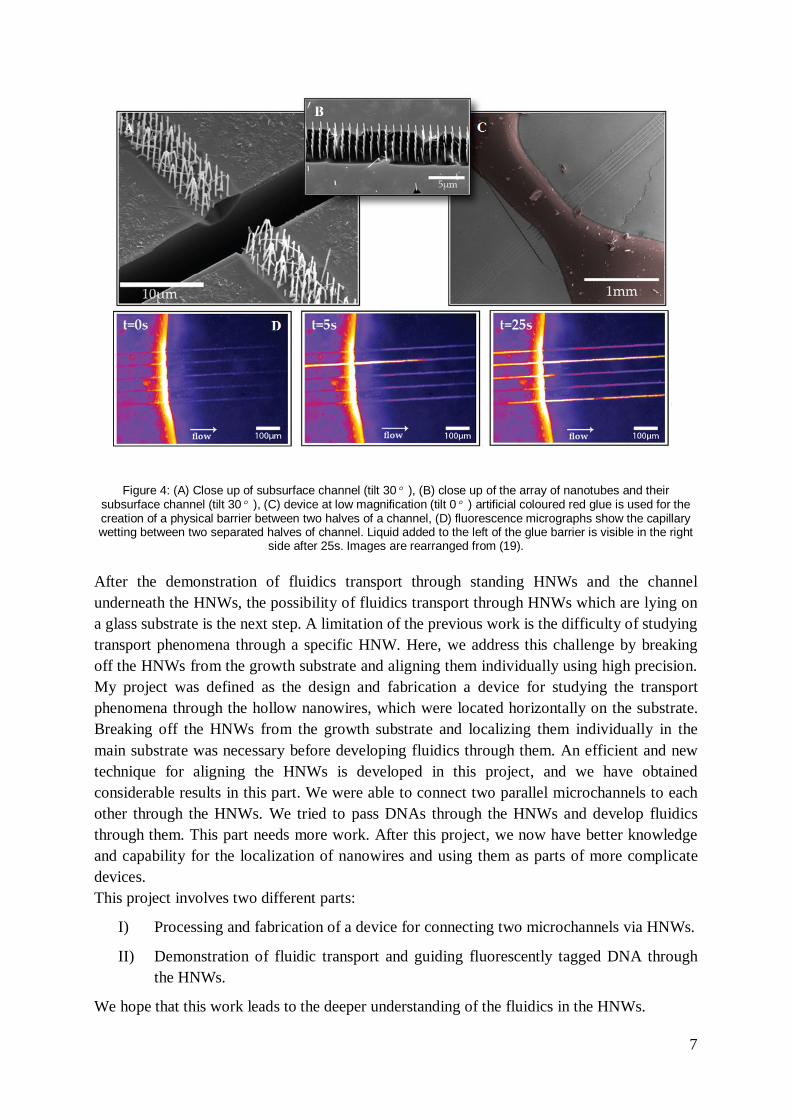
membrane at 0 V bias and (E) at 5 V bias. Images are rearranged from (18). Persson et al. have reported the fabrication of an array of vertical Al2O3 nanotubes, which are connected to subsurface microchannels and potentially applicable to cell injections. They have covered epitaxially grown GaP nanowires on the same substrate with Al2O3 by atomic layer deposition (ALD). Removing the tips of the oxide covered nanowires allows them to selectively etch the GaP core and substrate, which leads to the creation of an array of standing Al2O3 nanotubes, which are connected to each other from one side. As it shown in figure (4) Persson et al. have demonstrated fluidics transport in the underneath channel, and they hope to use the device for the successful injection of molecules into the cells [19].
7
Figure 4: (A) Close up of subsurface channel (tilt 30°), (B) close up of the array of nanotubes and their
subsurface channel (tilt 30°), (C) device at low magnification (tilt 0°) artificial coloured red glue is used for the creation of a physical barrier between two halves of a channel, (D) fluorescence micrographs show the capillary wetting between two separated halves of channel. Liquid added to the left of the glue barrier is visible in the right
side after 25s. Images are rearranged from (19). After the demonstration of fluidics transport through standing HNWs and the channel underneath the HNWs, the possibility of fluidics transport through HNWs which are lying on a glass substrate is the next step. A limitation of the previous work is the difficulty of studying transport phenomena through a specific HNW. Here, we address this challenge by breaking off the HNWs from the growth substrate and aligning them individually using high precision. My project was defined as the design and fabrication a device for studying the transport phenomena through the hollow nanowires, which were located horizontally on the substrate. Breaking off the HNWs from the growth substrate and localizing them individually in the main substrate was necessary before developing fluidics through them. An efficient and new technique for aligning the HNWs is developed in this project, and we have obtained considerable results in this part. We were able to connect two parallel microchannels to each other through the HNWs. We tried to pass DNAs through the HNWs and develop fluidics through them. This part needs more work. After this project, we now have better knowledge and capability for the localization of nanowires and using them as parts of more complicate devices. This project involves two different parts:
I) Processing and fabrication of a device for connecting two microchannels via HNWs.
II) Demonstration of fluidic transport and guiding fluorescently tagged DNA through the HNWs.
We hope that this work leads to the deeper understanding of the fluidics in the HNWs.

8
2. Micro and nano fabrication The creation of miniaturized structures and devices is completely related to available micro- and nanofabrication techniques. These techniques generally are divided into two main groups, top-down and bottom-up. Top-down techniques – like various kinds of lithography – are commonly used individually or in parallel for nano and microstructure patterning, while for the assembly of discrete nanoscale structures, the bottom-up techniques based on interactions between molecules or colloidal particles, are more common [20].
Some of the common techniques in micro and nanofabrication that are used in these experiments are briefly reviewed in this chapter, including the basics of the growth and processing of hollow nanowires.
Techniques applied for aligning HNWs, creating the channels on top of them and developing microfluidics through the device are reviewed in the following section.
2.1 Tools for creating hollow nanowires
Nanowires growth using MOVPE
Nanowires are grown using particle-assisted nanowire growth; this is one of the most important and commonly used categories of the metal organic vapour phase epitaxy (MOVPE) technique. MOVPE is, in turn, a subset of vapour phase epitaxy (VPE), which involves precipitation from a supersaturated vapour phase. MOVPE is a particular technique for some elements that cannot form stable hydrides or halides but can form stable metal organic compounds with reasonable vapour pressure. This vapour phase contains chemical precursors of the desired substrate. In MOVPE, a laminar gas flow of each precursor is achieved across the substrate surface by feeding each precursor individually into the reactor. The concentration gradient of materials on top of the substrate surface can lead and control the growth of the desired materials [21].
In particle-assisted nanowire growth, a liquid alloy of a metal particle (generally Au) and substrate is formed at temperatures higher than the eutectic temperature. The metal particle collects material from the vapour phase so that supersaturation and precipitation of the material occurs at the liquid-solid interface. In this condition, the metal particle acts as a catalyst or local seed and nanowires can grow underneath the metal particles. The diameter of the grown nanowires is controlled by the size of the metal particles. Gold aerosols or colloids are two well-known techniques for a homogeneous size distribution and also a controllable density of metal particles [22]. In this approach, the gold particles are randomly distributed over the surface. They can be ordered as arrays of particles using pattern-transferring techniques like electron beam lithography (EBL). Patterned sample allows us to position the nanowires and the possibility to study growth directions and diffusion effects [21].

9
For GaP nanowire growth, after deposition of the gold aerosol particles on GaP substrate, trimethylgallium, Ga(CH3)3 and phosphine PH3 flow in to the growth cell and GaP nanowires grow underneath the Au particles via this reaction:
Ga(CH3)3 + 푃퐻 → 퐺푎푃 + 3퐶퐻
Atomic layer deposition (ALD) with aluminium oxide
The greatest advantage of the ALD process is the ability to obtain uniform coverage of the substrate and great control of the thickness. To receive good deposition, the process relies on gaseous compounds that only deposit one atomic layer of film at a time. The sample is placed in a chamber and heated to 250°C and then exposed to trimethylaluminium (TMA). The TMA molecules adsorb on the surface with the methyl groups pointing upwards. This prevents further adsorption of TMA and effectively creates a monolayer of TMA. After this, the surplus TMA is removed from the chamber and water vapour is let in. This results in the formation of the metal oxide, in this case퐴푙 푂 , and enables further adsorption of TMA on the sample surface. For a 50-55 nm thick film, 500 cycles of the process are needed. These process steps enable precise control over the number of atomic layers that are deposited on the substrate [23].
Argon sputtering and oxygen plasma etching
The definition of sputtering is the bombardment and removal of atoms from the surface of a solid or target with energetic particles [24]. The removal of the solid film of resist is done by reactive ion etching (RIE), which is mostly chemical etching. In this technique, a chemical reaction occurs between resist molecules on the substrate and plasma ions to form a molecule that can be removed from the substrate. Although there is always some sputtering and physical etching, in most cases these effects are small and can be ignored [25]. RIE can be summarized as:
I) Creation of etchant species in the plasma (in this work oxygen plasma).
II) Transportation of reactant by diffusion and voltage attraction to the surface.
III) Adsorption of the reactive particle at the surface.
IV) Chemisorption of the reactive particle at the surface.
V) Formation of the product molecule.
VI) Desorption of the product molecule from the surface.
VII) Diffusion to the bulk gas and removal of the product molecule from the chamber by pumping.

10
Wet etching
Wet chemical etching is one of the most extensively used techniques in nanoprocessing. Most applications of wet etching are used for cleaning wafer surfaces before processing steps and to allow the controllable removal of material.
In wet etching techniques the substrate is usually immersed in the etching solution. Mechanical agitation and temperature are important factors for determining the etching rate.
2.2 Tools for device fabrication
UV lithography and different resists
UV lithography (UVL) is one of the most common techniques for pattern transfer to a solid substrate.
The sample, which is coated by a thin layer of photoresist, is exposed by ultraviolet light through a designed mask (commonly made of chromium on glass), which defines exposed and unexposed areas on the photoresist. After development, exposed or unexposed areas will be dissolved from the surface for positive and negative resist respectively. Diffraction limits the effective resolution and is a major limitation of UV lithography. On the other hand, UVL offers higher throughput than other lithography methods. Positive photoresist is made of a photosensitive compound, base resin and an organic solvent. After radiation, the chemical structure of the photosensitive component in the exposed area changes, and the resist is more soluble in developer solution so that exposed areas are removed after development.
Negative photoresists contain a polymer and a photosensitive compound. During exposure, polymer linking reactions occur due to the absorption of photons by the photosensitive compound leading to the cross linking of the polymer molecules. The cross linked polymers are less soluble in the developer solution because of their higher molecular weight so that unexposed areas are removed after development.
Patterns formed on the resist are either the same as the mask or reverse, corresponding to positive or negative photoresists [26] (figure 5). S1813 and SU-8 are examples of the positive and negative photoresist used in this project.

11
Figure 5: (A) Desired mask for UV lithography (dark part will not be exposed), (B)transferred pattern to the positive resist and(C) negative resist. In both samples (positive and negative resist) dark part shows remained resists on
substrate after exposure and development.
Evaporation (metallization)
Evaporation is categorized as a subgroup of physical vapour deposition (PVD), which is commonly used for sample coating and metallization. For evaporation, the source material must be heated up to its melting point and then the evaporated atoms travel at high velocity and are deposited on the substrate. Usually source materials are melted by resistive heating [26].
Lift off
Lift off is another important pattern transfer technique. In this technique, after transferring a pattern from mask to photoresist using lithography, a thin film (e.g. metal) is deposited on top of the resist and substrate (see evaporation above). An important point is that the film thickness should always be less than the resist thickness. For thick films, a double layer of resist can be used to ensure a discontinues metal layer. The film on top of the resists is removed after selectively removing the resist and the film, which is in direct contact with the substrate, remains and consequently, the substrate is patterned by the film material [26].
A
B
C
12
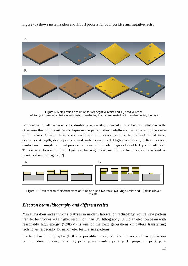
Figure (6) shows metallization and lift off process for both positive and negative resist.
Figure 6: Metallization and lift-off for (A) negative resist and (B) positive resist. Left to right: covering substrate with resist, transferring the pattern, metallization and removing the resist.
For precise lift off, especially for double layer resists, undercut should be controlled correctly otherwise the photoresist can collapse or the pattern after metallization is not exactly the same as the mask. Several factors are important in undercut control like: development time, developer strength, developer type and wafer spin speed. Higher resolution, better undercut control and a simple removal process are some of the advantages of double layer lift off [27]. The cross section of the lift off process for single layer and double layer resists for a positive resist is shown in figure (7).
Figure 7: Cross section of different steps of lift off on a positive resist. (A) Single resist and (B) double layer resists.
Electron beam lithography and different resists
Miniaturization and shrinking features in modern fabrication technology require new pattern transfer techniques with higher resolution than UV lithography. Using an electron beam with reasonably high energy (>20keV) is one of the next generations of pattern transferring techniques, especially for nanometer feature size patterns.
Electron beam lithography (EBL) is possible through different ways such as projection printing, direct writing, proximity printing and contact printing. In projection printing, a
A
B
A B
13
pattern is projected in parallel through a mask onto a resist-coated substrate by a relatively wide electron beam, which is controlled by a high precision electron lens system. In direct writing, there is no mask and the pattern is written on a resist-coated substrate by a small spot of the electron beam. Direct writing is the most common EBL since the complicated and expensive mask fabrication step is thus omitted [28].
Resists in EBL are polymers, which change chemically or physically upon irradiation by the electron beam. Like light sensitive resists, electron beam resists can be positive or negative [26].
2.3 Device characterization
The physical characterization of each device strongly relies on high-resolution techniques for imaging micro- and nanoscale structures after each processing step. Electron microscopy, focused ion beam (FIB) and fluorescence microscopy are used for characterization of our devices and are briefly summarized in this section.
Electron microscopy
Material science, semiconductor physics and modern biology are examples of different fields that heavily rely on electron microscopy techniques. Two examples of high resolution electron microscopy are transmission electron microscopy (TEM) and scanning electron microscopy (SEM). TEM requires very thin specimens and can produce two dimensional high resolution images. SEM gives slightly less resolution and is better for bulky specimens. It gives an impression of the three dimensional images of the specimen surface [29].
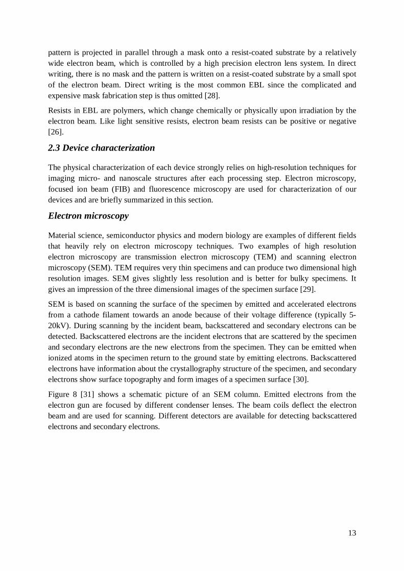
SEM is based on scanning the surface of the specimen by emitted and accelerated electrons from a cathode filament towards an anode because of their voltage difference (typically 5-20kV). During scanning by the incident beam, backscattered and secondary electrons can be detected. Backscattered electrons are the incident electrons that are scattered by the specimen and secondary electrons are the new electrons from the specimen. They can be emitted when ionized atoms in the specimen return to the ground state by emitting electrons. Backscattered electrons have information about the crystallography structure of the specimen, and secondary electrons show surface topography and form images of a specimen surface [30].
Figure 8 [31] shows a schematic picture of an SEM column. Emitted electrons from the electron gun are focused by different condenser lenses. The beam coils deflect the electron beam and are used for scanning. Different detectors are available for detecting backscattered electrons and secondary electrons.
14
Figure 8: Schematic picture of SEM column [31].
Focused ion beam (FIB)
When a solid is bombarded by an ion beam, kinetic energy is transferred from the ions to the solid surface. This energy transfer can lead to different phenomena, which may or may not be useful. Secondary electron emission and atomic sputtering are two of the most important and practically useful results of ion-solid interactions; focused ion beam (FIB) microscopy and milling are all based on them. While secondary electrons generated in this way can be used to obtain highly spatially resolved images, sputtering atoms from the surface of the substrate can lead to the milling of the sample. For both cases a highly focused ion beam is required.
The principle of the FIB instrument is more or less similar to the SEM with the difference that the sample is scanned using an ion beam instead of the electron beam. The most common ion source used in FIB instruments is a liquid metal ion source (LMIS), which provides the brightest and most highly focused beam. Gallium based LMIS is widely used in FIB instruments because of its low melting temperature, low volatility and low vapour pressure. In most FIB instruments, both a FIB column and a SEM column exist and consequently, both the removal and non destructive imaging are possible with this dual-beam platform instrument [32].
Fluorescence microscopy
Fluorescence microscopy in its various forms is probably one of the most powerful and commonly used optical techniques for biological applications.
Detection of the location of biological macromolecules and their response to environmental conditions are two parameters that can be studied by attaching a suitable fluorophore to
15
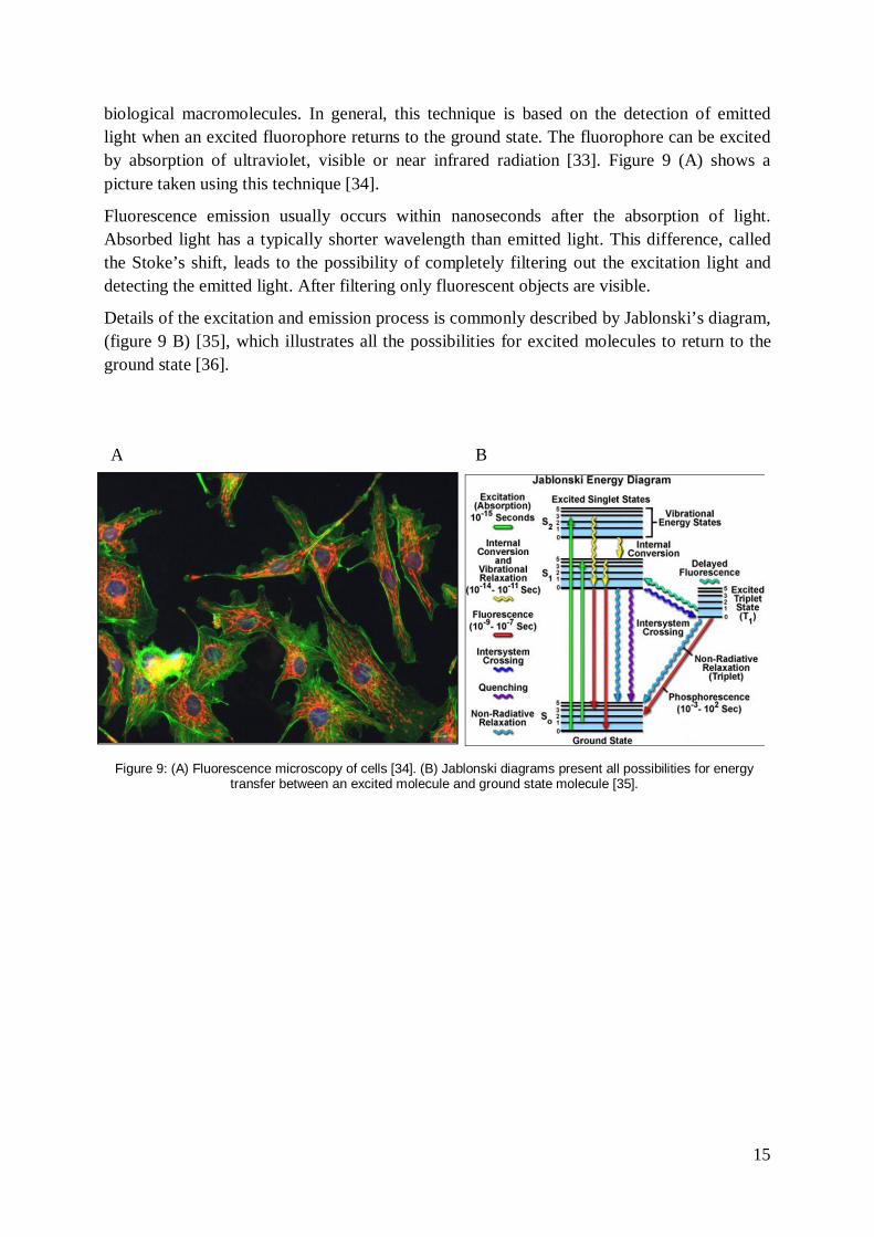
biological macromolecules. In general, this technique is based on the detection of emitted light when an excited fluorophore returns to the ground state. The fluorophore can be excited by absorption of ultraviolet, visible or near infrared radiation [33]. Figure 9 (A) shows a picture taken using this technique [34].
Fluorescence emission usually occurs within nanoseconds after the absorption of light. Absorbed light has a typically shorter wavelength than emitted light. This difference, called the Stoke’s shift, leads to the possibility of completely filtering out the excitation light and detecting the emitted light. After filtering only fluorescent objects are visible.
Details of the excitation and emission process is commonly described by Jablonski’s diagram, (figure 9 B) [35], which illustrates all the possibilities for excited molecules to return to the ground state [36].
Figure 9: (A) Fluorescence microscopy of cells [34]. (B) Jablonski diagrams present all possibilities for energy
transfer between an excited molecule and ground state molecule [35].
A B
16
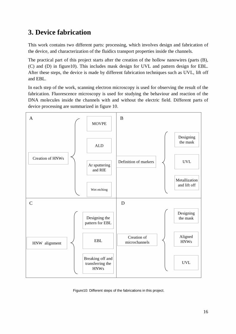
3. Device fabrication This work contains two different parts: processing, which involves design and fabrication of the device, and characterization of the fluidics transport properties inside the channels.
The practical part of this project starts after the creation of the hollow nanowires (parts (B), (C) and (D) in figure10). This includes mask design for UVL and pattern design for EBL. After these steps, the device is made by different fabrication techniques such as UVL, lift off and EBL.
In each step of the work, scanning electron microscopy is used for observing the result of the fabrication. Fluorescence microscopy is used for studying the behaviour and reaction of the DNA molecules inside the channels with and without the electric field. Different parts of device processing are summarized in figure 10.
A
C D
B
Creation of HNWs
MOVPE
ALD
Ar sputtering and RIE
Wet etching
Definition of markers UVL
Designing the mask
Metallization and lift off
Creation of microchannels
Designing the mask
Aligned HNWs
UVL
Figure10: Different steps of the fabrications in this project.
HNW alignment
Designing the pattern for EBL
EBL
Breaking off and transferring the
HNWs

17
3.1 Processing
When processing the device, different parts like, alignment of HNWs, creation of the microchannels and connecting these through HNWs, are done in a clean room (Lund Nano Lab) and the other steps like, sealing, making fluidics experiments in the microchannels and injection of DNA molecules into the device, are done in a PDMS lab and a microfluidics lab.
The work on our NWs
The hollow nanowires that are used in this project can be considered as cylindrical shells of aluminium oxide (Al2O3) that are created in four steps. NW growth, covering the NWs with aluminium oxide, breaking the tips of NWs to access to the core and wet etching for removing the core and converting the NWs to the hollow nanowires (part A in figure 10). After growing GaP nanowires to the desired length, the nanowires are covered by an aluminium oxide layer with the atomic layer deposition (ALD) technique. In the next step, the sample is covered by a resist layer. In this work, S1818 was spun on the sample and the tips of the nanowires that are sticking out of the resist were removed using argon sputtering. Any debris that redeposits on the resist is removed from the surface using oxygen plasma etching. The last step in the creation of the HNWs is selective wet etching of the GaP core, which is accessible after removing the tips. The result of the process is퐴푙 푂 tubes. The required time for wet etching the nanowires is about 5 minutes (this depends on the nanowire length). In this experiment, wet etching is done at room temperature and without agitation. For etching GaP, HCl (37%): 퐻푁푂 (65%) (3:1) is used as etching solution. These steps are summarized schematically in figure (11).
After creating the HNWs they need to be broken off from the growth substrate and transferred to the desired location with correct alignment on the main substrate. Sonication in de-ionized water is used for breaking off HNWs; after this they are suspended in the di-water. Figure 12 shows a schematic of the suspended HNWs in di-water and a 3D model of a HNW.
Figure 11: Schematic images for different steps of HNWs creation (A) NWs are covered by uniform layer of Al2O3 using ALD, (B) the resist is spun on the substrate and the tips of
NWs are broken by Ar sputtering, (C) after plasma etching the resist, HNWs are created using wet etching.
A B C

18
Figure 12: (A) Schematic image of suspended HNWs in water, (B) a 3D model of a HNW. For alignment, the HNWs are localized in desired positions defined by wells on the resist over the substrate. EBL is used for transferring the pattern of the wells to the resist-coated substrate. The required size of these wells depends on the size of HNWs and in this experiment they are 400 nm wide, 6µm length and 250nm depth. The HNWs are transferred to the main substrate in a water droplet and are randomly distributed on the surface after the water has dried (figure 13).
Figure 13: (A) Wells are created by EBL on resist-coated substrate for aligning HNWs, (B) randomly distributed
HNWs after drying the water Randomly distributed HNWs are pushed into the trenches by brushing them with a normal painting brush. They stick to the substrate and remain aligned after removing the resist. The HNWs that are not in the wells are removed by dissolving the resist (part (C) in figure 10). Details of these steps can be found in figure (14).
A B

19
Figure 14: (A) Brushing HNWs to the trenches, (B) just aligned HNWs are left after dissolving the resist. The final step of the fabrication is presented in figure (15). Microchannels are created in the photoresist on top of the aligned HNWs (part (D) in figure 10), which are lying on the substrate, and the device is sealed by a transparent polydimethylsiloxane (PDMS) sheet.
Figure 15: Schematic picture for creation of two parallel microchannels on top of the HNWs (A) before UVL and (B ) after UVL
Access to the channels is possible through holes punched through the PDMS sheet. Note that these pictures are not to scale. A cross section of the HNWs underneath the wall and the final device are shown in figure (16).

20
Figure 16: (A) Schematic picture of final device, (B) cross section of the wall on top of HNWs.
The micro and nano fabrication part of this project was considered for many different substrates such as silicon wafers and glass substrate. In our case, after testing on silicon and glass substrate and because of microscopy problems, the glass samples were preferred since flow through microchannels, and HNWs can then be seen from both sides of the samples.
The glass substrates, which were used, had a 1mm thickness and were sliced in 26x26 mm2 squares with a diamond tip cutter. After cleaning with acetone, isopropanol alcohol (IPA) and piranha cleaner (sulphuric acid 퐻 푆푂 and hydrogen peroxide 퐻 푂 (3:1)) they are ready for fabrication.
Definition of alignment marks with UVL and metallization
Since this project involves different processing stages, it was necessary to define a form of reference that can be used in all steps (part (B) in figure 10). In this way, a mask was designed (figure 17) with the software L-EDIT (The layer editor, 1988-2004, Tanner EDA, A division of Tanner research) for UV lithography.
Figure 17: Mask design for alignment markers. The red areas will be exposed on the positive
photoresist. (magnified)

21
The cleaned glass substrate was covered by the light sensitive positive resist S1813 and then the sample was exposed for 10 seconds using a mask aligner MJB4 (Suss MicroTec). After development by MF319, the sample was metalized in an evaporation system. In this way, 2-3 nm Cr was deposited for better adhesion and then 40-50 nm Au was deposited on top of the Cr. Lift off with remover 1165 and acetone was the next step for transferring the pattern and defining the origin. After lift off, the metal on the part of the substrate that was covered by resist is gone; the alignment crosses appear on the substrate. The bottom left cross (marked with a triangle) is used as the origin in next steps.
Breaking and transferring the HNWs
In the next step, the HNWs must be transferred from the growth substrate to another substrate. This can be done in different ways. Mechanical contact between the growth substrate and the new substrate and then rubbing these together is reported as a way of breaking off the NWs [37], but it seems that this method can damage the final surface, especially if there are other structures on the new substrate. For this reason, in this work the HNWs are broken by sonication in di-water. Sonication in IPA was also tested but because of the solubility of contaminants in IPA (carbon tape sticks to the back of sample during SEM inspections) water was chosen as the final liquid. Later, one droplet of this liquid is used for transferring the HNWs to the device substrate. The HNWs that are transferred in this way are randomly distributed on the surface.
Microchannels can be created on top of the randomly distributed HNWs and can be randomly connected through HNWs. In this way, there is no control of the position and direction of HNWs and, in consequence, no control of the way the two microchannels are connected to each other.
Alignment of HNWs allows the possibility of determining the position and angle of connection for the two microchannels, which can be important in measurements of the required time for the entrance of DNA into the HNWs. For this purpose, the HNWs are aligned using a combination of electron beam lithography and mechanical forces. The details of this part are explained in next section.
Alignment of the HNWs
Alignment of nanowires using electric and magnetic fields [38],[39] for metallic or multicomponent nanowires has already been done. Alignment of Au nanowires with capillary force and mechanical force has also been reported [40]. In this work, alignment of the hollow nanowires with mechanical force is chosen because of the HNWs material characteristics – these are not magnetic – and with relatively high yield for single nanowires alignment at a desired position. For this purpose, an EBL pattern of aligned wells, as described by Jong Kuk Lim et al. [40], was designed using the RAITH 150 software (Raith 150, Raith GmbH, Dortmund Germany) as shown in figure (18) below. To accommodate the size of our HNWs (3-5 µm length and 50-200 nm diameters) final wells should be around 6 µm length and 400
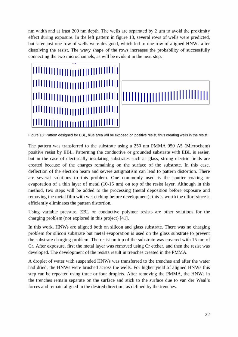
22
nm width and at least 200 nm depth. The wells are separated by 2 µm to avoid the proximity effect during exposure. In the left pattern in figure 18, several rows of wells were predicted, but later just one row of wells were designed, which led to one row of aligned HNWs after dissolving the resist. The wavy shape of the rows increases the probability of successfully connecting the two microchannels, as will be evident in the next step.
Figure 18: Pattern designed for EBL, blue area will be exposed on positive resist, thus creating wells in the resist. The pattern was transferred to the substrate using a 250 nm PMMA 950 A5 (Microchem) positive resist by EBL. Patterning the conductive or grounded substrate with EBL is easier, but in the case of electrically insulating substrates such as glass, strong electric fields are created because of the charges remaining on the surface of the substrate. In this case, deflection of the electron beam and severe astigmatism can lead to pattern distortion. There are several solutions to this problem. One commonly used is the sputter coating or evaporation of a thin layer of metal (10-15 nm) on top of the resist layer. Although in this method, two steps will be added to the processing (metal deposition before exposure and removing the metal film with wet etching before development); this is worth the effort since it efficiently eliminates the pattern distortion.
Using variable pressure, EBL or conductive polymer resists are other solutions for the charging problem (not explored in this project) [41].
In this work, HNWs are aligned both on silicon and glass substrate. There was no charging problem for silicon substrate but metal evaporation is used on the glass substrate to prevent the substrate charging problem. The resist on top of the substrate was covered with 15 nm of Cr. After exposure, first the metal layer was removed using Cr etcher, and then the resist was developed. The development of the resists result in trenches created in the PMMA.
A droplet of water with suspended HNWs was transferred to the trenches and after the water had dried, the HNWs were brushed across the wells. For higher yield of aligned HNWs this step can be repeated using three or four droplets. After removing the PMMA, the HNWs in the trenches remain separate on the surface and stick to the surface due to van der Waal’s forces and remain aligned in the desired direction, as defined by the trenches.

23
UVL on SU8
After transferring and aligning the HNWs, the next step of the processing is the creation of microchannels so that connection between them is only possible through the HNWs. For this, a mask for UVL was designed (figure 19) using the software L-EDIT and the pattern was transferred to the substrate with aligned HNWs covered by a 2 µm layer of the negative photoresist SU8 (Microchem). The triangular shapes are used as guides to the eye when doing the alignment.
Figure 19: Different masks for the creation of the microchannel. The red area will be exposed on negative photoresist. (A) Microchannels with smoother edges and four channels in parallel, (B) smoother edge for two microchannels and (C)
microchannels with sharp edges (magnified).
In this part, SU8 was chosen because of its high contrast, excellent resolution, and high sensitivity to UV sources, stability and also for the possibility of permanent application as part of the final structure of the devices [42]. SU8 has shown in practice to be very sensitive to any change in process parameters. In this work, the adhesion of the resist and substrate was strongly related to the exposure dose and post exposure baking.
SU8-2002 was prepared by dilution of SU8-2005 that already existed in the Lund nano lab by SU8 thinner (1:0.64). After exposure, post exposure baking, development by SU8 developer and hard baking, two 50 µm wide parallel channels separated by a 2µm wide SU8 wall were created on the substrate.
There was some problem with the sharp edges of the pattern (figure 19 C) in the experiments. In practice, either the sharp edges of the wall were broken in many devices or the wall was not uniform in this region. This problem was overcome by designing a new mask with smoother edges (figure 19 A and B).
In both EBL and UVL, the crosses from the first UVL step were used for the alignment.

24
Sealing the devices
Sealing the device was the final step of the fabrication and was very important for the result. SU8 coated glass before and after baking was tested as a lid but the sealing was not completely successful.
Applying pressure for binding the glass as a lid to the device was also tested. Under pressure, the device and cover glass were heated above the SU8 glass transition temperature (180˚C) for an hour. During this process non-cross linked chains diffuse to the SU8-glass interface and then cross linking occurs that leads to better adhesion between glass and polymer [43]. This technique did not work in this experiment, maybe because of the small thickness of the SU8 in the structure and lack of non-cross linked resist or lack of sufficient pressure on the device.
In the end, the device was sealed by a sheet of O2 plasma treated PDMS. The access to the microchannels was made possible through holes, which were punched in the PDMS sheet.
3.2 Characterization
A solution of Tris borate sodium EDTA (TBE) 0.5x, polyvinylpyrrolidone (PVP) 4% and 훽-mercaptoethanol (BME) 3% is used as buffer and for wetting the microchannels. PVP is added to the buffer to prevent electroosmosis and BME prevents the DNA from being broken because of the illumination [44]. To test whether or not two microchannels are connected through HNWs and whether fluidics is developed through HNWs, lambda phage DNA (휆 − 퐷푁퐴(48 kbp)) with a concentration of (10 µg/ml) is added to the buffer solution and injected into the device. DNA molecules are labelled with YOYO-1 with a concentration of 50µM (1 dye molecules per 10 base pairs).
To study transport phenomena in HNWs, passing DNA molecules through them and going from one channel to the other is a good start. At equilibrium conditions, DNA molecules are in their natural coil configuration and the small diameter of the HNWs prevents the transit of the coiled molecules. An external force is needed to push the DNA molecules through the HNWs. The negatively charged DNA molecules change their configuration to stretched molecules because of confinement [45].

25
4. Results
In this chapter, the result of the different steps of fabrication and characterization of the device for this project are presented. This chapter is divided into two different sections according to the different parts of the project. First, the result of fabrication part is presented and then results of the device characterization.
4.1 Creation of hollow nanowires
In order to create the microchannels on top of the HNWs, first of all, it was checked whether or not the nanowires are hollow after wet etching. SEM images (figure 20) from the samples show clearly that aluminium oxide shells with the inner diameter 10-80 nm and outer diameter 50-200 nm and 3-5 µm length are created successfully.
Figure 20: SEM images of HNWs after wet etching tilt 30°. The inset picture shows the etched core of the
HNWs. In figure 20, the dark area on top of the HNWs (inset) shows that the etched core. Note that its diameter varies due to the size variation of the aerosol gold particles.

26
4.2 Alignment of hollow nanowires
In the case of alignment of HNWs, rows of wells are created in PMMA using EBL. Figure 21 shows the wells on glass samples, which are covered by a 10 nm layer of sputtered palladium to prevent sample charging and to increase the possibility of obtaining a better SEM image. The left image shows the pattern of the wells when we were exploring the alignment of the HNWs and the right image shows the final pattern when it was possible to place HNWs exactly on the desired locations.
Figure 21: SEM images of trenches created in PMMA after development resist and deposition palladium.
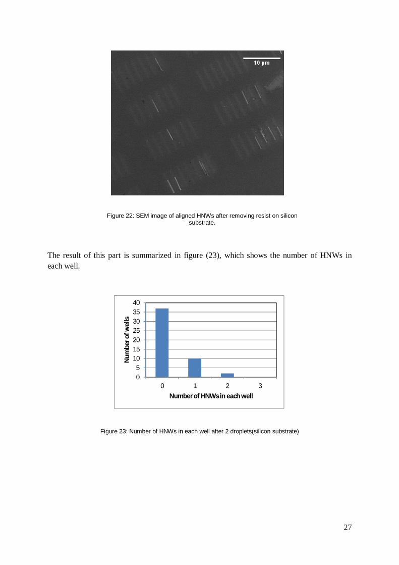
SEM images after removing the PMMA show that transferring and aligning the HNWs from the growth substrate to the final substrate in the desired direction is done successfully. According to the results, HNWs are aligned individually. In one example for the silicon substrate, after transferring two droplets, 12 of 49 wells (24%) are filled by HNWs (figure 22) of which 10 wells (20% of the all wells) contain only one HNW.
27
Figure 22: SEM image of aligned HNWs after removing resist on silicon substrate.
The result of this part is summarized in figure (23), which shows the number of HNWs in each well.
Figure 23: Number of HNWs in each well after 2 droplets(silicon substrate)
05
10152025303540
0 1 2 3
Num
ber o
f wel
ls
Number of HNWs in each well
28
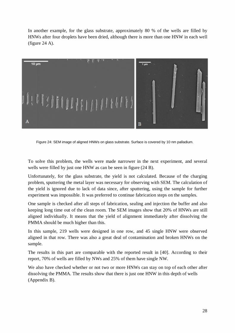
In another example, for the glass substrate, approximately 80 % of the wells are filled by HNWs after four droplets have been dried, although there is more than one HNW in each well (figure 24 A).
Figure 24: SEM image of aligned HNWs on glass substrate. Surface is covered by 10 nm palladium.
To solve this problem, the wells were made narrower in the next experiment, and several wells were filled by just one HNW as can be seen in figure (24 B).
Unfortunately, for the glass substrate, the yield is not calculated. Because of the charging problem, sputtering the metal layer was necessary for observing with SEM. The calculation of the yield is ignored due to lack of data since, after sputtering, using the sample for further experiment was impossible. It was preferred to continue fabrication steps on the samples.
One sample is checked after all steps of fabrication, sealing and injection the buffer and also keeping long time out of the clean room. The SEM images show that 20% of HNWs are still aligned individually. It means that the yield of alignment immediately after dissolving the PMMA should be much higher than this.
In this sample, 219 wells were designed in one row, and 45 single HNW were observed aligned in that row. There was also a great deal of contamination and broken HNWs on the sample.
The results in this part are comparable with the reported result in [40]. According to their report, 70% of wells are filled by NWs and 25% of them have single NW.
We also have checked whether or not two or more HNWs can stay on top of each other after dissolving the PMMA. The results show that there is just one HNW in this depth of wells (Appendix B).

29
4.3 Creation of microchannels separated by a wall on top of the HNWs
SEM images show that microchannels are created successfully, and they are separated by the wall that is exactly on top of the HNWs. The channels are connected to each other through the HNWs. SEM images clearly show that two ends of HNWs sticking out of the 2µm wide wall and appear to remain hollow after developing SU8 (figure 25 D).
4.4 Focused ion beam
To check whether or not the HNWs are blocked during the fabrication process by SU8 or other material, focused ion beam milling has been used. The SU8 wall on top of the HNWs is milled by Ga+ ions and was removed. The contrast in SEM images suggests that HNWs remain hollow and unblocked after the different fabrication steps (figure 26).
Figure 25: (A) SEM image for overview of the device showing the channels,(b) shows wall on top of the successfully aligned HNWs, (C) SEM image of both sides of aligned HNWs out of the wall
(D)SEM image of ends of HNWs not covered by SU8 photoresist.
30
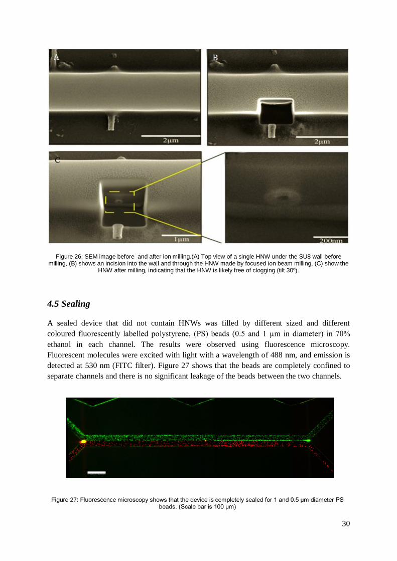
Figure 26: SEM image before and after ion milling.(A) Top view of a single HNW under the SU8 wall before milling, (B) shows an incision into the wall and through the HNW made by focused ion beam milling, (C) show the
HNW after milling, indicating that the HNW is likely free of clogging (tilt 30º).
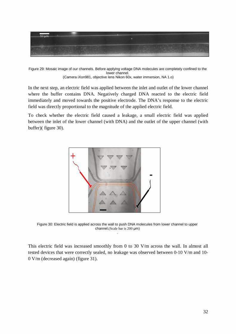
4.5 Sealing
A sealed device that did not contain HNWs was filled by different sized and different coloured fluorescently labelled polystyrene, (PS) beads (0.5 and 1 µm in diameter) in 70% ethanol in each channel. The results were observed using fluorescence microscopy. Fluorescent molecules were excited with light with a wavelength of 488 nm, and emission is detected at 530 nm (FITC filter). Figure 27 shows that the beads are completely confined to separate channels and there is no significant leakage of the beads between the two channels.
Figure 27: Fluorescence microscopy shows that the device is completely sealed for 1 and 0.5 µm diameter PS beads. (Scale bar is 100 µm)

31
4.6 DNA injection
The diameter of DNA (2nm) is much smaller than the tested beads and for guiding them through HNWs from one microchannel to the other, it is necessary to have a device with no connection other than to the HNWs. In such a device an applied external force can push the DNA molecules through the HNWs.
To test whether or not DNA can leak from one channel to the other, several devices without HNWs were tested.
First of all, 3 µl buffer ((0.5x TBE), (PVP) 4% and (BME) 3%) was added to one channel of the device. The channel was filled with buffer using capillary forces. The other channel was filled with 3 µl stained DNA and the same buffer. The filling of the channels is shown in figure (28). The injection of buffer in each channel is considered as t=0.
igure 28: Wetting the channels. Artificial red colour shows how buffer flows inside the channels.(Scale bar is 200 µm) To show that the DNA does not escape across the barrier, once the channel was filled, we tried to keep the DNA molecules in a region where the two channels are separated by the 2 µm wide wall. In order to achieve this, 3 µl of buffer was added to the outlet of the DNA channel. The DNA molecules were limited to the desired area, and no connection was observed between the two channels. This shows that the 2 µm wide wall prevents DNAs diffusion to the other channel, see figure (29).
32
Figure 29: Mosaic image of our channels. Before applying voltage DNA molecules are completely confined to the lower channel.
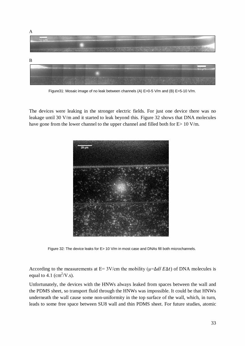
(Camera iXon981, objective lens Nikon 60x, water immersion, NA 1.o) In the next step, an electric field was applied between the inlet and outlet of the lower channel where the buffer contains DNA. Negatively charged DNA reacted to the electric field immediately and moved towards the positive electrode. The DNA’s response to the electric field was directly proportional to the magnitude of the applied electric field.
To check whether the electric field caused a leakage, a small electric field was applied between the inlet of the lower channel (with DNA) and the outlet of the upper channel (with buffer)( figure 30).
Figure 30: Electric field is applied across the wall to push DNA molecules from lower channel to upper channel.(Scale bar is 200 µm)
.
This electric field was increased smoothly from 0 to 30 V/m across the wall. In almost all tested devices that were correctly sealed, no leakage was observed between 0-10 V/m and 10-0 V/m (decreased again) (figure 31).
33
A
B
Figure31: Mosaic image of no leak between channels (A) E=0-5 V/m and (B) E=5-10 V/m.
The devices were leaking in the stronger electric fields. For just one device there was no leakage until 30 V/m and it started to leak beyond this. Figure 32 shows that DNA molecules have gone from the lower channel to the upper channel and filled both for E> 10 V/m.
Figure 32: The device leaks for E> 10 V/m in most case and DNAs fill both microchannels.
According to the measurements at E= 3V/cm the mobility (µ=∆푑/퐸∆푡) of DNA molecules is equal to 4.1 (cm2/V.s).
Unfortunately, the devices with the HNWs always leaked from spaces between the wall and the PDMS sheet, so transport fluid through the HNWs was impossible. It could be that HNWs underneath the wall cause some non-uniformity in the top surface of the wall, which, in turn, leads to some free space between SU8 wall and thin PDMS sheet. For future studies, atomic

34
force microscopy (AFM) is a powerful tool for characterizing the uniformity of the top surface of the wall.

35
5. Technical summary The thickness of the glass substrate plays an important role for determining the correct dose and exposure times for UVL. According to the resist (SU8) data sheet [42], the required dose for a glass substrate is around 1.5 times of silicon’s dose. The required energy for patterning a 2 µm tick resist on the silicon substrate is 60-80 mJ/cm2 (figure 33) and the power of mask aligner in the Lund nano lab (MJB4 Suss MicroTec) is 20mW/ cm2. It means that the required time for a silicon substrate is 3-4s and for a glass substrate, it should be 4.5-6 s, but in practice in this work, the required exposure time turned out to be around 10 times greater.
For the thick glass, the exposure time started at 6 s but the pattern was not transferred during this short time period. The exposure time increased to 20-30 s. Even during this range, transferring the pattern to the substrate was not successful. At 40-60 s the sample was sometime underexposed, and the wall was either not uniform or broken in some regions. Finally, the best result and the most uniform wall were obtained at 70 s exposure. Some of the tested samples for different exposure time are shown in figure (34).
Figure 33: Tables for dose calculation in different thickness and different substrate(35)
36
Figure 34: Under exposure sample (A) t=35s and (B) t=45s, (C) the wall is not completely formed in right edge
of the channels t=55s.
In general SU8 has shown practically to be very sensitive to any variation in the process parameters.
The resolution of the mask aligner is one of the main constraints in pattern designing. As an example in the last step of this project, the narrower wall could be aligned with even shorter HNWs. Due to resolution limitation, it was not easy to have features smaller than 2 µm with UVL.
The length of the channels in the region where they are separated by the 2µm wall is another important factor. Shorter length decreases the possibility of a wall breaking in the last step. In this experiment, this length was 2 mm in the first mask. In the second mask, we decreased the length from 2 mm to 1-1.3 mm (different channels) and in the future device, this may be decrease further.
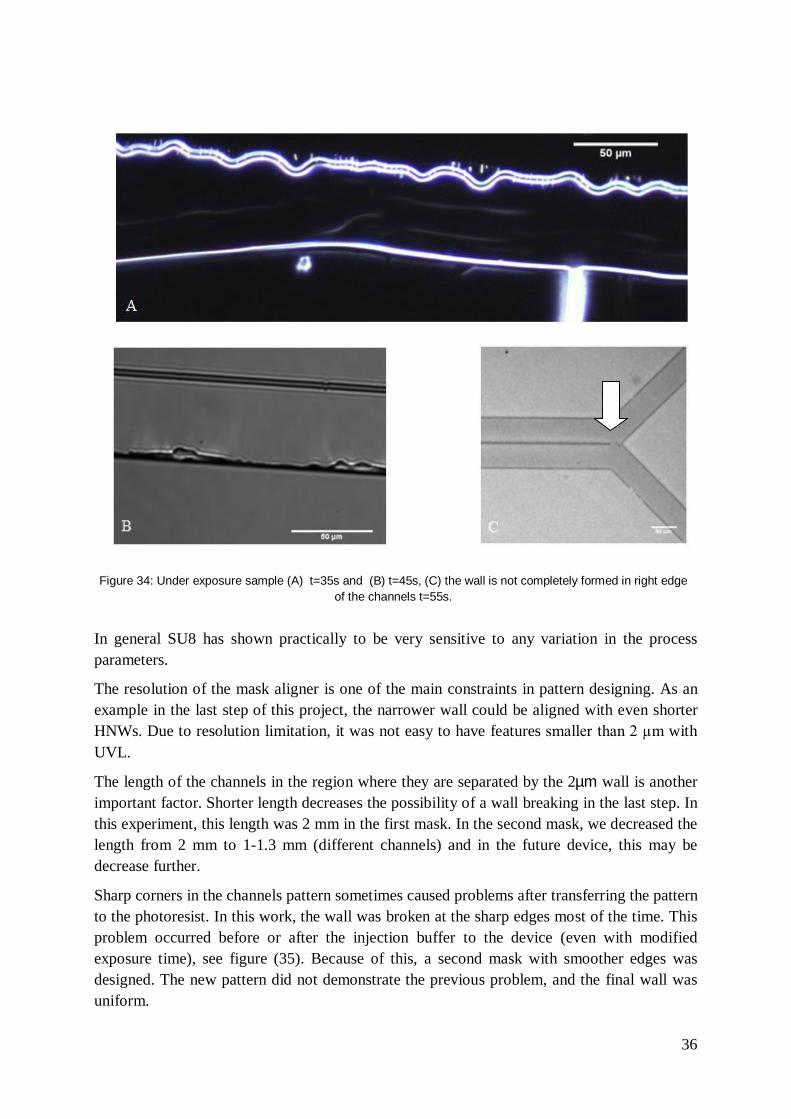
Sharp corners in the channels pattern sometimes caused problems after transferring the pattern to the photoresist. In this work, the wall was broken at the sharp edges most of the time. This problem occurred before or after the injection buffer to the device (even with modified exposure time), see figure (35). Because of this, a second mask with smoother edges was designed. The new pattern did not demonstrate the previous problem, and the final wall was uniform.

37
Figure 35: Broken sharp edge after injection DNAs.
DNA molecules were stuck to the PDMS in the inlets of the channels that were covered by a non-plasma treated PDMS sheet (figure 36) due to hydrophobic interaction [46]. This problem was solved by using O2 plasma treated PDMS. Plasma treatment of the PDMS caused the surface to be negatively charged and also more hydrophilic. Because of the repulsive force between negatively charged DNA molecules and the PDMS sheet, the molecules can move more easily inside the microchannel without sticking.
Figure 36: DNA sticks to untreated PDMS sheet.
As mentioned before, sealing is a crucial part of this work. A low pressure on top of the PDMS sheet can clog the microchannels since they are just 2 휇푚 deep. Figure (37) shows a channel being blocked by pressure applied with a finger pressure.

38
Figure 37: Channel clogged by low pressure. ( scale bars are 200 µm)
Finally for voltages greater than critical voltage (around 10 V for this device), DNA could pass through space between the SU8 wall and the PDMS sheet (figure 38). It seems that with better sealing, higher voltages can be applied, and consequently, the DNA molecules experience a greater force and enter the HNWs.
Figure 38: Time series of DNA passing over the wall between two channels. (Scale bar is 50 µm)

39
6. Conclusion and outlook
We successfully aligned HNWs one by one with respect to orientation and location with sub-µm precision. These aligned HNWs are used for connecting two parallel microchannels. Although we developed fluidics through microchannels, using the device for guidance of DNA through HNWs was not achieved and this will be the next step.
The main problem was leakage between the two microchannels. It must be overcome if the device is to be used for guidance of DNA. We observed that when HNWs are underneath of the wall (diameter of HNWs is almost 1/10 of the wall’s depth) DNA molecules always can find some spaces between the cover sheet and top surface of the wall to pass through.
Atomic force microscopy is one way of checking the uniformity of the SU8 wall. In case of non-uniformity, which leads to incomplete bonding of PDMS and SU8 wall, other methods should be tested for sealing. There are some other methods for better bonding the PDMS sheet to the SU8 wall such as covering the SU8 surface with a thin layer of material with better adhesion to the PDMS. The other alternative is to seal the device under pressure and at high temperature with another glass, which is covered by SU8. A supplementary systematic study of various processes would present all possibilities and limitations.
For this project, more than 100 samples (silicon, thin glass (100 µm) and thick glass (1mm) substrate) were prepared and tested in different steps.
Silicon wafers were easier for all steps. In case of silicon substrate, there was no charging problem both for observing with SEM and doing EBL. There was no need of sputtering metal on the sample and the sample could be tested with SEM after each step. The only problem was that silicon is non-transparent. In Bio-PL lab, the pictures must be taken from the bottom surface of the samples. Transparent substrates are more suitable. Otherwise, after each injection, the sample needs to be turned upside down to make it possible to look at the channels through the PDMS sheet.
Cleaning the glass with Piranha cleaner leads to better adhesion of the resist to the substrate.
The shape of the substrate is also important. It has to be matched by an available sample holder for each machine. In this project maybe 1-2 inches circular glass substrate would be better according to available sample holders. With a circular substrate, the vacuum contact in the mask aligner that gives the best resolution is possible. With the square samples the chuck was not able to hold the sample firmly which influenced on vacuum contact and consequently on the final resolution. It was preferable to cut the samples from available glass slides in the lab because of price, and the huge number of samples needed.
Contamination was another problem during the sealing the device in the PDMS lab. When there were dust particles on top of the wall, leakage was always observed.
In conclusion we hope this device opens up new windows for developing and studying fluidics through horizontal HNWs on different substrates and transferring macromolecules to the desired location. Measurement of the resistance of the HNWs and the required time for

40
entrance the DNA molecules to the HNWs for different voltages can be a good start to characterize the device for investigation of transport with gate.

41
Bibliography 1. Nguyen, N.-T. and S.T. Wereley, Fundamentals and Applications of Microfluidics.
second ed2006. 2. Whitesides, G.M., The origins and the future of microfluidics. Nature 2006. 442: p. 368-
373. 3. Bhupinder Singh Sekhon, S.K., Microfluidic technology for drug discovery and
development, International Journal of PharmTech Research,2010. 2: p. 804-809. 4. Eijkel, J.C.T. and A.v.d. Berg, Nanofluidics: what is it and what can we expect from it?
Microfluidic Nanofluidic, 2005. 1: p. 249-267. 5. Napoli, M., J.C.T. Eijkel, and S. Pennathur, Nanofluidic technology for biomolecule
applications: a critical review. Lab on a Chip, 2010. 10(8): p. 957-985. 6. Emmanuel G Guignet , T.M., Suspended-drop electroporation for high-throughput
delivery of biomolecules into cells. Nature Methods, 2008. 5: p. 393 - 395. 7. Jooss, K. and N. Chirmule, Immunity to adenovirus and adeno-associated viral vectors:
implications for gene therapy. Gene Ther, 0000. 10(11): p. 955-963. 8. Thompson, W.S. and R.H. Gross, Antibodies introduced into living cells with liposomes
localize specifically and inhibit specific intracellular processes. Gene Analysis Techniques, 1988. 5: p. 73-79.
9. Maxine A. McClain, C.T.C., Stephen C. Jacobson, Nancy L. Allbritton, Christopher E. Sims, J. Michael Ramsey, Microfluidic Devices for the High-Throughput Chemical Analysis of Cells. Anal. Chem., 2003. 75: p. 5646–5655.
10. Yue-Hua Dou, N.B., Jing-Juan Xu, Fei Meng, Hong-Yuan Chen, Separation of proteins on surface-modified poly(dimethylsiloxane) microfluidic devices. Int. J. Biochem. Cell Biol. Electrophoresis, 2004 25: p. 3024–3031.
11. Nicolas Minc, C.F., Kevin D. Dorfman, Aurélien Bancaud, Charlie Gosse, Cécile Goubault, Jean-Louis Viovy, Quantitative Microfluidic Separation of DNA in Self-Assembled Magnetic Matrixes. Anal. Chem., 2004. 76: p. 3770–3776.
12. Beech, J.P. and J.O. Tegenfeldt, Tuneable separation in elastomeric microfluidics devices. Lab on a Chip, 2008. 8(5): p. 657-659.
13. Golden, J.P., et al., Target delivery in a microfluidic immunosensor. Biosensors and Bioelectronics, 2007. 22(11): p. 2763-2767.
14. Folch, A. and M. Toner, Microengineering of cellular interactions. Annual Review of Biomedical Engineering, 2000. 2: p. 227-+.
15. Saltzman, W.M. and W.L. Olbricht, Building drug delivery into tissue engineering design. Nat Rev Drug Discov, 2002. 1(3): p. 177-186.
16. Xing Chen , A.K., A. Zettl ,Carolyn R. Bertozzi A cell nanoinjector based on carbon nanotubes. PNAS, 2007. 104: p. 8218-8222
17. Shalek, A.K., et al., Vertical silicon nanowires as a universal platform for delivering biomolecules into living cells. Proceedings of the National Academy of Sciences, 2010.107: p.1870-1875
18. Sköld, N., et al., Nanofluidics in hollow nanowires. Nanotechnology, 2010. 21(15): p. 155301.
42
19. Persson, H., Beech, J.P. , Samuelson, L., Prinz, C.N., Tegenfeldt, J.O., Oxide Nanotube with fluidic connection for cell injections. Under review.
20. Gates BD, X.Q., Stewart M, Ryan D, Willson CG, Whitesides GM., New approaches to nanofabrication: molding, printing, and other techniques. Chem. Rev., 2005. 105 p. 1171-1196.
21. Dick, K., Epitaxial Growth and Design of Nanowires and Complex Nanostructures 2007, Lund.
22. Sköld, N., Nanowire Hetrostructures, 2008, Lund. 23. Groner, M.D., et al., Electrical characterization of thin Al2 O3 films grown by atomic
layer deposition on silicon and various metal substrates. Thin Solid Films 186–197, 2002. 413: p. 186–197.
24. RainerBehrisch, W.E., Sputtering by Particle Bombardment2007: Springer. 25. Cardinaud, C., M.-C. Peignon, and P.-Y. Tessier, Plasma etching: principles,
mechanisms, application to micro- and nano-technologies. Applied Surface Science, 2000. 164(1-4): p. 72-83.
26. Sze, S.M., Semiconductor devices, physics and technology2002. 27. Jeremy Golden, H.M., Dan Nawrocki, Jack Ross Optimization of Bi-layer Lift-Off
Resist Process in CS MANTECH 2009: Florida, USA. 28. Ampere A. Tseng, K.C., Chii D. Chen, and Kung J. Ma, Electron beam lithography in
nanoscale fabrication: recent development IEEE, 2003. 26: p. 141 - 149 29. John J Bozzola, L.D.R., Electron Microscopy 1999. 30. David Bernard Williams, C.B.C., Transmission Electron Microscopy, 2009. 31. http://fgamedia.org/faculty/rdcormia/NANO53/SEM.htm. [cited 2011 10September ]. 32. C.A.Volkert and A.M. Minor, G.E., Focused Ion Beam Microscopy and
Micromachining. MRS BULLETIN, 2007. 32: p. 389-399. 33. Pawley, J., Handbook of Biological Confocal Microscopy2006. 34. www.rp-photonics.com/flourescence-microscopy.html. [cited 2011 11 September]. 35. http://www.olympusmicro.com/primer/java/jablonski/jabintro/index.html. [cited 2011
10 September]. 36. Lichtman, J.W. and J.-A. Conchello, Fluorescence microscopy. Nat Meth, 2005. 2(12):
p. 910-919. 37. P.Beech, J. and H. Persson, Hollow Nanowire Fluidics, 2010, project report for
Advanced Processing of Nanostructures course. 38. Peter A. Smith, C.D.N., Thomas N. Jackson, Theresa S. Mayer, Benjamin R. Martin,
Jeremiah Mbindyo, Thomas E. Mallouk Electric-field assisted assembly and alignment of metallic nanowires Applied Physics Letters, 2000. 77: p. 1399-1401.
39. M. Tanase, D.M.S., A. Hultgren, L. A. Bauer, P. C. Searson, G. J. Meyer, D. H. Reich, Magnetic trapping and self-assembly of multicomponent nanowires Journal of Applied Physics, 2002. 91: p. 8549-8551.
40. Lim, J.K., et al., Alignment Strategies for the Assembly of Nanowires with Submicron Diameters. Small, 2010. 6(16): p. 1736-1740.
41. Myers, B.D. and V.P. Dravid, Variable Pressure Electron Beam Lithography (VP-eBL): A New Tool for Direct Patterning of Nanometer-Scale Features on Substrates with Low Electrical Conductivity. Nano Letters, 2006. 6(5): p. 963-968.

43
42. SU8 2000, Permanent Epoxy Negative Photoresist, MICROCHEM, Editor. 43. S. G. Serra, A.S., K. Malecki, S. E. Huq, W. Brenner, A Simple Bonding Process of SU-
8 to Glass to Seal a Microfluidic Device, in 4M Network of Excellence2007: Borovets, Bulgaria.
44. Persson, F. and J.O. Tegenfeldt, DNA in nanochannels-directly visualizing genomic information. Chemical Society Reviews, 2010. 39(3): p. 985-999.
45. Nelson, P., Biological Physics: Energy, Information, Life 2002. 46. Bensimon, D., et al., Stretching DNA with a Receding Meniscus: Experiments and
Models. Physical Review Letters, 1995. 74(23): p. 4754-4757.
44
Appendix A
HNW fabrication
Aerosol Deposition of Gold aerosol particles with a diameter of 80 nm with a surface density of 1 µm2
on (111) B GaP substrates (Girmet Ltd, Moscow, Russia)
MOVPE Growth of GaP nanowires from the gold seeds using metal organic vapour phase epitaxy (MOVPE) (Aix 200/4, Aixtron, Herzogenrath, Germany)
ALD Covering nanowires with Al2O3 by atomic layer deposition (ALD) (Savannah 100, Cambridge Nanotech Inc., Cambridge, Massachusetts, USA).
S1818 (Microchem corp. Newton Massachusetts USA) Spin with 4000 RPM for 45 s
Bake on hot plate at 115 ˚C for 90 s
Ar sputtering (Plasma lab 100 system,Oxford Instrument, Oxfordshire UK) Chamber pressure 10mTorr
Ar flow 130 sccm
RF power 100W
ICP power 1000W
Sample temperature 25 ˚C and total running time 15 min
Sputtering rate 5 푛푚/푚푖푛 on plane surface
4” Al2O3 sample carrier (acts as electrode)
Oxygen plasma cleaning (Plasma lab 100 system,Oxford Instrument, Oxfordshire UK) Chamber pressure 15mTorr
Oxygen flow 40sccm
RF power 15W
ICP power 1500W
Sample temperature 25 ˚C and total running time 20-40 min
4” Al2O3 sample carrier (acts as electrode)
Wet etching of GaP core HCL37%: 퐻푁푂 65% (3:1)
Solution aged 5 min
Etch rate 1 휇푚/푚푖푛

45
Fabrication of microfluidic connections
Cutting & cleaning the glass (microscope slides 76*26 mm, Thermo scientific, Menzel-Gläser) Diamond tip to cut 26*26 mm and 1mm thick
Sonication in acetone 15 minutes
Sonication in IPA 15 minutes
Drying the sample using nitrogen gun
Piranha cleaner 15 minutes (Sulphuric acid 퐻 푆푂 and Hydrogen peroxide 퐻 푂 (3:1))
DI water 10 minutes
The samples can be kept in di- water for almost 2-3 weeks.
Breaking the HNWs Growth substrate was sonicated in water for 10 min at highest power.
UVL for Origin definition S1813 (Microchem corp. Newton Massachusetts USA) spun on the sample at 5000 rpm for 30 s Baked 90 s at 115˚CExposed for 10 s, power of lamp= 20mW/ cm2 (MJB4 (soft UV) Suss MicroTec)
90 s in MF319 for development and then 30 s in water
Drying using nitrogen flow
Lift Off 20 min in remover 1165 at 75˚C5 min in fresh remover 1165 at room temperature
5 min in acetone at room temperature
Rinse in water and drying completely using nitrogen flow
EBL- Raith 150 (Raith 150, Raith GmbH, Dortmund Germany) PMMA 950A5 (Microchem corp. Newton Massachusetts USA) spun on the samples at 4000 rpm for 60 s Baked 15 min at 160 ˚C
Evaporate 15 nm Cr
Exposure with dose140 µAs/cm2 and Acc voltage=10 KV
45-60 s in Cr etcher (Chrome Etch 18, OSC OrganoSpezialChemie GmbH) Rinse in water
1 min IPA+MIBK (3:1) for development and then 30s in IPA
Drying using nitrogen flow

46
UVL for microchannels Bake samples 30 min at 200˚CSU8-2002 (Microchem corp. Newton Massachusetts USA)spun on the sample at 3000 rpm for 60 s
Soft bake 1min at 65 ˚CBaked 2 min at 95 ˚CExposed 70 s, power of lamp= 20mW/ cm2 (MJB4 Suss MicroTec)
Post-exposure baked 2 min at 95 ˚CDeveloped 1 min in SU8 developer and 10 s in IPA
Drying using nitrogen flow
For better adhesion the sample can be hard baked 30 min at 200 ˚C after development
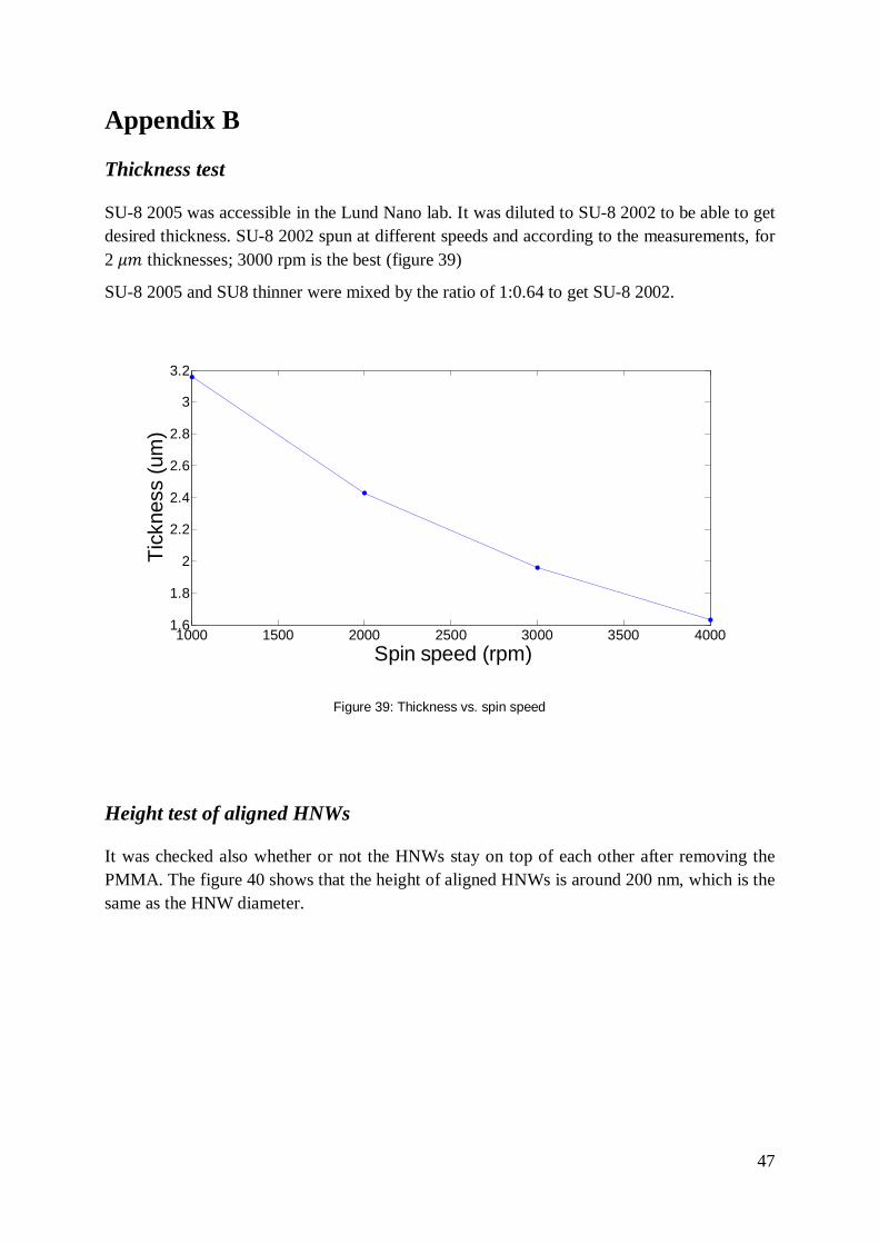
47
Appendix B
Thickness test
SU-8 2005 was accessible in the Lund Nano lab. It was diluted to SU-8 2002 to be able to get desired thickness. SU-8 2002 spun at different speeds and according to the measurements, for 2 휇푚 thicknesses; 3000 rpm is the best (figure 39)
SU-8 2005 and SU8 thinner were mixed by the ratio of 1:0.64 to get SU-8 2002.
Figure 39: Thickness vs. spin speed
Height test of aligned HNWs
It was checked also whether or not the HNWs stay on top of each other after removing the PMMA. The figure 40 shows that the height of aligned HNWs is around 200 nm, which is the same as the HNW diameter.
1000 1500 2000 2500 3000 3500 40001.6
1.8
2
2.2
2.4
2.6
2.8
3
3.2
Spin speed (rpm)
Tick
ness
(um
)
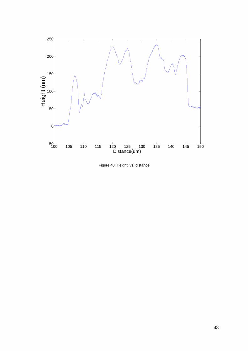
48
Figure 40: Height vs. distance
100 105 110 115 120 125 130 135 140 145 150-50
0
50
100
150
200
250
Distance(um)
Hei
ght (
nm)
49
Appendix C
Abstract and poster at Microtas 2011 (2-6 October, Seattle, USA)
MICROFLUIDIC CONNECTIONS TO HOLLOW NANOWIRES Farnaz Yadegari1,2*, Henrik Persson1,2, Mercy Lard1,2, Jason P. Beech1,2, Cassandra Niman1,2,
Lars Samuelson1,2, Heiner Linke1,2 and Jonas O. Tegenfeldt1,2,3 1 Lund University, SWEDEN
2 The Nanometer Structure Consortium at Lund University (nmC@LU), SWEDEN 3 University of Gothenburg, SWEDEN
ABSTRACT
We have fabricated a device in which hollow nanowires (HNWs) lying on a glass surface are connected to microfluidic channels for the purpose of guiding DNA and to characterize the fluidic properties of our HNWs. The dimensions of our HNWs (inner diameter 10-80 nm, outer diameter 50-200 nm and length several µm) can be made on a scale much smaller than the size of a cell and on the same order of magnitude as the Debye length, making them interesting both for applications involving direct chemical access to the cytosol of living cells and for investigations of basic transport phenomena. KEYWORDS: hollow nanowires, nanofluidics, microfluidic connections, DNA electrophoresis, flow characterization
INTRODUCTION
The small size is a unique feature of hollow nanowires (HNWs) that makes them useful for transport of molecules into and out of cells or to direct molecules to selected destinations on a chip. Due to the importance of transferring fluid through these nanoscale tubes, we have fabricated the current device to gain a deeper understanding of the fluidics in our hollow nanowires.
Large ensembles of vertical hollow nanowires have previously been shown by us to be able to transport liquids [1, 2] and vertical arrays of solid nanowires have been used by other groups to inject molecules into cells, see for instance [3]. In the current application the HNWs are horizontal and perpendicular to the optical axis to provide easier viewing of molecules inside the HNWs, observation of individual wires, and analysis of fluidic flow.
EXPERIMENTAL
The fabrication process is outlined in Figure 1. The hollow nanowires are created by covering epitaxially grown gallium phosphide nanowires (NWs) with a 50 nm aluminium oxide layer using atomic layer deposition (ALD), figure 1a. The NWs are partially embedded in a resist layer and argon sputtering is used to remove the protruding tips of these NWs to expose the semiconductor core, figure 1b. The semiconductor core is subsequently selectively etched using wet etching, figure 1c, leaving hollow oxide nanotubes as previously described [2]. The HNWs are then broken off of their substrate and suspended in water by means of sonication, figure 1d.
To align the nanowires on the substrate we have adapted a procedure previously reported by Lim et al [4]. Poly-methylmetacrylate (PMMA950 A5) is spun onto a glass substrate and subsequently covered by chromium to prevent charging during electron beam lithography (EBL). A pattern of trenches is transferred to the PMMA using EBL, figure 1f. After exposure and development the HNWs, which are suspended in water, are transferred to the substrate in a droplet. When the water evaporates the HNWs are pushed into the trenches by brushing. Even after dissolving the PMMA the HNWs remain aligned, figure 1g. SU8 is subsequently spun on top of the substrate and UV-lithography is used to expose the larger microfluidics region of the final structure, figure 1h. Using alignment markers defined by UV-lithography it is possible to precisely align the microchannels with the HNWs. The fluidic transport channels are 50 m wide and 2 mm long at the centre, the wall separating the channels is 2 m wide, and the thickness of the SU8 is 2 m throughout.
The device was sealed with a sheet of O2 plasma treated poly-dimethylsiloxane (PDMS). Holes were punched through the sheet to allow access to the channels which were then filled with, fluorescently labelled polystyrene, (PS) beads (0.5 and 1µm in diameter) in 70% ethanol and the results were observed using fluorescence microscopy. The device used for this experiment did not contain any HNWs.

50
RESULTS AND DISCUSSION Figure 2a shows a scanning electron microscopy (SEM) image of hollow nanowires after wet etching. The
EBL defined PMMA trenches are shown in Figure 2b, along with the aligned HNW after removal of the PMMA 2c, and an overview of the final device along with HNWs connecting two parallel channels defined in SU8, 2d. Figure 2e shows the results of the device filling experiments, clearly showing that PS beads cannot travel between the two parallel channels due to the narrow SU8 wall. A close-up of HNWs and their SU8 wall is shown in figure 3. In figure 3 focused ion beam (FIB) milling has been used to cut into the SU8 wall and a single HNW to investigate whether or not the HNW contained any residual resist after the UV-lithography. Figure 3 d-e) suggest that the HNWs remain hollow throughout the fabrication process.
Figure 1: Fabrication of the hollow nanowires and their microfluidic connections. a) GaP nanowires are coated with Al2O3 using ALD. b) Argon sputtering is used to remove the tips. c) Exposed GaP core is selectively etched
down to substrate using wet etching. d) Sample is submerged in water and sonicated, suspending the hollow nanowires in the water. e) An EBL defined pattern of wells is formed in PMMA resist on glass. f) A droplet of
the water containing the hollow nanowires is added to surface and after the water has evaporated the HNWs are brushed into the wells. g) PMMA is removed leaving the aligned HNWs attached to the substrate. h) UV-
lithography is used to pattern SU8 on top of HNWs.
Figure 2: a) hollow nanowires on their gallium phosphide substrate before being suspended in water. b) EBL
defined trenches in PMMA. c) arrays of HNWs aligned on the surface after removal of PMMA. d) SEM micrograph showing aligned HNWs bridging the wall separating the two channels (wires are indicated by yellow arows). e) fluorescence image showing polystyrene beads of different colours in the two parallel
channels.

51
Figure 3: SEM images showing hollow nanowires under the SU8 wall separating the two channels. a) and b)
show top views of two single HNWs and c) shows an incision into the wall and through a HNW made by focused ion beam milling. d) and e) show the exposed HNW from c), indicating that the HNW is likely free of clogging
(tilt 30). CONCLUSION
We have fabricated a device with microfluidic connections to our hollow nanowires giving us the ability to run fluidic experiments to characterize the fluid handling properties of our HNWs. To test the fluidic properties of our device we have filled the channels with fluorescent beads and to check that the HNWs are not clogged we have used FIB milling and SEM to image their interior. Based on our results with FIB milling we believe that our hollow nanowires are suitable for DNA transport as the HNWs appear to remain hollow after device fabrication is completed.
ACKNOWLEDGEMENTS
This research was funded by the Nanometer Structure Consortium at Lund University (nmC@LU), the Swedish Council for Strategic Research, the Knut and Alice Wallenberg Foundation and the Crafoord Foundation. REFERENCES [1] Sköld et al., Nanofluidics in hollow nanowires, Nanotechnology vol. 21, pp. 155301(4pp), (2010). [2] Persson et al., Arrays of Oxide Nanotubes with Integrated Microfluidic Connections, under review, (2011). [3] Shalek et al., Vertical silicon nanowires as a universal platform for delivering biomolecules into living cells,
P. Natl. Acad. Sci. USA vol. 107 pp. 1870-5, (2010). [4] Lim et al., Alignment Strategies for the Assembly of Nanowires with Submicron Diameters, Small vol. 6,
pp. 1736-1740, (2010). CONTACT
*Farnaz Yadegari, tel: +46-46-2229456, E-mail: [email protected]

52