fm modulation of a cw laser beam - nasa · fm modulation of a cw laser beam ... for angle...
TRANSCRIPT

/ J
‘NASA CONTRACTOR
REPORT
FM MODULATION OF A CW LASER BEAM
Pre)a red by
AIRCRAFT ARMAMENTS, INC.
Cockeysville, Md.
for Goddard S’ace FL@ Center
NATIONAL AERONAUTICS AND SPACE ADMINISTRATION l WASHINGTON, D. C. . FEBRUARY 1967
https://ntrs.nasa.gov/search.jsp?R=19670008029 2018-07-30T02:32:51+00:00Z

TECH LIBRARY KAFB, NM
FM MODULATION OF A CW LASER BEAM
Distribution of this report is provided in the interest of information exchange. Responsibility for the contents resides in the author or organization that prepared it.
Prepared under Contract No. NAS 5-9660 by AIRCRAFT ARMAMENTS, INC.
Cockeysville, Md.
for Goddard Space Flight Center
NATIONAL AERONAUTICS AND SPACE ADMINISTRATION
For sale by the Clearinghouse for Federal Scientific and Technical information Springfield, Virginia 22151 - Price $2.50
AESTPSICT
This report.documents the analytical and experimental studies
performed under Contract NAS5-9450. Frequency modulation and demodulation
methods for CW lasers are analyzed in terms of amplitude noise sensitivity.
Expressions are derived for detector noise limited signal to noise perfor-
mance. Results of experiments performed with homodyne, optical discrim-
inator and heterodync detection breadboards are reported. An experimental
transmitted reference heterodyne detection, angle modulated system is
described. The modulator utilizes a 45 degree Y cut ADP crystal with
length to thickness ratio of S. Performance of the experimental bread-
board over a 300 meter turbulent atmospheric path indicates that the angle
modulated transmitted reference heterodyne system is insensitive to
atmospherically induced .noise fluctuations. Improvements in laser frc-
quency stability are indicated to permit evaluation of broadband mod-
ulation capability.
ii

Table of Contents
I. Analytical Study . . . . . . . . . . . . . . . . . . . . . . . . . . . . . . . . . . . . 1
A.
B.
C.
D.
Modulation of an Optical Carrier................ 1
1. phase modulation
2. frequency modulation
3. transverse Pockels effect
Demodulation of an Optical Carrier.............. 7
1. homodyne detection
2. optical discriminator
3. heterodyne detection
Detector Noise Limited Performance.............. 18
1. DSSC modulation
2. envelope modulation
3. phase modulation - heterodyne detection
4. angle modulation - optical discriminator
Effects of Additive Noise before Detection...... 30
1. amplitude modulation
2. phase modulation
3. comparative performance
II. Experimental Study . . . . . . . . . . . . . . . . . . . . . . . . . . . . . . . . . . 35
A. 45O Y Cut ADP Modulator .*.,..................... 35
1. Electra-optic material
iii

C-
2. modulator configuration
3. modulator performance
B. Demodulator Breadboards . . . . . . . . . . . . . . . . ...45
1. homodyne
2. optical discriminator
3. heterodyne
III. Breadboard System . . . . . . . . . . . . . . . . . . . . . . . . . . . . . 56
A. Hardware Description . . . . . . . . . . . . . . . . . . . ...56
1. transmitter unit
2. receiver unit
3. modulation - demodulation electronics
B. Performance Analysis . . . . . . . . . . . . . . . . . . . ...74
1. signal considerations
2. noise considerations
C. Experimental Data . . . . . . . . . . . . . . . . . . . . . . . . 80
1. servo noise
2. subcarrier modulation
3. video modulation
iv

1.
2.
3.
4.
5.
6.
7.
8.
9.
10.
11.
12.
13.
14.
15.
16.
17.
18.
19.
20.
List of Illustrations
Transverse Pockels Effect Modulator ............................. 6
Optical Homodyne Transmitter 8 ....................................
Birefringent FM Demodulator ..................................... 11
Balanced Optical Discriminator .................................. 12
Optical Transmitted Reference Heterodyne System ................. 16
DSSC Demodulation ............................................... 19
Signal/Noise Output DSSC Demodulation ........................... 21
Signal/Noise Output Envelope Detection .......................... 22
Heterodyne Detection ............................................ 23
Signal/Noise Heterodyne Detection ............................... 24
Optical Discriminator, Frequency Modulation ..................... 25
Optical Discriminator, Phase Modulation ......................... 27
Maximum ( $)F or Selected Modulation Systems ................... 29
Electra-Optic Coefficient, r41, of Selected Class 42m Materials
at 546 nm. ..................................................... 36
Modulator Crystal Holder ........................................ 37
Graphical Analysis, Fringe Field Capacitance .................... 39
Crystal Voltage, Dissipation as a Function of Terminal Voltage..4 0
Crystal Voltage, Dissipation as a Function of Terminal Voltage..4 2
Baseband Modulator .............................................. 43
Homodyne Optical Breadboard ..................................... 46
21;.- Homodyne Detected Signal . . . . . . . . . . . . . . . . . . . . . . . . . . . . . . . . . . . . . . . . 49
V

22.
23.
24.
25.
26.
27.
28.
29.
30.
31.
32.
33.
34.
35.
36.
37.
38.
39.
Optical Discriminator Breadboard 50 ............................... .
Parameters for L/t = 4 Crystal in Optical Discriminator.........5 2
Optical Discriminator Detected Signal ........................... 53
Heterodyne Optical Breadboard ................................... 54
Transmitted Reference Heterodyne Laser Communications System....5 7
Breadboard Model . Transmitter Unit ............................. 58
Secondary Beam Collimator Ray Diagram ........................... 61
Breadboard Model - Receiver Unit ................................ 63
Receiver Optics Geometry ........................................ 64
Driver Amplifier Schematic ...................................... 68
Driver Amplifier Controls ....................................... 69
Modulation Electronics .......................................... 70
Broadband Video Modulation ...................................... 71
Mixer Pre-driver Amplifier Schematic ............................ 73
Received Signal Power as a Function of Range....................7 4
Received Signal Power for 3 Kilometer Air.......................7 6
Radiance at 0.633 Microns for Selected Sources..................7 7
Detector Noise Limited S/N as a Function of Range...............8 0
Vi

I. ANALYTICAL STUDY
A. Modulation of an Optical Carrier
An objective of this study is to investigate electro-optic methods
for angle modulation of a CW laser beam. In order to present a uniform
discussion of techniques implemented dking the contract, introductory
sections on modulation theory follow.
1. Phase Modulation
Consider a time dependent carrier signal of the form:
e(t) = Ecos(2ffct+0) (1)
Phase modulation of the signal involves variation in the phase angle, 0,
of the form:
e = - K S(t) (2)
The modulated signal is given by substituting (2) in (1):
M(t) = E cos 112 fl fc t - K S(t)] (3)
If the modulation signal, S(t), is normalized such that 1 S(t)max\ = 1;
K is the modulation index. It is numerically equal to the maximum value
of phase deviation from the unmodulated state.
The spectrum of M(t) is obtained by expanding the cosine argument and
substituting the series expansions for cos KS(t) and sin KS(t).
M(t) = E [cos (2 fi f,t) cos KS(t) -!- sin (21-t fct) sin KS(t)] (f+a)
1

Expanding:
M(t) = E cos (2 JI fct) -I- E KS(t) sin (2 TC f,t) (4b)
- E K2S2(t) E K3S3(t) 2 I
cos (2 ll fct) - 3' sin (215 f,t) .
+. . . 1
If K c 4, the spectrum is represented by the first two terms. This modu-
lation is linear. Let the modulation be of the form:
s (t) = cos (2 3x fmt) (5)
Substituting (5) in (4) for K < < 1 and expanding using the relation,
sin A cos B = l/2 (A + B) + l/2 sin (A - B),
gives:
M(t) = E cos (2 fl f,t)
+ EK 2 [sin 2 J[ (fc + fm) t] + +[sin 2 fl (fc - f,)tl (6)
The phase modulated wave for small K consists of the carrier plus upper and
lower sidebands in phase quadrature spaced 2 f apart. n Sideband amplitude
is reduced by K/2. For large values of K the spectrum becomes more complex
containing integer harmonics, fc+2f n' fc+3f m' etc.
2. Frequency Modulation
A frequency modulated wave is described by the expression:
M(t) E cos [2 x fct - 2 fi Ds S(t) dtl (7)
where S(t) is the modulating wave. If S(t) is normalized such that
2

1 SWmxl = 1, the frequency deviation, D, is numerically equal to the
maximum deviation of the instantaneous frequency from the unmodulated value,
f C’
Define quantities as follows:
In = 1 s S(t) dt 1 max
R(t) = + l S(t) dt m
K I: 21rD1 m
Cab)
(8b)
(8~)
Substitution of these quantities permits writing (7) in the form.:
M(t) = E cos c 2 5( fct - Wt)] (9)
which is identical to a phase modulated wave where K is the modulation index
and R(t) is the modulating signal. The spectrum of a frequency modulated
wave is therefore identical to that of a phase modulated wave. Consider
a modulating signal of the form
s(t) = sin 2 fl fmt
Evaluating terms,
j- S(t) dt = 1 2lTf
cos (2 7t fnt>
n
1 so that: I =
2Jrf K = D m n f m
The equivalent phase modulated wave is
M(t) = E cos [ 2 fl fct - D f,
cos (2 71 fnt)]
3
(10)
(11)

Bandwidth of the frequency modulated wave is
B = 2 fm(K+l) = 2 (D+fn) (12)
Wideband FM is defined by D > > f such that B = 2D; narrow band FM by m
D < < fm such that B = 2 fm. Note that in the second case the bandwidth
is identical to the phase modulated case where K < < 1.
The preceding discussion of phase and frequency modulation
shows that they are mathematically equivalent. In the case of modulation
of a CW laser, as studied during this contract, the modulating wave is
phase modulated on the optical carrier and demodulated by a frequency
discriminator. It is necessary therefore to compensate the system by
forming the product of the time integral of the demodulated waveform
times, 2 II D.
K R (t) = 2nDJS(t) dt (13)
In this manner, frequency modulation of the CW laser bean is achieved.
3. Transverse Pockels Effect
The method employed for modulation of the optical carrier
is the transverse Pockels effect in a suitable electro-optic crystal.
The voltage induced birefringence in a crystal of ordinary index of
refraction, n 0’
and extraordinary index of refraction, n c, is given by
b = no - n = ra,b v no3 e --
t (14)
4

where: v
t is .the applied field
ra,b is the eledtro-optic constant for
the propagation plane in the crystal
The instantaneous phase deviation between mutually orthogonal vectors of
wavelength AC, after propagating a distance L along the extraordinary
and ordinary ray axes respectively is:
A$ = p bL C
Substituting (14) for b:
h ai = F ra,b V no3 4 C
(15)
Notice that the instantaneous phase deviation is proportional to the
applied voltage and the length to thickness ratio of the crystal. The
practical advantage of transverse Pockels effect modulation is the reduc-
tion in required drive voltage for a fixed phase deviation associated
with increased modulator crystal length.
A transverse Pockels effect modulator is shown in figure 1.
Since one-half of the total retardation is attributed to each axis, i.e.
the fast axis advances the wave by @ while the slow axis retards the 2
0 wave by 2 : and since propagation is along a single axis as shown in
the figure; the expression for the modulated wave is:
M(t) = E cos p fi fct - f ra b no 3 t v cos (2 Jt fmt)IJ (17) C 9

VC3 J
--
Figure 1. TRANSVERSE POCKELS EFFECT MODULATOR

This is a phase modulated wave with:
K=f =f 'a,b no
3 L v; t R(t) = cos (2 3l fmt) (18)
m C
Complexity of the spectrum of the modulated wave, or equivalently the
maximum frequency deviation is determined by the modulation drive voltage
on the crystal. A crystal that has a large electro-optic constant and
good optical properties is desired for a transverse Pockels modulator.
B. Demodulation of an Optical Carrier
Techniques for demodulation of a frequency modulated optical
carrier studied during this contract are coherent mixing, both homodyne
and heterodyne; and optical discrimination, the birefringent demodulator'
and the balanced discriminator 2 . Objective of this study is to determine
the optimum demodulation scheme in terms of noise response. Specifically,
this means choosing a scheme that permits limiting of the modulated wave
to remove amplitude noise fluctuations while preserving the phase informa-
tion. Certain advantages of FM over AM at microwave frequencies are
derived from the limiting operation that makes the receiver insensitive
to amplitude noise fluctuations. A system that provides similar per-
formance at optical frequencies is the objective of this study. The
evaluation of demodulation methods is based upon this objective.
1. Harris, S.E., "Demodulation of Phase Modulated L,ight Using Birefringent Crystals," Proc. IEEE, Vol. 52, No.7, pp.823-831.
2. Kaminow, I.P., "Balanced Optical Discriminator", Applied Optics, Vol. 3, Nr. 4, pp.507-510.

1. Homodyne Detection
Homodyne detection is a special case of heterodyne detection
in which the local oscillator is an exact replica of the carrier. It
involves coherent mixing of the signal modulated carrier component with
an unmodulated carrier component on a suitable square law device. A
practical method for implementing honodyne detection over a duplex link
is to combine the signal carrier component and the local oscillator
component at the transmitter; e.g. as shown in figure 2. The composite
signal is transmitted to the receiver.
M I RROR
fi T&‘iNSVHTTED WAVE
Figure 2. Optical Homodyne Transmitter
In the transmitter unit the carrier signal is intensity split
into two components by an interferometer beamsplitter. One arm of the
interferometer contains a double pass modulator, the other arm delays the
local oscillator reference beam. The transmitted wave is described by

m(t) = El cos [2 x fct - KS(t)] -t E2 cos [2 fl f t - 91 C (19)
where the first term is the modulated component, the second term is the
reference. Square law detection of this signal gives:
m2(t> = El2 cos 2 [2 I-C fct - KS(t)l + E22 cos2 (2 r[ fct - 0)
(20)
+ 2 ElE2 cos [2 fi fct - KS(t)T cos (2 J[ fct - e)
The squared terms give a DC component and the second harmonic. Using the
identity cos A + cos B = 2 cos l/2 (A + B) cos l/2 (A-B) the product term
may be written:
e(t) = El E2 ~0s [4 fl fct - KS(t) - O] -I- El E2 cos [e - KS(t)]
(21)
The second harmonic and DC components are ignored in the detection process.
If the phase difference between the two waves is an odd integer number of
quarter wavelengths, i.e: 0 = nR , n = 1, 3, 5 . . . , the difference 2
term is
e'(t) = El E2 sin KS(t) (22)
For K < < 1, the modulation is recovered.
e” (t) = El E2 KS (t) (23)
It is apparent that the homodyne system is sensitive to
variations in the carrier amplitudes El and E2. Since it is a transmitted
reference scheme, atmospherically induced phase fluctuations affect both
9

components equally and are not detectable. The relative phase angle 8,
between the two wave components remains constant throughout the propaga-
tion path so the condition imposed upon it is satisfied at the detector.
Because the homodyne system is amplitude noise sensitive, it is not con-
sidered a suitable demodulation method for the purposes of this contract.
2. Optical Discriminator
There are two methods of implementing direct optical discrini-
nation of the frequency modulated optical carrier. These are the bire-
fringent demodulator and balanced discriminator referenced earlier and
shown in figures 3 and 4 respectively. Analysis of both demodulation
methods is identical. In each implementation the frequency modulated
carrier wave is split into two components with a relative time delay
inserted between them. The beams are then recombined and square law
detected.
The two signal components may be described by
t m(t) = E cos [2 JI fct - 2 II D s S(t) dt] (244
‘7 n(t-7) = E cos[2 IX fc(t -7) - 2 fl D St S(t) d t] (24b)
where T is the relative time delay. Square law detection of the two
signals yields:
[m(t) + m (t - ~>3 2 = m2(t) + m2 (t - 7) + 2m (t) m (t - 7)
(25)
10

Figure 3: BIREFRINGENT FM DEMODULATOR

-t; Eco+& -2rD S&it] O”“R i
SPLITTER h/l IRROR
Figure 4. BALANCED OPTICAL DISCRIMINATOR

Consider only the product term, that gives the sum and difference frequen-
cies. The squared terms give DC and second harmonic components that are
ignored in the detection process.
2 m(t) m(t-T) = 2 E2cos[2xfct - 2nDJtS(t) dt] cos E2nfc(t-7)-2fiD[$)dq
(26)
Using the identity, cos A cos B = l/2 cos (A+B) + l/2 cos (A-B), and
dropping the sum term, (26) may be written:
t e(t) = E2cos [2 3c fcT - 2 r[ D l S(t) dt]
t--r (27)
If 2 fl fcr = NJr; fCT = N; N = 1, 3, 5 then (27) becomes: 2 4
le’ (t-1 = E2 sin c2 x D It s(t) dtj t-7
(28)
Since the modulating wave, S(t), is of the form sin w t, the m
integral may be evaluated as follows:
t
s sin w t dt = - cos Wmt + cos (W,t - WmT)
t-T m
Wm wm (29)
Expanding cos (lu,t - w,~), collecting terns, and multiplying through by
I-., (29) becomes: 7
t
s sin wmt dt = 7 sin wmt(SiE y) - 7 COS wnt (
l- cos wrnT -1 (30)
t-T m WmT
13

Series expansion of the terms in parentheses gives:
sin wm7 2 4
=I- (wrnT > (W,T) _ . . .
wmT 3' + 5' . . Wa)
1 - cos (UlmT) (nmT brnT ) 3 = +. . . (31b)
*mT 2' 4' . .
For wrn-r < 2.8 radians, where fm = wm is the highest frequency in S(t); an 2X
approximation good to within 3 db is:
s t sin u) tdt w 7 sinw t t-T
m m (32)
Involved here is an averaging of a sine wave over an interval T. The
constraint imposed, wrn7 < 2.8, assures that the sine wave amplitude is
essentially constant over the averaging interval and therefore S(t) may
be removed from the integral.
With the above assumption equation (28) may be written:
I e’ (t> 1 %E2 sin [2fi DT S(t)] (33)
The sine wave is linear within 10% if 2 fl D T S(t) < or D T S(t) < +
or D 7 < $, since IS(t) I,, = 1. Therefore:
1 e' (t) \ Rd 2 n E2 D 7 s(t) (34)
For sinusoidal modulation, since K = 2fiD - and D T < 1 then wm 8'
wmT < &; which is more restrictive than wrn7 < 2.8 if K> 0.28.
14

Note that the detected signal is sensitive to amplitude
fluctuations of the carrier through the dependence on E2. Further, since
the detector is a frequency demodulator all frequency fluctuations appear
in the output through DS(t). The frequency fluctuations are proportional
to the time derivative of the phase fluctuations, so phase fluctuations
produce a noise output also. The system does have an amplitude noise
suppression characteristic at the modulation frequency, w,; however, this
rejection falls off rapidly at either side of wm. Comparing the optical
discriminator with homodyne detection, performance is similar if 2rr D T = K
Homodyne 1 e" (t) 1 ca El E2 K S(t) (23)
Optical discriminator Ie' (t) \ ';= 2 n E2 D I- S(t) (34)
Since K = 2 fi D , the condition for similarity of the two systems is w m
equivalently wrn7 = 1. Frequency and phase noise fluctuations do not
affect the homodyne system however. Because the optical discriminator is
amplitude noise sensitive it is not considered a suitable demodulation
method for the purposes of this contract.
3. Heterodyne Detection
A third method for demodulating a frequency modulated optical
carrier is coherent heterodyne detection. This method may be implemented
with the local oscillator signal generated either at the receiver or at
the transmitter. In the case of a locally generated reference signal at
the receiver the problem of matching phase of the two signal wavefronts
15

for good mixing action is a difficult task. Phase variation in the differ-
ence frequency signal generated at various points on the detector may cause
total loss of signal if the wavefronts are not matched. Atmospherically
induced phase distortion of the signal carrier may degrade signal perform-
ance significantly. A transmitted reference scheme for the local oscillator
signal avoids the phase matching problem since both wavefronts are distorted
by the intervening medium in an identical manner. If there is good mixing
action at the transmitter there is good mixing anywhere in the transmitted
beam.
A transmitted reference heterodyne system is shown in Figure 5.
I I
PoLARl ZEI?
BEAM H TRANSMITTED LASEF: MODULAT01’ -7 COb’iBlNER
W BEAM
Figure 5. OPTICAL TRANSMITTED REFERENCE HETERODYNE SYSTEM
16
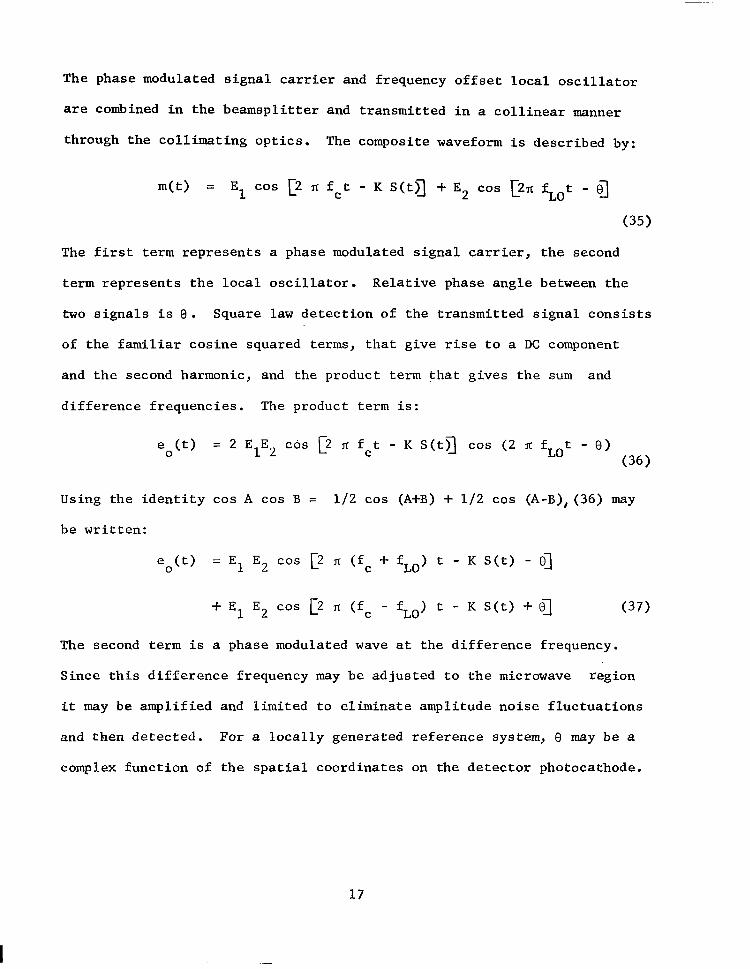
The phase modulated signal carrier and frequency offset local oscillator
are combined in the beamsplitter and transmitted in a collinear manner
through the collimating optics. The composite waveform is described by:
m(t) = El cos p 'IC fct - K S(t)lj + E2 cos p3-t f LO t - 83
(35)
The first term represents a phase modulated signal carrier, the second
term represents the local oscillator. Relative phase angle between the
two signals is 0. Square law detection of the transmitted signal consists
of the familiar cosine squared terms, that give rise to a DC component
and the second harmonic, and the product term that gives the sum and
difference frequencies. The product term is:
e,(t) = 2 ElE2 cos p JI fct - K S(tfl cos (2 x fLOt - 0) (36)
Using the identity cos A cos B = l/2 cos (A+B) + l/2 cos (A-B),(36) IMY
be written:
e,(t) = El E2 cos [2 fi (fc + fLo) t - K S(t) - @]
+ El E2 cos [2 JI (f C
- fLo) t - K S(t) + e] (37)
The second term is a phase modulated wave at the difference frequency.
Since this difference frequency may be adjusted to the microwave region
it may be amplified and limited to eliminate amplitude noise fluctuations
and then detected. For a locally generated reference system, 0 may be a
complex function of the spatial coordinates on the detector photocathode.
17

In the case of a transmitted reference system it is a constant.
The transmitted reference heterodyne detection method is not
sensitive to amplitude noise fluctuations and is unaffected by atmospheri-
cally induced phase distortion. For these reasons a transmitted reference
heterodyne system is chosen for implementation on this contract. Combined
with a transverse Pockels effect phase modulator, the transmitted reference
heterodyne detection scheme constitutes a frequency modulated optical
communications system.
C. Detector Noise Limited Performance
The desirability of implementing a transverse Pockels effect modu-
lator and transmitted reference heterodyne demodulator to obtain an FM
optical communications system is indicated in the preceding sections of
this report. It is informative to investigate the signal to noise ratio
at the output of the first demodulator, optical detector, for various
modulation schemes. The noise power density is proportional to the average
power in the signals applied to the first demodulator, which is assumed
to be a square law device.
Thus: No (f) = k Pavg (38a)
and L n,(t) = k 'avg (38b)
where P avg
is the average power at the input to the first detector and B
is the bandwidth of the demodulated wave. In the following discussion
S(t) or r(t) represents the second modulated wave; i.e., the signal to be
impressed upon the optical carrier.
18

1. DSSC Modulation
In double side band suppressed carrier modulation the modulated
wave may be expressed by
m(t) = s(t) cos 2 Jr fct (39)
In order to demodulate this wave in a square law detector, a replica of
the carrier, E cos 2 n fct, must be added as shown in Figure 6.
Figure 6. DSSC DEMODULATION
Output of the square law device is
el (t> = [m(t) f E cos 2 IX fcq2
= [E + S(ta2 cos2 2 n fct
by substitution of (39). Expansion of the expression in brackets and
use of the identity cos2 A = l/2 + l/2 cos 2A gives:
e,(t) = p2 + 2 E S(t) + S2(t)7 + [ 1 + cos 2 n (2 f,>q
(41)
19

The output is composed of some low frequency terms, p2 + 2 ES(t) + S2(tjl,
and some amplitude modulation of a carrier of frequency 2 fcF Only the
low frequency terms are passed by the bandpass filter shown in Figure 6.
In addition if S(t) has a bandwidth less than an octave; i.e. fH 2 2 fL,
where f H is the highest frequency in S(t) and fL is the lowest; and since
S2(t) has a D.C. term and the second harmonics of S(t); then the lowest
frequency in S2(t) is 2fL which is greater than the highest frequency
in S(t) which is fH. Thus S2(t) can also be separated from S(t) by the
bandpass filter. Output of the bandpass filter is therefore:
e2 (t) = E S(t) (42)
Let Pm equal the average power in m(t) and Ps equal the average power in
s(t) l Then P = l/2 P m S
(43)
and ( ii> PS
N out = k E2P,
2 (E2+Ps)B = k 2 (1 +$ B
(44)
2 Figure 7 is a plot of ( ; ) as a function of 1 ; i.e. the ratio of average
out S
carrier replica power to average power in the modulated wave. Note that
increases as E is increased and reaches a maximum value as E out
approaches infinity. Not much practical improvement results, less than
1 db, if E2 > 4 Ps. Maximum signal to noise is
[( +, ] out max
= &Es = gm (45)
20

Figure 7. SIGNAL/NOISE OUTPUT DSSC DEMODULATION
2. Envelope Modulation
Envelope modulation is similar to DSSC modulation except that
additional carrier is transmitted along with the sidebands. The modulated
wave is described by
m(t) 5 [ E + S(tq cos 2 's[ fct (46)
This expression is identical to that for DSSC modulation at the input to
the square law detector and the previous results apply with the change
that the average power in the modulated wave is
'rn = l/2 (E2 + Ps> (47)
21

Thus, (44) becomes in this case
= kE;p; = (2pm - PSP, out m k Pm B
Simplifying
(i) out
= 3 2 -p, 5 ( i Pm pm
(484
(48b)
The (& is plotted as a function of the ratio of the average signal
power, PsJ to the average power in the modulated wave, Pm, in figure 8.
Figure 8. SIGNAL/NOISE OUTPUT ENVELOPE DETECTION
The maximum signal to noise is
(49)
22
which is less than (45), for DSSC modulation and occurs when the power
in the sidebands equals the power in the carrier, i.e. Ps = E2.
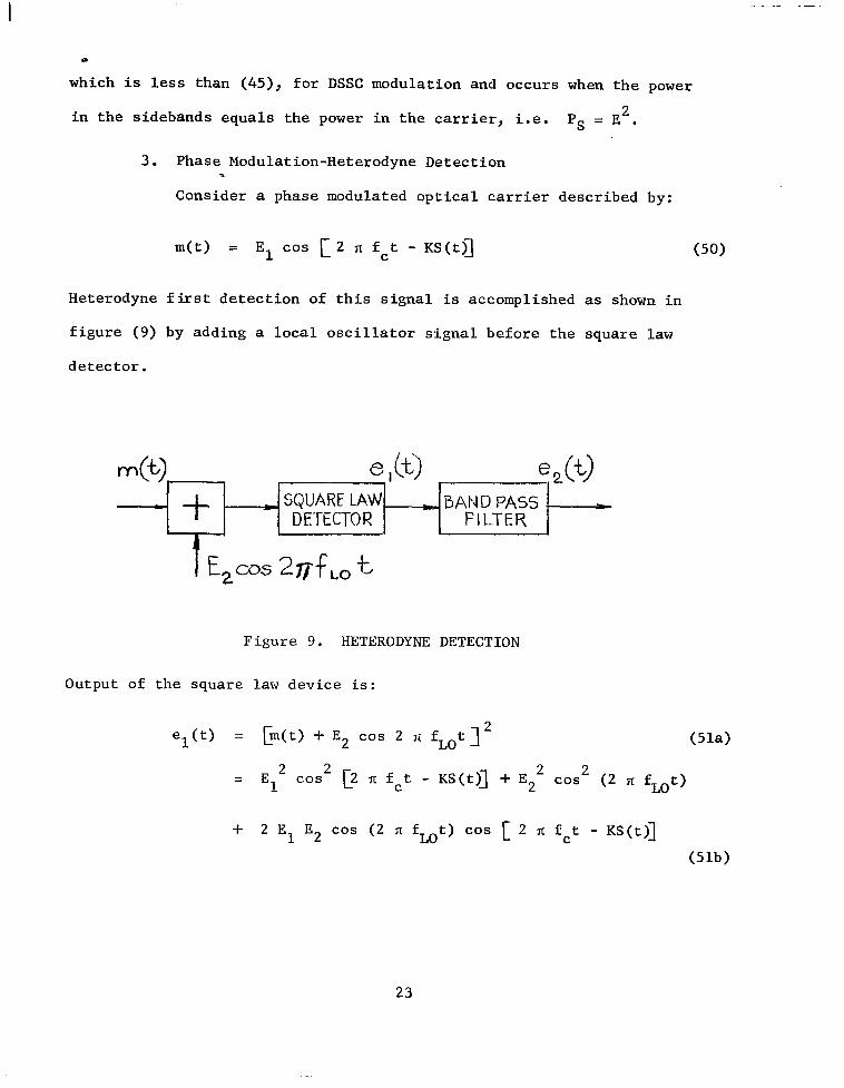
3. Phase Modulation-Heterodyne Detection 1
Consider a phase modulated optical carrier described by:
m(t) = El cos [2 x fct - KS(t)] (50)
Heterodyne first detection of this signal is accomplished as shown in
figure (9) by adding a local oscillator signal before the square law
detector.
Figure 9. HETERODYNE DETECTION
Output of the square law device is:
e,(t) = [m(t) + E2 cos 2 JI fLot] 2 (51a)
E1 2 = cos 2 p n fct - KS(t)l + E22 cos2 (2 n fLot)
+ 2 El E2 cos (2 x fLo t) cos [ 2 II fct - KS(t)]
(51b)
23

Applying an argument similar to that used in the DSSC modulation case,
output of the bandpass filter following the first detector is the
difference frequency.
e,(t) = El E2 cos p IC (fc - fLo)t - KS(t)7 (52)
The output signal to noise is given by the ratio of the difference fre-
quency average power to the average noise power incident on the detector
and is:
(3 out = (El E2)
2
k(E22+E12) B
=
A plot of (tkut versus 2 is shown in Figure 10.
(53)
Figure 10. SIGNAL/NOISE HETERODYNE DETECTION
24
The maximum signal to noise is given by:
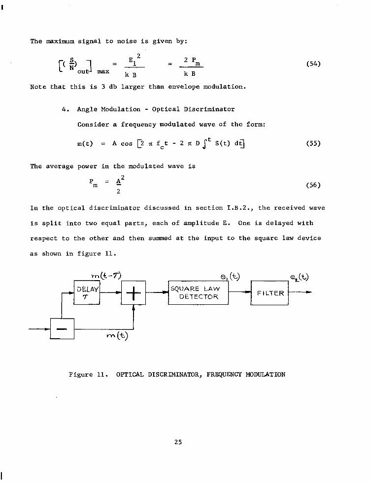
Note that this is 3 db larger than envelope modulation.
4. Angle Modulation - Optical Discriminator
Consider a frequency modulated wave of the form:
m(t) = A cos p n fct - 2 R D J' S(t) dg
The average power in the modulated wave is
'rn = A2 2
(54)
(55)
(56)
In the optical discriminator discussed in section I.B.2., the received wave
is split into two equal parts, each of amplitude E. One is delayed with
respect to the other and then summed at the input to the square law device
as shown in figure 11.
h-+-T) e,(t> ~.L(t - DELAY-
T =-+ ) SQUARE LAW
DETECTOR - FILTER c
1
- m &)
Figure 11. OPTICAL DISCRIMINATOR, FREQUENCY MODULATION
25

If the power split is equal, E = A .
ii- 2
Each wave component is described respectively by
m,(t) = E cos p x fct - 2 fi D St S(t) dq Wa)
t -7
m,(t) = ml(t - 7) = E cos p fi f,(t - 7) - 2 x Dl S(t) dt]
(57b)
Output of the first detector is
e,(t) = [m,(t) + m2 (tFJ2
which from previous analysis, (34) is:
e2(t) * 2 E2 x D T S(t) = A2 nD,r S(t)
The output signal to noise is:
(58)
(59)
($ = A4fi2 D2 i2 P 2fi2 A2 D2~2 P 2
S = S = (4* D2 72 pS pm (60) out k B A212 k B kB
If s(t) = cos (27r fmt) then Ps = l/2 and
= 2312D272 Pm = 19.6 D2 72 L Pm
i-ii- kB (61)
As shown previously, for 10% linearity, D T < l/8; and D 7 -C l/4 to make
the detector output a non-decreasing function of the input. Thus since,
26
sin (2 SC D 7 cos w,t) = 2 Jl (2 SC D 7) cos w,t - 2 J3(2 'JC D I-)cos Wmt + . .
(62)
Jl(x) is a maximum for X = 1.8 and
2 J1(1.8) =, 2 x 0.582 = 1.164 Thus for D 1.8 7 = 5 = 0.286, maximum
signal to noise output is
[( i ) ] max = 0.675 k (63) out
For a phase modulated wave, the analysis differs by the substitution:
K r (t) = 2 TI D [ S(t) dt (64)
and hence, the output of the bandpass filter is
e2 (t> A2 = A2 fi D 7 S(t) = j- K .T d r (t)
dt (65)
Adding the integrator after the filter as shown in figure 12 gives:
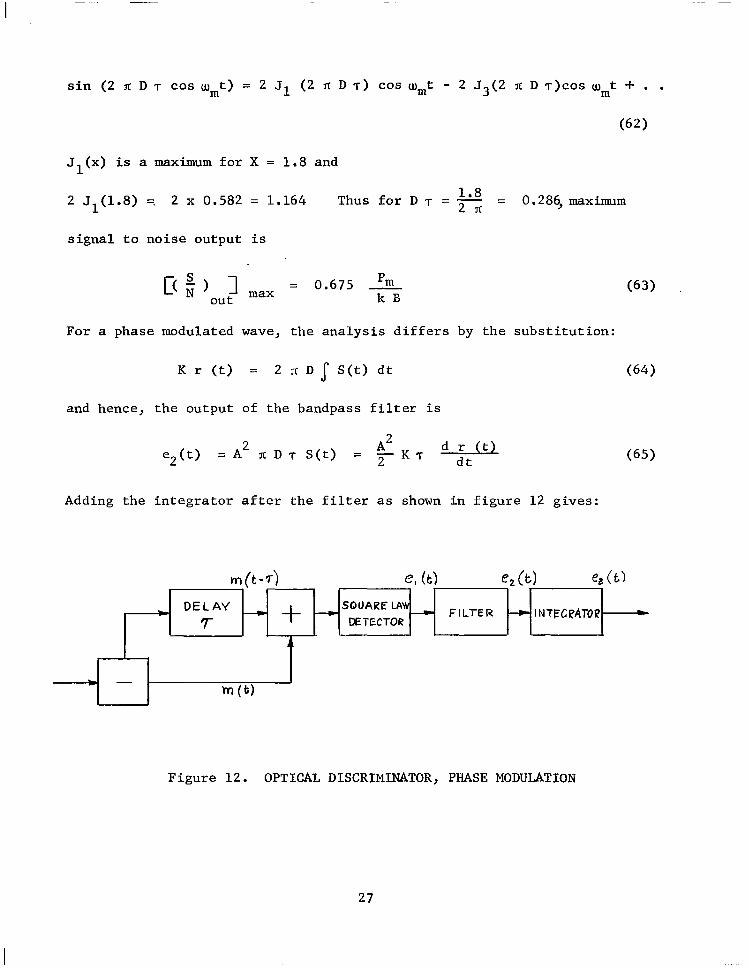
m(t-71 e, (tl e2 Ct) e3 W
- OELAY - + - SQUARE LAW 4
7 DETECTOR - FILTER --+ INT!3IiP~TOP
A
Figure 12. OPTICAL DISCRIMINATOR, PHASE MODULATION
27

e,(t) A2 = - K -r r (t) 2 (66)
This is the signal at the output of the integrator. The noise passes
through the integrator and since H(f) = L j 2flf ' and
no2 (t) = Jf2 $;(z)f;f2 = k A2 ~~~ $$ (67a)
fl 2 (2n>2 fl
k A2 L-1 1 A2 k B =- 8 n2 fl f2 = 8fi2fl f2
since B = f2 - fl
(67b)
The signal to noise output therefore is:
(;I = A4K2 .r2Pr = 231~ A2 K2 72 P, fl f2
out 4.A2 k B (68a)
kB
831~ flf2
= 431~ K2 ,r2 fl f2 P, Pm (68b) kB
If r(t) = cos wmt, P, = l/2 and the equivalent D = K fm. In addition if
$ < -c 1.. f f = f2. , 12 m Under these conditions m
( fi Lt
= 2fi2K2T2f2 'rn m kB
(69)
For maximum ( g ), D 7 = 0.286 = K fm I- therefore:
= 2 n2 (0.286)2 Pm = 1.61 P
kB k: (70)
28
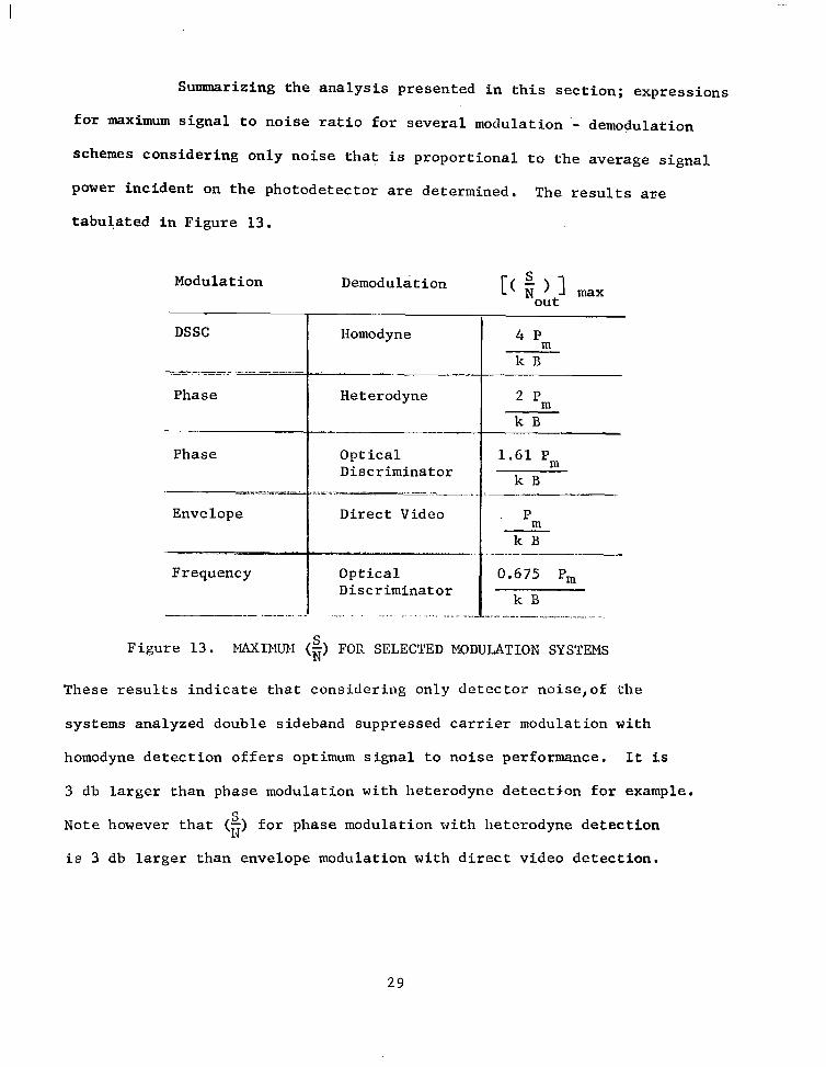
Summarizing the analysis presented in this section; expressions
for maximum signal to noise ratio for several modulation'- demodulation
schemes considering only noise that is proportional to the average signal
power incident on the photodetector are determined. The results are
tabulated in Figure 13.
Modulation Demodulation Cc+)1 max out
-- -__-
Phase
Discriminator
Direct Video
Discriminator
Figure 13. MAXIMUM (;) FOR SELECTED MODULATION SYSTEMS
These results indicate that considering only detector noise,of the
systems analyzed double sideband suppressed carrier modulation with
homodyne detection offers optimum signal to noise performance. It is
3 db larger than phase modulation with heterodync detection for example.
Note however that (i) for phase modulation with hetcrodyne detection
is 3 db larger than envelope modulation with direct video detection.
29

The (3 eXpreSSiOnS are Written in terms of Pm, the average power in the
modulated wave. If a particular hardware implementation of one of the
systems causes a variation in Pm as compared to another approach, con-
clusions drawn from the relationships listed in Figure 13 do not hold.
For example, transmitted reference homodyne or heterodyne schemes usually
involve a 3 db loss of modulated wave signal due to the geometry of
implementation. This is not common in a direct video detection scheme.
It is not intended that this analysis indicate the best modulation-
demodulation system for any given application. Objective of this con-
tract is to analyze an FM optical communications system and compare it
with other useful techniques. This analysis contributes to that objective.
D. Effects of Additive Noise Before Detection
The previous analysis of section I.C. treats system performance
in terms of noise generated in the square law detector. Another source
of noise for optical communications systems is additive background noise
such as direct or reflected sunlight. Normally due to optical and spatial
filtering, systems are not background noise limited. The analysis of this
section treats the performance of amplitude and phase modulated systems
in the presence of additive noise. The noise spectrum is described by
n(t) = p,(t) cos 2 J[ fct + q,(t) sin 2 JL fct (71)
where n(t) is bandpass, stationary, white noise of amplitude density No
and bandwidth B. Under these conditions p,(t) and q,(t) are low pass
30

white noises of amplitude density ANo and bandwidth 5. Further:
s O3 n2(t) dt = J w p 2 “q 2(t)dt= s m .j:N (f)12df = 2 No2 B -00 -co n (t> dt = J-m n -a3
(72)
With these definitions the analysis proceeds.
1. Amplitude Modulation
Consider a wave amplitude modulated by a signal S(t),
described as: m(t) = A [l + K S(t)l cos 2 fi fct (73)
where 1 S(t) \,, = 1 and K 5 1.
The modulated wave plus the additive background noise is
m(t) + n(t) = p -I- AKS(t) + pn(t)] cos 2 fl fct + qn(t) sin 2 fl fct
(74)
If this combined wave is incident upon a square law detector followed
by a low pass filter, the output of the filter is:
co(t) = l/2 [[A + AKS(t) + pn(t)12 + qn2(t)j (75a)
co(t) = l/2 A2 + 2 1 A2K2S2(t) + $ pn2(t) + $ qn2(t)
+ A2 KS(t) + A p,(t) + AKS(t) p,(t)
(75b) Assume the conditions A > > p,(t) and K < < 1; so that:
e,(t) e 2 L A2 + A2 KS(t) + A p,(t) = A2[ $ + KS(t) + vj (76)
31

The output consists under these conditions of a DC term, that is ignored,
the signal, KS(t), and noise, p,(t) .
A
2. Phase Modulation
A phase modulated wave, modulated by a signal S(t) is given by
(3) m(t) = A cos [ 2 fi fct - KS(t)] (3)
where IS(t),,\ = 1 and K is the phase deviation. The modulated signal
plus the additive background noise is described by:
m(t) + n(t) = A cos KS(t) cos 2ti fct i- A sin KS(t) sin 2rc fct
+ p,(t) cos 2 II fct + q,(t) sin 2 fi fct (77)
where the expansion cos (A-B) is applied. (77) may be written in the form:
m(t) + n(t) = v(t) cos [2 It fct - 0(t)] (78)
where 112
v(t) = {[A cos KS(t) + pn(t)7' + p sin KS(t) + qn(tq2J (79)
and 0 (t) = tan-l [A A sin KS(t) + q,(t) COS KS(t) -I- pn(t) ] (80)
An ideal phase detector has as its output e(t). Since the desired signal
is KS(t), the noise at the output may be described by
en(t) = 0 (t) - KS(t) (81)
Writing tan en(t) = tan 0 (t) - tan KS(t) (82) 1 + tan 8 (t) tan KS (t)
which after some manipulation may be written
32
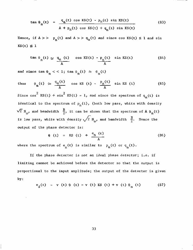
tan en(t) = q,(t) ~0s KS(t) - p,(t) sin KS(t) (83)
A + p,(t) cos KS(t) + q,(t) sin KS(t)
Hence, ifA>> p,(t) and A > > q,(t) and since cos KS(t) s 1 and sin
KS(t) s. 1
tan en(t) 3 4, (t) cos KS(t) - p,(t) sin KS(t)
A A
and since tan 8 n < < 1; tan 0,(t) 2 en(t)
thus en(t) % 4,(t) cos KS (t) - pn(t) sin KS (t) A A
(84)
(85)
Since cos2 KS(t) + sin2 KS(t) = 1, and since the spectrum of q,(t) is
identical to the spectrum of p,(t), (both low pass, white with density
fi No> and bandwidth 4, it can be shown that the spectrum of A e,(t)
is low pass, white with density B No, and bandwidth 2. Hence the
output of the phase detector is:
e W = KS (t) + en (t) A
where the spectrum of e,(t) is similar to p,(t) or s,(t).
(86)
If the phase detector is not an ideal phase detector; i.e. if
limiting cannot be achieved before the detector so that the output is
proportional to the input amplitude; the output of the detector is given
by:
e,(t) = v (t) 8 (t) = v (t) KS (t) + v (t) en (t) (87)
33

where v (t) is given by (79) which may be expanded to:
V(t) = {A2 + sbn(t) cos KS (t) + q,(t) sin KS (ta + pn2(t)-kqn2(t)] 112
(8%
Thus if A > > q,(t) and A > > p,(t), v (t) may be written
v(t) = A[l+ 2 Pn(t) cos KS (t) + 2 $p A A
sin KS(tql'2 (894
2A[l + 'n@) cos KS (t) qn(t) sin KS(tu (89b) A A
This indicates that the phase detector without limiting produces noise
amplitude modulation of the signal output. The degree of modulation is
inversely proportional to the input signal to noise voltage ratio which is
assumed to be large.
3. Comparative Evaluation
Comparing equations (86) and (76), the detector output for
optimal phase modulation and amplitude modulation respectively, note that
if A > > n(t); i.e., if the input signal to noise ratio is large enough;
both AM and PM have the same output signal to noise ratio for the same
K and A. However (76) was derived under the condition that K < < 1. If
this condition is not met the output contains more noise due to the term
AKS(t) p,(t) which was neglected in comparison to the term A p,(t). No
restriction of this sort is placed on the derivation of equation (86).
Therefore as K becomes larger, PM has an advantage over AM, in the
34

presence of additive background noise, for the same K. Obviously if a PM
system can be achieved, in practice, with a larger value of K than can be
achieved in an AM system, the PM system has a larger output signal to
noise ratio for the same input signal to noise ratio.
II. Experimental Study
A. 45' Y Cut ADP Modulator
1. Electra-optic Material
The transverse Pockels effect is chosen for the electro-optic
modulator because of the dependence of the phase retardation upon the
length to thickness ratio (L/t) of the crystal. As discussed in section
I.A.3. the required drive voltage for a fixed ratardation is inversely
proportional to the L/t ratio. A modulator with a relatively low drive
voltage requirement is therefore feasible. There are a variety of electro-
optic materials suitable for transverse modulators at visible wavelengths.
Specifically potassium dihydrogen phosphate (KR2P04) and its isomorphs,
KD2P04 and NH4 H2P04 have found widespread use in laser technology. These
are class E m crystals that have relatively large linear electro-optic
coefficients. Values of r41, which determines performance of these
crystals as transverse modulators, are given in figure 14 .
3. Ott, J. H. and Sliker, T. R. "Linear Electra-Optic Effects in KH2P04
and its Isomorphs" JOSA, Vol. 54, Nr. 12, pp. 1442-1444.
35

Material
KH2p04
m4H2PC4
Abbreviation Electra-Optic Coefficient r41
ww 8.77 + 0.14 x lo-l2 m/V
@W 24.5 f 0.4 x lo-l2 m/V
XD2p04 WP) _ 8.8 + 0.4 X lo-l2 m/V
(83% - 92% deuterated)
Figure 14: Electra-Optic Coefficient, r41, of Selected
Class 42m Materials at 546 nm.
Of these materials, ADP is the obvious choice for a transverse modulator
due to the large electro-optic coefficient. An additional feature of ADP
1s the availability of relatively large , good optical quality crystals
at low cost. For these reasons ADP is used as the modulator material on
this contract.
2. Modulator Configuration
A transverse modulator in ADP employs a 45OY cut crystal
as shown in figure 15(a). For phase modulation of an incident linearly
polarized wave the Y axis of the crystal is oriented either parallel
or perpendicular to the polarization axis of the incident wave. The
central ray of the light beam propagates through the crystal in the XZ
plane at 45' with respect to the Z axis. The field is applied to the
crystal parallel to the Y axis. Two modulator crystals were used during
the experimental work, with length to thickness ratios of 8 and 4
36

I Y AXIS
-Z AXIS
X AXIS
Figure 15A. 45O Y CUT ADP CRYSTAL
._
‘_
y:.. _’
Figure 15B. MODULATOR CRYSTAL HOLDER
37

respectively. The crystals are cut and polished from 45' Y rod of dimen-
sions: 3.2 mm. x 6.4 mm x 25.4 mm. Narrow dimension of the rod is along
the Y axis. To prevent fogging of the polished surfaces, glass plates
are applied to the end faces of the crystal with an index matching cement.
The crystal is held between brass electrodes of dimensions 3.2 mm. x 6.4
mm, x 25.4 mm. that are clamped in a plastic holder (see Figure 15b.).
The entire assembly is mounted in a fixture that rotates about the propa-
gation plane of the incident light beam.
3. Modulator Performance
Performance of the L/t = 8 modulator was measured in a
resonant circuit configuration at 50 MHz modulation frequency and in an
untuned circuit at baseband, (0 - 10 MHz) modulation frequencies. The
L/t = 4 modulator was operated only in the resonant circuit configuration.
The capacitance of the crystal and electrode structure is
determined by the combination of the uniform and fringe fields. The
uniform field capacitance may be calculated from the familiar parallel
plate formula:
C = A P ‘0’ d
where s = 8.86 x lo-l2 in mks units 0
E = 16, dielectric constant of ADP
A = contact area of the electrodes
d = electrode separation
38
(90)

II -
For the L/t = 8 crystal this is:
C = 8.86 x -6 P
lo-l2 x 16 x 3.2 x 25.4 x 10 -12 = 3.6 x 10 farads 3.2 x 10⁻³
The fringe field capacitance is most easily determined using a graphical
approximation. Flux lines and equipotentials for a half section of the
crystal are shown in Figure 16. The capacitance per unit length is given
by CL=eoe Nf (91)
N P
where N f is the number of graphical flux divisions
Np is the number of potential divisions.
---- FLUX IAN ES EQL)~~OTEWTIALS
Figure 16. GRAPHICAL ANALYSIS, FRINGE FIELD CAPACITANCE
39

The total fringe capacitance is CL times the crystal length.
cf = 2 x 8.86 x lo-l2 x 16 x 0.5 x 25.4 x 10 -3 = 3.6 x lo-l2 farads
Total capacitance is Ct = Cp + Cf = 7.2 x 10 -12 farads (92)
This value of capacitance agrees very closely to a value determined by a
bridge measurement on the crystal.
A series tuned R, L, C resonant circuit is used to impress
the 50 MHz modulation carrier on the ADP crystals as shown in Figure 17.
-
Figure 17. MODULATOR RESONANT CIRCUIT
Parameter values for the L/t = 8 crystal are: C = 7.2 x
lo-l2 farads, L. = 10 -6 1 henries, R = 51 ohms. The resonant frequency
is given by
f 1 = m 112
= 59.4 x lo6 Hertz 2x (LiC)
(93)
40

The actual resonant frequency was measured at 53 MHz, due apparently to
distributed capacitance in the circuit. The Q of the resonant circuit
is
Q = 2srfmLi = 65 . (94) R
The voltage across the crystal at the resonant frequency is
Vi = 1 xc = EXc =QE Z
(95)
where E is the generator terminal voltage applied to the resonant circuit,
xc the reactance of the crystal, Z the circuit impedance, and I the
generator current. Figure 18 is a plot of crystal voltage and resistor
power dissipation as a function of generator terminal voltage for several
values of circuitry Q. The generator used to test the modulator, a
Johnson-Viking transmitter, has a capability of driving the circuit at
18 watts. From the chart, for a circuit Q of 6.5 the terminal voltage
is 30 volts and the crystal voltage is 195 volts. Capacitance of the
L/t = 4 crystal is 3.5 x 10 -12 farads. It resonates at 51 MHz with a
2.8 x 10 -6 henry inductor. Circuit Q determined by (94) is 18. For a
driving power of 1 watt, voltage across the load resistor is 7.8 volts.
The crystal voltage is V = QE = 140 volts. The high value of Q gives
large crystal voltages at reduced bandwidth.
The voltage induced phase deviation in the transverse ADP
modulator is given by equation (16) derived in section I.A.3.
41

Watts
30
Q= 10 Q = 6.5 , Q=5
= 6-5 Q=5
20 30 40 5b 66 7b 8b
Terminal Voltage
Figure 18. CRYSTAL VOLTAGE DISSIPATION AS A FUNCTION OF TERMINAL VOLTAGE
300 &
2 l-l
250 g t-l cu .u
150
100
50
42

*#i = prql Vno3 4 C 3 (16)
Value of r4,1 at 0.546 microns is given in Figure 14. The ordinary index
of refraction n = 1.53. 0
The phase deviation as a function of crystal
voltage and L/t ratio is
A@ = 1.01 x 10 -3 v 4 (96)
For L/t = 8, and V = 195, A @ = 1.58 radians. Maximum frequency
deviation at the 53 MHz modulation frequency is
D =A$f = 84 MHz m (97)
Evaluation of modulator performance depends upon successful demodulation.
Test data for 50 MHz modulation is included in section 1I.B. under
demodulator breadboard analysis.
Use of the ADP crystals as baseband modulators, i.e. in
the frequency range O-10 MHz; involves impressing the driving voltage
directly upon the crystal as shown in Figure 19. The high gain broad-
band amplifier required for this application is discussed in section
Figure 19. BASEBAND MODULATOR
43

III. A. 3. Peak to peak drive voltages on the order of 200 volts are
possible with the driver. This gives a phase deviation for the L/t = 8
crystal of 1.61 radians.
Thermal strain effects in the electro-optic crystals
induce birefringence that degrades intensity modulator performance. 4
In addition to this effect, 45' Y ADP has a natural birefringence in the
XZ plane that is a function of crystal rotation about the propagation
axis. These effects do not degrade performance of a system that uses
a demodulator that is sensitive only to instantaneous frequency devia-
tion. Heterodyne first detection followed by an amplifier, limiter,
and frequency discriminator second detector is such a system. Since
the thermally induced variations or mechanical vibration about the rota-
tion axis occur at a low frequency, typically less than 100 Hertz, even
for large phase deviations of several radians the instantaneous frequency
deviation is small and filterable. Experience with the two ADP mdoulators
confirms this: whereas intensity modulation is severely degraded by
heating of the crystal; angle modulation shows no visible effect. The
crystal may be rotated several degrees about the propagation axis, also
with no visible effect upon angle modulation but with deleterious effect
upon intensity modulation.
4 Kaminow, I.P. "Strain Effects in Electra-optic Light Modulators" Applied Optics Vol. 3, Nr. 4, pp. 511-515.
44
The preceding discussion demonstrates the usefulness of a
45' Y cut transverse ADP modulator in a variety of operational configura-
tions. The L/t = 8 crystal is chosen as the optimum modulator for this
contract due to the large phase deviation obtainable with moderate drive
voltage.
B. Demodulator Breadboards
Optical breadboards of homodyne, optical discriminator, and
heterodyne demodulators were constructed and tested to experimentally
verify modulator performance. The test results confirm the conclusions
drawn in the analytical study portion of the program; specifically, that
the homodyne and optical discriminator techniques are amplitude noise
sensitive.
1. Homodyne
Arrangement of the homodyne optical breadboard is shown in
Figure 20. The interferometer assembly is mounted on 18 mm. thick alumi-
num surface plate for stability. The beamsplitter is a mirror type with
30% reflectance and has surfaces parallel to 20 seconds of arc. The
interferometer mirrors are dielectric coated flats with maximum reflec-
tivity at the laser wavelength and are mounted on holders with three point
adjustment for ease of alignment. The reference beam mirror is mounted
on a slide carriage, adjustable along the optical axis. The Pockels modu-
lator is contained in a rotatable holder placed on the optical axis of
the signal arm of the interferometer. Direction of rotation is about the
45

I I
SURFACE PMTE f MIRRQR -----w--- ----- I
Figure 20. HOMODYNE OPTICAL BREADBOARD
optical axis. The laser is a Spectra Physics model 131 operated in the
hemispherical mode without external beam forming optics. Power output
is 0.5 milliwatt and beam divergence is less than 0.7 milliradians. The
polarizer is a Nicol prism. The laser, polarizer, and interferometer
are rigidly mounted to a 10 cm. wide, dual rail optical bench. The photo-
multiplier detector is an RCA experimental type C70042 CP and is mounted
on a separate stand at right angles to the optical bench.
There are several important factors involved in the opera-
tion of the homodyne demodulator. It is essential for good mixing action
on the photodetector that the signal beam and the reference beam be
exactly parallel and superimposed. The degree of alignment is checked
46
by noting the interference fringes between the two beams displayed on
a white card at the detector location. Two or three wide dark fringes
within the beam pattern indicate adequate spatial phasing of the two
lasers. Relative time phase between the signal and reference waves is
adjusted to n 2 , where n is a small integer. This is accomplished in 2
one, or a combination, of three ways; angular orientation of a quarter
wave retardation plate in the signal arm, angular orientation of the
naturally birefringent 45 degree Y cut ADP crystal, or adjustment of the
reference beam optical path length. In the breadboard model there is
sufficient vibration of the mirrors to give a time average of the optimum
alignment conditions.
A useful feature of the homodyne breadboard is the double
pass modulator configuration. Both the 8 to 1 and 4 to 1 length to
thickness ratio crystals were used in the assembled breadboard. Phase
retardation for the 8 to 1 crystal at 5 watts drive is 1.84 radians; for
the 4 to 1 crystal at 1 watt drive power the phase retardation is 1.12
radians. Both values of phase shift exceed the conditions for linear
modulation, i.e. K < < 1. For both modulators, detected signal amplitude
in the breadboard system is insensitive to drive power variations due to
saturation caused by the nonlinearity.
Input to the photomultiplier detector is filtered both
optically and spatially to prevent current saturation. Output of the
detector is fed to a UHF receiver consisting of an APR-4 receiver unit
47

and a 541 Tektronix oscilloscope and/or a Polarad spectrum analyzer. The
demodulated sine wave and frequency spectrum for 5 watts drive power at
52 MHz on the 8 to 1 crystal are shown in Figure 21. A drift in wave
amplitude is noticeable as the RF power heats the crystal. This is com-
pensated by rotation of the crystal. Amplitude sensitivity of the
homodyne system is demonstrated by inserting neutral density filters in
the optical path between the interferometer and the detector.
Experience with the homodyne demodulator breadboard
demonstrates: sensitivity of the system to vibration through variations
in the relative optical path length difference between the two arms of
the interferometer, non-linear detection for large values of phase devia-
tion, and sensitivity of the system to amplitude fluctuations in the
transmitted beam. The first item is corrected by rigid mechanical design
of the interferometer. The analysis performed during the analytical
study predicts non-linear detection for large values of phase deviation,
K; and the amplitude sensitivity of the system as demonstrated in the
experimental model.
2. Optical Discriminator
A diagram of the optical discriminator breadboard is shown
in Figure 22. The interferometer assembly is mounted on 18 mm. thick
aluminum surface plate for mechanical rigidity. The maximum path length
difference between the two arms is 60 cm.; and it is adjusted by motion
of a mirror mounted on a slide carriage assembly. Separation of the
48

B - Spectrum Analyzer
Center Frequency 50 MHz RF Drive 5 Watts L/t = 8
A- 52 MHz Modulation
ADP Crystal Drive Power - 5 Watts L/t = 8
Figure 21. HOMODYNE DETECTED SIGNAL
49

- - - -- - -- - - -._- -__. - - SURFACE PLATE
BEAMSPLITTER
Figure 22. Figure 22. OPTICAL DISCRIMINATOR BREADBOARD OPTICAL DISCRIMINATOR BREADBOARD
fixed mirror and the mirror beamsplitter, L1 is 5 cm; separation of the
movable mirror and the beamsplitter, L2 (max.) = 35 cm., L2 (min.) = 2 cm.
The.mirrors are dielectric coated flats with maximum reflectance at the
laser wavelength. They are installed in three point adjustable mounts
for ease of alignment. The mirror type beamsplitter is the same one
used in the homodyne breadboard. The laser is a Spectra-Physics model
131 operating in the hemispherical mode. The laser, Nicol prism
polarizer, modulator, and interferometer are mounted on the 10 cm.
optical bench. The photomultiplier detector, type C70042CP, is mounted
on a separate stand perpendicular to the optical bench. A quarter wave
plate is placed in the adjustable length interferometer arm on a rotatable
50

I -
holder. The modulator may also be rotated about the optical axis.
Several conditions must be satisfied for satisfactory
operation of the optical discriminator. As in the case of homodyne
detection the two beams must be exactly parallel and superimposed for
good mixing action on the photomultiplier. Interference fringes are
observed to determine optimum spatial phasing of the two beams. The
condition fc 7 = II 4' (equation 27)' is satisfied by rotation of the
quarter wave plate. The other condition that must be satisfied is
wm 2 T < 2.8 for K < 0.28 or W, 7 < 4K for K> 0.28. Recall that
these conditions are derived from the requirements for linear detection
(equations 32 ff). The value for K is given by (96)'
-3 & K=lO Vt (96)
The L/t = 4 modulator crystal is used in this work, so K = 4 x 10m3V.
The angular frequency for 51 MHz modulation is
wm =2flfm = 3.2 x lo8 radians/set. (98)
The maximum delay time, 7maxJ is:
7 = 2 CL2 max - LJ = 2 x UYg sec. IMX
C
The minimum*delay time, 7minJ is:
(99)
T = min 2 C L2(min) - LJ = 1.25 x lo-' sec. (100)
C
51
where c is the velocity of light, 3 x lo8 meter/set.
Therefore:
Wm7max = 0.64 radians
1 (101)
Wm 'min = 0.4 radians
In order to determine which condition on urn7 applies, it is necessary to
computer K for the drive voltages used. Data is taken at three input
power levels: 0.5, 2, & 5 watts. Voltage across the crystal with a Q
of 18 for a circuit R of 50 ohms is 90, 180, and 284 volts respectively.
The corresponding K's are shown in Figure 23.
Drive Power
(a) 0.5 watts
(b) 2.0 watts
(c) 5.0 watts
Applied Voltage on Crystal
Retardation K
90 volts 0.36 2.18
180 volts 0.72 1.09
284 volts 1.14 0.704
Figure 23. PARAMETERS FOR L/t = 4 Crystal in Optical Discriminator
In each case K> 0.28, therefore wrn 7 c4i must apply for linear detection.
In each case this condition is satisfied for all values of wrn 7. Figure
24 shows the detected sine wave for 52 MHz modulation at the three values
of drive power for three values of wm 7. The receiver is an APR-4 receiver
unit in combination with 541 oscilloscope. 'The data shows a trend toward
increased output amplitude proportional to drive power and wrn7 as predicted
by the analysis' (equation 34); although comparison of specific data is
52

0.5 Watts 2 Watts 5 Watts K = 0.36 K = 0.72 K = 1.14
Minimum Path Length u.1~7 =.0.4
Mean Path Length wrn7 = 0.52
Maximum Path Length UI~T = 0.64
Figure 24. OPTICAL DISCRIMINATOR DETECTED SIGNAL

not in agreement. This inconsistency is due to instability in the bread-
board caused by mechanical vibration of the mirror mounts. Also the
range of wm7 is limited by the mechanical layout on the surface plate.
Sensitivity. of the optical discriminator to amplitude variations is
observed by inserting neutral density filters in the beam between the
modulator and beamsplitter. No attempt was made to observe the AM rejec-
tion at the modulation frequency, w,.
3. Heterodyne
Arrangement of the optical breadboard for heterodyne
detection is shown in Figure 25.
--m-- -------
I
SURFACE PI.hTE APR-4
CoNVERTE t
ADP CRYSTAL I 4 SP-119 LASER I l\. + PMJ
BEAM COMBlhlER f I I
Figure 25 HETERODYNE OPTICAL BREADBOARD
IMK III AMP
The transmitter unit consists of a signal laser, reference
laser, Pockels modulator, and right angle prism beam combiner. The lasers
are Spectra-Physics model 119, chosen for single mode and stable frequency
operation. The temporal coherence of the output radiation is achieved by
54

use of a stabilized optical resonator of such short length that only a
single mode can be sustained. The plasma tube is mounted in an invar
resonator structure having bi-metallic temperature compensation. One of
the dielectric resonator mirrors is mounted on a piezo-electric element
which is voltage controlled for mirror spacing with resultant control of
laser frequency. A photodetector and servo controller permit locking of
the mirror drive voltage to the Lamb dip region of the lasing mode. The
resonator and plasma tube are housed in a temperature controlled oven for
thermal stability. Surrounding the oven is a mu-metal cover which shields
the invar resonator from magnetostrictive modulation effects caused by
stray external magnetic fields. These lasers are servo locked to a fixed
offset difference frequency of 200-300 MHz. The phase modulation on the
signal carrier is transferred to the difference frequency upon square
law detection of the two signals at the receiver.
The breadboard receiver unit consists of a C70042CP photo-
multiplier detector, APR-4 tuning unit modified to a 60 MHz intermediate
frequency, and a LEL model INK amplifier, limiter, discriminator unit.
The phase modulated difference frequency is converted down to the
intermediate frequency of the FM receiver unit and subsequently detected.
In this experimental work a subcarrier modulation in the range O-2 MHz is
used in order to stay within the 3 db bandwidth of the receiver units.
Successful results obtained with the experimental model i.e. mixing of
the two laser frequencies to obtain the difference frequency, and detec-
tion of subcarrier modulation, led to an early decision to implement this
55

heterodyne detection method in the experimental breadboard. Detailed
discussion therefore of the experimental data is included in following
sections of this report.
III. BREADBOARD SYSTEM
A. Hardware Description
A block diagram of the transmitted reference heterodyne laser
communications system is shown in Figure 26. There are three basic
elements of the system: the transmitter unit, the receiver unit, and the
modulation-demodulation electronics. Shown in the diagram is the implemen-
tation for single frequency subcarrier modulation. Operation of the system
is identical to that of the experimental system described in section II.B.3.
1. Transmitter Unit
Photographic views of the transmitter unit are shown in
Figure 27. Picture A is an exterior view showing the unit cover, colli-
mating telescope, and 7X spotting scope. Picture B is an interior view
showing the arrangement of the optical components: lasers, modulators,
beam combiner, and eyelens of the collimating telescope. Picture C shows
the transmitter unit mounted on the tripod at one of the experimental test
sites. The laser power supplies with integral servo controllers are placed
on the tripod base plate. The tripod is adjustable 360 degrees in aximuth
and approximately 30 degrees in elevation. Picture D shows the detail of
the mounting adjustment for the lasers.
The baseplate for the transmitter unit is fabricated from
56

I -
. t Signal Pockcls
GeIU?ratOr -c Amplifier ---c
Modulator -L
Driver Modulator
I
119
Laser
I
Beam
Combiner
Secondary
Collimator
Transmitted
Beam
TRANSMITTER
RECEIVER Received
Photomultiplier ,e- Telescope ,G Beam
1
Converter
I
t IF
Ampl i fi er
I
Limiter
CR0 - Amplifier N- Discriminator
Figure 26. TRANSMITTED REFERENCE HETERODYNE LASER COMMUNICATIONS SYSTEM
57

C-Tripod Assembly
B-Transmitter Unit
A-Optical Layout D-Adjustments
Figure 27. BREADBOARD MODEL - TRANSMITTER UNIT
58

18 mm. thick aluminum surface plate. This is a strain relieved metal that
resists warping and bending. The lasers are mounted to carrier plates on
three thumbscrew legs that permit adjustment of laser height and angle of
the case with respect to the baseplate. The carrier plates slide on the
baseplate surface and are oriented by three thumbscrew adjustments that
allow translation of the laser and angular adjustment in the plane of the
baseplate. Thumbscrew stops are provided for locking the vertical and
horizontal adjustments and in addition, two hold down clamps are provided
on the carrier plate at the front and rear of the case. Figure 27d shows
the constructional detail of a horizontal adjuster and the hold down clamp.
This method of mounting the lasers provides a versatile arrangement for
alignment of the beams with respect to each other and the external optical
components. The locks assure that alignment is maintained during normal
handling of the transmitter unit. Experience with this mounting arrange-
ment has proven it to be adequate for all adjustment procedures.
Details of the modulator holder are shown previously in
figure 15 b. The ADP crystal is wedged between two brass electrodes. A
small detent is machined on the back of the electrodes for keying with a
spring loaded ball check that is screwed into the plastic half shell. The
ball check maintains compression on the crystal through the clamping action
of the electrodes. The crystal can be rotated 100 degrees about the optical
axis when mounted in the holder. Electrical contact is made to the elec-
trodes on the ends opposite those shown in the picture. Twisted pair leads
59

are soldered directly to the end surfaces and bent aside to prevent inter-
ference with the laser beam.
Beam divergence of the model 119 laser without the colli-
mating telescope is 10 milliradians, with the collimating telescope it is
less than 0.3 milliradian. Both the signal carrier and local oscillator
lasers are used with the integral collimating optics. A secondary colli-
mating telescope is provided for spreading the combined output to one
milliradian beam divergence. One milliradian gives a one meter spot
size at one kilometer. The pointing precision required for a one milli-
radian beam divergence is 0.5 millimeter deflection at the end of a meter
long lever arm at the transmitter. This gives a shift of one half the
beam diameter at the target. The double collimator optics configuration
is chosen, so that highly collimated beams traverse the optical paths in
the interferometer; thereby minimizing optics lasers in the modulator
and insuring precise beam alignment. The secondary beam collimator is
a simple Galilean telescope. An exaggerated ray diagram is shown in
Figure 28. The parameters are defined as follows: dl is the diameter
of the objective lens, d2 is the diameter of the beam at range 7, x1 is
the,object distance, and x1 is the image distance. By similar triangles:
+ x1' I
7 x1 = d2
(102a) -a-i-
therefore: 1 '4 x.1 = - (102b)
d2-dl
60

Figure 28. SECONDARY BEAM COLLIMATOR RAY DIAGRAM
From the lens maker's formula:
1, x1 ++ = $1 x1
where f 1 is the focal length of the objective lens. Therefore:
I
x1 ? fl Xl
x1 - fl
(103a)
(103b)
Combining (102b) and (103b) and solving for xl:
x1 = c fl dl
(104) rdl - fl W2-dl>
Substituting design values for the breadboard system: r = 103m, fl =
-0.401m, dl = 0.044 m, d2 = lm: x1 = -0.397 meter. Spacing between the
eyelens and the objective lens is 1 x1( p lus the focal length of the
61

eyelens, f2* Let f2 = 0.047 m and:
6 = 1 X1 1 + f2 = 0.444 m (105)
A fine screw thread is provided on the eyelens mount to permit adjustment
of 6 to the optimum value given by (105).
Alignment of the optical components in the transmitter unit
is essential for good spatial mixing of the laser beams. The following
alignment procedure is recommended for optimum performance. Adjust each
laser collimating lens individually for minimum spot size on a white card
at 30 meters with all optical components removed from the transmitter unit,
i.e. modulator, beam combiner, and secondary collimator. Install the
beam combiner and align the carrier laser beam with respect to the base-
plate and the center of the circular exit aperture. Centerline of all
optics is 10.2 cm above the baseplate. Align the local oscillator laser
to the signal carrier laser by superimposing the L.O. laser beam on the
signal laser beam on a white card at 5 and 30 meters respectively. This
may be done simultaneously with the right angle combiner. Install the
modulator in the signal carrier laser beam path. The crystal is wedge
shaped i.e. the end faces are not parallel, so the signal carrier beam
will deflect away from the L.O. beam. With the crystal rotated in the
holder to operating position, adjust the signal carrier laser to the
center of the modulator crystal and superimpose it on the reference
beam at 5 and 30 meters. Install the secondary collimator if desired
and the system is aligned. Optimum mixing should be observed anywhere
62

B
Figure 29. BREADBOARD MODEL - RECEIVER UNIT
63

in the propagation path of the transmitter unit.
2. Receiver Unit
An overall view of the receiver unit is shown in Figure 29A.
It consists of a Newtonian telescope, 7X spotting scope, and a receiver
box. The telescope primary lens is an f/10, 10.8 cm diameter spherical
mirror. It is installed on a conventional three point mounting for ease
of alignment. The secondary mirror (mirror diagonal) is mounted on a
single, vertical post near the entrance to the tube. Interior details of
the receiver box are shown in Figure 29B. It contains a .field stop for
limiting the field of view of the receiver, the photomultiplier assembly
including a narrow band spectral filter, the converter chassis and the IF
amplifier chassis containing the limiter, discriminator, and video
amplifier.
Geometry of the receiver optics is shown in Figure 30.
d P Y’
‘&
fiJ 1 --_
--_-__-_ --- _ - ___ ___ ------ __
- - .-.--_.. _. -- _.____ -- _.__.._ - __..__..
------- __--- ---
\=I---
XMM
Figure 30. RECEIVER OPTICS GEOMETRY
64

The receiver beam angle is given by
8 -1 = 2 tan d4
ret T-q (106)
where d4 is the diameter of the circular field stop and f3 is the focal
length of the primary mirror. Design value for 8 is a milliradian and ret
since f 3 = 114 cm.
d4 ='recf3 = 1.14 millimeters
An adjustable iris diaphragm is used as the field stop in order to obtain
the design beam width as well as larger fields of view. The secondary
mirror is an elliptical diagonal of dimensions: 27 mm x 38 mm x 6.4 mm
thick. Blockage due to the beam diagonal is given by the projection of
the long dimension normal to the incident beam. The projected dimension
is given by
Y' = y cos (45O) = 27 mm. (108)
The effective collecting area of the mirror is given by
A 2 12 2 eff = * (d3 - y ) = 89.4 cm
where d 3 is the diameter of the primary mirror. The effective diameter is
that which gives Aeff and is d3' = 10.6 cm. It is apparent that the
diagonal blocks very little of the lens aperture. The diagonal may be
placed anywhere that it does not vignette the converging beam. By similar
triangles the maximum allowable distance from the center of the beam
65
diagonal to the plane of the field stop is given by:
X max = Y’ f 3 = 27.9 cm. (110)
d3
Since the field of view is very narrow, this holds for all beam angles.
The spectral filter used on the photomultiplier is designed
to the following specifications: bandpass 2.5 2, plus 1 z minus 0, at 0
6328 i, plus 1 A minus 0, transmission 35% minimum, blocked for S-20
response; diameter 2.54 cm. The filter is evaluated by mounting it on a
rotatable holder and measuring the transmission characteristics for the 0
6328 A HeNe laser line. Maximum transmission is measured to be 56% at an
incident beam angle of 2.5 degrees with respect to the normal. The filter
is mounted to the photomultiplier holder with a wedge spacer inserted to
give a 2.5 degree angle of incidence for the transmitted beam. The
transmission measurements are made at room temperature and vary at dif-
ferent temperatures.
The photomultiplier detector is an RCA experimental type
C70042CP. It is a ten stage, ruggedized, head-on type tube with S-20
response, curved photocathode, and internally potted dynode bleeder.
Current gain at minus 1500 volts anode potential is 4 x 10⁴, at minus
2000 volts it is 3.3 x 10⁵. The tube has low distributed anode circuit
capacity and small transit time fluctuations for 500 MHz response.
The converter is an LEL model RMP-l-250-70-60-08 receiver
module. It consists of an RF preamplifier unit and a converter unit.
The RF bandwidth is 70 MHz centered at 250 MHz. The intermediate frequency
66

.is 60 MHz and the IF bandwidth is 8 MHz. Converter gain is > 30 db and
noise figure at 256 MHz is 6.3 db. Impedances are 50 ohms. The IF
amplifier is an LEL model IMK-l-60-10-50. Center frequency of the IF
amplifier is 60 MHz and the 3 db bandwidth is 10 MHz. IF gain is 84
db. The discriminator peak to peak bandwidth is 15 MHz. Video ampli-
fier gain is 23 db. Noise figure of the amplifier is 2.6 db. Impedances
are 50 ohms.
3. Modulation Demodulation Electronics
The modulator electronics consists basically of a Hewlett-
Packard 606 signal generator, a Tektronix 514 video amplifier, and a
driver amplifier. A schematic of the driver amplifier is shown in
Figure 31. This arrangement permits subcarrier modulation from below
1 MHz to approximately 10 MHz on the light beam. The overall frequency
response drops off above 6 MHz. The driver amplifier consists of a
cathode follower, buffer input stage to obtain a good impedance match
between the pre-driver amplifier and the final. The final driver stage
consists of two 4Cx250B power tetrodes in parallel operating as a class
B amplifier. Gain of the modulator driver is 20 db. Nominal peak to
peak voltage input from the 514 amplifier is 50 volts, so the peak
swing on the modulator crystal is 500 volts. Interlock relays are
installed in the unit, as shown in figure 32, to provide.proper
sequencing of the tube potentials. The OFF-ON switch applies filament
voltage and grid bias to the tubes, activates the air blower, and applies
67

I zoov, ZOOM4
/ 1, \ B-w 3-
+2sov --SW
I? r 2 ,5
,- - “30 ‘V
Figure 31. ~Rnm3 AMPLIFIER SCHEMATIC

AT IOA
I I I
Figure 32. DRIVER AMPLIFIER CONTROLS
69

A
B
Figure 33. MODULATION ELECTRONICS
70
voltage to the screen interlock switch. The PLATE switch activates the
plate relay which applies B+ voltages to the chassis. It also closes the
interlock switch in the screen relay circuit. The SCREEN switch applies
voltage to the screen relay, which supplies screen voltage to the tubes.
Associated with each switch on the front panel is a pilot lamp that
indicates the ON position. A photograph of the driver amplifier chassis
is shown in Figure 33A. Power required for the amplifier is: 6 Vat at
9 amps filament supply, 350 Vdc at 100 ma screen supply, 1000 Vdc at 700
ma plate supply, and -30 Vdc grid bias supply. The filament and plate
relays operate from ac line voltage.
A block diagram of the modulation system for broadband
video modulation is shown in Figure 34.
I SUBCARRIER OscrLlAroR
Figure 34~ BROADBAND VIDEO MODULATION
71

The signal source is a 3 MHz bandwidth, vidicon television camera. It is
necessary to translate the video signal up in frequency to avoid the laser
servo noise spectrum in the detector output. This noise problem is dis-
cussed in detail in Section III.C.l. A Hewlett-Packard model 10514A
diode bridge mixer is used to amplitude modulate the video signal on the
subcarrier. Input impedance of the mixer is 50 ohms and maximum drive
current in the X port is 40 ma. An amplifier is required to obtain
optimum drive into the mixer. A schematic diagram of the pre-mixer is
shown in Figure 35. Figure 33B is a photograph of the chassis showing
the input filter and the bridge mixer. Input to the modulator driver
in the broadband video mode of operation is nominally 30 volts peak to
peak, so the peak drive on the ADP crystal is 300 volts. Voltage swing
of the individual video frequency components depends upon the depth of
modulation of the video on the subcarrier.
The demodulation electronics follows the FM discriminator
and video amplifier of the receiver IF amplifier. The signal at this
point, ignoring noise, is simply the subcarrier or in the broadband
modulation case, the subcarrier plus sidebands. In the wideband case
the detected waveform is first compensated by passing it through a low
pass filter. The waveform is then envelope detected. The detected video
signal is amplified and applied to a CRT monitor for display purposes.
72

l.5K 2.N ‘993
27UH
00
-Yr OK
T--G IO
*J-
820
!tJ ‘493
WI493
6V - +24
+ - 1 300 2w
‘=
Figure 35. MIXER PRE-DRIVER AMPLIFIER SCHEMATIC

B. Performance Analysis
1. Signal Considerations
Signal power received at the receiver in a one-way link is
given by
P ret ret = pm eear A
ret (111) A trans
where a is the atmospheric attenuation factor, A is the area of the ret receiver aperture, and A trans is the area of the transmitted beam in the
plane of the receiver. Assume that a < < 1, and that A >A trans ret' Substituting, (111) becomes:
'2 P ret = 'md3 ret 2 2
r eb
(112)
where eb is the transmitter beam divergence. The expression does not
account for optics losses in either the receiver or the transmitter.
Figure 36 shows Prec ret
for ranges from 1 to 5 kilometers assuming d; =
10.6 cm, Pm = 10 -4 watts, and 8 b = 10-3 radians.
Range (rj meters
103
2 x 10³ 3 x lo3 4 x 10³
5 x lo3
Received Signal Power (PE,","> Watts
1.12 x 10 -6
2.8 x 1O-7
1.24 x 1O-7 7.01 x 10 -8
4.48 x 1O-8
Figure 36. RECEIVED SIGNAL POWER AS A FUNCTION OF RANGE
74

Note that if the secondary collimator is removed, 8; = 0.3 x 1o-3 radians,
and P 'ret ret = 10 P=z.
Optics losses in the transmitter are due to the collimator
lens elements, the right angle prism beam combiner, and the modulator
crystal. Lens element losses are ignored because the laser output is
normally measured with the collimator in place. The beam combiner causes
a loss of one half of the available laser power or 3 db. A special prism
can be used as a beam combiner in an operational system to eliminate this
power loss. The modulator loss, since this is a phase modulator is
simply the light attenuation through the crystal. This is nominally
3 db. Since the output of the model 119 laser is usually greater than
100 microwatts, the assumption that Pm = 10 -4 seems valid even consider-
ing the transmitter optics losses. As the laser tube ages, of course,
Pm reduces proportionately.
The receiver optics losses are due to the reflection loss
of the primary and secondary mirrors and the transmission loss of the
narrow band filter. These losses are approximately 4 db. It is noted
later that receiver losses do not affect performance of background limited
systems, .since the background noise power is reduced proportionately to
the signal power.
The assumption that Q r ~1 is not necessarily valid at
relatively long ranges even under good seeing conditions. Watkins5
5 Watkins, M. C. "Study of Laser Application to Velocity Measuring System", AA1 Corporation, Report ER-4131, AF 29(600)-4136. Sept. 1965.
75

reports that one way atmospheric attenuation losses at 0.633 microns are
6 db per kilometer or less, 95% of the time. This worst case number
corresponds to an a; = 1.39 x 10 -3 meter -1 , or 720 meter air. Since
visible range is on the order of several attenuation lengths6, visibility
in this worst case is limited to 2-4 kilometers. In figure 37 the
received signal power is given as a function of range assuming 3 kilometer
air, cr = 0.3 x 1o-3 -1 meter . The signal loss compared to the values
in Figure 36 is also given.
Range (x-1 Received Signal Power (Pfzz) Signal Loss Meters Watts db
lo3 8.26 x 1O-7 -1.3
2 x lo3 1.54 x 1o-7 -2.6
3 x lo3 5.05 x 10 -8 -3.9
4 x lo3 2.11 x 10 -8 -5.2
5 x lo3 9.99 x 1o-g -6.5
Figure 37. RECEIVED SIGNAL POWER FOR 3 KILOMETER AIR
The signal loss in this case is 1.3 db per kilometer and becomes
appreciable at the maximum ranges. Visibility under these conditions
is approximately 10 kilometers. Conclusion to be drawn from this
discussion is that atmospheric attenuation can be a significant factor
in signal degradation with range.
6 Middleton, W.E.K. "Vision Through the Atmosphere" University of Toronto Press, 1958.
76
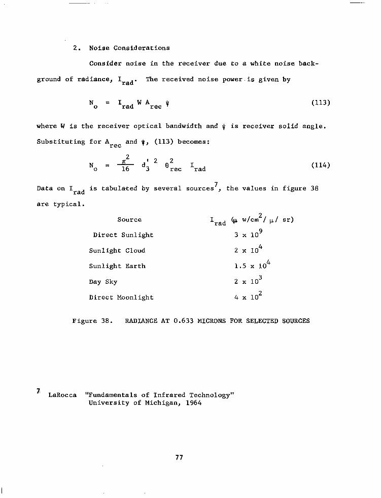
2. Noise Considerations
Consider noise in the receiver due to a white noise back-
ground of radiance, Irad. The received noise power. is given by
No = 'rad ' Arec q (113)
where W is the receiver optical bandwidth and $ is receiver solid angle.
Substituting for Arec and $, (113) becomes:
n2 '2 N =yd3 ‘fkzc ‘rad 0 (114)
Data on Irad 7 is tabulated by several sources , the values in figure 38
are typical.
Source I rad tp w/cm2/ CL/ sr)
Direct Sunlight 3 x log
Sunlight Cloud 2 x lo4
Sunlight Earth 1.5 x lo4
Day Sky 2 x lo3
Direct Moonlight 4 x lo2
Figure 38. RADIANCE AT 0.633 MICRONS FOR SELECTED SOURCES
7: LaRocca "Fundamentals of Infrared Technology" University of Michigan, 1964
77
As a worst case example, consider the breadboard system working against
a sunlit earth background: NL = 2.68 x 10-l' watts. The additive
background noise is attenuated by the receiver optics losses, so the
signal-to-noise ratio may be calculated using the numbers in Figure 36,
assuming no atmospheric attenuation. At 5 kilometers for example:
( + )background = P;zz = 1.67 x lo2 = 22 db. 1
NO
This becomes 15.5 db for 3 kilometer air. It is apparent that the
breadboard system is not background noise limited.
Performance of the photomultiplier involves three sources
of noise: noise due to the dark emission current of the photocathode,
noise due to the average signal photocurrent, and thermal noise generated
in the load resistance. The expression for the ratio of signal current
to tube dark current is8
where
(tli = ik d
c 2e id (1 + -& B)]1'2
ik is the average signal cathode photo current
e is the electronic charge, 1.6 x 10 -19 coulombs.
(115)
id is the tube dark current
m is the secondary emission ratio per stage, M 4
G is a statistical factor = 1.54
B is the receiver bandwidth
8 "Phototubes and Photocells" RCA Technical Manual PT-60, Lancaster, Pa. 1963, pp. 55 ff.
78

The expression for the ratio of signal current to noise in signal current
(shot noise) is similar with i d replaced by ik, Therefore:
ik 112 ( i) =[
ik 2 e(l + 1
(116)
Note that the signal to the shot noise ratio varies directly as the
square root of the average signal current whereas the signal to dark
current ratio is proportional to the average signal current directly.
For ik > id , ( N s, ik is the smaller quantity. In the experimental
model this condition applies and shot noise is the predominant noise
source. For the optimum value of tube lead resistance, the rms Johnson
noise voltage is equal to the dark current noise voltage. Therefore
thermal noise may be ignored with respect to shot noise also.
The average photocathode signal current is
ret ik =' Prec T @ (117)
where T is the transmission factor of the receiver optics and @ is the
cathode sensitivity. The S-20 photocathode has a radiant sensitivitiy
of 2.3 x 10 -2 amp/watt at 0.633 microns. Bandwidth of the RMP-1 con-
verter input stage is 70 MHz. From an earlier discussion T = 0.4
( ~ >i is given in Figure 39 for several ranges using values of k
P ret ret from Figure 36. This is the signal to noise ratio at the optical
detector.
79

.1111. ,111 II ,111 111111.m--~m m ..I_... -. --.....---.-.---_.__. . . .11.1- . . I--.m..----..--q ,..... . ,, .,. . , , m
Range Meters
lo3
2 x lo3
3 x lo3
4 x lo3
5 x lo3
CS N )ik (db)
12.4
9.4
7.6
6.4
5.4
Figure 39. DETECTOR NOISE LIMITED S/N AS A FUNCTION OF RANGE
These S/N ratios are considerably smaller than the worst case background
(S/N) = 22 db; demonstrating that the breadboard system is detector
noise limited.
C. Experimental Data
1. Servo Noise
The Model 119 lasers are locked to the Lamb dip region
of the mode pattern by a servo system. A 5 KHz modulation is applied
to the piezoelectric mirror mount that causes amplitude modulation of
the laser output depending upon the shape of the mode pattern at the
operating point. This AM'ing of the beam is detected by a photocell,
amplified and compared in a phase comparator with the modulating wave-
form. An error signal isgenerated and applied to the mirror to correct
for mirror drift.
80

A noise spectrum is generated in the receiver output of the
breadboard model due to the servo noise. The mirror motion causes FM'ing
of the beam as well as the amplitude modulation. The differnce frequency
contains the beat of the two servo noise spectra. There are line
spectra at 5, 10 and 15 KHz. The noise spectrum peaks below 1 KHz.
This noise prevents use of baseband modulation with the lasers in the
servo lock position. Experience has shown that after 4 to 6 hours
operation the lasers stabilize and servo lock operation is not required
to keep the difference frequency within the bandpass of the receiver.
2. Subcarrier Modulation
The system was operated over a 300 meter link to demonstrate
qualitatively system performance. Subcarrier modulation at 2-4 MHz is
detected with excellent signal to noise when the lasers are stabilized.
Narrow band filters are used to reduce receiver bandwidth. Drive
voltage on the modulator crystal is nominally 150 volts. No quantita-
tive measurements of system performance were made during this phase of
the contract.
3. Video Modulation
In the case of video modulation signal quality is very
poor. Frequency stability of the laser beat was not adequate for
optimum tuning of the receiver in the unlocked servo condition. In
the servo lock condition the noise spreads the difference frequency
spectrum over 20 MHz at a low frequency rate so that signal is lost at
81
the fixed tuned receiver. Performance will be measurably improved by
reducing servo noise and incorporating a tracking local oscillator in
the receiver. These improvements will permit quantitative evaluation
of breadboard model performance.
82 NASA-Langley, 1967