follow the leader architecture 6th order elliptic bandpass …s-sanchez/622follow-the-leader...
TRANSCRIPT

Follow The Leader Architecture
6th Order Elliptic Bandpass Filter
A numerical example
ECE 622(ESS)
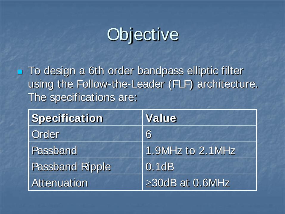
Objective
To design a 6th order bandpass elliptic filter using the Follow-the-Leader (FLF) architecture. The specifications are:
Specification Value Order 6 Passband 1.9MHz to 2.1MHz Passband Ripple 0.1dB Attenuation ≥30dB at 0.6MHz

Realization of High Order Transfer Functions (N>2)
Cascade of 2nd order sections (one 1st order section if N is odd)
Leapfrog Follow-The-Leader
Cascade FLF Leap-Frog
Sensitivity High Medium Low
Easy to Tune Medium Easy Difficult

Primary Resonator Block
It provides compensatory internal interactions between the different filter sections through coupling the biquad building blocks.
Vout
BP1
BP2
BP3
+
-F2
-F3
Vin

Design Questions:
How do we obtain the feedback coefficients F2 and F3?
How do we determine the specifications for each biquadratic section?
Q ωo Gain

Design Procedure
Start with the Lowpass equivalent sytem.
+
-F2
-F3
Vout Vin
K0 kskK+1 ks
kK+2 ks
kK+3
Bad News: Elliptic Filters need finite zeros in their lowpass equivalent transfer function.

Implementation of Finite Zeros by the Summation Technique
+
-F2
-F3
+
B0 B1 B2 B3
Vout
Vin K0 ks
kK+1 ks
kK+2 ks
kK+3
V0 V1 V2 V3

Design Procedure
Let for now K1=K2=K3=1
and (1)
Applying Mason’s rule, the complete transfer function is given by: (2)
ksksT+
=)(
)()(1)()()(
)()()( 3
32
2
33
2210
0 sTFsTFsTBsTBsTBBK
sVsVsH
in
out
+++++
==
( ) ( ) ( )( ) ( ) 3
32
23
33
22
21
30
0 kFkskFkskBkskBkskBksBK
++++++++++
=

Design Procedure From Matlab or Fiesta, we can obtain the lowpass prototype transfer function
of the desired 6th Order Elliptic Filter:
(3)
Equating the denominators of equations (2) and (3), we obtain the following set of equations from which we can solve for k, F2, and F3.
(4)
Also from equations (2) and (3)
(5)
012
23
012
23
3
0
0)(asasasbsbsbsb
bamsH
++++++
=
( ) 03
32
12
22
2
1
3
3
akFF
akFk
ak
=++
=+
=
0
00 b
amK =

Design Procedure
To obtain the summation coefficients, we equate the numerators of equations (2) and (3). If H(s) is a bandpass: B0=b3=0. Then, we obtain the following set of equations from which we can determine B1, B2 and B3.
(6)
( ) 03
321
12
21
21
30
2
0
bkBBB
bkBkB
bkBbB
=++
=+
===

Designing for Maximum Dynamic Range
We need to distribute the gains of each section T(s), i.e. K1, K2 and K3 such that we maximize the Dynamic Range.
The maximum dynamic range will be obtained if the signal spectra at the output of all sections have equal maxima, i.e.
Vout,max=V3,max=V2,max=V1,max=V0,max

Maximizing Dynamic Range To make V3,max= Vout,max
(7)
where
(8) We also need to adjust the summation coefficients to keep the overall gain:
(9)
If we assume a flat spectrum for the input, i.e. Vin(ω)=1 (10)
qKKK 000 =′→
scalingtopriorscalingtoprior
VV
q out
←←
=max,3
max,
qBBB i
ii =′→
)(max, ωHMaxVout =
)(3max,3 ωHMaxV =

Maximizing Dynamic Range
Where
(11) To obtain K1, K2 and K3 :
(12)
012
23
3
03
3 )()()(
asasaskK
sVsVsH
in +++==
.3,2,1
)(
)(
23
2
22
3
24
2
22
3
=
+
+
=−
−
iforkHMax
kHMax
Ki
i
i
ωωω
ωωω

Design Procedure The feedback coefficients need to be readjusted to keep the same loop
gains:
(13)
The summation coefficients also need to be readjusted again:
(14)
21
222 KK
FFF =′→
321
333 KKK
FFF =′→
qBBB
qKBBB
qKKBBB
1333
3222
32111
=′→
=′→
=′→

Summary of Design Procedure Obtain from Matlab or Fiesta the lowpass prototype for the desired filter. From equations (4), (5) and (6), obtain K0, the feedback and the summation
coefficients. To maximize dynamic range, obtain q using equation (8). Recalculate K0
using equation (7). Calculate the gain of each section, i.e. K1, K2 and K3 using equation (12). Recalculate the feedback and summation coefficients using equations (13)
and (14). Finally, apply a lowpass-to-bandpass transformation to obtain the desired
bandpass filter specifications:
where Q is the quality factor of the overall filter and Q0 is that required for each biquad section.
Note: A Matlab program was written to automate the design procedure for an arbitrary filter specification of order N.
kQQ
ff UL
=
=
0
0 2πω

Summary of Results For the required specifications, the following values
were obtained: Feedback Coefficients F2 = 0.657640
F3 = 0.227545
Feedforward Coefficients B0 = 0 B1 = 0.169792 B2 = -0.216571 B3 = 1.129814
Gain for the input and each biquad stage
K0 = 0.604488 K1 = 2.349 K2 = 2.165 K3 = 2
Center frequency and Q0 of each biquad stage
f0 = 1.9975MHz Q0 = 15.7

Simulation Results System Level
The complete filter was simulated in Cadence at a system-level. The results are shown below:
Magnitude Response Phase Response
Ripple ≤ 0.1dB

Transistor Level Implementation
To implement each biquadratic section, a two-integrator loop biquad OTA-C filter was used.
Advantages with respect to Active-RC: Easy Tunability by changing the bias currents of the OTAs.
(Active-RC needs the use of varactors). Lower Power Consumption and Smaller Area.
Disadvantages with respect to Active-RC:
Smaller Dynamic Range Poorer Linearity

Transistor Level Implementation of each Biquad Section
Vout
Vin gm1+
-
OUT
gm4
+
-
OUT
gm2+
-
OUT
gm3
+
-
OUTC1
C2
R
R
12
32
1
42
1
1
)(
CCgg
Cgss
Cgs
sHmmm
m
++=

Design of Lossless Integrator The lossless integrator was designed to have unity gain at
f0=1.9975MHz.
The following specifications are needed if a 5% variation in Q is allowed:
This image cannot currently be displayed.
1)(2
2 ==C
gH m
ωω
VAgm µ52.3763 =
pFC 302 =
°=×=
−≤ − 086.0105.11
21: 3 rad
QPhaseExcess
aEφ
dB
QAGainDC
a
V 58.556021
2: ==−
≥

Design of Lossless Integrator Due to the relatively high DC gain required for the OTA, a folded-
cascode topology was used:
VSS
VDD
M1 M2
M3 M4 M5
M6 M7
M8M9
M10 M11
M12 M13
Ibias
M14
Vin+Vout
Vin-
Vbp
Vbn
Transconductance DC Gain GBW Bias Current Power Consumption Active Area
376.52µA/V 64.1dB 263MHz 40µA 792µW 727µm2

Simulation Results of the Lossless Integrator
The excess phase without any compensation was 1.17°. Passive excess phase compensation was used →R=55Ω.
Magnitude Response Phase Response

Design of Biquadratic Bandpass Filter
To reuse the designed OTA:
Transconductance gm1 depends on Ki
For demonstrations purposes, gm1=gm4, i.e. K=1
VAgg mm µ52.37623 ==
pFCC 3021 ==
VAQCgm µω 827.230
0
14 ==
41 mim gKg =

Design of Biquadratic Bandpass Filter
Due to the relatively small transconductance required, source degeneration was used. Also, a PMOS differential pair was more suitable.
Transconductance DC Gain GBW Bias Current Power Consumption Active Area
23.827µA/V 61.15dB 62.3MHz 14µA 277.2µW 820µm2
VSS
VDD
M9 M8
M11M10
M13M12
R
M14
Ibias
M1 M2
M3A M3BM4 M5
M7M6
VoutVin+ Vin-
Vbp
Vbn

Simulation Results of the Biquadratic Bandpass Filter
Frequency Response Step Response

Summation Nodes To complete the transistor-level design, we need two
summation nodes:
+
-F2
-F3
+
B0 B1 B2 B3
Vout
Vin K0 ks
kK+1 ks
kK+2 ks
kK+3
V0 V1 V2 V3

Summation Nodes
Vin
V2
V3
V0
K0 gm0+
-
OUT
F2 gm0
+
-
OUT
F3 gm0
+
-
OUTgm0
+
-
OUT
V2
Vout
V1
V3
gm0
+
-
OUT
B3 gm0+
-
OUT
B2 gm0
+
-
OUT
B1 gm0+
-
OUT
The summation nodes can be implemented with OTAs in the following configurations:
Summation Node for the Feedback Paths Summation Node at the Output
If gm0 is chosen large enough, the output resistance of each OTA does not need to be very high. Excess Phase of OTAs can be a concern.

Summation Nodes Due to the desired low excess phase introduced by the OTAs, it is
more convenient to use a simple differential pair.
Transconductance Bias Current Power Consumption Active Area
300µA/V 40µA 264µW 269µm2
VDD
VSS
M2
M12
M1
M13
M3
Ibias
M9
Vin-
Vout
Vin+

Simulation Results of the Complete FLF Filter (Transistor vs. System Level)
Magnitude Response Phase Response
Ripple ~0.2dB

Simulation Results of the Complete FLF Filter (Transistor vs. System Level)
Transient Response to a Sinewave Step Response

Summary of Results
Specification Value
Passband 1.9MHz to 2.1MHz
Passband Ripple ~0.2dB
Attenuation ≥40dB at 0.6MHz
Power Consumption 8.53mW
Active Area 11,434µm2
Total Area ~ 211,549µm2

Problems to be solved
Voltage Swing: The allowable input voltage swing is only 100mV. A small voltage swing is expected, since the OTAs have a small linear range limited by ±VDSAT of the input transistors (in case no linearization technique is used, such as source degeneration or others). Nevertheless, 100mV is too small and is basically because the OTAs with gm=376.52µA/V use input transistors with a small VDSAT and no linearization technique is being used. I need to redesign these OTAs to increase the linear range.
Bias Network: To design the bias network for the folded-cascode OTAs capable of effectively tracking changes of VT due to process variations.
Sensitivity and Tunability: To characterize the complete filter in terms of sensitivity and tunability.
Layout

References
[1] Sedra, Brackett. Filter Theory and Design: Active and Passive. Matrix Series in Circuits and Systems. pp. 589-659.
[2] Deliyannis, Sun, Fidler. Continuous-Time Active Filter Design. CRC Press
1999. pp. 151-180. [3] G. Hurtig, III. The Primary Resonator Block Technique of Filter Synthesis
Proc. Int. Filter Symposium, p.84, 1972. [4] Barbargires. Explicit Design of General High-Order FLF OTA-C Filters.
Electronics Letters. 5th August 1999, Vol. 35, No. 16, pp. 1289-1290. [5] Jie Wu, Ezz I. El-Masry. Synthesis of Follow-the-Leader Feedback Log-
Domain Filters. IEEE 1998. 0-7803-5008-1/98. pp. 381-384.