formike electronic co.,ltd - display future · formike electronic co.,ltd address :room a818 new...
TRANSCRIPT
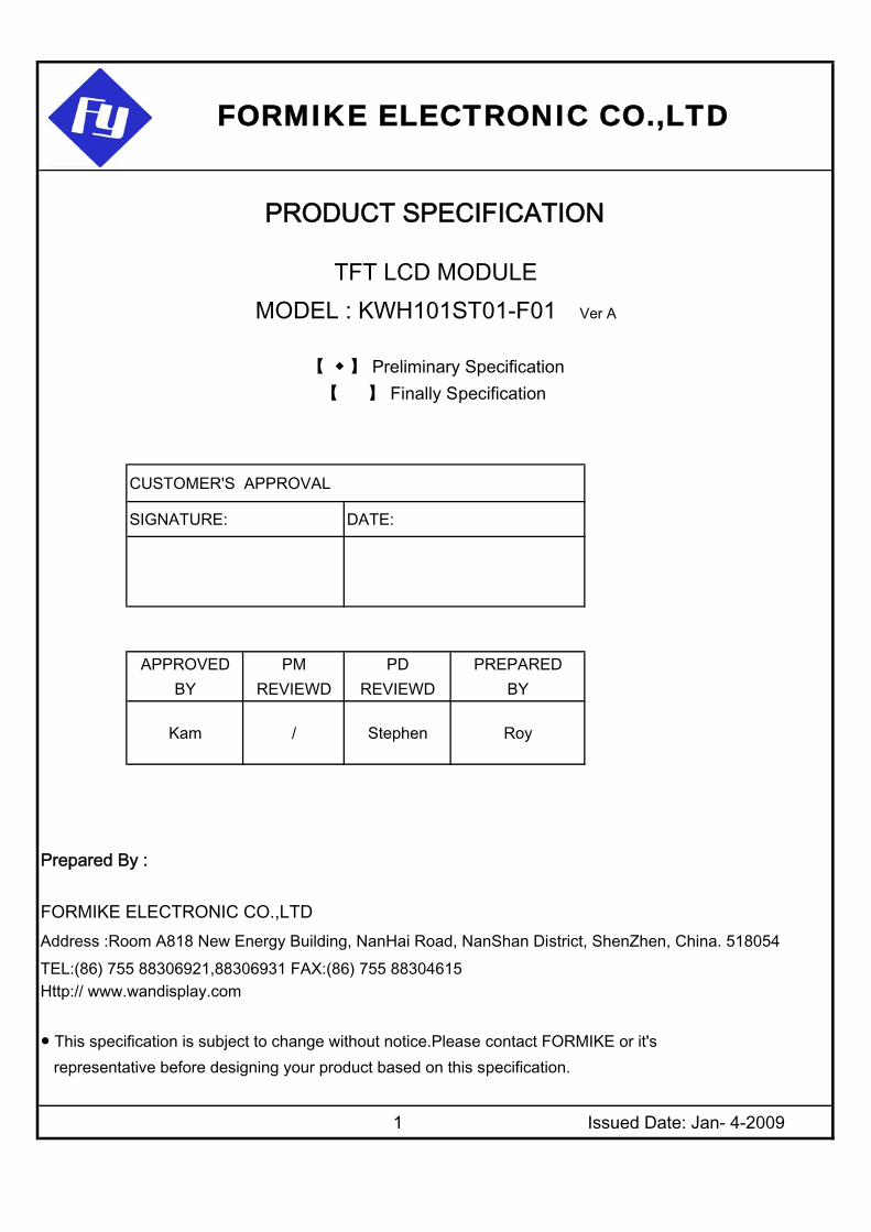
【 】 Finally Specification
CUSTOMER'S APPROVAL
SIGNATURE: DATE:
APPROVED PM PD PREPAREDBY REVIEWD REVIEWD BY
Kam / Stephen Roy
Prepared By :
FORMIKE ELECTRONIC CO.,LTD Address :Room A818 New Energy Building, NanHai Road, NanShan District, ShenZhen, China. 518054
TEL:(86) 755 88306921,88306931 FAX:(86) 755 88304615 Http:// www.wandisplay.com
● This specification is subject to change without notice.Please contact FORMIKE or it's representative before designing your product based on this specification.
1 Issued Date: Jan- 4-2009
【 ◆ 】 Preliminary Specification
FORMIKE ELECTRONIC CO.,LTD
PRODUCT SPECIFICATION
TFT LCD MODULEMODEL : KWH101ST01-F01 Ver A
、 、
FORMIKE ELECTRONIC CO.,LTD Module No.: KWH101ST01-F01
CONTENTS 1. GENERAL DESCRIPTION -------------------------------------------------------------------------------------------3 1.1 OVERVIEW----------------------------------------------------------------------------------------------------------------------------3 1.2 FEATURES----------------------------------------------------------------------------------------------------------------------------3 1.3 APPLICATION------------------------------------------------------------------------------------------------------------------------3 1.4 GENERAL SPECIFICATIONS----------------------------------------------------------------------------------------------------3 1.5 MECHANICAL SPECIFICATIONS-----------------------------------------------------------------------------------------------3
2. ABSOLUTE MAXIMUM RATINGS----------------------------------------------------------------------------------4 2.1 ABSOLUTE RATINGS OF ENVIRONMENT---------------------------------------------------------------------------------4 2.2 ELECTRICAL ABSOLUTE RATINGS -----------------------------------------------------------------------------------------5
2.2.1 TFT LCD MODULE5 ---------------------------------------------------------------------------------------------------------5 2.2.2 BACKLIGHT UNIT5 ----------------------------------------------------------------------------------------------------------5
3. ELECTRICAL CHARACTERISTICS -------------------------------------------------------------------------------6 3.1 TFT LCD MODULE-------------------------------------------------------------------------------------------------------------------7 3.2 BACKLIGHT UNIT -------------------------------------------------------------------------------------------------------------------8
4. BLOCK DIAGRAM -------------------------------------------------------------------------------------------------------9 4.1 TFT LCD MODULE ------------------------------------------------------------------------------------------------------------------9
5. INPUT TERMINAL PIN ASSIGNMENT ---------------------------------------------------------------------------10 5.1 TFT LCD MODULE -----------------------------------------------------------------------------------------------------------------11 5.2 TIMING DIAGRAM OF LVDS INPUT SIGNAL-------------------------------------------------------------------------------11 5.3 COLOR DATA INPUT ASSIGNMENT -----------------------------------------------------------------------------------------12
6. CONVERTER SPECIFICATION-------------------------------------------------------------------------------------15 6.1 ABSOLUTE MAXIMUM RATINGS ----------------------------------------------------------------------------------------------15 6.2 RECOMMENDED OPERATING RATINGS ----------------------------------------------------------------------------------15 6.3 LED BACKLIGHT CONTROLL ON/OFF SEQUENCE ----------------------------------------------------------15
7. INTERFACE TIMING----------------------------------------------------------------------------------------------------16 7.1 INPUT SIGNAL TIMING SPECIFICATIONS-----------------------------------------------------------------------------------16 7.2 POWER ON/OFF SEQUENCE----------------------------------------------------------------------------------------------------16
8. OPTICAL CHARACTERISTICS --------------------------------------------------------------------------------------17 8.1 TEST CONDITIONS -----------------------------------------------------------------------------------------------------------------17 8.2 OPTICAL SPECIFICATIONS-------------------------------------------------------------------------------------------------------18
9. PRECAUTIONS-------------------------------------------------------------------------------------------------------------19 9.1 SYSTEM MATCHING PRECAUTIONS-------------------------------------------------------------------------------------------19 9.2 HANDLING PRECAUTIONS---------------------------------------------------------------------------------------------------------19 9.3 STORAGE PRECAUTIONS----------------------------------------------------------------------------------------------------------199.4 OPERATION PRECAUTIONS-------------------------------------------------------------------------------------------------------199.5 OTHER PRECAUTIONS -------------------------------------------------------------------------------------------------------------19
10. PACKING ------------------------------------------------------------------------------------------------------------------20
2
1. GENERAL DESCRIPTION 1.1 OVERVIEW
is a 10.1” TFT Liquid Crystal Display module with LED Backlight unit and 40 pins LVDS
interface. This module supports 1024 x 600 Wide-SVGA mode and can display 262,144 colors. The
optimum viewing angle is at 6 o’clock direction. The converter module for Backlight is built in.
1.2 FEATURES
- WSVGA (1024 x 600 pixels) resolution
- 3.3V LVDS (Low Voltage Differential Signaling) interface with 1 pixel/clock
- Build in LED Converter
1.3 APPLICATION
- TFT LCD Notebook
1.4 GENERAL SPECIFICATI0NS Item Specification Unit Note
Active Area 222.72 (H) x 125.28 (V) (10.06” diagonal) mm Bezel Opening Area 226.34 (H) x 128.1 (V) mm
(1)
Driver Element a-si TFT active matrix - - Pixel Number 1024 x R.G.B. x 600 pixel - Pixel Pitch 0.2175 (H) x 0.2088 (V) mm - Pixel Arrangement RGB vertical stripe - - Display Colors 262,144 color - Transmissive Mode Normally white - - Surface Treatment Hard coating (3H), Glare - -
1.5 MECHANICAL SPECIFICATIONS Item Min. Typ. Max. Unit Note
Horizontal(H) 234.5 235.0 235.5 mm Vertical(V) 142.5 143.0 143.5 mm Module Size Thickness(T) - 4.9 5.2 mm
(1)
Weight - 180 190 g
Note (1) Please refer to the attached drawings for more information of front and back outline dimensions.
FORMIKE ELECTRONIC CO.,LTD Module No.: KWH101ST01-F01
KWH101ST01
3

2. ABSOLUTE MAXIMUM RATINGS 2.1 ABSOLUTE RATINGS OF ENVIRONMENT
Value Item Symbol Min. Max. Unit Note
Storage Temperature TST -20 +60 ºC (1) Operating Ambient Temperature TOP 0 +50 ºC (1), (2) Shock (Non-Operating) SNOP - 220/2 G/ms (3), (5) Vibration (Non-Operating) VNOP - 1.5 G (4), (5)
Note (1) Temperature and relative humidity range is shown in the figure below.
(a) 90 %RH Max. (Ta <= 40 ºC).
(b) Wet-bulb temperature should be 39 ºC Max. (Ta > 40 ºC).
(c) No condensation.
Note (2) The temperature of panel surface area should be 0 ºC min. and 60 ºC max.
Note (3) 1 time for ± X, ± Y, ± Z. for Condition (220G / 2ms) is half Sine Wave,.
Note (4) 10~500 Hz, 30 min/cycle, 1cycle for X,Y,Z-axis.
Note (5) At testing Vibration and Shock, the fixture in holding the module has to be hard and rigid
enough so that the module would not be twisted or bent by the fixture.
The fixing condition is shown as below:
Side Mount Fixing Screw Side Mount Fixing Screw
Stage
Bracket
LCD Module
Gap=2mm
At Room Temperature
Storage Range
Relative Humidity (%RH)
Operating Range
Temperature (ºC)
100
80 60 -20 40 0 20 -40
80
40
60
20 10
90
FORMIKE ELECTRONIC CO.,LTD Module No.: KWH101ST01-F01
4
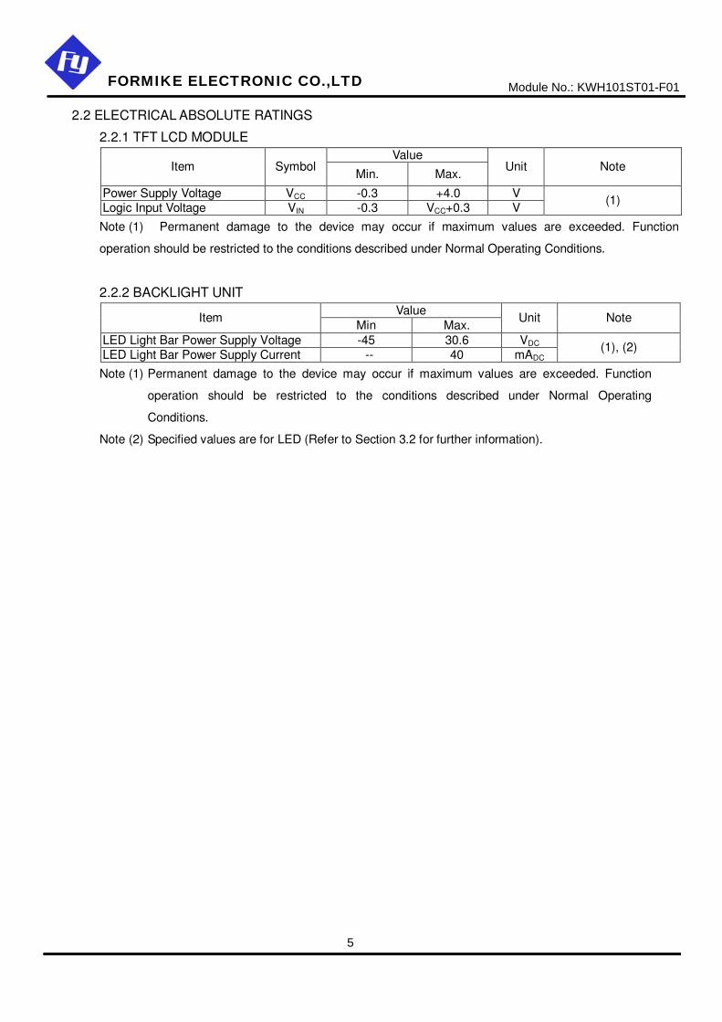
2.2 ELECTRICAL ABSOLUTE RATINGS
2.2.1 TFT LCD MODULE Value
Item Symbol Min. Max.
Unit Note
Power Supply Voltage VCC -0.3 +4.0 V Logic Input Voltage VIN -0.3 VCC+0.3 V
(1)
Note (1) Permanent damage to the device may occur if maximum values are exceeded. Function
operation should be restricted to the conditions described under Normal Operating Conditions.
2.2.2 BACKLIGHT UNIT Value Item
Min Max. Unit Note
LED Light Bar Power Supply Voltage -45 30.6 VDC LED Light Bar Power Supply Current -- 40 mADC
(1), (2)
Note (1) Permanent damage to the device may occur if maximum values are exceeded. Function
operation should be restricted to the conditions described under Normal Operating
Conditions.
Note (2) Specified values are for LED (Refer to Section 3.2 for further information).
FORMIKE ELECTRONIC CO.,LTD Module No.: KWH101ST01-F01
5
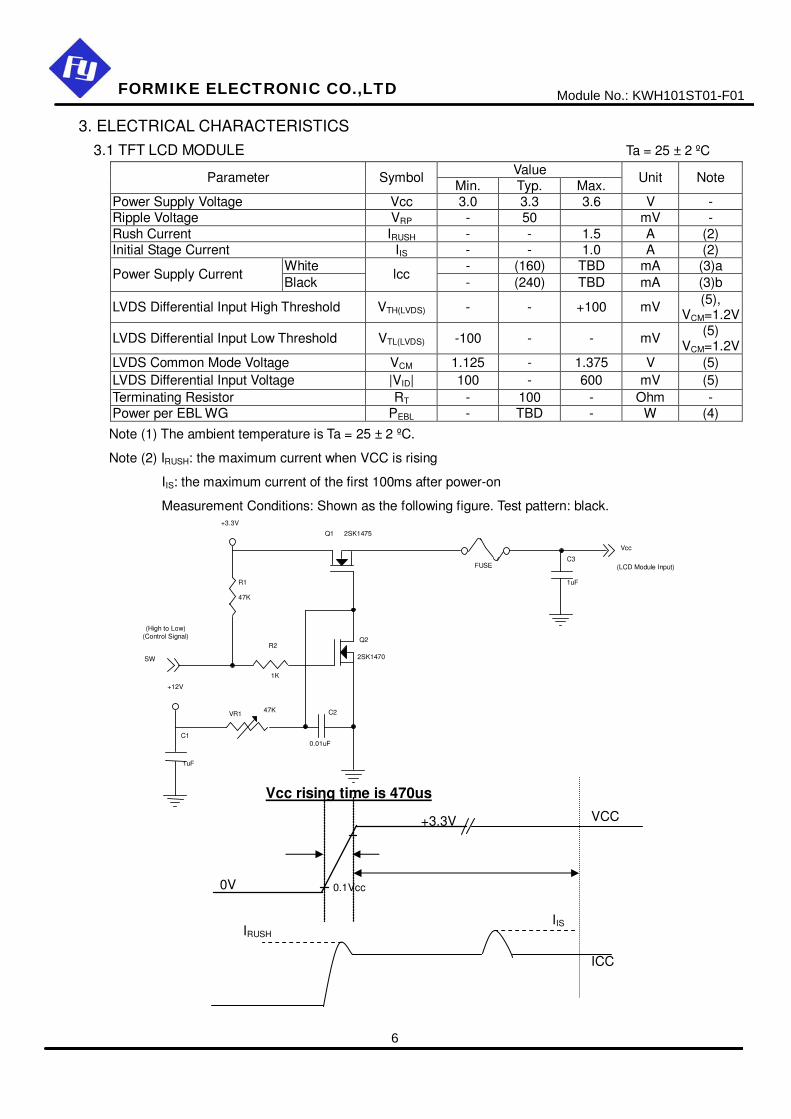
3. ELECTRICAL CHARACTERISTICS 3.1 TFT LCD MODULE Ta = 25 ± 2 ºC
Value Parameter Symbol Min. Typ. Max.
Unit Note
Power Supply Voltage Vcc 3.0 3.3 3.6 V - Ripple Voltage VRP - 50 mV - Rush Current IRUSH - - 1.5 A (2) Initial Stage Current IIS - - 1.0 A (2)
White - (160) TBD mA (3)a Power Supply Current
Black lcc
- (240) TBD mA (3)b
LVDS Differential Input High Threshold VTH(LVDS) - - +100 mV (5), VCM=1.2V
LVDS Differential Input Low Threshold VTL(LVDS) -100 - - mV (5) VCM=1.2V
LVDS Common Mode Voltage VCM 1.125 - 1.375 V (5) LVDS Differential Input Voltage |VID| 100 - 600 mV (5) Terminating Resistor RT - 100 - Ohm - Power per EBL WG PEBL - TBD - W (4)
Note (1) The ambient temperature is Ta = 25 ± 2 ºC.
Note (2) IRUSH: the maximum current when VCC is rising
IIS: the maximum current of the first 100ms after power-on
Measurement Conditions: Shown as the following figure. Test pattern: black.
R1
(High to Low) (Control Signal)
+12V
SW Q2
C1
1uF
Vcc
+3.3V
2SK1470
Q1 2SK1475
47K
R2
1K
VR1 47K C2
0.01uF
C3 1uF
FUSE (LCD Module Input)
Vcc rising time is 470us
+3.3V
0V 0.1Vcc
VCC
IIS
ICC
IRUSH
FORMIKE ELECTRONIC CO.,LTD Module No.: KWH101ST01-F01
6
Note (3) The specified power supply current is under the conditions at Vcc = 3.3 V, Ta = 25 ± 2 ºC, DC
Current and fv = 60 Hz, whereas a power dissipation check pattern below is displayed.
Note (4) The specified power are the sum of LCD panel electronics input power and the inverter input
power. Test conditions are as follows.
(a) Vcc = 3.3 V, Ta = 25 ± 2 ºC, fv = 60 Hz,
(b) The pattern used is a black and white 32 x 36 checkerboard, slide #100 from the VESA file
“Flat Panel Display Monitor Setup Patterns”, FPDMSU.ppt.
(c) Luminance: 60 nits.
Note (5) The parameters of LVDS signals are defined as the following figures.
Active Area
a. White Pattern
Active Area
b. Black Pattern
0V
VCM |VID|
Single Ended
0V
|VID| VTH(LVDS)
VTL(LVDS)
Differential
FORMIKE ELECTRONIC CO.,LTD Module No.: KWH101ST01-F01
7
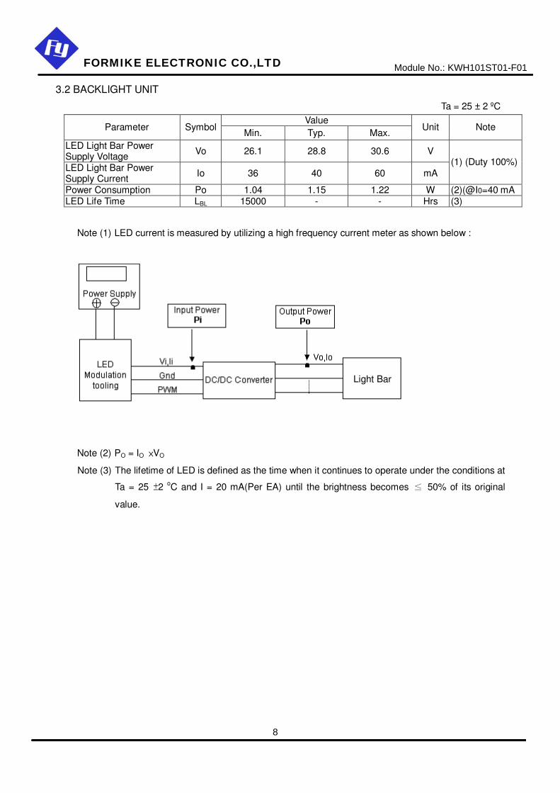
3.2 BACKLIGHT UNIT
Ta = 25 ± 2 ºC Value
Parameter Symbol Min. Typ. Max. Unit Note
LED Light Bar Power Supply Voltage Vo 26.1 28.8 30.6 V
LED Light Bar Power Supply Current Io 36 40 60 mA
(1) (Duty 100%)
Power Consumption Po 1.04 1.15 1.22 W (2)(@I0=40 mA LED Life Time LBL 15000 - - Hrs (3)
Note (1) LED current is measured by utilizing a high frequency current meter as shown below :
Note (2) PO = IO �VO
Note (3) The lifetime of LED is defined as the time when it continues to operate under the conditions at
Ta = 25 �2 oC and I = 20 mA(Per EA) until the brightness becomes � 50% of its original
value.
Light Bar
FORMIKE ELECTRONIC CO.,LTD Module No.: KWH101ST01-F01
8
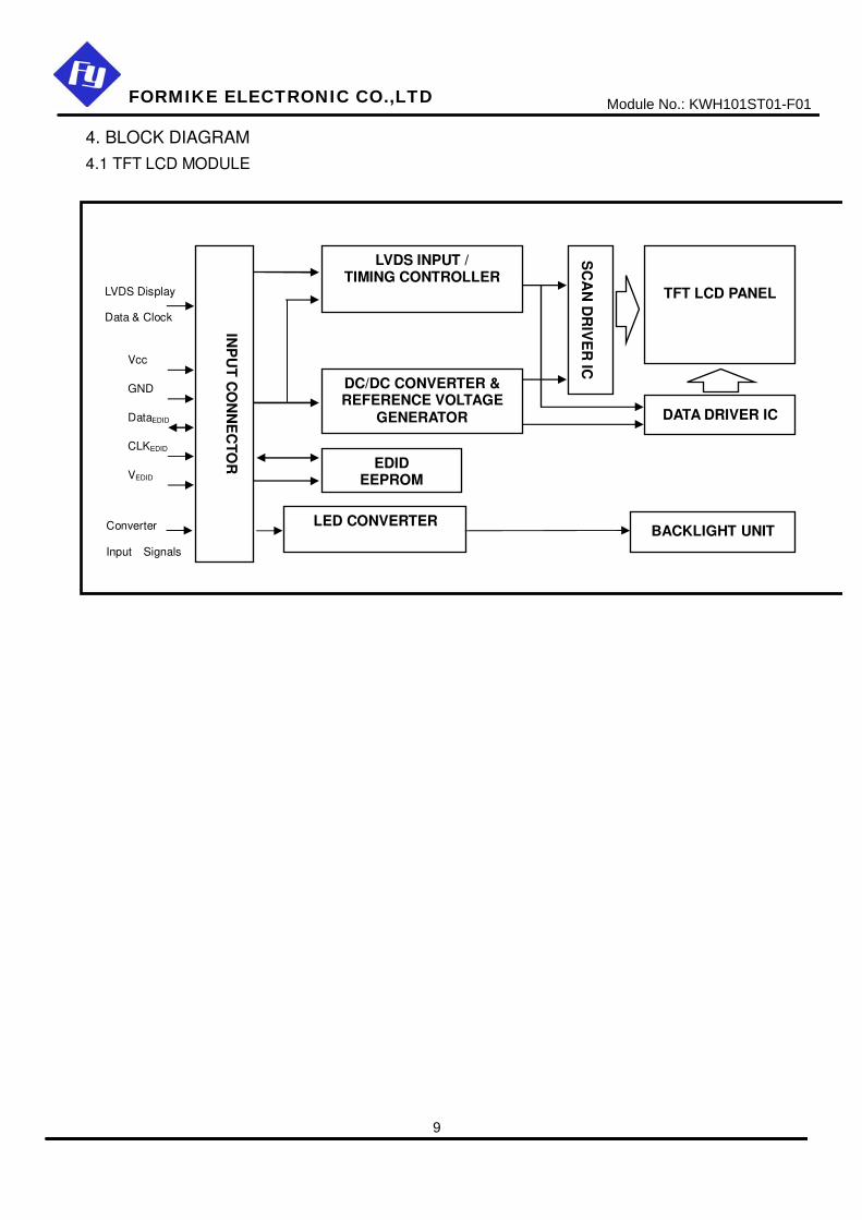
4. BLOCK DIAGRAM 4.1 TFT LCD MODULE
VEDID
DataEDID
Vcc
GND
Converter
Input Signals
LVDS Display
Data & Clock
TFT LCD PANEL
DATA DRIVER IC
SC
AN
DR
IVE
R IC
BACKLIGHT UNIT
LVDS INPUT / TIMING CONTROLLER
DC/DC CONVERTER & REFERENCE VOLTAGE
GENERATOR
INP
UT C
ON
NE
CTO
R
LED CONVERTER
EDID EEPROM
CLKEDID
FORMIKE ELECTRONIC CO.,LTD Module No.: KWH101ST01-F01
9
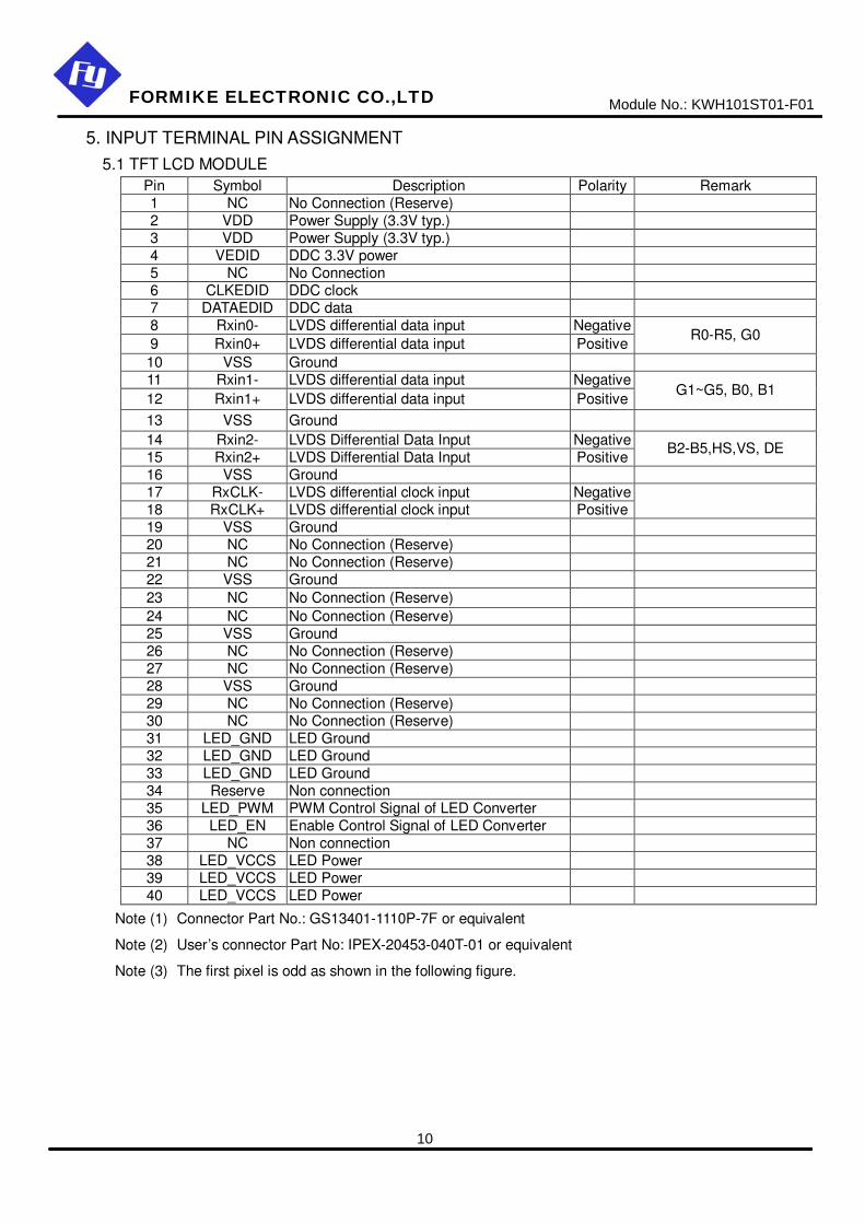
5. INPUT TERMINAL PIN ASSIGNMENT 5.1 TFT LCD MODULE
Pin Symbol Description Polarity Remark 1 NC No Connection (Reserve) 2 VDD Power Supply (3.3V typ.) 3 VDD Power Supply (3.3V typ.) 4 VEDID DDC 3.3V power 5 NC No Connection 6 CLKEDID DDC clock 7 DATAEDID DDC data 8 Rxin0- LVDS differential data input Negative 9 Rxin0+ LVDS differential data input Positive R0-R5, G0
10 VSS Ground 11 Rxin1- LVDS differential data input Negative 12 Rxin1+ LVDS differential data input Positive G1~G5, B0, B1
13 VSS Ground 14 Rxin2- LVDS Differential Data Input Negative 15 Rxin2+ LVDS Differential Data Input Positive B2-B5,HS,VS, DE
16 VSS Ground 17 RxCLK- LVDS differential clock input Negative 18 RxCLK+ LVDS differential clock input Positive
19 VSS Ground 20 NC No Connection (Reserve) 21 NC No Connection (Reserve) 22 VSS Ground 23 NC No Connection (Reserve) 24 NC No Connection (Reserve) 25 VSS Ground 26 NC No Connection (Reserve) 27 NC No Connection (Reserve) 28 VSS Ground 29 NC No Connection (Reserve) 30 NC No Connection (Reserve) 31 LED_GND LED Ground 32 LED_GND LED Ground 33 LED_GND LED Ground 34 Reserve Non connection 35 LED_PWM PWM Control Signal of LED Converter 36 LED_EN Enable Control Signal of LED Converter 37 NC Non connection 38 LED_VCCS LED Power 39 LED_VCCS LED Power 40 LED_VCCS LED Power
Note (1) Connector Part No.: GS13401-1110P-7F or equivalent
Note (2) User’s connector Part No: IPEX-20453-040T-01 or equivalent
Note (3) The first pixel is odd as shown in the following figure.
FORMIKE ELECTRONIC CO.,LTD Module No.: KWH101ST01-F01
10
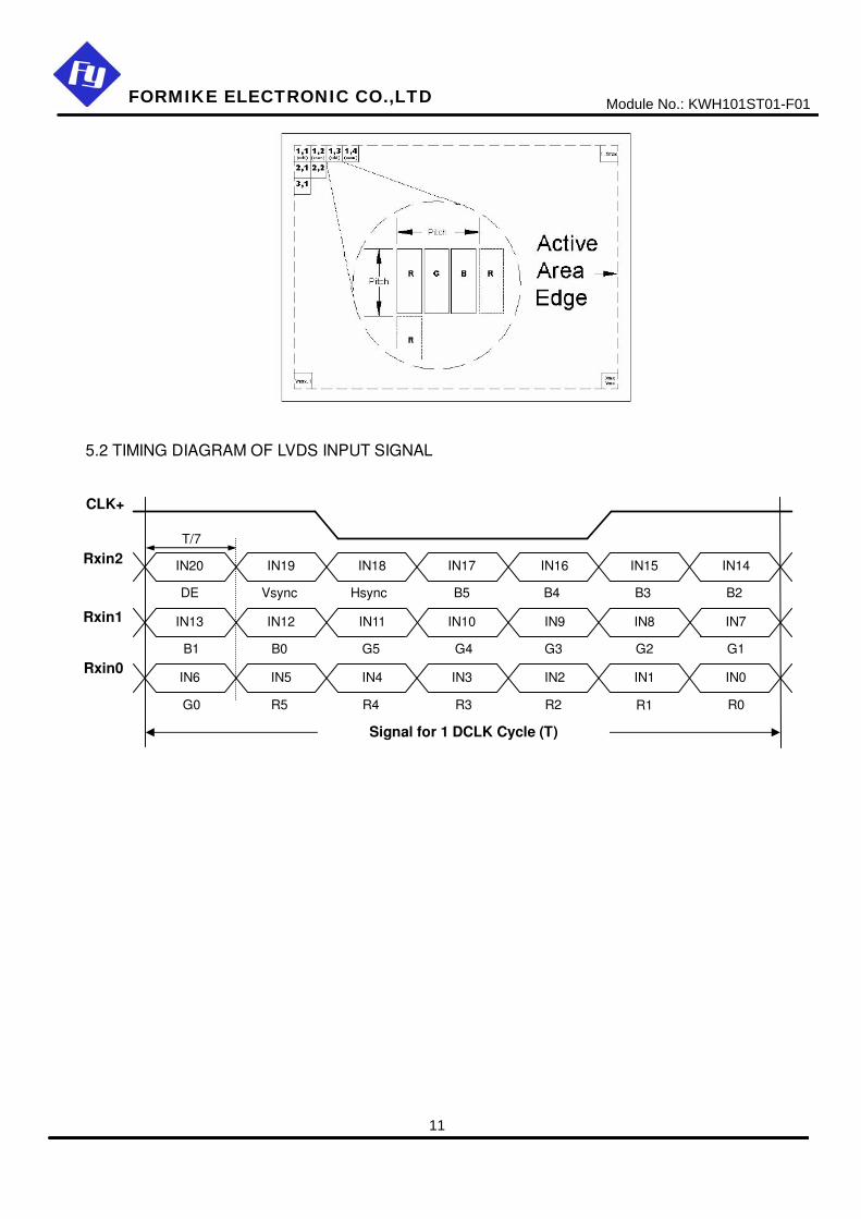
5.2 TIMING DIAGRAM OF LVDS INPUT SIGNAL
T/7
IN6 IN5 IN4 IN3 IN2 IN1 IN0
IN13 IN12 IN11 IN10 IN9 IN8 IN7
IN20 IN19 IN18 IN17 IN16 IN15 IN14
G0 R3 R2 R1 R0 R5 R4
B1 G4 G3 G2 G1 B0 G5
DE B5 B4 B3 B2 Vsync Hsync
Signal for 1 DCLK Cycle (T)
Rxin0
Rxin1
Rxin2
CLK+
FORMIKE ELECTRONIC CO.,LTD Module No.: KWH101ST01-F01
11

5.3 COLOR DATA INPUT ASSIGNMENT
The brightness of each primary color (red, green and blue) is based on the 6-bit gray scale data
input for the color. The higher the binary input the brighter the color. The table below provides the
assignment of color versus data input. Data Signal
Red Green Blue Color R5 R4 R3 R2 R1 R0 G5 G4 G3 G2 G1 G0 B5 B4 B3 B2 B1 B0
Basic Colors
Black Red Green Blue Cyan Magenta Yellow White
0 1 0 0 0 1 1 1
0 1 0 0 0 1 1 1
0 1 0 0 0 1 1 1
0 1 0 0 0 1 1 1
0 1 0 0 0 1 1 1
0 1 0 0 0 1 1 1
0 0 1 0 1 0 1 1
0 0 1 0 1 0 1 1
0 0 1 0 1 0 1 1
0 0 1 0 1 0 1 1
0 0 1 0 1 0 1 1
0 0 1 0 1 0 1 1
0 0 0 1 1 1 0 1
0 0 0 1 1 1 0 1
0 0 0 1 1 1 0 1
0 0 0 1 1 1 0 1
0 0 0 1 1 1 0 1
0 0 0 1 1 1 0 1
Gray Scale Of Red
Red(0)/Dark Red(1) Red(2)
: :
Red(61) Red(62) Red(63)
0 0 0 : : 1 1 1
0 0 0 : : 1 1 1
0 0 0 : : 1 1 1
0 0 0 : : 1 1 1
0 0 1 : : 0 1 1
0 1 0 : : 1 0 1
0 0 0 : : 0 0 0
0 0 0 : : 0 0 0
0 0 0 : : 0 0 0
0 0 0 : : 0 0 0
0 0 0 : : 0 0 0
0 0 0 : : 0 0 0
0 0 0 : : 0 0 0
0 0 0 : : 0 0 0
0 0 0 : : 0 0 0
0 0 0 : : 0 0 0
0 0 0 : : 0 0 0
0 0 0 : : 0 0 0
Gray Scale Of Green
Green(0)/Dark Green(1) Green(2)
: :
Green(61) Green(62) Green(63)
0 0 0 : : 0 0 0
0 0 0 : : 0 0 0
0 0 0 : : 0 0 0
0 0 0 : : 0 0 0
0 0 0 : : 0 0 0
0 0 0 : : 0 0 0
0 0 0 : : 1 1 1
0 0 0 : : 1 1 1
0 0 0 : : 1 1 1
0 0 0 : : 1 1 1
0 0 1 : : 0 1 1
0 1 0 : : 1 0 1
0 0 0 : : 0 0 0
0 0 0 : : 0 0 0
0 0 0 : : 0 0 0
0 0 0 : : 0 0 0
0 0 0 : : 0 0 0
0 0 0 : : 0 0 0
Gray Scale Of Blue
Blue(0)/Dark Blue(1) Blue(2)
: :
Blue(61) Blue(62) Blue(63)
0 0 0 : : 0 0 0
0 0 0 : : 0 0 0
0 0 0 : : 0 0 0
0 0 0 : : 0 0 0
0 0 0 : : 0 0 0
0 0 0 : : 0 0 0
0 0 0 : : 0 0 0
0 0 0 : : 0 0 0
0 0 0 : : 0 0 0
0 0 0 : : 0 0 0
0 0 0 : : 0 0 0
0 0 0 : : 0 0 0
0 0 0 : : 1 1 1
0 0 0 : : 1 1 1
0 0 0 : : 1 1 1
0 0 0 : : 1 1 1
0 0 1 : : 0 1 1
0 1 0 : : 1 0 1
Note (1) 0: Low Level Voltage, 1: High Level Voltage
FORMIKE ELECTRONIC CO.,LTD Module No.: KWH101ST01-F01
12
I
6.CONVERTER SPECIFICATION
6.1 ABSOLUTE MAXIMUM RATINGS Symbol Ratings
LED_VCCS 28.0V
LED_PWM, LED_EN -0.3V~5.5V
6.2 RECOMMENDED OPERATING RATINGS Value Parameter Symbol
Min. Typ. Max. Unit Note
Converter Input power supply voltage LED_Vccs 5 12 20 V Backlight on (2) --- (5) V EN Control Level Backlight off
0 --- (0.8) V
PWM High Level (2) --- (5) V PWM Control Level PWM Low Level
0 --- (0.15) V
PWM Control Duty Ratio (20) 100 % PWM Control Permissive Ripple Voltage VPWM_pp 100 mV PWM Control Frequency fPWM 190 210 230 Hz
LED_VCCS=Min (220) (271) (321) mA (1) LED_VCCS=Typ (92) (113) (134) mA (1) LED Power Current LED_VCCS=Max
IBL (52) (65) (77) mA (1)
Note (1) The specified LED power supply current is under the conditions at “LED_VCCS = Min, Typ,
Max”, Ta = 25 ± 2 ºC, fPWM = 200 Hz, Duty=100%.
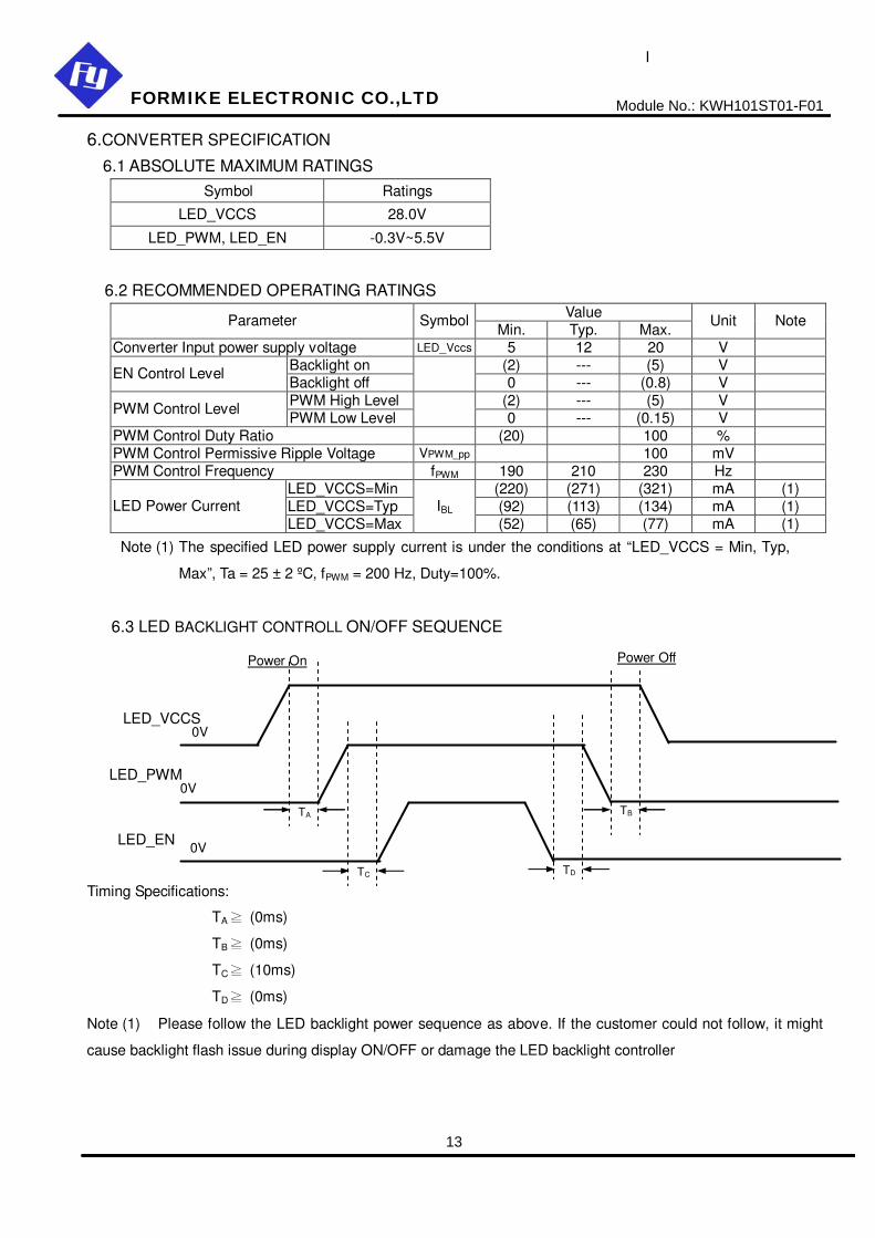
6.3 LED BACKLIGHT CONTROLL ON/OFF SEQUENCE Timing Specifications:
TA � (0ms)
TB � (0ms)
TC � (10ms)
TD � (0ms) Note (1) Please follow the LED backlight power sequence as above. If the customer could not follow, it might
cause backlight flash issue during display ON/OFF or damage the LED backlight controller
TA
LED_VCCS
0V
LED_PWM 0V
LED_EN 0V
TC TD
TB
Power On Power Off
FORMIKE ELECTRONIC CO.,LTD Module No.: KWH101ST01-F01
13
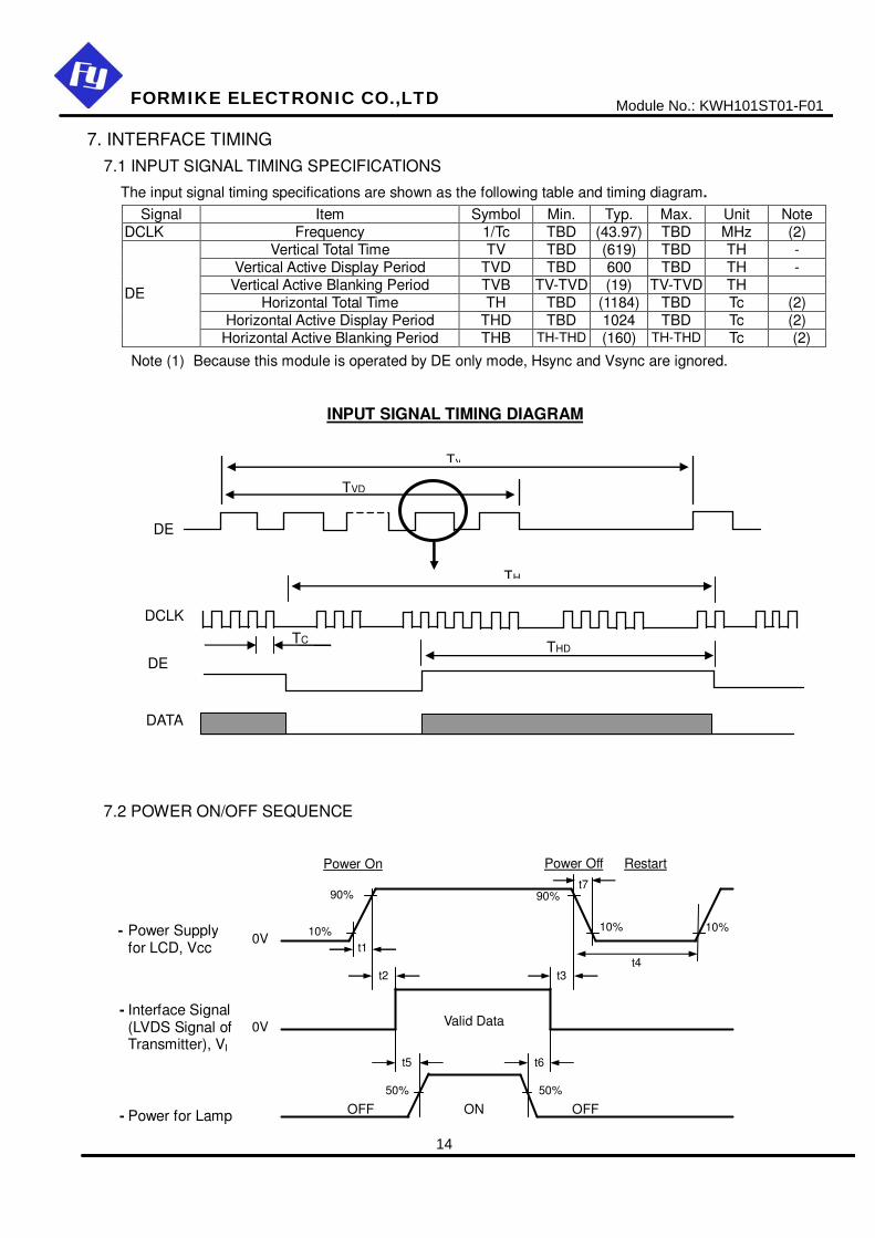
7. INTERFACE TIMING 7.1 INPUT SIGNAL TIMING SPECIFICATIONS
The input signal timing specifications are shown as the following table and timing diagram. Signal Item Symbol Min. Typ. Max. Unit Note
DCLK Frequency 1/Tc TBD (43.97) TBD MHz (2) Vertical Total Time TV TBD (619) TBD TH -
Vertical Active Display Period TVD TBD 600 TBD TH - Vertical Active Blanking Period TVB TV-TVD (19) TV-TVD TH
Horizontal Total Time TH TBD (1184) TBD Tc (2) Horizontal Active Display Period THD TBD 1024 TBD Tc (2)
DE
Horizontal Active Blanking Period THB TH-THD (160) TH-THD Tc (2)
Note (1) Because this module is operated by DE only mode, Hsync and Vsync are ignored.
INPUT SIGNAL TIMING DIAGRAM
7.2 POWER ON/OFF SEQUENCE
TH
TC DCLK
THD
TVD
Tv
DE
DE
DATA
- Power Supply for LCD, Vcc
- Interface Signal (LVDS Signal of Transmitter), VI
- Power for Lamp
Restart Power On Power Off
50% 50%
0V
0V 10%
t6 t5
t4 t3 t2
t1
90%
10%
90%
Valid Data
ON OFF OFF
10%
t7
FORMIKE ELECTRONIC CO.,LTD Module No.: KWH101ST01-F01
14
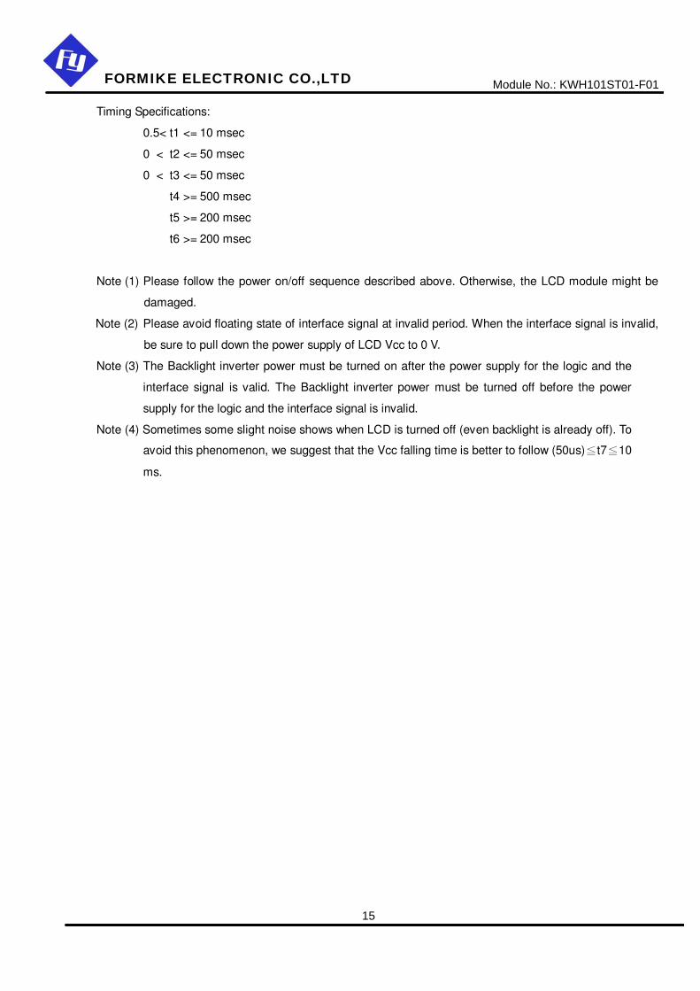
Timing Specifications:
0.5< t1 <= 10 msec
0 < t2 <= 50 msec
0 < t3 <= 50 msec
t4 >= 500 msec
t5 >= 200 msec
t6 >= 200 msec
Note (1) Please follow the power on/off sequence described above. Otherwise, the LCD module might be
damaged.
Note (2) Please avoid floating state of interface signal at invalid period. When the interface signal is invalid,
be sure to pull down the power supply of LCD Vcc to 0 V.
Note (3) The Backlight inverter power must be turned on after the power supply for the logic and the
interface signal is valid. The Backlight inverter power must be turned off before the power
supply for the logic and the interface signal is invalid.
Note (4) Sometimes some slight noise shows when LCD is turned off (even backlight is already off). To
avoid this phenomenon, we suggest that the Vcc falling time is better to follow (50us)�t7�10
ms.
FORMIKE ELECTRONIC CO.,LTD Module No.: KWH101ST01-F01
15
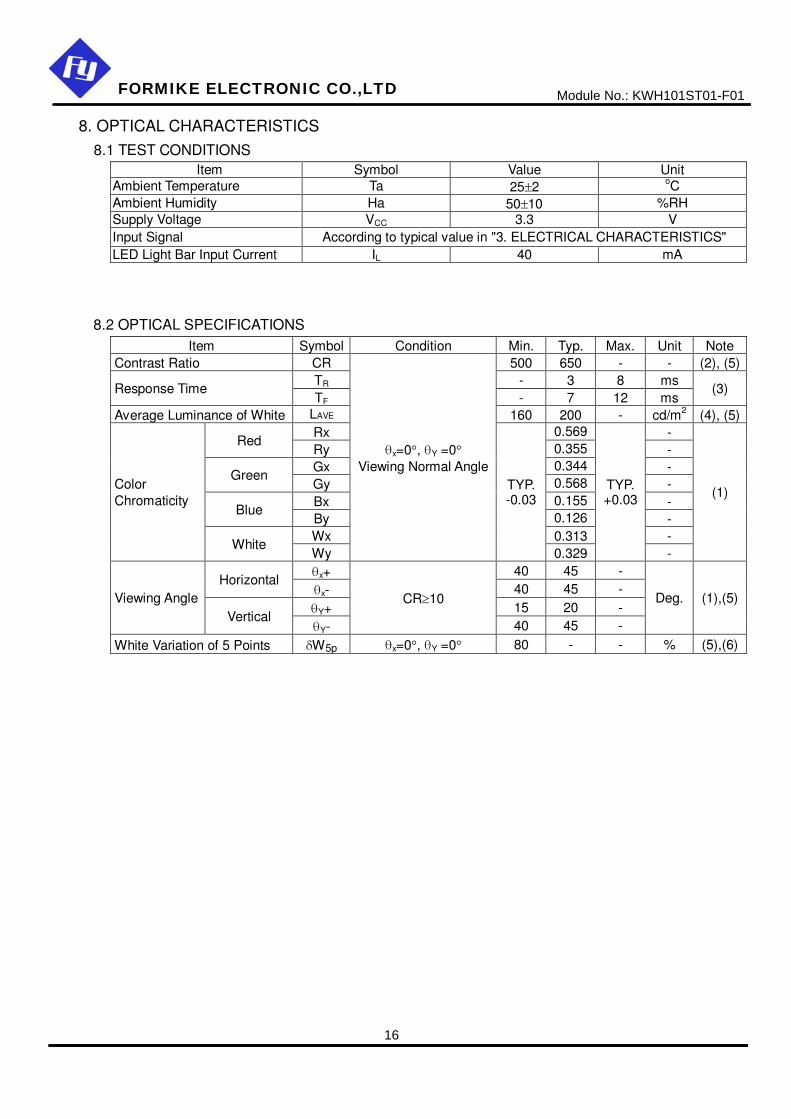
8. OPTICAL CHARACTERISTICS 8.1 TEST CONDITIONS
Item Symbol Value Unit Ambient Temperature Ta 25±2 oC Ambient Humidity Ha 50±10 %RH Supply Voltage VCC 3.3 V Input Signal According to typical value in "3. ELECTRICAL CHARACTERISTICS" LED Light Bar Input Current IL 40 mA
8.2 OPTICAL SPECIFICATIONS Item Symbol Condition Min. Typ. Max. Unit Note
Contrast Ratio CR 500 650 - - (2), (5) TR - 3 8 ms Response Time TF - 7 12 ms
(3)
Average Luminance of White LAVE 160 200 - cd/m2 (4), (5) Rx 0.569 -
Red Ry 0.355 - Gx 0.344 -
Green Gy 0.568 - Bx 0.155 - Blue By 0.126 - Wx 0.313 -
Color Chromaticity
White Wy
θx=0°, θY =0° Viewing Normal Angle
TYP. -0.03
0.329
TYP. +0.03
-
(1)
θx+ 40 45 - Horizontal
θx- 40 45 - θY+ 15 20 -
Viewing Angle Vertical
θY-
CR≥10
40 45 -
Deg. (1),(5)
White Variation of 5 Points δW5p θx=0°, θY =0° 80 - - % (5),(6)
FORMIKE ELECTRONIC CO.,LTD Module No.: KWH101ST01-F01
16
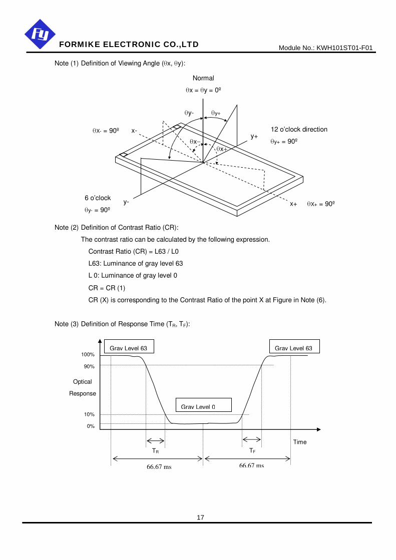
Note (1) Definition of Viewing Angle (θx, θy):
Note (2) Definition of Contrast Ratio (CR):
The contrast ratio can be calculated by the following expression.
Contrast Ratio (CR) = L63 / L0
L63: Luminance of gray level 63
L 0: Luminance of gray level 0
CR = CR (1)
CR (X) is corresponding to the Contrast Ratio of the point X at Figure in Note (6).
Note (3) Definition of Response Time (TR, TF):
12 o’clock direction
θy+ = 90º
6 o’clock
θy- = 90º
θx− θx+
θy- θy+
x- y+
y- x+
Normal
θx = θy = 0º
θX+ = 90º
θX- = 90º
100%
90%
10%
0%
Gray Level 63
Gray Level 0
Gray Level 63
Time TF
Optical
Response
TR
66.67 ms 66.67 ms
FORMIKE ELECTRONIC CO.,LTD Module No.: KWH101ST01-F01
17
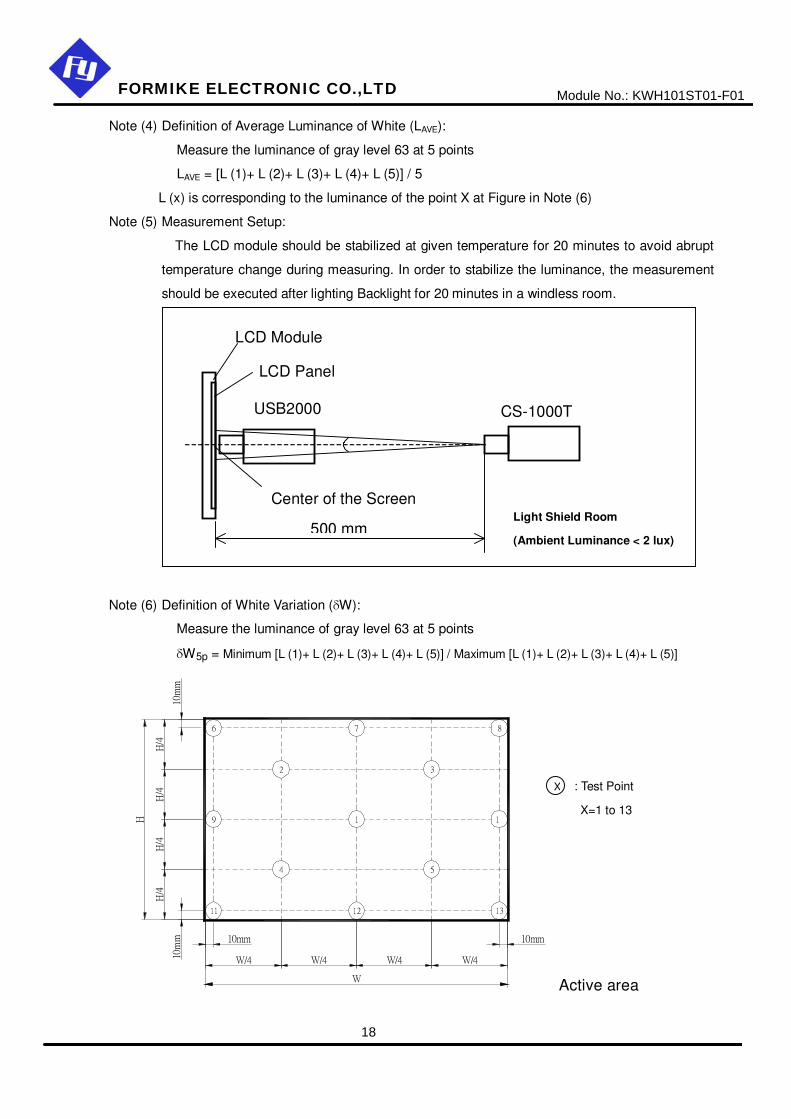
Note (4) Definition of Average Luminance of White (LAVE):
Measure the luminance of gray level 63 at 5 points
LAVE = [L (1)+ L (2)+ L (3)+ L (4)+ L (5)] / 5
L (x) is corresponding to the luminance of the point X at Figure in Note (6)
Note (5) Measurement Setup:
The LCD module should be stabilized at given temperature for 20 minutes to avoid abrupt
temperature change during measuring. In order to stabilize the luminance, the measurement
should be executed after lighting Backlight for 20 minutes in a windless room.
� � � � � � � � � � � �
CS-1000T
500 mm
LCD Module
LCD Panel
Center of the Screen Light Shield Room
(Ambient Luminance < 2 lux)
USB2000
Note (6) Definition of White Variation (δW):
Measure the luminance of gray level 63 at 5 points
δW5p = Minimum [L (1)+ L (2)+ L (3)+ L (4)+ L (5)] / Maximum [L (1)+ L (2)+ L (3)+ L (4)+ L (5)]
� � �
� �
�
� �
�� �� ��
�
�
�
� � � � � � � �
�� � �� � �� � �� �
���
����
���
���
���
����
Active area
: Test Point
X=1 to 13
X
FORMIKE ELECTRONIC CO.,LTD Module No.: KWH101ST01-F01
18
9. PRECAUTIONS
9.1 SYSTEM MATCHING PRECAUTIONS (1) Refer to the drawing.
(2) To avoid wireless noise interference, please keep the antenna away from LCD control board.
9.2 HANDLING PRECAUTIONS (1) The module should be assembled into the system firmly by using every mounting hole. Be careful
not to twist or bend the module.
(2) While assembling or installing modules, it can only be in the clean area. The dust and oil may
cause electrical short or damage the polarizer.
(3) Use fingerstalls or soft gloves in order to keep display clean during the incoming inspection and
assembly process.
(4) Do not press or scratch the surface harder than a HB pencil lead on the panel because the
polarizer is very soft and easily scratched.
(5) If the surface of the polarizer is dirty, please clean it by some absorbent cotton or soft cloth. Do not
use Ketone type materials (ex. Acetone), Ethyl alcohol, Toluene, Ethyl acid or Methyl chloride. It
might permanently damage the polarizer due to chemical reaction.
(6) Wipe off water droplets or oil immediately. Staining and discoloration may occur if they left on
panel for a long time.
(7) If the liquid crystal material leaks from the panel, it should be kept away from the eyes or mouth.
In case of contacting with hands, legs or clothes, it must be washed away thoroughly with soap.
(8) Protect the module from static electricity, it may cause damage to the C-MOS Gate Array IC.
(9) Do not disassemble the module.
(10) Do not pull or fold the lamp wire.
(11) Pins of I/F connector should not be touched directly with bare hands.
9.3 STORAGE PRECAUTIONS
(1) High temperature or humidity may reduce the performance of module. Please store LCD module
within the specified storage conditions.
(2) It is dangerous that moisture come into or contacted the LCD module, because the moisture may
damage LCD module when it is operating.
(3) It may reduce the display quality if the ambient temperature is lower than 10 ºC. For example, the
response time will become slowly, and the starting voltage of lamp will be higher than the room
temperature.
9.4 OPERATION PRECAUTIONS
(1) Do not pull the I/F connector in or out while the module is operating.
(2) Always follow the correct power on/off sequence when LCD module is connecting and operating.
This can prevent the LSI chips from damage during latch-up.
(3) The startup voltage of Backlight is approximately 1000 Volts. It may cause electrical shock while
assembling with inverter. Do not disassemble the module or insert anything into the Backlight unit.
9.5 OTHER PRECAUTIONS (1) When fixed patterns are displayed for a long time, remnant image is likely to occur.
FORMIKE ELECTRONIC CO.,LTD Module No.: KWH101ST01-F01
FORMIKE
19
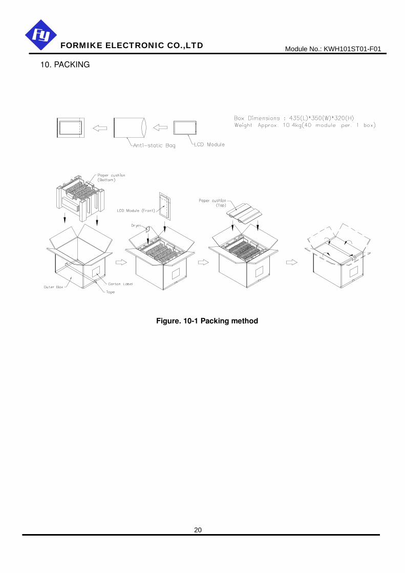
10. PACKING
Figure. 10-1 Packing method
FORMIKE ELECTRONIC CO.,LTD Module No.: KWH101ST01-F01
20