four concepts for synchronous, psn limited, true cds, hdr...
TRANSCRIPT
Four Concepts for Synchronous, PSN limited, true CDS, HDR imaging
A.K.Kalgi, B.Dierickx, B.Dupont, P.Coppejans, P.Gao, B.Spinnewyn, B.Luyssaert, A. Defernez, J. Zhu, J.Basteleus, Q. Yao, W. Verbruggen, D. Uwaerts, B. Uwaerts, G. Ruttens, G. Cai
Caeleste CVBA, Hendrik Consciencestraat 1 b, 2800 Mechelen, Belgium. +32 478 299 757
Introduction In this paper we compare 4 different methods of HDR imaging that have linear response, PSN limited operation at all light levels, true CDS, and are capable of performing synchronous shutter operation. This narrow definition excludes many existing alternative “HDR” methods [1], which fail in one of these specs. Logarithmic response[4], lin-log[5] and multiple slope methods [3] fail because of not being linear or not having a single synchronous integration time. Methods based on varying the integration time or using multiple different size photodiodes fail at having PSN limited operation and methods based on acquiring and combining multiple frames at different gains fail to operate in synchronous shutter mode.
These four methods all have multiple fully linear ranges, where by the higher QFW ranges are reached by means to store excess electrons that do not fit in the PPD or FD. In the “DC overflow” method, such capacitor is connected to the FD via an overflow transistor; in the “push-back” method the additional capacitance is implemented an nMOSFET; in the “3-level TG” method the capacitor is connected via a mere switch; in the “extended FD” method the capacitance of the FD is increased by a MOS capacitor on top of the photodiode.
The DC overflow method
As a reference we start from the method shorthanded here as “DC-overflow” method [2]. After integration, photocharges are transferred to the FD and excess charges can overflow over a DC gate to an additional capacitor. The high gain signal is obtained in the usual way; the low gain signal is obtained by subsequently connecting the large capacitor to the FD.
Figure 2 potential diagram describing the concept of operation of the DC overflow method
CAP
Reset
TG off
CDS
Φ
CAP
CDS
DC
Φ
DCgate
TG Off-On-Off
CAP
Φ TG off
Figure 1 pixel with DC-overflow gate

3 level TG method
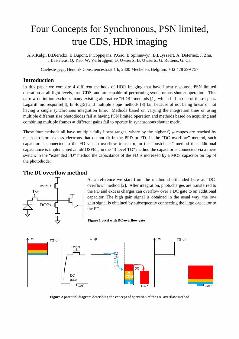
This method starts from an almost identical pixel with the capacitor connected to the FD by a ‘Merge’ switch. The TG, when biased to an intermediate level, performs the function of a DC overflow for the excess electrons generated in the photodiode. The integration moment starts after the pixel is reset. During integration, TG is set to an intermediate voltage so that the excess electrons generated in the photodiode flow through the TG via floating diffusion (FD) into the additional capacitance connected by the Merge transistor. The total charge can thus be much larger than contained in the PPD. After integration, TG and Merge are turned off and the reset level is read out. This reset level “R” may differ from the initial FD reset level; the signal with high gain (small QFW) “S1” is obtained by transfer of charges from photodiode to FD, and this can happen with CDS. Then the low gain signal “S2” is obtained by turning the Merge switch on. Thus 3 FD signal levels are involved obtaining the HDR functionality.
The pixel cross section and 6.5 µm x 6.5 µm pixel layout are shown in Figure 3.
Figure 3. 3-level TG pixel cross section, simplified layout and conceptual mode of operation
Po
ten
tia
l b
arr
ier
φPhoto-charges
FDpinned
diode
TG CAP
ME
RG
E
FDpinned
diode
TG CAP
ME
RG
E
FDpinned
diode
TG CAP
ME
RG
E
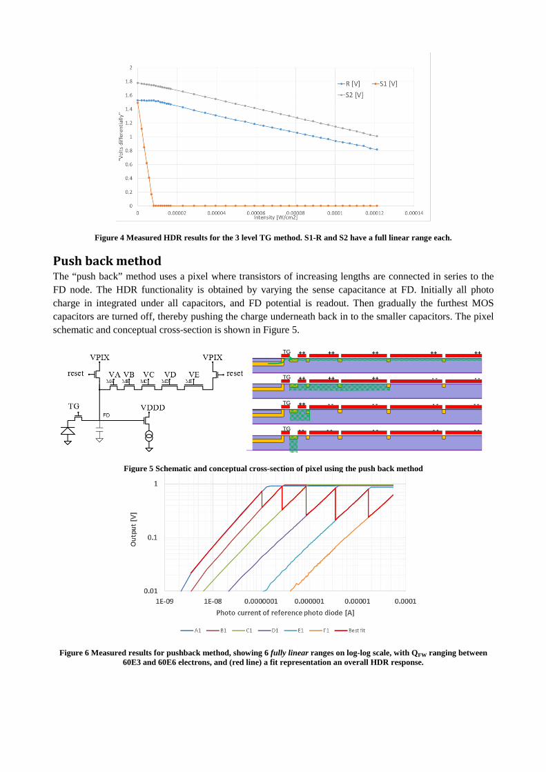
Figure 4 Measured HDR results for the 3 level TG method. S1-R and S2 have a full linear range each.
Push back method
The “push back” method uses a pixel where transistors of increasing lengths are connected in series to the FD node. The HDR functionality is obtained by varying the sense capacitance at FD. Initially all photo charge in integrated under all capacitors, and FD potential is readout. Then gradually the furthest MOS capacitors are turned off, thereby pushing the charge underneath back in to the smaller capacitors. The pixel schematic and conceptual cross-section is shown in Figure 5.
Figure 5 Schematic and conceptual cross-section of pixel using the push back method
Figure 6 Measured results for pushback method, showing 6 fully linear ranges on log-log scale, with QFW ranging between 60E3 and 60E6 electrons, and (red line) a fit representation an overall HDR response.
TG ++ ++ ++ ++ ++
TG ++ ++ ++ - - - -
TG ++ - - - - - - - -
TG - - - - - - - - - -
Extended FD method
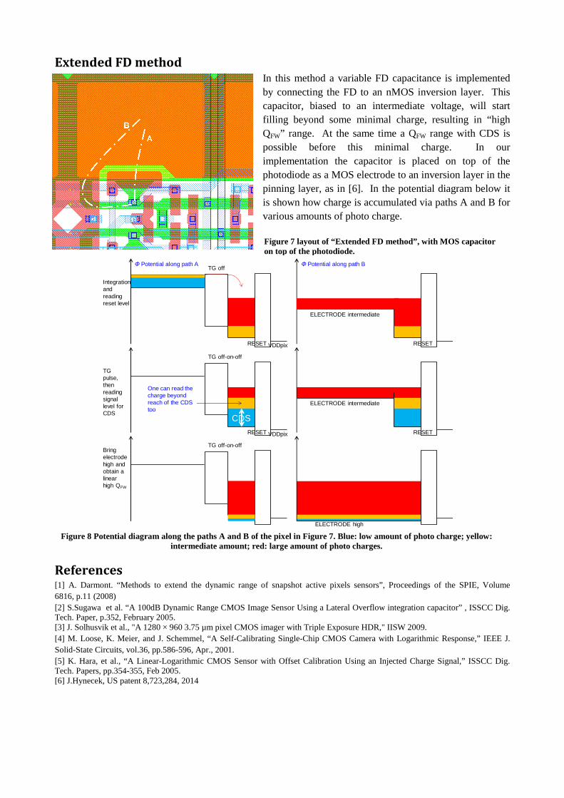
In this method a variable FD capacitance is implemented by connecting the FD to an nMOS inversion layer. This capacitor, biased to an intermediate voltage, will start filling beyond some minimal charge, resulting in “high QFW” range. At the same time a QFW range with CDS is possible before this minimal charge. In our implementation the capacitor is placed on top of the photodiode as a MOS electrode to an inversion layer in the pinning layer, as in [6]. In the potential diagram below it is shown how charge is accumulated via paths A and B for various amounts of photo charge.
Figure 8 Potential diagram along the paths A and B of the pixel in Figure 7. Blue: low amount of photo charge; yellow:
intermediate amount; red: large amount of photo charges.
References
[1] A. Darmont. “Methods to extend the dynamic range of snapshot active pixels sensors”, Proceedings of the SPIE, Volume 6816, p.11 (2008) [2] S.Sugawa et al. “A 100dB Dynamic Range CMOS Image Sensor Using a Lateral Overflow integration capacitor” , ISSCC Dig. Tech. Paper, p.352, February 2005. [3] J. Solhusvik et al., "A 1280 × 960 3.75 µm pixel CMOS imager with Triple Exposure HDR," IISW 2009. [4] M. Loose, K. Meier, and J. Schemmel, “A Self-Calibrating Single-Chip CMOS Camera with Logarithmic Response,” IEEE J. Solid-State Circuits, vol.36, pp.586-596, Apr., 2001. [5] K. Hara, et al., “A Linear-Logarithmic CMOS Sensor with Offset Calibration Using an Injected Charge Signal,” ISSCC Dig. Tech. Papers, pp.354-355, Feb 2005. [6] J.Hynecek, US patent 8,723,284, 2014
TG off
RESET VDDpix RESET
ELECTRODE intermediate
Integration and reading reset level
CDS
TG off-on-off
RESET VDDpix RESET
ELECTRODE intermediate
TG pulse, then reading signal level for CDS
One can read the charge beyond reach of the CDS too
Φ Potential along path A Φ Potential along path B
Bring electrode high and obtain a linear high QFW
TG off-on-off
ELECTRODE high
Figure 7 layout of “Extended FD method”, with MOS capacitor on top of the photodiode.