fpga system bus interface for msc81xx code and discusses user-programmable machine ... dma program...
TRANSCRIPT
Freescale SemiconductorApplication Note
AN2823Rev. 0, 8/2004
CONTENTS
1 Baseband System Example .....................................12 MSC81xx UPM .......................................................42.1 Initializing the UPM ................................................52.2 UPM Read and Write Access Waveforms ..............83 VHDL Code for the FPGA System Bus Interface ..93.1 Top Port Declaration ...............................................93.2 Components (Modules) .........................................103.3 Internal Signals .....................................................113.4 Debug Signals .......................................................113.5 Address Converter .................................................123.6 Bus De-Multiplexer ...............................................123.7 Registering External Signals at the FPGA IOBs
(Optional) ..............................................................123.8 Component Port Mapping .....................................133.9 Digital Clock Management (DCM) ......................133.10 Block DPRAM ......................................................153.11 Xilinx CORE Generator ........................................154 Integrated Software Environment (ISE)
Tool Reports ..........................................................164.1 Synthesis Report ...................................................164.2 Map Report ...........................................................174.3 Place and Route (PAR) Report .............................175 VHDL Code Listing...............................................185.1 top_vhdl.vhd .........................................................185.2 dcm1.vhd ...............................................................21
FPGA System Bus Interface for MSC81xxA VHDL Reference Design
by Dejan Minic
This application note describes how to implement the MSC81xx 60x-compatible system bus interface on the Xilinx® field-programmable gate array (FPGA) using VHDL. VHDL is an acronym that stands for VHSIC hardware description language. VHSIC is yet another acronym that stands for very high speed integrated circuits. This application note introduces the 60x-compatible system bus, referred to simply as the system bus in the remainder of this document, and describes the use of this bus in a generic baseband system. It describes the system bus signals and their connections, as well as the logical architecture of the system bus interface. It closely examines the VHDL code and discusses user-programmable machine (UPM) programming. The document concludes with a listing of the complete VHDL reference code.
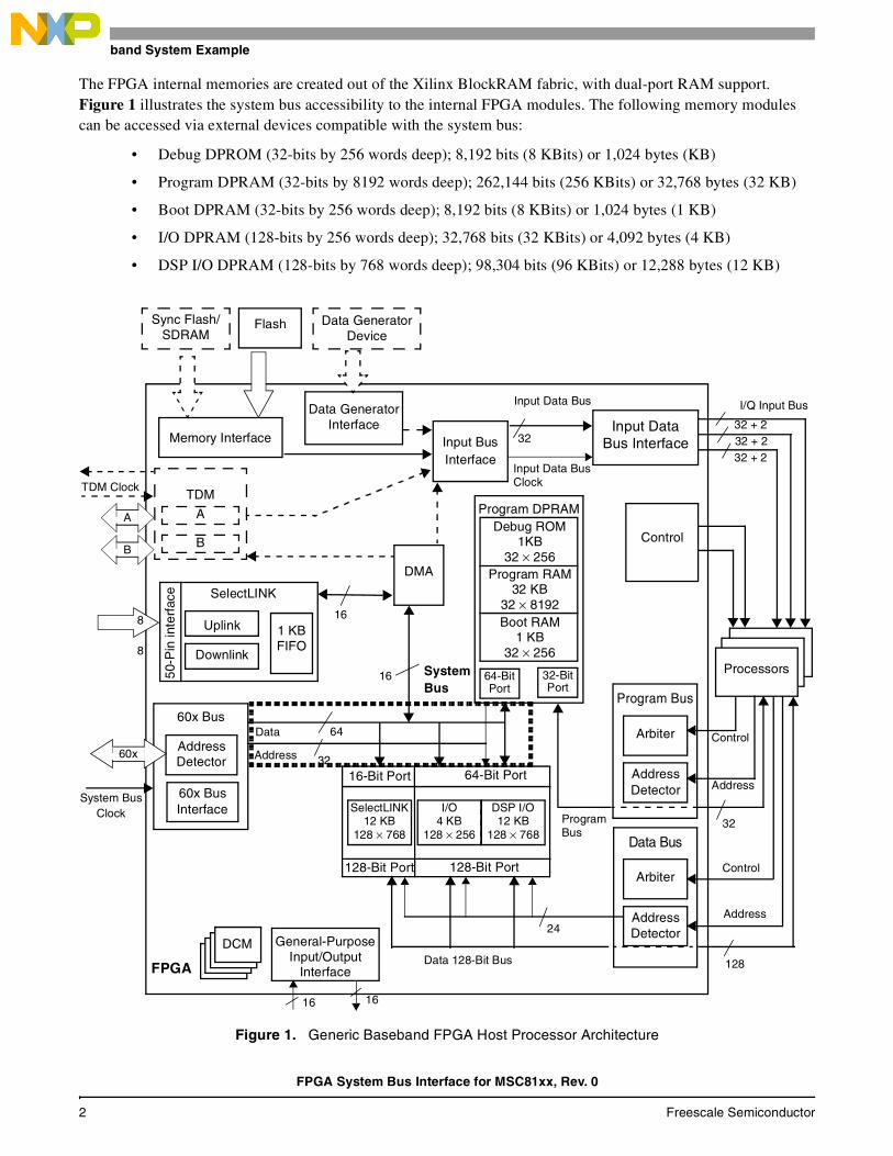
1 Baseband System ExampleFigure 1 illustrates a generic baseband FPGA processor architecture in which the FPGA serves as a host, bus arbiter, and memory to three general-purpose baseband processors. The FPGA is the only interface to the various peripheral devices such as SDRAM, Flash memory, and a data generator (pattern generator). Furthermore, FPGA provides connectivity to the external devices via TDM, SelectLINK™, and the system bus interface. This application note focuses on the system bus interface. In the generic baseband design, the FPGA internal memory gains access to external devices via the system bus interface and is in turn used by the baseband compute processors.
© Freescale Semiconductor, Inc., 2004. All rights reserved.
Baseband System Example
The FPGA internal memories are created out of the Xilinx BlockRAM fabric, with dual-port RAM support. Figure 1 illustrates the system bus accessibility to the internal FPGA modules. The following memory modules can be accessed via external devices compatible with the system bus:
• Debug DPROM (32-bits by 256 words deep); 8,192 bits (8 KBits) or 1,024 bytes (KB)
• Program DPRAM (32-bits by 8192 words deep); 262,144 bits (256 KBits) or 32,768 bytes (32 KB)
• Boot DPRAM (32-bits by 256 words deep); 8,192 bits (8 KBits) or 1,024 bytes (1 KB)
• I/O DPRAM (128-bits by 256 words deep); 32,768 bits (32 KBits) or 4,092 bytes (4 KB)
• DSP I/O DPRAM (128-bits by 768 words deep); 98,304 bits (96 KBits) or 12,288 bytes (12 KB)
Figure 1. Generic Baseband FPGA Host Processor Architecture
Arbiter
AddressDetector
Program Bus
FPGA
ProcessorsProcessors
Processors
Input DataBus Interface
Control
Address
60x BusInterface
60x Bus
Arbiter
AddressDetector
Data Bus
Memory Interface
Sync Flash/SDRAM
Data GeneratorDevice
Flash
Detector
TDM
A
B
Input BusInterface
Data GeneratorInterface
DCMDCMDCMDCM General-PurposeInput/Output
Interface
DMA
Program DPRAM
SelectLINK
1 KBFIFO
Uplink
Downlink
50-P
in in
terf
ace
Debug ROM1KB
32 × 256Program RAM
32 KB32 × 8192Boot RAM
1 KB32 × 256
64-BitPort
32-BitPort
16-Bit Port 64-Bit Port
SelectLINK12 KB
128 × 768
128-Bit Port 128-Bit Port
DSP I/O12 KB
128 × 768
I/O4 KB
128 × 256
Control
Address
Input Data Bus
32
Input Data BusClock
16 16
24
128
32
Data 128-Bit Bus
I/Q Input Bus
32 + 232 + 232 + 2
ProgramBus
Control
Address
Address
Data 64
32
16
16
SystemBus
8
8
System BusClock
TDM Clock
60x
A
B
FPGA System Bus Interface for MSC81xx, Rev. 0
2 Freescale Semiconductor
Baseband System Example
The FPGA internal memory map can be configured as follows:
• Program RAM (32 KB) Start: 0x000000 binary 0000 0000 0000 0000 0000 0000 End: 0x007FFF binary 0000 0000 0111 1111 1111 1111
The FPGA memory/address detector can use the four MSB (0000) to control the memory enable signals. The two LSB can be ignored because the FPGA internal memory is 4-byte addressable.
• I/O RAM (4 KB) Start: 0x300000 binary 0011 0000 0000 0000 0000 0000 End: 0x300FFF binary 0011 0000 0000 1111 1111 1111
The FPGA memory/address detector can use the four MSB (0011) to control the memory enable signals. The two LSB can be ignored because the FPGA internal memory is 4-byte addressable.
• DSP RAM (12 KB) Start: 0x400000 binary 0100 0000 0000 0000 0000 0000 End: 0x402FFF binary 0100 0000 0010 1111 1111 1111
The FPGA memory/address detector can use the four MSB (0100) to control the memory enable signals. The two LSB can be ignored because the FPGA internal memory is 4-byte addressable.
• SelectLINK RAM (12 KB) Start: 0x500000 binary 0101 0000 0000 0000 0000 0000 End: 0x502FFF binary 0101 0000 0010 1111 1111 1111
The FPGA memory/address detector can use the four MSB (0101) to control the memory enable signals. The two LSB can be ignored because the FPGA internal memory is 4-byte addressable.
• CodeWarrior® Debug ROM (1 KB) Start: 0xF00000binary 1111 0000 0000 0000 0000 0000 End: 0xF003FFbinary 1111 0000 0000 0011 1111 1111
The FPGA memory/address detector can use the four MSB (1111) to control the memory enable signals. The two LSB can be ignored because the FPGA internal memory is 4-byte addressable.
In the Freescale MSC81xx DSP devices, the system bus provides flexible communication support between the core and internal/external peripheral devices or other bus masters/slaves. The system bus supports 32-bit addressing for a 32-bit or 64-bit wide data base. The burst mode operation can transfer up to 256 bits of data in a four-beat burst. The system bus also supports 8-bit, 16-bit, and 32-bit data ports. Accesses of 1, 2, 3 and 4 bytes can be aligned or unaligned on 4-byte (word) boundaries. Also, 64-bit, 128-bit, 192-bit, and 256-bit accesses are supported. The address and data buses are set up to handle a one-level pipeline, synchronous transaction. The system bus operates in external and internal master modes. For the reference design discussed in this document, the UPM and system bus are configured as follows:
• 64-bit wide port
• 32-bit addressing
• Synchronous, single access transactions
• Single-Bus mode
In Single-Bus mode the MSC81xx is the only bus master device in the system. The MSC81xx internal memory controller controls all devices on the 60x external pins. In this mode, MSC81xx devices use the address bus as a memory address bus. Slave devices do not have control over the system bus signals.
FPGA System Bus Interface for MSC81xx, Rev. 0
Freescale Semiconductor 3
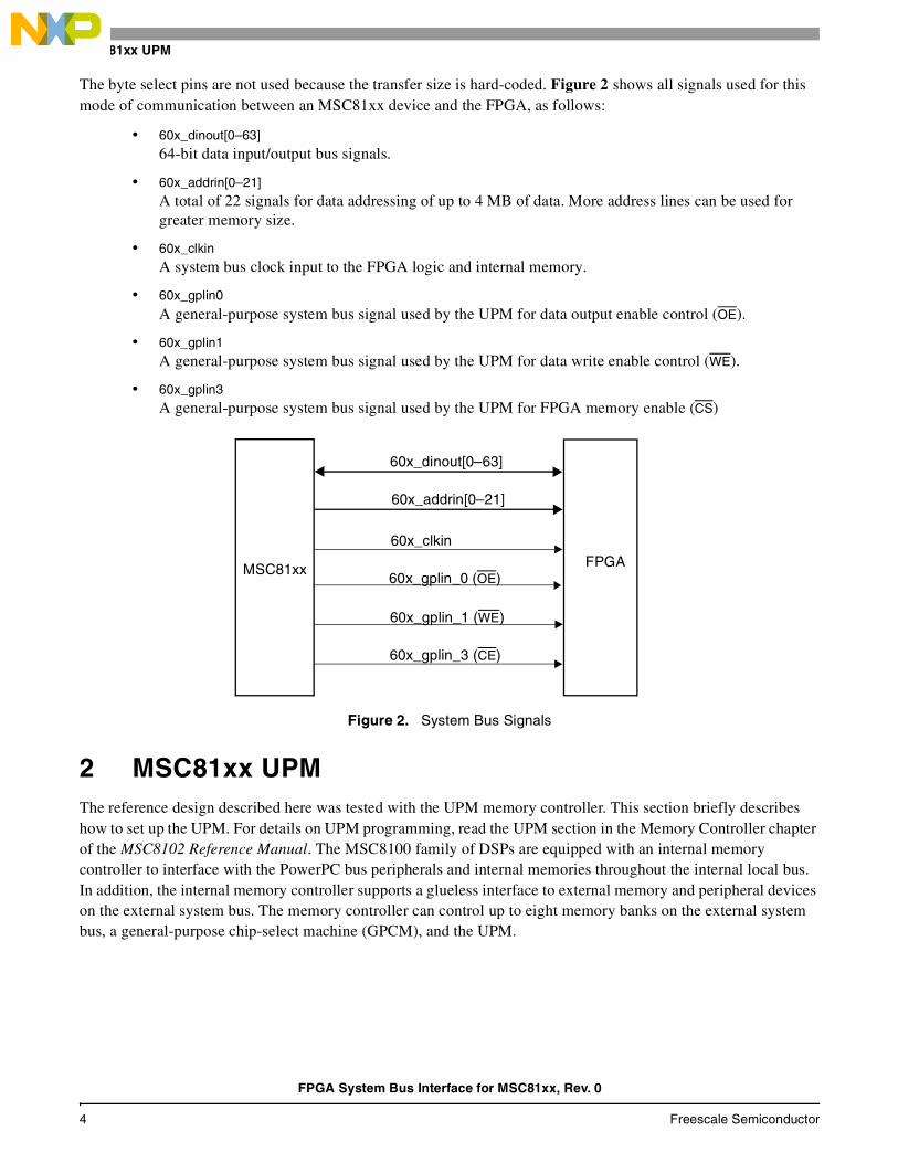
MSC81xx UPM
The byte select pins are not used because the transfer size is hard-coded. Figure 2 shows all signals used for this mode of communication between an MSC81xx device and the FPGA, as follows:
• 60x_dinout[0–63] 64-bit data input/output bus signals.
• 60x_addrin[0–21] A total of 22 signals for data addressing of up to 4 MB of data. More address lines can be used for greater memory size.
• 60x_clkin A system bus clock input to the FPGA logic and internal memory.
• 60x_gplin0 A general-purpose system bus signal used by the UPM for data output enable control (OE).
• 60x_gplin1 A general-purpose system bus signal used by the UPM for data write enable control (WE).
• 60x_gplin3 A general-purpose system bus signal used by the UPM for FPGA memory enable (CS)
Figure 2. System Bus Signals
2 MSC81xx UPMThe reference design described here was tested with the UPM memory controller. This section briefly describes how to set up the UPM. For details on UPM programming, read the UPM section in the Memory Controller chapter of the MSC8102 Reference Manual. The MSC8100 family of DSPs are equipped with an internal memory controller to interface with the PowerPC bus peripherals and internal memories throughout the internal local bus. In addition, the internal memory controller supports a glueless interface to external memory and peripheral devices on the external system bus. The memory controller can control up to eight memory banks on the external system bus, a general-purpose chip-select machine (GPCM), and the UPM.
MSC81xx FPGA
60x_dinout[0–63]
60x_addrin[0–21]
60x_clkin
60x_gplin_0 (OE)
60x_gplin_1 (WE)
60x_gplin_3 (CE)
FPGA System Bus Interface for MSC81xx, Rev. 0
4 Freescale Semiconductor
MSC81xx UPM
2.1 Initializing the UPMTo initialize and program the UPM properly, you must perform the following overall steps:
1. Set up the Base Registers (BRx) and the Option Registers (ORx).
In this example the BR4 and OR4 registers are used. The BR6 and OR6 registers could be used instead. Depending on the system, ten other BR and OR combinations could be used.
2. Write patterns into the RAM array.
3. Program the Memory Refresh Timer Prescaler Register (MPTPR) and the 60x Bus-Assigned UPM Refresh Timer (PURT) register if a refresh is required.
These registers are not programmed in the example discussed here.
4. Program the Machine Mode Register (MxMR).
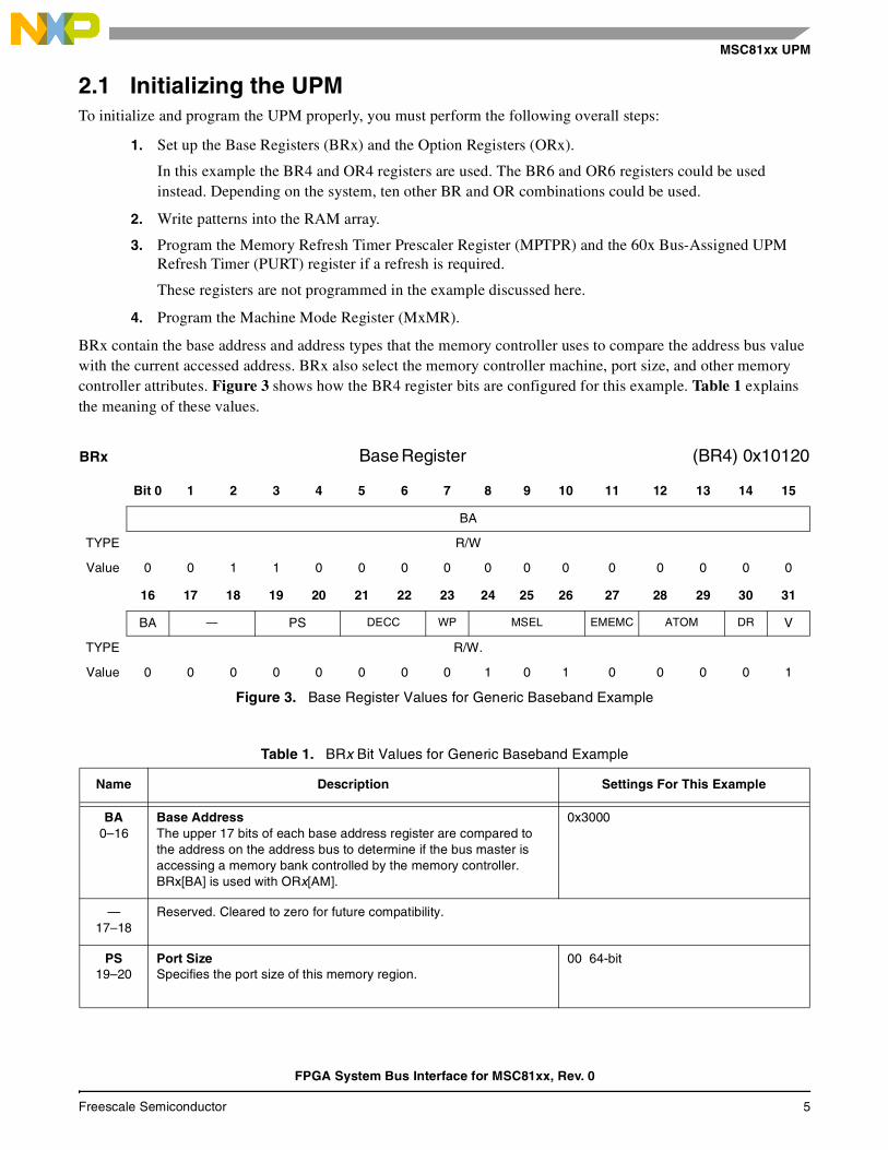
BRx contain the base address and address types that the memory controller uses to compare the address bus value with the current accessed address. BRx also select the memory controller machine, port size, and other memory controller attributes. Figure 3 shows how the BR4 register bits are configured for this example. Table 1 explains the meaning of these values.
BRx Base Register (BR4) 0x10120
Bit 0 1 2 3 4 5 6 7 8 9 10 11 12 13 14 15
BA
TYPE R/W
Value 0 0 1 1 0 0 0 0 0 0 0 0 0 0 0 0
16 17 18 19 20 21 22 23 24 25 26 27 28 29 30 31
BA — PS DECC WP MSEL EMEMC ATOM DR V
TYPE R/W.
Value 0 0 0 0 0 0 0 0 1 0 1 0 0 0 0 1
Figure 3. Base Register Values for Generic Baseband Example
Table 1. BRx Bit Values for Generic Baseband Example
Name Description Settings For This Example
BA0–16
Base AddressThe upper 17 bits of each base address register are compared to the address on the address bus to determine if the bus master is accessing a memory bank controlled by the memory controller. BRx[BA] is used with ORx[AM].
0x3000
—17–18
Reserved. Cleared to zero for future compatibility.
PS19–20
Port SizeSpecifies the port size of this memory region.
00 64-bit
FPGA System Bus Interface for MSC81xx, Rev. 0
Freescale Semiconductor 5
MSC81xx UPM
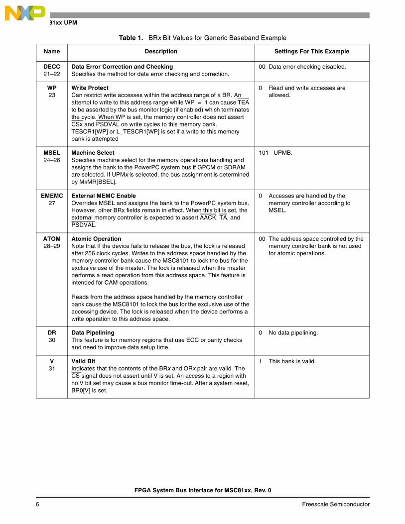
DECC21–22
Data Error Correction and CheckingSpecifies the method for data error checking and correction.
00 Data error checking disabled.
WP23
Write ProtectCan restrict write accesses within the address range of a BR. An attempt to write to this address range while WP = 1 can cause TEA to be asserted by the bus monitor logic (if enabled) which terminates the cycle. When WP is set, the memory controller does not assert CSx and PSDVAL on write cycles to this memory bank. TESCR1[WP] or L_TESCR1[WP] is set if a write to this memory bank is attempted
0 Read and write accesses are allowed.
MSEL24–26
Machine SelectSpecifies machine select for the memory operations handling and assigns the bank to the PowerPC system bus if GPCM or SDRAM are selected. If UPMx is selected, the bus assignment is determined by MxMR[BSEL].
101 UPMB.
EMEMC27
External MEMC EnableOverrides MSEL and assigns the bank to the PowerPC system bus. However, other BRx fields remain in effect. When this bit is set, the external memory controller is expected to assert AACK, TA, and PSDVAL.
0 Accesses are handled by the memory controller according to MSEL.
ATOM28–29
Atomic OperationNote that If the device fails to release the bus, the lock is released after 256 clock cycles. Writes to the address space handled by the memory controller bank cause the MSC8101 to lock the bus for the exclusive use of the master. The lock is released when the master performs a read operation from this address space. This feature is intended for CAM operations.
Reads from the address space handled by the memory controller bank cause the MSC8101 to lock the bus for the exclusive use of the accessing device. The lock is released when the device performs a write operation to this address space.
00 The address space controlled by the memory controller bank is not used for atomic operations.
DR30
Data PipeliningThis feature is for memory regions that use ECC or parity checks and need to improve data setup time.
0 No data pipelining.
V31
Valid BitIndicates that the contents of the BRx and ORx pair are valid. The CS signal does not assert until V is set. An access to a region with no V bit set may cause a bus monitor time-out. After a system reset, BR0[V] is set.
1 This bank is valid.
Table 1. BRx Bit Values for Generic Baseband Example
Name Description Settings For This Example
FPGA System Bus Interface for MSC81xx, Rev. 0
6 Freescale Semiconductor
MSC81xx UPM
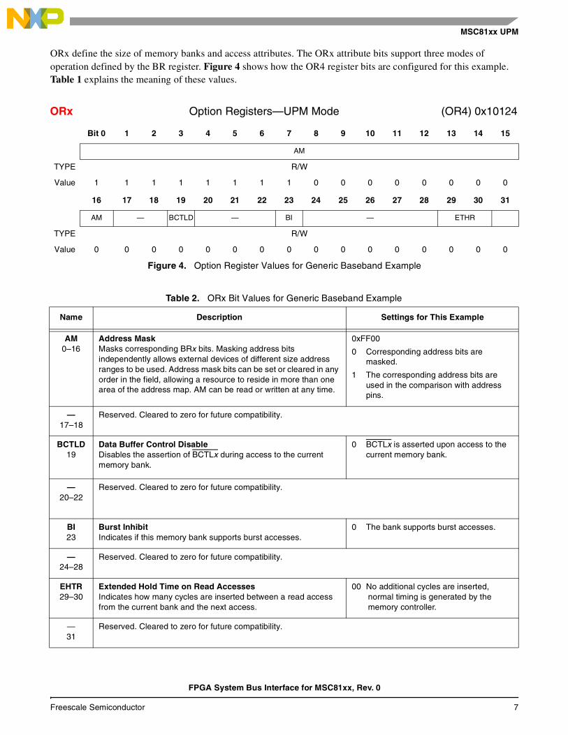
ORx define the size of memory banks and access attributes. The ORx attribute bits support three modes of operation defined by the BR register. Figure 4 shows how the OR4 register bits are configured for this example. Table 1 explains the meaning of these values.
ORx Option Registers—UPM Mode (OR4) 0x10124
Bit 0 1 2 3 4 5 6 7 8 9 10 11 12 13 14 15
AM
TYPE R/W
Value 1 1 1 1 1 1 1 1 0 0 0 0 0 0 0 0
16 17 18 19 20 21 22 23 24 25 26 27 28 29 30 31
AM — BCTLD — BI — ETHR
TYPE R/W
Value 0 0 0 0 0 0 0 0 0 0 0 0 0 0 0 0
Figure 4. Option Register Values for Generic Baseband Example
Table 2. ORx Bit Values for Generic Baseband Example
Name Description Settings for This Example
AM0–16
Address MaskMasks corresponding BRx bits. Masking address bits independently allows external devices of different size address ranges to be used. Address mask bits can be set or cleared in any order in the field, allowing a resource to reside in more than one area of the address map. AM can be read or written at any time.
0xFF00
0 Corresponding address bits are masked.
1 The corresponding address bits are used in the comparison with address pins.
—17–18
Reserved. Cleared to zero for future compatibility.
BCTLD19
Data Buffer Control DisableDisables the assertion of BCTLx during access to the current memory bank.
0 BCTLx is asserted upon access to the current memory bank.
—20–22
Reserved. Cleared to zero for future compatibility.
BI23
Burst InhibitIndicates if this memory bank supports burst accesses.
0 The bank supports burst accesses.
—24–28
Reserved. Cleared to zero for future compatibility.
EHTR29–30
Extended Hold Time on Read AccessesIndicates how many cycles are inserted between a read access from the current bank and the next access.
00 No additional cycles are inserted, normal timing is generated by the memory controller.
—31
Reserved. Cleared to zero for future compatibility.
FPGA System Bus Interface for MSC81xx, Rev. 0
Freescale Semiconductor 7
MSC81xx UPM
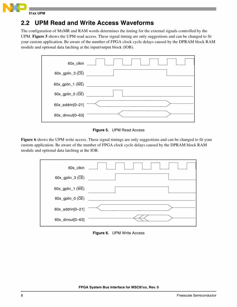
2.2 UPM Read and Write Access WaveformsThe configuration of MxMR and RAM words determines the timing for the external signals controlled by the UPM. Figure 5 shows the UPM read access. These signal timing are only suggestions and can be changed to fit your custom application. Be aware of the number of FPGA clock cycle delays caused by the DPRAM block RAM module and optional data latching at the input/output block (IOB).
Figure 5. UPM Read Access
Figure 6 shows the UPM write access. These signal timings are only suggestions and can be changed to fit your custom application. Be aware of the number of FPGA clock cycle delays caused by the DPRAM block RAM module and optional data latching at the IOB.
Figure 6. UPM Write Access
60x_dinout[0–63]
60x_addrin[0–21]
60x_clkin
60x_gplin_0 (OE)
60x_gplin_1 (WE)
60x_gplin_3 (CE)
60x_dinout[0–63]
60x_addrin[0–21]
60x_clkin
60x_gplin_0 (OE)
60x_gplin_1 (WE)
60x_gplin_3 (CE)
FPGA System Bus Interface for MSC81xx, Rev. 0
8 Freescale Semiconductor
VHDL Code for the FPGA System Bus Interface
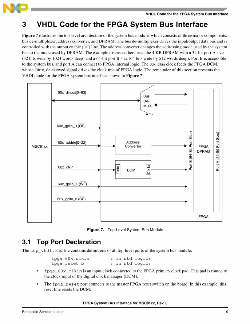
3 VHDL Code for the FPGA System Bus InterfaceFigure 7 illustrates the top-level architecture of the system bus module, which consists of three major components: bus de-multiplexer, address converter, and DPRAM. The bus de-multiplexer drives the input/output data bus and is controlled with the output enable (OE) line. The address converter changes the addressing mode used by the system bus to the mode used by DPRAM. The example discussed here uses the 4 KB DPRAM with a 32-bit port A size (32 bits wide by 1024 words deep) and a 64-bit port B size (64 bits wide by 512 words deep). Port B is accessible to the system bus, and port A can connect to FPGA internal logic. The 60x_clkin clock feeds the FPGA DCM, whose Clk1x, de-skewed signal drives the clock tree of FPGA logic. The remainder of this section presents the VHDL code for the FPGA system bus interface shown in Figure 7.
Figure 7. Top-Level System Bus Module
3.1 Top Port DeclarationThe top_vhdl.vhd file contains definitions of all top-level ports of the system bus module.
fpga_60x_clkin : in std_logic; fpga_reset_b : in std_logic;
• fpga_60x_clkin is an input clock connected to the FPGA primary clock pad. This pad is routed to the clock input of the digital clock manager (DCM).
• The fpga_reset port connects to the master FPGA reset switch on the board. In this example, this reset line resets the DCM.
MSC81xx
FPGA
60x_dinout[0–63]
60x_addrin[0–22]
60x_clkin
60x_gplin_0 (OE)
60x_gplin_1 (WE)
60x_gplin_3 (CE)
Por
t B (
64-B
it P
ort S
ize)
Por
t A (
32-B
it P
ort S
ize)
FPGADPRAM
Bus De-
AddressConverter
DCM
Clk
1x
Clk
In
MUX
FPGA System Bus Interface for MSC81xx, Rev. 0
Freescale Semiconductor 9
VHDL Code for the FPGA System Bus Interface
fpga_60x_dinout : inout std_logic_vector(63 downto 0); fpga_60x_addrin : in std_logic_vector(22 downto 0); fpga_60x_0gplin : in std_logic; fpga_60x_1gplin : in std_logic; fpga_60x_3gplin : in std_logic;
• The fpga_60x_dinout is the 64-bit bidirectional bus that directly connects to the system bus de-multiplexer logic.
• The fpga_60x_addrin is the 23-bit address bus connected to the address converter. Not all address lines are used.
• The fpga_60x_0gplin port is a general-purpose MSC81xx UPM signal for output enable functionality. This signal determines when the FPGA drives the fpga_60x_dinout bus.
• The fpga_60x_1gplin port is a general-purpose MSC81xx UPM signal for write enable functionality. This signal determines whether the bus transaction is read or write.
• The fpga_60x_3gplin port is a general-purpose MSC81xx UPM signal for memory enable or chip select (CS). This signal drives the FPGA DPRAM memory enable/disable (ME) port.
p_addra : IN std_logic_vector(9 downto 0); p_clka : IN std_logic; p_dina : IN std_logic_vector(31 downto 0); p_douta : OUT std_logic_vector(31 downto 0); p_ena : IN std_logic; p_wea : IN std_logic;
The p_addra, p_clk, p_dina, p_douta, p_ena and p_wea signals connect to port A of the FPGA DPRAM and can connect to the rest of the FPGA internal logic or other external or internal bus masters.
test_60x_clkin : out std_logic; test_60x_0gplin : out std_logic; test_60x_1gplin : out std_logic; test_60x_3gplin : out std_logic; test_60x_dinout : out std_logic_vector(63 downto 0); test_60x_addrin : out std_logic_vector(8 downto 0)
The test_60x_clkin, test_60x_0gplin, test_60x_1gplin, test_60x_3gplin, test_60x_dinout, and test_60x_addrin ports are only for debugging, and in this example they are routed to the Mictor connector for viewing on the logic analyzer.
3.2 Components (Modules)To keep the design as simple and straightforward as possible, the number of components is held to minimum. Additional components can be defined for more complex designs. For example, for multiple DPRAM blocks an address detector and address converter require more logic, so an additional module is appropriate. Whatever the level of complexity, the design should be as modular and hierarchical as possible. The first module used in this example is the digital clock manager (DCM) module, which takes an external clock and drives the FPGA BUFGMUX clock distribution tree. This clock tree drives all system bus FPGA logic and FPGA internal memory.
FPGA System Bus Interface for MSC81xx, Rev. 0
10 Freescale Semiconductor
VHDL Code for the FPGA System Bus Interface
component DCM1 is Port (fpga_clock :in std_logic; fpga_reset_b :in std_logic; p_lock out std_logic; p_clk0 out std_logic ); end component;
The second module is dual-port RAM that is fabricated out of the FPGA internal BlockRAM fabric. This is true dual-ported memory, with a different port size.
component dsp_dpram port ( addra : IN std_logic_VECTOR(9 downto 0); addrb : IN std_logic_VECTOR(8 downto 0); clka : IN std_logic; clkb : IN std_logic; dina : IN std_logic_VECTOR(31 downto 0); dinb : IN std_logic_VECTOR(63 downto 0); douta : OUT std_logic_VECTOR(31 downto 0); doutb : OUT std_logic_VECTOR(63 downto 0); ena : IN std_logic; enb : IN std_logic; wea : IN std_logic; web : IN std_logic); end component;
3.3 Internal SignalsAll internal signals (wires) have a prefix of i_ and interconnect the modules and FPGA I/O pins.
signal i_60x_addrb_tmp : std_logic_vector(22 downto 0); signal i_60x_addrb : std_logic_vector(8 downto 0); signal i_60x_din : std_logic_vector(63 downto 0); signal i_60x_dout : std_logic_vector(63 downto 0); signal i_60x_mem_oe : std_logic; signal i_60x_mem_me : std_logic; signal i_60x_mem_we : std_logic; signal nc_p_lock : std_logic; signal i_dcm_60x_clk : std_logic;
3.4 Debug SignalsThe following signals are used only for debugging. In this example these signals are routed to the Mictor connector for logic analyzer viewing.
test_60x_clkin <=i_dcm_60x_clk; test_60x_0gplin <=i_60x_mem_oe; test_60x_1gplin <=i_60x_mem_we; test_60x_3gplin <= i_60x_mem_me; test_60x_addrin <= i_60x_addrb; test_60x_dinout <= i_60x_dout when (i_60x_mem_oe = ’0’) else i_60x_din;
FPGA System Bus Interface for MSC81xx, Rev. 0
Freescale Semiconductor 11
VHDL Code for the FPGA System Bus Interface
3.5 Address ConverterThe address converter converts the address lines to the DPRAM format. In this reference design board, 23 address lines are routed to allow up to 4,194,304 bytes of byte-addressable memory. The DPRAM is 64 bits × 512 words, with 8-byte addressing. Only nine address lines are necessary. Since only one DPRAM is used, the memory detector logic is not necessary in this project, but it can be added by implementing a simple address bit compare/detect logic.
i_60x_addrb(0) <= i_60x_addrb_tmp(21); i_60x_addrb(1) <= i_60x_addrb_tmp(20); i_60x_addrb(2) <= i_60x_addrb_tmp(19); i_60x_addrb(3) <= i_60x_addrb_tmp(18); i_60x_addrb(4) <= i_60x_addrb_tmp(17); i_60x_addrb(5) <= i_60x_addrb_tmp(16); i_60x_addrb(6) <= i_60x_addrb_tmp(15); i_60x_addrb(7) <= i_60x_addrb_tmp(14); i_60x_addrb(8) <= i_60x_addrb_tmp(13);
3.6 Bus De-MultiplexerBecause the external system bus is bidirectional, bus de-multiplexing logic is needed inside the FPGA. The de-multiplexer is controlled by the i_60x_mem_oe signal, which is controlled by the MSC81xx UPM. As long as i_60x_mem_oe is equal to 0, the FPGA drives the system bus. Otherwise, the bus is in a high impedance state.
fpga_60x_dinout <= i_60x_dout when (i_60x_mem_oe = ’0’) else (others => ’Z’); i_60x_din <= fpga_60x_dinout;
3.7 Registering External Signals at the FPGA IOBs (Optional)Logic for the external signals at the input/output blocks (IOBs) is optional, but it can be helpful in certain high-speed designs where the FPGA has difficulty meeting the timing constraints. To achieve higher bus efficiency, this process can be eliminated from the design. In designs that have problems with control and address signal timing, the following process registers the signals at the FPGA IOBs. This process introduces an additional pipeline stage but solves most, if not all, timing problems. Use as necessary, depending on the bus speed, FPGA type, and board design.
REG_60x_PROC : process (i_dcm_60x_clk) begin if i_dcm_60x_clk’event and i_dcm_60x_clk=’0’ then i_60x_mem_oe <= fpga_60x_0gplin; i_60x_mem_we <= fpga_60x_1gplin; i_60x_mem_me <= fpga_60x_3gplin; i_60x_addrb_tmp <= fpga_60x_addrin; end if; end process;
If the additional pipeline stage lowers the bus efficiency below the required level and the design meets timing constraints with this process but fails without it, try changing the synthesis options. Changing the synthesis optimization goal from AREA to SPEED and/or changing the synthesis optimization effort level from NORMAL to HIGH can help meet the timing requirements. In addition, disabling the KEEP HIERARCHY option (flattening the design) can improve overall timing results. The synthesis options REGISTER DUPLICATION, REGISTER BALANCING, and MAX FANOUT can also improve the timing in a design, but they should be tried one at a time because each has the potential to yield even worse timing results.
FPGA System Bus Interface for MSC81xx, Rev. 0
12 Freescale Semiconductor
VHDL Code for the FPGA System Bus Interface
If the timing improves but still does not meet requirements, try changing the map properties. Change the OPTIMIZATION STRATEGY, from AREA to SPEED. The ALLOW LOGIC OPTIMIZATION ACROSS HIERARCHY option also can be beneficial. Changing the place and route EFFORT LEVEL from STANDARD to MEDIUM or HIGH along with increasing the EXTRA EFFORT level usually produces better timing results but increases the place and route build time. At the end of the process, changing the STARTING PLACER COST TABLE and experimenting with MULTI PASS PLACE AND ROUTE
PROPERTIES, specifically: PLACE * ROUTE EFFORT LEVEL (OVERALL), EXTRA EFFORT, NUMBER OF PAR ITERATIONS and NUMBER OF RESULTS TO SAVE significantly increases the compile time but yields better design timing. Depending on the size of your FPGA design and the number of constraints, some synthesis, map, and place and route options consume too much time to be practical, but others do not. Experimenting with a combination of parameters may be necessary to reach the optimal timing for an FPGA design. In some marginal cases, increasing the I/O pin driving strength and/or I/O pin skew rate can be effective.
If the code still does not achieve the timing goal, the problem may lie in the FPGA external pin placement on the board. Incorrect FPGA I/O pin placement can cause long FPGA internal signal delays because of the great distance these signals have to travel within the FPGA.
3.8 Component Port MappingThe two components of our design are digital clock management (DCM) and DPRAM. The DCM component is highly simplified due to the simplicity of the design. For the DPRAM component, the system bus uses port B, and port A is available for another bus master or internal FPGA logic.
DCM1_PMAP : DCM1 Port map ( fpga_clock => fpga_60x_clkin, fpga_reset_b => fpga_reset_b, p_lock => nc_p_lock, p_clk0 => i_dcm_60x_clk );
DSP_DPRAM_PMAP : dsp_dpram port map ( addra => p_addra, addrb => i_60x_addrb, clka => p_clka, clkb => i_dcm_60x_clk, dina => p_dina, dinb => i_60x_din, douta => p_douta, doutb => i_60x_dout, ena => p_ena, enb => i_60x_mem_me, wea => p_wea, web => i_60x_mem_we ); end Behavioral;
3.9 Digital Clock Management (DCM)DCM is a standard feature in the Xilinx Virtex-II™, Virtex-II Pro™, and Spartan III® devices. Different models of these devices have different numbers of clock managers. The main features are clock de-skewing, frequency synthesis, phase shifting, and duty cycle correction. Our design uses only clock de-skewing and duty cycle
FPGA System Bus Interface for MSC81xx, Rev. 0
Freescale Semiconductor 13
VHDL Code for the FPGA System Bus Interface
correction. To keep the reference design simple, only clock input, clock output, and clock reset signals are used. Other signals such as lock, status, and other clock outputs should be used in a larger design. The lock signal is the most important and should be routed to the master FPGA control/boot block. This block should keep all FPGA logic in the reset state until the lock signal goes high to indicate that the DCM DLL is locked and the clock output signal is stable. Until the lock signal activates, the DCM output clocks are not valid and can exhibit glitches, spikes, or other unwanted spurious signals.
DLL_FREQUENCY_MODE : string := "LOW"; DUTY_CYCLE_CORRECTION : boolean := TRUE; STARTUP_WAIT : boolean := TRUE
attribute DLL_FREQUENCY_MODE : string; attribute DUTY_CYCLE_CORRECTION : string; attribute STARTUP_WAIT : string; attribute DLL_FREQUENCY_MODE of U_DCM: label is "LOW"; attribute DUTY_CYCLE_CORRECTION of U_DCM: label is "TRUE"; attribute STARTUP_WAIT of U_DCM: label is "TRUE";
These parameters set up the DCM for low frequency operation with the duty cycle correction enabled (50/50) and start-up sequence wait enabled.
p_lock <= i_lock; p_clk0 <= i_clk0; reset <= not (fpga_reset_b);
The i_lock and i_clk0 signals are routed to the DCM output ports for use in the top-level design. The reset signal is inverted because DCM is active high and the master FPGA switch on the board in this reference design is active low.
-- DCM Instantiation U_DCM: DCM port map ( CLKIN => fpga_clock, CLKFB => i_clk0, DSSEN => gnd, PSINCDEC => gnd, PSEN => gnd, PSCLK => gnd, RST => reset, CLK0 => i_clk0_tmp, LOCKED => i_lock );
Notice that the i_clk0 signal is routed to both CLKFB and rest of the FPGA system bus logic. This signal is an output of the global clock buffer, BUFG, and must be routed to the CLKFB port on the DCM component for proper operation of the feedback circuit. In the following BUFG instantiation, notice that i_clk0_tmp is a de-skewed output DCM signal serving as an input to the BUFG. The output of the BUFG is the clock signal to drive the rest of the FPGA logic.
FPGA System Bus Interface for MSC81xx, Rev. 0
14 Freescale Semiconductor
VHDL Code for the FPGA System Bus Interface
-- BUFG Instantiation U1_BUFG: BUFG port map (
I => i_clk0_tmp, O => i_clk0 );
3.10 Block DPRAMThe Xilinx CORE Generator™ created the dual-ported random access memory (DPRAM) module used in the reference design. Each memory port has an address bus, a data input bus, a data output bus, an individual clock signal, an individual memory enable signal, and an individual write enable signal. The difference between port A and B is in the port size. Port A is 32 bits wide and port B is 64 bits wide. The port size influences memory depth, so port A has 10 address lines and port B has 9 address lines.
Check: Port A -> (2^10) address lines * 32 bits port size = 32,768 bits = 4,096 bytesPort B -> (2^9) address lines * 64 bits port size = 32,768 bits = 4,096 bytes
component dsp_dpram port ( addra : IN std_logic_VECTOR(9 downto 0); addrb : IN std_logic_VECTOR(8 downto 0); clka : IN std_logic; clkb : IN std_logic; dina : IN std_logic_VECTOR(31 downto 0); dinb : IN std_logic_VECTOR(63 downto 0); douta : OUT std_logic_VECTOR(31 downto 0); doutb : OUT std_logic_VECTOR(63 downto 0); ena : IN std_logic; enb : IN std_logic; wea : IN std_logic; web : IN std_logic); end component;
The addra, clka, dina, douta, ena, wea signals are port A signals and are routed to the system bus module top ports for usage within the FPGA. The addrb is a port B address bus and is driven by the MSC81xx, along with enb (memory enable) and web (write enable) signals. The clkb is a input clock signal and is the de-skewed version of the system bus input clock signal. The dinb and doutb signals are data input and output bus signals that are routed to the de-multiplexer module.
3.11 Xilinx CORE GeneratorTo create or modify the DPRAM core using the Xilinx CORE Generator, select the core in the source window within the Xilinx Project Navigator. Next, in the Process window run MANAGE CORES within the Coregen process. The Xilinx CORE Generator application launches, and you can chose either to edit or create a new core. The design core window for the dual-port block memory is straightforward. On the first page, set the width of port A to 32 bits and the depth to 1024. Set the width of port B to 64 bits and the depth to 512. Port A and port B options for configuration should be set to READ AND WRITE and for write mode should be set to READ AND WRITE.
FPGA System Bus Interface for MSC81xx, Rev. 0
Freescale Semiconductor 15
Integrated Software Environment (ISE) Tool Reports
On the second core design page for port A, select ENABLE PIN. The HANDSHAKING PIN and REGISTER INPUT features are not used. In the output register options, set the ADDITIONAL OUTPUT PIPE STAGES to 0. The SINIT PIN functionality is not used, so the initialization value (hexadecimal) can be left blank. The pin polarity options are RISING EDGE TRIGGERED for an active clock edge, ACTIVE HIGH for the enable pin, and ACTIVE HIGH for the write enable pin.
On the third core design page for port B, select the optional ENABLE PIN. The HANDSHAKING PIN and REGISTER INPUT features are not used. In the output register options, set the ADDITIONAL OUTPUT PIPE STAGES to 0. The SINIT PIN functionality is not used, so the initialization value (hexadecimal) can be left blank. The pin polarity options are RISING EDGE TRIGGERED for active clock edge, ACTIVE HIGH for the enable pin, and ACTIVE HIGH for the write enable pin.
On the final, fourth core design page within the Initial Contents, the global initialization value is set to 0, but it can be set to any value desired. You can preload the memory with the initialization hexadecimal file (.coe), which can be useful in debugging. If desired, check the LOAD INIT FILE check box and load the initialization hexadecimal file. The bottom of this page presents the summary of the designed DPRAM core. For our example, the information panel should display as follows:
Address Width A10Address Width B9Blocks Used 2Port A Read Pipeline Latency 1 Port B Read Pipeline Latency 2If correct click Generate and the new core will be generated.
4 Integrated Software Environment (ISE) Tool ReportsThis section briefly discusses the tool reports for physical synthesis, mapping the logical design to the FPGA, and assessing the performance of various components to prevent/correct timing problems.
4.1 Synthesis ReportThe beginning of the synthesis report displays the options summary so that you can review the options for synthesis. The HDL compilation, HDL analysis, and HDL synthesis sections contain the warnings and error messages. The last section reports on macro usage, which, in our case, should display: 4 total registers (3 1-bit registers and 1 23-bit register), 1 multiplexer (1 2-to-1 multiplexer) and 1 64-bit tri-state buffer. The final report for this design should display as follows:
246 total IOs, 4 registers, 1 multiplexer, 1 tristate buffer, 67 BELs, 88 FlipFlops/Latches, RAMS, 2 clock buffers, 1 DCM and 231 IO buffers.
The device use summary for the 2v3000b957-4 FPGA model used in this design should read as follows:
Number of Slices: 51 out of 14336 0% Number of Slice Flip Flops: 88 out of 28672 0% Number of 4 input LUTs: 65 out of 28672 0% Number of bonded IOBs: 231 out of 684 33% Number of BRAMs: 2 out of 96 2% Number of GCLKs: 2 out of 16 12% Number of DCMs: 1 out of 12 8%
Next, the timing summary is displayed. This is only a synthesis estimate, but it can prove very useful in predicting the performance of the map and place and route, without the need to run them.
FPGA System Bus Interface for MSC81xx, Rev. 0
16 Freescale Semiconductor
Integrated Software Environment (ISE) Tool Reports
4.2 Map ReportThe map process maps the logical design to a Xilinx FPGA. The input to this process is an NGD file, which contains a logical description of the design in terms of its logical components and lower-level Xilinx primitives. The map process begins with a logical design rule check (DRC) on the design in the NGD file. If the design does not contain any rule violations, the design logic is mapped to the FPGA components of the target FPGA. The output map process is the NCD file, which is used for the place and route process.
The first two sections of the map report are reserved for errors and warnings. The rest of the report is not visible if there are any design rule check errors. Section 3 and 4 of the map report provide information on any removed (optimized) logic. In some cases, the map tool can eliminate the unused logic or FPGA resource, which can produce unwanted effects. Section 6 displays the IOB properties of external FPGA pin declarations. Notice that the fpga_60x_dinout[0–63] pins are declared as bidirectional.
4.3 Place and Route (PAR) ReportIf there are timing problems, the PAR report is the most frequently visited report. As long as the design is successfully mapped to the FPGA and the NCD file is successfully generated, the place and route process is performed. The beginning of the report yields a very helpful device usage summary report. Our design uses a total of 232 out of 684 external IOBs. After the UCF file is created, the number of LOCed external IOBs should read as 232 out of 232. Our design uses two out of 96 RAMB16s and 32 out of 14336 slices. It uses two out of 16 BUFGMUXs and 1 DCM. The next section of the PAR report indicates the phases and how many iterations the PAR performed, which depends on the PAR parameter settings.
The last section of the PAR report is the generating clock report, which contains a very useful clock summary. The fanout for each clock tree used in the design and the associated net skew and maximum delay are some of the most important parameters. This section summarizes any timing violations and timing constraints. If your design does not meet your timing requirements, this section displays the tree in which the violations occurred and provides measurements of the violations.
FPGA System Bus Interface for MSC81xx, Rev. 0
Freescale Semiconductor 17
VHDL Code Listing
5 VHDL Code ListingThis section lists the code in the top_vhdl.vhd and dcm1.vhd files.
5.1 top_vhdl.vhd--*****************************************************************************
--* Property of Freescale, RF and DSP Infrastructure Division --***************************************************************************** --* VHDL source code --* Project Name: Aquarius FPGA --***************************************************************************** --***************************************************************************** --* FILE NAME: top_vhdl.vhd --***************************************************************************** --* DESCRIPTION :Top vhdl module for system bus interface --* AUTHOR : DGM --* VERSION : ISE 6.0.03 --* SYNTHESIZER : XST --* TARGET : XC2V3000-4C-BF957 --***************************************************************************** --* REVISION HISTORY: --***************************************************************************** library IEEE; use IEEE.STD_LOGIC_1164.ALL; use IEEE.STD_LOGIC_ARITH.ALL; use IEEE.STD_LOGIC_UNSIGNED.ALL; -- Uncomment the following lines to use the declarations that are -- provided for instantiating Xilinx primitive components. --library UNISIM; --use UNISIM.VComponents.all;
entity top_vhdl is Port ( fpga_60x_clkin : in std_logic; fpga_reset_b : in std_logic;
-- system bus Interface ********************************************************** fpga_60x_dinout : inout std_logic_vector(63 downto 0); fpga_60x_addrin : in std_logic_vector(22 downto 0);
fpga_60x_0gplin : in std_logic;-- OE fpga_60x_1gplin : in std_logic;-- WE fpga_60x_3gplin : in std_logic;-- CS
--* Internal DPRAM port A signals ********************************************* p_addra : IN std_logic_vector(9 downto 0); p_clka : IN std_logic; p_dina : IN std_logic_vector(31 downto 0); p_douta : OUT std_logic_vector(31 downto 0); p_ena : IN std_logic; p_wea : IN std_logic;
FPGA System Bus Interface for MSC81xx, Rev. 0
18 Freescale Semiconductor
VHDL Code Listing
test_60x_clkin : out std_logic; test_60x_0gplin : out std_logic; test_60x_1gplin : out std_logic; test_60x_3gplin : out std_logic; test_60x_dinout : out std_logic_vector(63 downto 0); test_60x_addrin : out std_logic_vector(8 downto 0) );
end top_vhdl;
architecture Behavioral of top_vhdl is
component DCM1 is Port (
fpga_clock : in std_logic; fpga_reset_b : in std_logic; p_lock : out std_logic; p_clk0 : out std_logic
); end component;
component dsp_dpram port ( addra : IN std_logic_VECTOR(9 downto 0); addrb : IN std_logic_VECTOR(8 downto 0); clka : IN std_logic; clkb : IN std_logic; dina : IN std_logic_VECTOR(31 downto 0); dinb : IN std_logic_VECTOR(63 downto 0); douta : OUT std_logic_VECTOR(31 downto 0); doutb : OUT std_logic_VECTOR(63 downto 0); ena : IN std_logic; enb : IN std_logic; wea : IN std_logic; web : IN std_logic);
end component; -- XST black box declaration --attribute box_type : string; --attribute box_type of dsp_dpram: component is "black_box"; signal i_60x_addrb_tmp : std_logic_vector(22 downto 0); signal i_60x_addrb : std_logic_vector(8 downto 0); signal i_60x_din : std_logic_vector(63 downto 0); signal i_60x_dout : std_logic_vector(63 downto 0); signal i_60x_mem_oe : std_logic; signal i_60x_mem_me : std_logic; signal i_60x_mem_we : std_logic; signal nc_p_lock : std_logic; signal i_dcm_60x_clk : std_logic;
begin --* DEBUG ONLY **************************************************************** test_60x_clkin <= i_dcm_60x_clk; test_60x_0gplin <= i_60x_mem_oe; test_60x_1gplin <= i_60x_mem_we; test_60x_3gplin <= i_60x_mem_me; test_60x_addrin <= i_60x_addrb;
FPGA System Bus Interface for MSC81xx, Rev. 0
Freescale Semiconductor 19
VHDL Code Listing
test_60x_dinout <= i_60x_dout when (i_60x_mem_oe = ’0’) else i_60x_din;
--* ADDRESS CONVERTER ********************************************************* i_60x_addrb(0) <= i_60x_addrb_tmp(21); -- was (22) i_60x_addrb(1) <= i_60x_addrb_tmp(20); i_60x_addrb(2) <= i_60x_addrb_tmp(19); i_60x_addrb(3) <= i_60x_addrb_tmp(18); i_60x_addrb(4) <= i_60x_addrb_tmp(17); i_60x_addrb(5) <= i_60x_addrb_tmp(16); i_60x_addrb(6) <= i_60x_addrb_tmp(15); i_60x_addrb(7) <= i_60x_addrb_tmp(14); i_60x_addrb(8) <= i_60x_addrb_tmp(13); --* BUS DE-MUX ***************************************************************** fpga_60x_dinout <= i_60x_dout when (i_60x_mem_oe = ’0’) else (others => ’Z’); i_60x_din <= fpga_60x_dinout;
REG_60x_PROC : process (i_dcm_60x_clk) begin
if i_dcm_60x_clk’event and i_dcm_60x_clk=’0’ then i_60x_mem_oe <= fpga_60x_0gplin; i_60x_mem_we <= fpga_60x_1gplin; i_60x_mem_me <= fpga_60x_3gplin; i_60x_addrb_tmp <= fpga_60x_addrin;
end if; end process;
DCM1_PMAP : DCM1 Port map (
fpga_clock => fpga_60x_clkin, fpga_reset_b => fpga_reset_b, p_lock => nc_p_lock, p_clk0 => i_dcm_60x_clk
);
DSP_DPRAM_PMAP : dsp_dpram port map ( addra => p_addra, addrb => i_60x_addrb, clka => p_clka, clkb => i_dcm_60x_clk, dina => p_dina, dinb => i_60x_din, douta => p_douta, doutb => i_60x_dout, ena => p_ena, enb => i_60x_mem_me, wea => p_wea, web => i_60x_mem_we );
end Behavioral;
FPGA System Bus Interface for MSC81xx, Rev. 0
20 Freescale Semiconductor
VHDL Code Listing
5.2 dcm1.vhd--*****************************************************************************
--* Property of Freescale, RF and DSP Infrastructure Division --***************************************************************************** --* VHDL source code --* Project Name: Aquarius FPGA --***************************************************************************** --***************************************************************************** --* FILE NAME: dcm_60x.vhd --***************************************************************************** --* DESCRIPTION :DCM module for system bus interface --* AUTHOR : DGM --* VERSION : ISE 6.0.03 --* SYNTHESIZER : XST --* TARGET : XC2V3000-4C-BF957 --***************************************************************************** --* REVISION HISTORY: --***************************************************************************** library IEEE; use IEEE.STD_LOGIC_1164.ALL; use IEEE.STD_LOGIC_ARITH.ALL; use IEEE.STD_LOGIC_UNSIGNED.ALL; -- Uncomment the following lines to use the declarations that are -- provided for instantiating Xilinx primitive components. library UNISIM; use UNISIM.VComponents.all;
entity DCM1 is Port (
fpga_clock : in std_logic; fpga_reset_b : in std_logic; p_lock : out std_logic; p_clk0 : out std_logic
);end DCM1; architecture Behavioral of DCM1 is --***************************************************************************** -- Components Declarations --***************************************************************************** component BUFG
port ( I : in std_logic;
O : out std_logic );
end component;
component DCM -- synopsys translate_off generic ( DLL_FREQUENCY_MODE : string := "LOW"; DUTY_CYCLE_CORRECTION : boolean := TRUE; STARTUP_WAIT : boolean := TRUE ); -- synopsys translate_on port ( CLKIN : in std_logic;
FPGA System Bus Interface for MSC81xx, Rev. 0
Freescale Semiconductor 21
VHDL Code Listing
CLKFB : in std_logic; DSSEN : in std_logic; PSINCDEC : in std_logic; PSEN : in std_logic; PSCLK : in std_logic; RST : in std_logic; CLK0 : out std_logic; CLK90 : out std_logic; CLK180 : out std_logic; CLK270 : out std_logic; CLK2X : out std_logic; CLK2X180 : out std_logic; CLKDV : out std_logic; CLKFX : out std_logic; CLKFX180 : out std_logic; LOCKED : out std_logic; PSDONE : out std_logic; STATUS : out std_logic_vector(7 downto 0) ); end component; -- Attributes attribute DLL_FREQUENCY_MODE : string; attribute DUTY_CYCLE_CORRECTION : string; attribute CLKFX_MULTIPLY : integer; attribute CLKFX_DIVIDE : integer; attribute STARTUP_WAIT : string; attribute DLL_FREQUENCY_MODE of U_DCM: label is "LOW"; attribute DUTY_CYCLE_CORRECTION of U_DCM: label is "TRUE"; attribute STARTUP_WAIT of U_DCM : label is "TRUE"; --***************************************************************************** -- Signal Declarations --***************************************************************************** signal gnd : std_logic; signal i_clk0 : std_logic; signal i_clk0_tmp : std_logic; signal i_lock : std_logic; signal reset : std_logic;
begin
gnd <= ’0’; p_lock <= i_lock; p_clk0 <= i_clk0; reset <= not (fpga_reset_b); -- DCM Instantiation U_DCM: DCM port map ( CLKIN => fpga_clock, CLKFB => i_clk0, DSSEN => gnd, PSINCDEC => gnd, PSEN => gnd, PSCLK => gnd,
FPGA System Bus Interface for MSC81xx, Rev. 0
22 Freescale Semiconductor
VHDL Code Listing
RST => reset, CLK0 => i_clk0_tmp, LOCKED => i_lock ); -- BUFG Instantiation U1_BUFG: BUFG port map (
I => i_clk0_tmp, O => i_clk0 ); end Behavioral
FPGA System Bus Interface for MSC81xx, Rev. 0
Freescale Semiconductor 23
How to Reach Us:
Home Page:www.freescale.com
E-mail:[email protected]
USA/Europe or Locations Not Listed:Freescale SemiconductorTechnical Information Center, CH3701300 N. Alma School Road Chandler, Arizona 85224 +1-800-521-6274 or [email protected]
Europe, Middle East, and Africa:Freescale Halbleiter Deutschland GmbHTechnical Information CenterSchatzbogen 781829 Muenchen, Germany+44 1296 380 456 (English)+46 8 52200080 (English)+49 89 92103 559 (German)+33 1 69 35 48 48 (French)[email protected]
Japan:Freescale Semiconductor Japan Ltd. Technical Information Center 3-20-1, Minami-Azabu, Minato-ku Tokyo 106-0047, Japan 0120 191014 or +81 3 3440 [email protected]
Asia/Pacific:Freescale Semiconductor Hong Kong Ltd.Technical Information Center 2 Dai King Street Tai Po Industrial Estate Tai Po, N.T., Hong Kong +800 2666 [email protected]
For Literature Requests Only:Freescale Semiconductor Literature Distribution CenterP.O. Box 5405Denver, Colorado 802171-800-441-2447 or 303-675-2140Fax: [email protected]
Freescale™ and the Freescale logo are trademarks of Freescale Semiconductor, Inc. All other product or service names are the property of their respective owners.
© Freescale Semiconductor, Inc. 2004. All rights reserved.
AN2823Rev. 08/2004
Information in this document is provided solely to enable system and software implementers to use Freescale Semiconductor products. There are no express or implied copyright licenses granted hereunder to design or fabricate any integrated circuits or integrated circuits based on the information in this document.
Freescale Semiconductor reserves the right to make changes without further notice to any products herein. Freescale Semiconductor makes no warranty, representation or guarantee regarding the suitability of its products for any particular purpose, nor does Freescale Semiconductor assume any liability arising out of the application or use of any product or circuit, and specifically disclaims any and all liability, including without limitation consequential or incidental damages. “Typical” parameters that may be provided in Freescale Semiconductor data sheets and/or specifications can and do vary in different applications and actual performance may vary over time. All operating parameters, including “Typicals”, must be validated for each customer application by customer’s technical experts. Freescale Semiconductor does not convey any license under its patent rights nor the rights of others. Freescale Semiconductor products are not designed, intended, or authorized for use as components in systems intended for surgical implant into the body, or other applications intended to support or sustain life, or for any other application in which the failure of the Freescale Semiconductor product could create a situation where personal injury or death may occur. Should Buyer purchase or use Freescale Semiconductor products for any such unintended or unauthorized application, Buyer shall indemnify and hold Freescale Semiconductor and its officers, employees, subsidiaries, affiliates, and distributors harmless against all claims, costs, damages, and expenses, and reasonable attorney fees arising out of, directly or indirectly, any claim of personal injury or death associated with such unintended or unauthorized use, even if such claim alleges that Freescale Semiconductor was negligent regarding the design or manufacture of the part.