fpga two day beginners workshop instructors · fpga two day beginners workshop instructors 1 craig...
TRANSCRIPT

FPGA Two Day Beginners Workshop
Instructors
1
Craig KiefDeputy Director, COSMIAC
Karl HenryInstructor, JF Drake State
Bassam MatarInstructor, Chandler-Gilbert
Jim PlusquellicProfessor, UNM
Ui LuuInstructor, Glendale
Pete LomeliInstructor, Central Arizona

Introductions
• Who are you?
• Where are you from?
• Any FPGA experience?
• What do you want to learn from this?
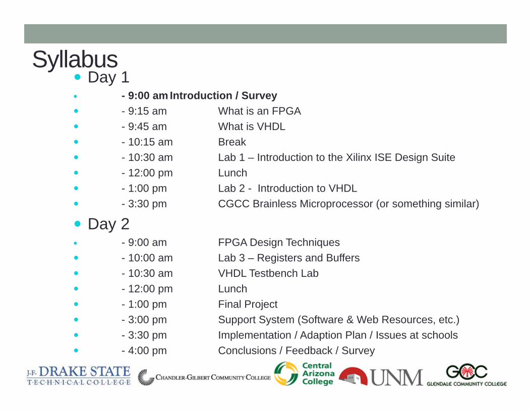
Syllabus Day 1 - 9:00 am Introduction / Survey - 9:15 am What is an FPGA - 9:45 am What is VHDL - 10:15 am Break - 10:30 am Lab 1 – Introduction to the Xilinx ISE Design Suite - 12:00 pm Lunch - 1:00 pm Lab 2 - Introduction to VHDL - 3:30 pm CGCC Brainless Microprocessor (or something similar)
Day 2 - 9:00 am FPGA Design Techniques - 10:00 am Lab 3 – Registers and Buffers - 10:30 am VHDL Testbench Lab - 12:00 pm Lunch - 1:00 pm Final Project - 3:00 pm Support System (Software & Web Resources, etc.) - 3:30 pm Implementation / Adaption Plan / Issues at schools - 4:00 pm Conclusions / Feedback / Survey

Why we are here
The average instructor when they are told they should be updating their digital logic lab by a department chair

The Big Picture

Technologies in My Lifetime
Application Specific Processors
Technology Gates Tools Processors Languages Focus
1960's Transistors 101
1970's SSI (7400) 102 8‐bit Fortran Algorithms
1980's PALs (22V10) 103 Scripting 16‐bit Pascal Data Structures
1990's CPLDs 104 Schematic Capture 32‐bit C, C+ Objects
2000's FPGAs 106 HDL, synth, analysis Multi‐core C++, Java Threads, Networks
2010's SOCs 109 HLSTs, IP, Cores SOCs C/HDLs? Partitioning, synching
Human Bandwidth Exceeded: Behavioral Design Human Ingenuity Challenged: CAD Tool Lag
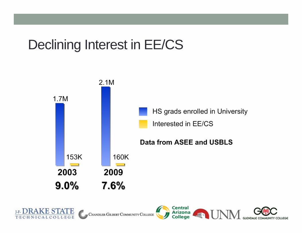
Declining Interest in EE/CS

Declining Enrollments and Graduates in EE/CS

We have the hardware, but…
“… the semiconductor industry threw the equivalent of a Hail Mary pass when it switched from making microprocessors run faster to putting more of them on a chip - doing so without any clear notion of how such devices would in general be programmed.
“The hope is that someone will be able to figure out how to do that, but at the moment, the ball is still in the air.”
“Chipmakers are busy designing microprocessors that most programmers can’t program”
David Patterson, IEEE Spectrum 2010
Courtesy Patrick Lysaght, Xilinx

65nm 40/45nm 28nm
200K
400K
600K
Logic Cells
800K
1,000K
332K
150K
760K
355K 410KVi
rtex
-7
Virt
ex-6
Spartan-6
Virt
ex-5
Dramatic Capacity Increases
Art
ix-7
2,000K
Kin
tex-
7
Courtesy Patrick Lysaght, Xilinx
Exponential Growth!

Students learn more, faster, and better with unrestricted access to design tools…
…overall learning improves when applied design skills taught early;
…overall performance improves when design skills used frequently;
…and they like it*
*results published in 2008 and 2009 ASEE proceedings
I never teach my pupils; I only attempt to provide the conditions in which they can learn. Albert Einstein
Method: Immersive hands-on design for every student

Low-cost kits and Free CAD tools for every engineering student
Terasic DE0Altera Cyclone III
$79
Terasic DE1Altera Cyclone II
$125
Digilent Basys2Xilinx Spartan 3E
$59
Digilent Nexys2Xilinx Spartan 3E
$99
No Lab Required! Students work on real designs at a time and place of their choosing

FPGA’s Across the Curriculum

Please interrupt and ask questions

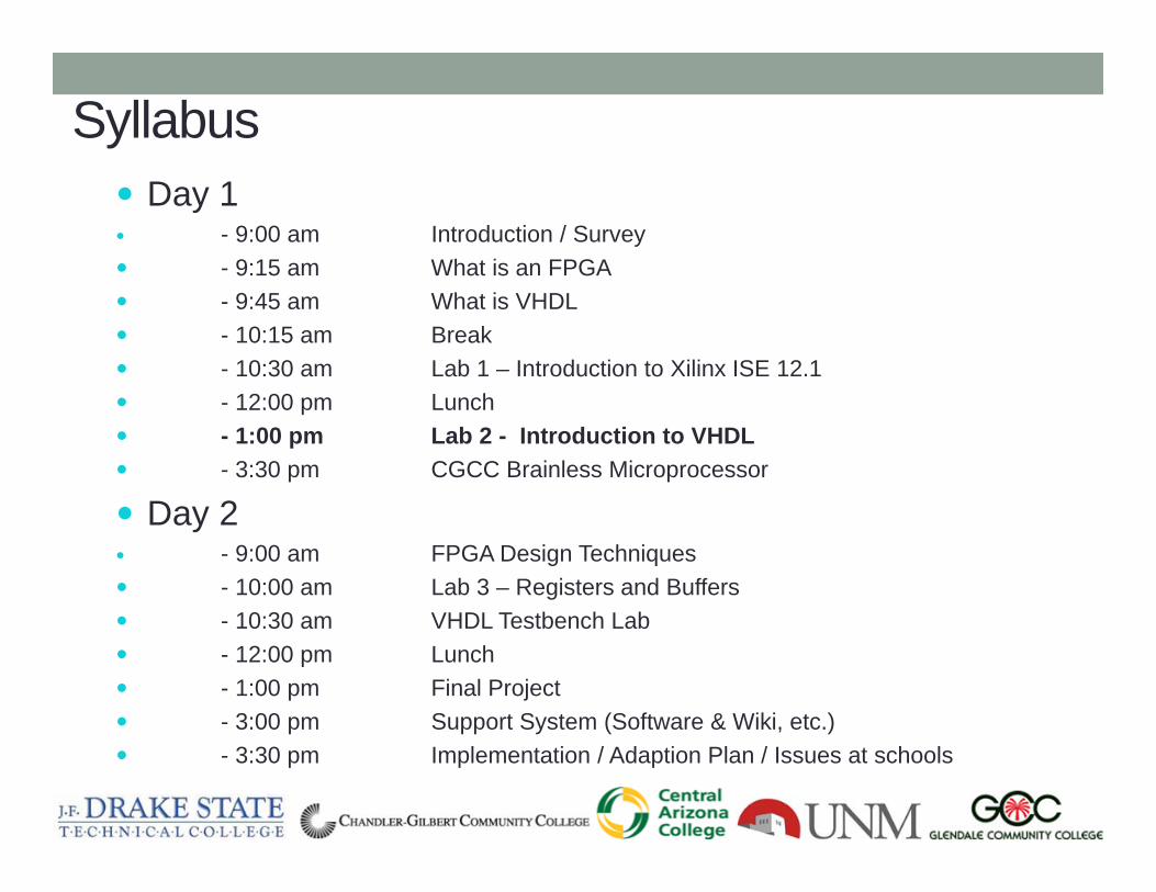
Syllabus Day 1 - 9:00 am Introduction / Survey - 9:15 am What is an FPGA - 9:45 am What is VHDL - 10:15 am Break - 10:30 am Lab 1 – Introduction to Xilinx ISE 12.1 - 12:00 pm Lunch - 1:00 pm Lab 2 - Introduction to VHDL - 3:30 pm CGCC Brainless Microprocessor
Day 2 - 9:00 am FPGA Design Techniques - 10:00 am Lab 3 – Registers and Buffers - 10:30 am VHDL Testbench Lab - 12:00 pm Lunch - 1:00 pm Final Project - 3:00 pm Support System (Software & Wiki, etc.) - 3:30 pm Implementation / Adaption Plan / Issues at schools - 4:00 pm Conclusions / Feedback / Survey

What is an FPGA• A Field Programmable Gate Array (FPGA) is a semiconductor device
containing programmable logic components and programmable interconnects. The programmable logic components can be programmed to duplicate the functionality of basic logic gates such as AND, OR, XOR, NOT or more complex combinatorial functions such as decoders or simple math functions. In most FPGAs, these programmable logic components also include memory elements, which may be simple flip-flops or complete blocks of memory.
• A hierarchy of programmable interconnects allows the logic blocks of an FPGA to be interconnected as needed by the system designer. These logic blocks and interconnects can be programmed after the manufacturing process by the customer so that the FPGA can perform whatever logical function that is needed.
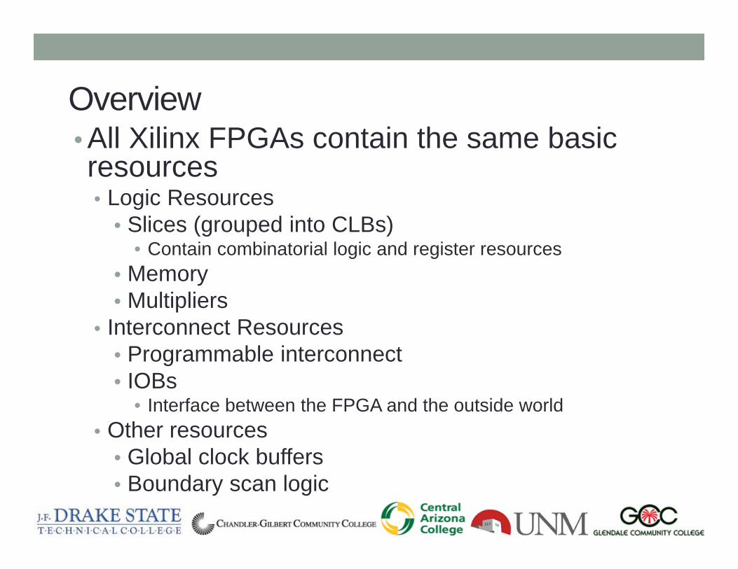
Overview• All Xilinx FPGAs contain the same basic resources• Logic Resources
• Slices (grouped into CLBs)• Contain combinatorial logic and register resources
• Memory• Multipliers
• Interconnect Resources• Programmable interconnect • IOBs
• Interface between the FPGA and the outside world• Other resources
• Global clock buffers• Boundary scan logic

What makes up an FPGA?
Groups of Slices make up a Complex Logic Block (CLB)
Each slice has four outputsTwo registered outputs, two non-registered outputs
Slice 0
LUTLUT CarryCarry
LUTLUT CarryCarry D QCE
PRE
CLR
DQCE
PRE
CLR
Simplified Slice Structure

Spartan-3E Architecture
CLB
Slice

Xilinx vs. Altera
• Make Hardware• Make Design Tools• What is the difference?

• It depends• Time• Existing resources• Money • Level of effort
Which is best?

What projects are FPGAs good for Aerospace & Defense
Radiation-tolerant FPGAs along with intellectual property for image processing, waveform generation, and partial reconfiguration for SDRs.
AutomotiveAutomotive silicon and IP solutions for gateway and driver assistance systems, comfort, convenience, and in-vehicle infotainment.
BroadcastSolutions enabling a vast array of broadcast chain tasks as video and audio finds its way from the studio to production and transmission and then to the consumer.
ConsumerCost-effective solutions enabling next generation, full-featured consumer applications, such as converged handsets, digital flat panel displays, information appliances, home networking, and residential set top boxes.
Industrial/Scientific/MedicalIndustry-compliant solutions addressing market-specific needs and challenges in industrial automation, motor control, and high-end medical imaging.
Storage & ServerData processing solutions for Network Attached Storage (NAS), Storage Area Network (SAN), servers, storage appliances, and more.
Wireless CommunicationsRF, base band, connectivity, transport and networking solutions for wireless equipment, addressing standards such as WCDMA, HSDPA, WiMAX and others.

Who uses them?
• www.fpgajobs.com
• Even though most jobs listed are for Engineers, there is a pathway ahead for anyone with this knowledge
• The FPGA Technician – Craig’s view of life

Why are they important
• They have the ability to revolutionize the way that prototyping is done.
• Allows companies to get to market quicker and stay in market longer.
• Allows small companies to create systems normally reserved for larger companies.

Syllabus Day 1 - 9:00 am Introduction / Survey - 9:15 am What is an FPGA - 9:45 am What is VHDL - 10:15 am Break - 10:30 am Lab 1 – Introduction to Xilinx ISE 12.1 - 12:00 pm Lunch - 1:00 pm Lab 2 - Introduction to VHDL - 3:30 pm CGCC Brainless Microprocessor
Day 2 - 9:00 am FPGA Design Techniques - 10:00 am Lab 3 – Registers and Buffers - 10:30 am VHDL Testbench Lab - 12:00 pm Lunch - 1:00 pm Final Project - 3:00 pm Support System (Software & Wiki, etc.) - 3:30 pm Implementation / Adaption Plan / Issues at schools - 4:00 pm Conclusions / Feedback / Survey
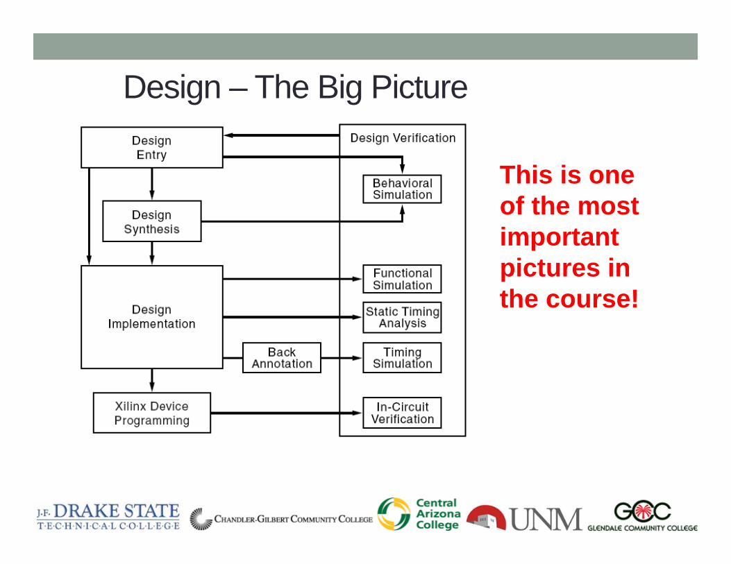
Design – The Big Picture
This is one of the most important pictures in the course!

This is the other!DESIGN
Hardware Descriptive Languages (HDL)
VHDLVERILOG
C++SYSGENSchematic CaptureEDKIP Cores
Limitless Tools
SYNTHESIS
Many files in – one file out
One File = EDIF
Syntax Checking
Less Tool Choices
IMPLEMENTATIONPLACE AND
ROUTE
Place Logic onto the CLBs
RouteIOB CLB IOB
UCFEDIF .BIT
ONE TOOL
PROGRAM
JTAG
PROGRAM
FPGA
PROM
ADEPT vs JTAG Chain
BEHAVIORAL SIMULATION TIMING SIMULATION

How are FPGA projects Designed?
• There are many different methodolgies for programming (or designing) with FPGAs• Hardware Descriptive Language (HDL)
• VHDL• Verilog
• Schematic Capture• C Code• EDK• System Generator

HDLs: VHDL and Verilog
• Hardware Descriptive Languages are ways of describing digital logic. They are not a programming language, they are languages for describing hardware and are the most popular mechanisms for creating FPGA projects• VHDL – VHSIC Hardware Descriptive Language• Verilog
• Which is best?
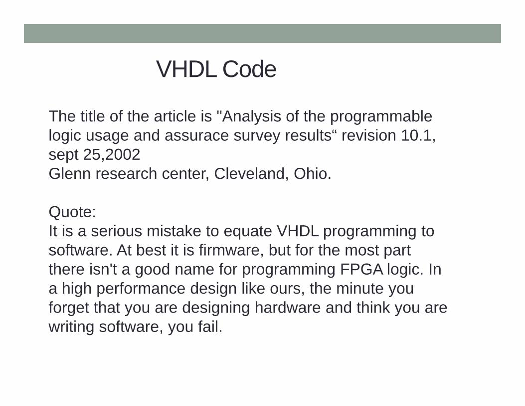
VHDL Code
The title of the article is "Analysis of the programmable logic usage and assurace survey results“ revision 10.1, sept 25,2002Glenn research center, Cleveland, Ohio.
Quote:It is a serious mistake to equate VHDL programming to software. At best it is firmware, but for the most part there isn't a good name for programming FPGA logic. In a high performance design like ours, the minute you forget that you are designing hardware and think you are writing software, you fail.

Synthesizable vs. Non-Synthesizable VHDL Code
Forest Level View on Synthesizable Code

• Inputs and outputs for FPGA
• std_logic versus std_logic_vector
• -- comments: how you enter comments in VHDL
entity BUZZER is port (
DOOR, IGNITION, SBELT: in std_logic;
WARNING: out std_logic);
end BUZZER;
Entity Declaration
DOOR
IGNITION
SBELT
WARNING
entity BUZZER is port (
DOOR: in std_logic;
IGNITION: in std_logic;
SBELT: in std_logic;
WARNING: out std_logic);
end BUZZER;
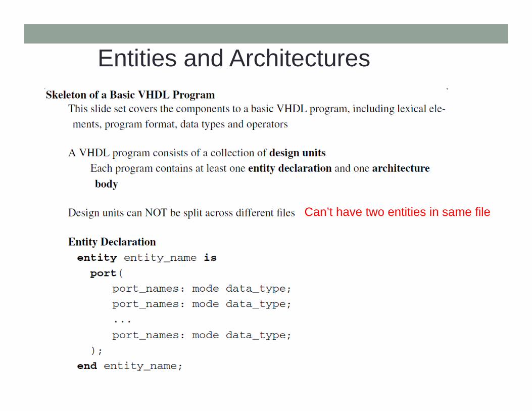
Entities and Architectures
Can’t have two entities in same file

Signals – Internal to one source file
• Inside architecture and before the “begin”• Think of as a temporary value• Can’t be seen outside of the file• If you want to simulate, drive the output to an I/O pin
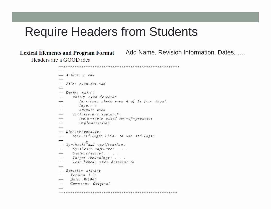
Require Headers from StudentsAdd Name, Revision Information, Dates, ….

Complete VHDL project

Syllabus Day 1 - 9:00 am Introduction / Survey - 9:15 am What is an FPGA - 9:45 am What is VHDL - 10:15 am Break - 10:30 am Lab 1 – Introduction to Xilinx ISE 12.1 - 12:00 pm Lunch - 1:00 pm Lab 2 - Introduction to VHDL - 3:30 pm CGCC Brainless Microprocessor
Day 2 - 9:00 am FPGA Design Techniques - 10:00 am Lab 3 – Registers and Buffers - 10:30 am VHDL Testbench Lab - 12:00 pm Lunch - 1:00 pm Final Project - 3:00 pm Support System (Software & Wiki, etc.) - 3:30 pm Implementation / Adaption Plan / Issues at schools - 4:00 pm Conclusions / Feedback / Survey

Syllabus Day 1 - 9:00 am Introduction / Survey - 9:15 am What is an FPGA - 9:45 am What is VHDL - 10:15 am Break - 10:30 am Lab 1 – Introduction to the Xilinx ISE Design Environment - 12:00 pm Lunch - 1:00 pm Lab 2 - Introduction to VHDL - 3:30 pm CGCC Brainless Microprocessor
Day 2 - 9:00 am FPGA Design Techniques - 10:00 am Lab 3 – Registers and Buffers - 10:30 am VHDL Testbench Lab - 12:00 pm Lunch - 1:00 pm Final Project - 3:00 pm Support System (Software & Wiki, etc.) - 3:30 pm Implementation / Adaption Plan / Issues at schools - 4:00 pm Conclusions / Feedback / Survey

I wish to help all of you to begin teaching FPGAs

Lab 1 Overview
• Provides you with an introduction to the design tools with a schematic capture environment
• I will show you how to do a simple schematic project and you can follow the instructions later to repeat after lunch
Start the Learning
The key from this workshop is to learn what you need to know to successfully teach with FPGAs

Syllabus Day 1 - 9:00 am Introduction / Survey - 9:15 am What is an FPGA - 9:45 am What is VHDL - 10:15 am Break - 10:30 am Lab 1 – Introduction to Xilinx ISE 12.1 - 12:00 pm Lunch and Talking ATE - 1:00 pm Lab 2 - Introduction to VHDL - 3:30 pm CGCC Brainless Microprocessor
Day 2 - 9:00 am FPGA Design Techniques - 10:00 am Lab 3 – Registers and Buffers - 10:30 am VHDL Testbench Lab - 12:00 pm Lunch - 1:00 pm Final Project - 3:00 pm Support System (Software & Wiki, etc.) - 3:30 pm Implementation / Adaption Plan / Issues at schools

Advanced Technological Education (ATE)
Synopsis of Program:With an emphasis on two-year colleges, the Advanced Technological Education (ATE) program focuses on the education of technicians for the high-technology fields that drive our nation's economy. The program involves partnerships between academic institutions and employers to promote improvement in the education of science and engineering technicians at the undergraduate and secondary school levels. The ATE program supports curriculum development; professional development of college faculty and secondary school teachers; career pathways to two-year colleges from secondary schools and from two-year colleges to four-year institutions; and other activities. Another goal is articulation between two-year and four-year programs for K-12 prospective teachers that focus on technological education. The program also invites proposals focusing on research to advance the knowledge base related to technician education.

ATE VideoWhat is ATE? Video

Advanced Technological Education (ATE)Cognizant Program Officer(s):Please note that the following information is current at the time of publishing. See program website for any updates to the points ofcontact.V. Celeste Carter, Lead Program Director, 835 N, telephone: (703) 292-4651, email: [email protected]
Gerhard L. Salinger, Lead Program Director, DRL, 885 S, telephone: (703) 292-5116, email: [email protected]
David B. Campbell, Co-Lead Program Director, DRL, 885 S, telephone: (703) 292-5093, email: [email protected]
Pamela Brown, 835 N, telephone: (703) 292-4674, email: [email protected]
Zhanjing (John) Yu, 835 S, telephone: (703) 292-4647, email: [email protected]

Advanced Technological Education (ATE)
Synopsis of Program:With an emphasis on two-year colleges, the Advanced Technological Education (ATE) program focuses on the education of technicians for the high-technology fields that drive our nation's economy. The program involves partnerships between academic institutions and employers to promote improvement in the education of science and engineering technicians at the undergraduate and secondary school levels. The ATE program supports curriculum development; professional development of college faculty and secondary school teachers; career pathways to two-year colleges from secondary schools and from two-year colleges to four-year institutions; and other activities. Another goal is articulation between two-year and four-year programs for K-12 prospective teachers that focus on technological education. The program also invites proposals focusing on research to advance the knowledge base related to technician education.

Anticipated number, size, and duration of new awards
- ATE Projects: approximately 45-60 new awards, ranging from $25,000 to $300,000 per year and having a duration of up to three years, except for Large Scale Materials Development (LSMD) projects, which are limited to $500,000 per year for four years.- ATE small grants for institutions new to the ATE program: approximately 15-20 awards for up to $200,000 (each) typically spread over three years. It is expected that the budget request will match the scope of the project.- National Centers of Excellence: up to 2 new awards for up to $5 million (each) spread over four years, with the possibility of a competitive grant renewal, normally at a lower level of annual funding, for an additional three years.- Regional Centers of Excellence: up to 3 new awards for up to $3 million (each) spread over four years, with the possibility of a competitive grant renewal, normally at a lower level of annual funding, for an additional three years.- Resource Centers: up to 4 new awards for up to $1.6 million (each) spread over four years with the possibility of a competitive grant renewal.- Planning Grants for Centers: up to 4 new awards for up to $70,000 (each) to develop well-formulated plans for future national or regional centers (see Section V.A ["Proposal Preparation"] for additional information).- Targeted Research on Technician Education: approximately 5 to 8 new awards, ranging from $100,000 to $300,000 per year for up to 4 years.

Tips and Tricks• Read the solicitation• Talk to the NSF PM about your ideas• Have a half dozen “measurable” goals• Have a good external evaluator• Start early. Proposals are always due in October. Starting
six months out is not to early• Success means clearly showing with supporting
documentation• What you want to do• Why you want to do it• Who cares
Syllabus Day 1 - 9:00 am Introduction / Survey - 9:15 am What is an FPGA - 9:45 am What is VHDL - 10:15 am Break - 10:30 am Lab 1 – Introduction to Xilinx ISE 12.1 - 12:00 pm Lunch - 1:00 pm Lab 2 - Introduction to VHDL - 3:30 pm CGCC Brainless Microprocessor
Day 2 - 9:00 am FPGA Design Techniques - 10:00 am Lab 3 – Registers and Buffers - 10:30 am VHDL Testbench Lab - 12:00 pm Lunch - 1:00 pm Final Project - 3:00 pm Support System (Software & Wiki, etc.) - 3:30 pm Implementation / Adaption Plan / Issues at schools

Lab 2 Overview
• Introduction to VHDL• Builds upon schematic capture skills but with an HDL• I will do a simple project first. You watch and then you can
follow the directions

Syllabus Day 1 - 9:00 am Introduction / Survey - 9:15 am What is an FPGA - 9:45 am What is VHDL - 10:15 am Break - 10:30 am Lab 1 – Introduction to Xilinx ISE 12.1 - 12:00 pm Lunch - 1:00 pm Lab 2 - Introduction to VHDL - 3:30 pm CGCC Brainless Microprocessor
Day 2 - 9:00 am FPGA Design Techniques - 10:00 am Lab 3 – Registers and Buffers - 10:30 am VHDL Testbench Lab - 12:00 pm Lunch - 1:00 pm Final Project - 3:00 pm Support System (Software & Wiki, etc.)

Day 2
• Recap yesterday events

Syllabus
Day 2 - 9:00 am FPGA Design Techniques - 10:00 am Lab 3 – Registers and Buffers - 10:30 am VHDL Testbench Lab - 12:00 pm Lunch - 1:00 pm Final Project - 3:00 pm Support System (Software & Wiki, etc.) - 3:30 pm Implementation / Adaption Plan / Issues at schools - 4:00 pm Conclusions / Feedback / Survey
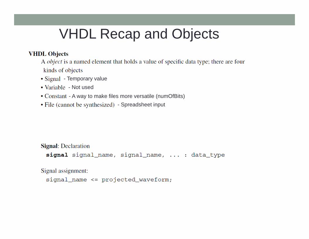
VHDL Recap and Objects
- Temporary value- Not used- A way to make files more versatile (numOfBits)
- Spreadsheet input
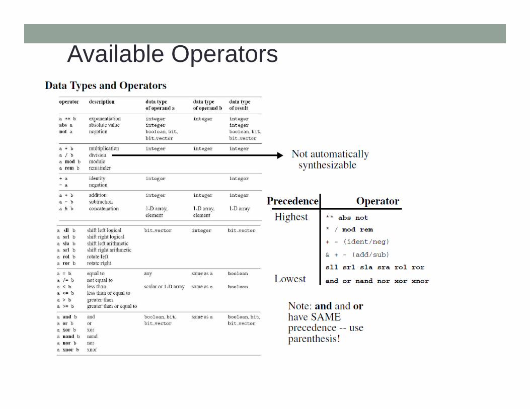
Available Operators

Picking off bits

CASE STATEMENT
SELECTED SIGNAL ASSIGNMENT
00011011
process(SEL, HEX0, HEX1, HEX2, HEX3)begincase SEL is
when "00" =>
AN <= "1110";HEX <= HEX0;
when "01" =>AN <= "1101";HEX <= HEX1;
when "10" =>AN <= "1011";HEX <= HEX2;
when others =>AN <= "0111";HEX <= HEX3;
end case;end process;
* USED WHEN NO PRIORITY EQUIVALENT TO CASE STATEMENT

IF STATEMENT
CONDITIONAL SIGNAL ASSIGNMENT PROCESS (X, Y, Z, A, B) SENSITIVITY LIST. ANYTHING READ MUST BE HERE NOTHING HERE IS EVER ON LEFT
SIDE OF ASSIGNMENT – Everything on Right hand side of assignment is read
01
IF B = ‘1’ THENOUT <= Z
ELSIF A = ‘1’OUT <= Y
ELSEOUT <= X
END IFEND
PROCESS* PRIORITY EXISTS
X
Y01
OUT
ZA
B
- no clock
Assignment Operators
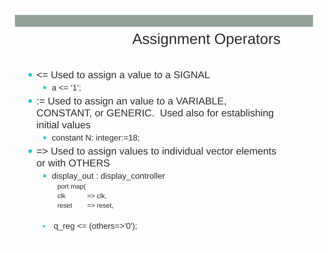
<= Used to assign a value to a SIGNAL a <= ‘1’;
:= Used to assign an value to a VARIABLE, CONSTANT, or GENERIC. Used also for establishing initial values constant N: integer:=18;
=> Used to assign values to individual vector elements or with OTHERS display_out : display_controller
port map(clk => clk, reset => reset,
• q_reg <= (others=>'0');

RULES1. DON’T USE PROCESS IF DON’T HAVE TO – Simple, concurrent and selected signal assignments can be done outside of a process. Danger of using a process is you might get a inferred latch (unwanted clock cycle)
2. MULTIPLE ASSIGNMENTS TO SAME SIGNAL, LAST ONE HOLDS:A <= ‘1’;A <= ‘0’;
3. FOR EVERY OUTPUT SIGNAL THAT CAN BE ASSIGNED, ALL POSSIBLE CONDITIONS MUST BE ADDRESSED– Always assign default values at the top of the block before case and if statements
4. ALL INPUT SIGNALS READ MUST BE IN THE SENSITIVITY LIST FOR COMBINATIONAL LOGIC
5. FOR SEQUENTIAL USE CLK/RESET
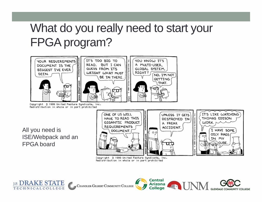
What do you really need to start your FPGA program?
All you need is ISE/Webpack and an FPGA board

Obtaining, licensing and service contract with Xilinx
• If you decide to go with Xilinx, we can help you the most (with currently available resources)• Register with XUP• Get software• Put one person in charge of licenses. Should be you. Don’t use your
normal password so you can easily share with your IT person

FPGA Project 101
• Every FPGA project has four steps• Design• Synthesis• Place and route• Program device• A good way to introduce
FPGA to your students

Entering Designs
Select source type• Design Entry
• Schematic• HDL source (VHDL and Verilog)
• Design Entry Tools• Architecture Wizard• Core Generator• Chipscope• State Diagram• Embedded Processor
• Simulation Test Bench• VHDL

Xilinx CORE Generator Predefined packages of VHDL optimized for a specific chip

Synthesis
• Synthesis is the process of combining all your design files into a single EDIF netlist. We use XST (Xilinx Synthesis Tool) for this purpose.
• There are other packages but at an educational level, it may not be fiscally prudent (or necessary).
Synthesis – Choosing space, speed and other options

Synthesizing Designs
Double‐click to SynthesizeSynthesis Processes and Analysis
• Access report• View Schematics (RTL or Technology)• Check syntax• Generate Post-Synthesis Simulation Model
Generate a netlist file using XST (Xilinx Synthesis Technology) Highlight HDL
Sources
1
2

RTL ViewerAllows designer to view schematic representation of the HDL.
Excellent troubleshooting tool

Implementing Designs
• Implement a design• Translate
• Access reports• Floorplan design
• Map• Access reports• Analyze timing• Floorplan design• Manually place components• Generate simulation model
• Place & Route• Access reports• Analyze timing• Floorplan design• Manually place & route components• And more
Process netlist generated from synthesis
Highlight HDLSources
1
Double‐click to Synthesize
2

Implementation Consists of three phases
Translate: Merge multiple design files into a single netlist
Map: Group logical symbols from the netlist (gates) into physical components (slices and IOBs)
Place & Route: Place components onto the chip, connect the components, and extract timing data into reports
Access Xilinx reports and tools at each phase Timing Analyzer, Floorplanner,
FPGA Editor, XPower
Translate
Map
Place & Route
Implement
. . .
. . .
Netlist GeneratedFrom Synthesis
. . .

Place and Route
• P&R is the process of translating the netlist into physical gates on the chip
• This is where you care about the specific chip you will be using and you will see the introduction of the UCF.
• The UCF is a user constraint file that ties your projects inputs and outputs to actual pins on the chip.

SynthesisSchematicCapture
Simulation0 1 0 0 1 1 1 0 1 1 0 0 1 1 1 1
Design Flow
libraries
netlist
HDL
test vectors
Translate
Fitting/Place & Route
Implementation
Specification
Verification
Gates of the design ...
... are placed ... ... and routed
Device Implementation Place & Route

Simulating Designs
Tool Flow 75
Verify the design with the ISE SimulatorSelect simulation type
1
Highlight test bench
2
Double‐click tosimulate
3
Add a test bench• VHDLPerform a Behavioral Simulation• Use UNISIM/UniMacro library when FPGA primitives
are instantiated in the design• Use XilinxCoreLib library when IP cores are
instantiated in the designPerform a timing simulation• Use Xilinx SIMPRIM library when FPGA primitives
are instantiated in the design SmartModels• Simulation library for both functional and timing simulation of Xilinx Hard-IP such as PPC, PCIe, GT, TEMAC.

Simulations
90% (maybe 100% at a 200 level course
10%

Counter Simulation
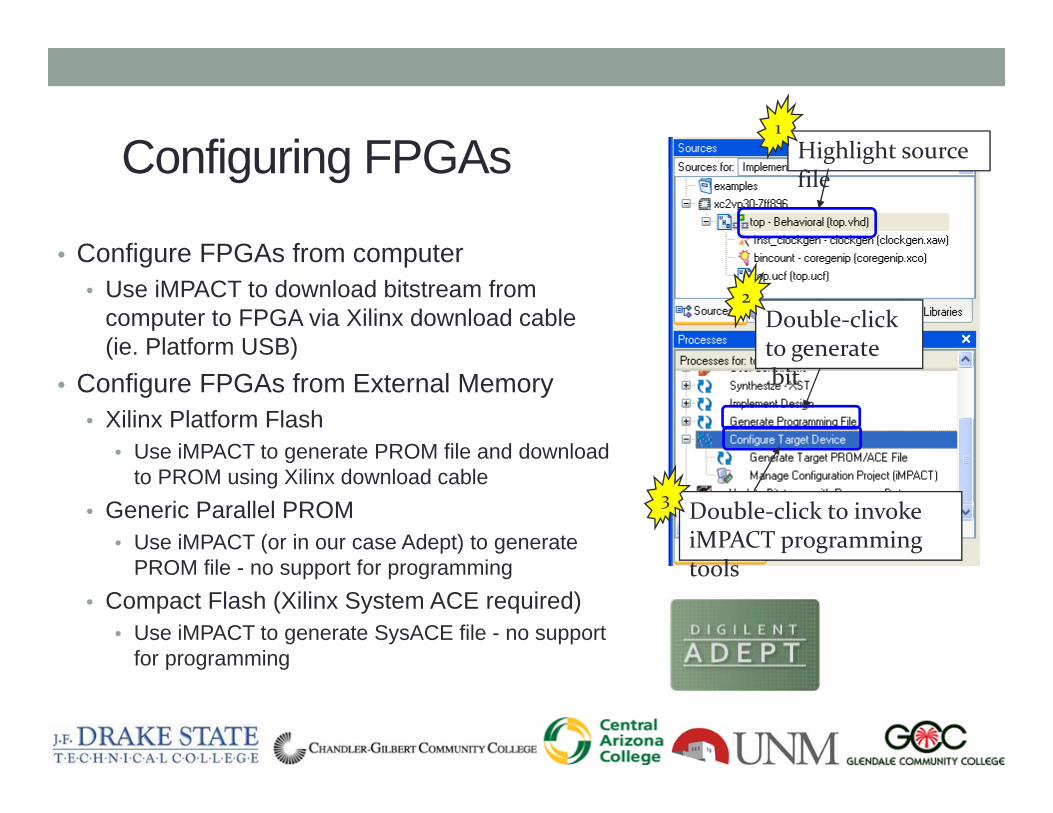
Configuring FPGAs
• Configure FPGAs from computer• Use iMPACT to download bitstream from
computer to FPGA via Xilinx download cable (ie. Platform USB)
• Configure FPGAs from External Memory• Xilinx Platform Flash
• Use iMPACT to generate PROM file and download to PROM using Xilinx download cable
• Generic Parallel PROM• Use iMPACT (or in our case Adept) to generate
PROM file - no support for programming• Compact Flash (Xilinx System ACE required)
• Use iMPACT to generate SysACE file - no support for programming
Double‐click to generate .bit
2
Highlight source file
1
Double‐click to invoke iMPACT programming tools
3

Configuration • Once a design is implemented, you must create a file that
the FPGA can understand• This file is called a bitstream: a BIT file (.bit extension)
• The BIT file can be downloaded • Directly into the FPGA
• Use a download cable such as Platform USB• To external memory device such as a Xilinx Platform Flash PROM
• Must first be converted into a PROM file
Tool Flow 79

Syllabus
Day 2 - 9:00 am FPGA Design Techniques - 10:00 am Lab 3 – Registers and Buffers - 10:30 am VHDL Testbench Lab - 12:00 pm Lunch - 1:00 pm Final Project - 3:00 pm Support System (Software & Wiki, etc.) - 3:30 pm Implementation / Adaption Plan / Issues at schools - 4:00 pm Conclusions / Feedback / Survey
Lab 3
• Difference between a register and a buffer• Do the lab
Syllabus
Day 2 - 9:00 am FPGA Design Techniques - 10:00 am Lab 3 – Registers and Buffers - 10:30 am VHDL Testbench Lab - 12:00 pm Lunch - 1:00 pm Final Project - 3:00 pm Support System (Software & Wiki, etc.) - 3:30 pm Implementation / Adaption Plan / Issues at schools - 4:00 pm Conclusions / Feedback / Survey

Don’t get frustrated
The project may not be successful for each person the first time. Don’t get frustrated. The process is simple but it is often easy to make simple mistakes the first time you do this.

VHDL Testbench Lab
• Could this be a now position for a technician or a two year degree person?
• Go through the Counter Code
Syllabus
Day 2 - 9:00 am FPGA Design Techniques - 10:00 am Lab 3 – Registers and Buffers - 10:30 am VHDL Testbench Lab - 12:00 pm Lunch - 1:00 pm Final Project - 3:00 pm Support System (Software & Wiki, etc.) - 3:30 pm Implementation / Adaption Plan / Issues at schools - 4:00 pm Conclusions / Feedback / Survey

Final Project

Syllabus Day 2 - 9:00 am FPGA Design Techniques - 10:00 am Lab 3 – Registers and Buffers - 10:30 am VHDL Testbench Lab - 12:00 pm Lunch - 1:00 pm Final Project - 3:00 pm Support System (Software & Web Resources, etc.) - 3:30 pm Implementation / Adaption Plan / Issues at schools - 4:00 pm Conclusions / Feedback / Survey

Webpack
This is the really great benefit to students. Xilinx makes a free version of their ISE software. This means that students can do entire projects at home and only come to the lab to demo.
http://www.xilinx.com/ise/logic_design_prod/webpack.htm
Altera has a similar product

Webpack

Webpack vs Full Version

Default Locations for SW
• When you are setting up the software, regardless of if it is at the lab or at home, only install the software at the default locations.

Prototype Boards
• Boards range from very inexpensive (BASYX - $59) to very expensive (V8000 - $10k). They key is to get the most board you can for the minimum amount of money that will do what you need.
• Excellent dependability and student tested.• Clint Cole story• Clint’s website – www.digilentinc.com
Licensing
• Node Lock (Ethernet versus Hard Drive Serial Number)• Server Licensing• Student versus Lab• Let us work with your IT folks. This part gets confusing
quickly your first few times.

License Donation according to XUP
• All of the seats/licenses come with 1yr warrantee/maintenance. The software and licenses do not expire nor do they stop working. The current software version installation can be used for as long as needed, these are perpetual licenses. What does expire is the warrantee/maintenance on the tools. This means you will not receive any NEW software versions/updates.
• To stay in warrantee the school must complete and submit the on-line donation request located at http://www.xilinx.com/university/donation/index.htm and request what software they want. Once the request is received an order is placed. This will extend SW access for 1 more year and assure no lapse in receiving all updates/new software versions.

Digilent (cont.)
• Clint’s boards, website and PMODs

Educational Materials Available
• Clint’s web site www.eecs.wsu.edu/~ee214• Digilent website www.digilentinc.com• Our XUP site www.ece.unm.edu/vhdl• XUP site• www.cosmiac.org• Quick start tutorials – launch within ISE• What we are developing!

Deploying Curriculum
• Website: http://cosmiac.org/FPGA.html

Educational Materials Available
http://www.digilentinc.com/classroom/realdigital/

Educational Materials Availablehttp://www.cosmiac.org/spartan3e_tutorials.html

Free Textbook• http://www.allaboutcircuits.com/

Donated SW and HW
• Register with XUP• Mention working with us• Don’t chase releases• What is “good enough”
• Computers• Software/releases OS/ISE• Boards
• HW• Initially• Sporadic• Sustainability

Impediments to Implementation
• Hurdles we have seen• We have always done it this way
• Hurdles you might see• Fear factor
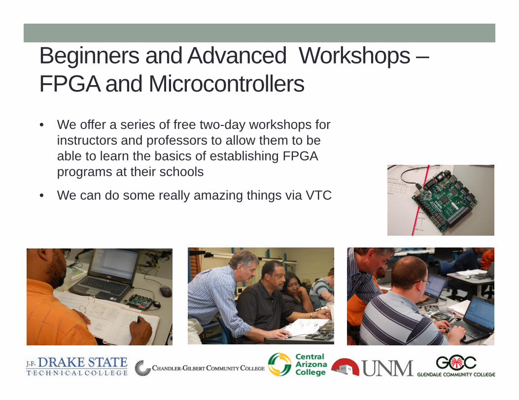
Beginners and Advanced Workshops –FPGA and Microcontrollers• We offer a series of free two-day workshops for
instructors and professors to allow them to be able to learn the basics of establishing FPGA programs at their schools
• We can do some really amazing things via VTC

The Team’s Plan
• Develop Instructional Material• Train Faculty

Collaboration• We do
collaborations very well
• Small Grants for Institutions New to the ATE Program
• Project Proposals

Developing Curriculum
• Lab1 – Intro - Matar/Luu• Lab 2 – Basic Logic Gates Matar/Luu• Lab 3 – Registers and Buffers Kief• Lab 4 – Simulation (tie to Lab 7 & 8) Henry/Reutter• Lab 5 – Look-up Tables Kief• Lab 6 – ALU Matar/Luu• Lab 7 – Test Bench 1 Henry/Reutter• Lab 8 –Troubleshooting Henry/Reutter• Lab 9 – Counters Kief• Lab 10 – Finite State Machines Matar/Luu• Lab 11 – Sequence Detectors Henry/Reutter• Lab 12 – Shift Registers Kief• Lab 13 – IP Cores Kief• Lab 14 – Microprocessor System Lomeli• Lab 15 – Chipscope Pro Lomeli• Lab 16 – RS-232 & Series Communication Kief

Plan Ahead
• In the near future Xilinx ISE will transition from the traditional Project Navigator to Plan Ahead.
• Easier integration of various design types

PlanAhead
• Very similar to project navigator

Teaching Faculty
• Lets do an Advanced Workshop

Syllabus
Day 2 - 9:00 am FPGA Design Techniques - 10:00 am Lab 3 – Registers and Buffers - 10:30 am VHDL Testbench Lab - 12:00 pm Lunch - 1:00 pm Final Project - 3:00 pm Support System (Software & Wiki, etc.) - 3:30 pm Implementation / Adaption Plan / Issues at schools - 4:00 pm Conclusions / Feedback / Survey

Conclusions

Painful survey
We need your help in statistics. We will be contacting you!