free datasheet search enginedatasheet.buhieen.net/lf13331m.pdf · tain a constant resistance over...
TRANSCRIPT
LF11331/LF13331/LF11332/LF13332/LF11333/LF13333/LF11201/LF13201/LF11202/LF13202Quad SPST JFET Analog SwitchesGeneral DescriptionThese devices are a monolithic combination of bipolar andJFET technology producing the industry’s first one chip quadJFET switch. A unique circuit technique is employed to main-tain a constant resistance over the analog voltage range of±10V. The input is designed to operate from minimum TTLlevels, and switch operation also ensures abreak-before-make action.
These devices operate from ±15V supplies and swing a±10V analog signal. The JFET switches are designed for ap-plications where a dc to medium frequency analog signalneeds to be controlled.
Featuresn Analog signals are not loadedn Constant “ON” resistance for signals up to ±10V and
100 kHzn Pin compatible with CMOS switches with the advantage
of blow out free handlingn Small signal analog signals to 50 MHzn Break-before-make action: tOFF < tON
n High open switch isolation at 1.0 MHz: −50 dBn Low leakage in “OFF” state: <1.0 nAn TTL, DTL, RTL compatibilityn Single disable pin opens all switches in package on
LF11331, LF11332, LF11333n LF11201 is pin compatible with DG201
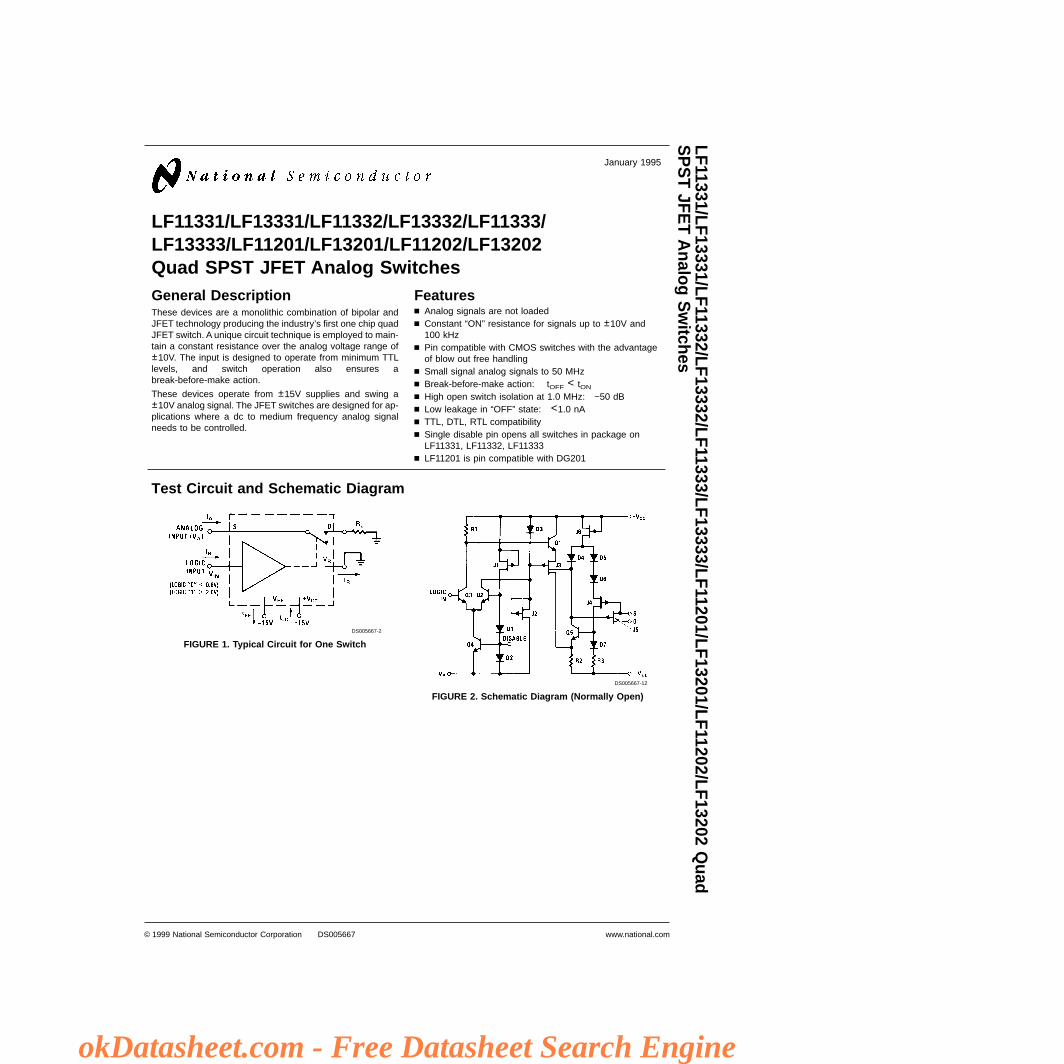
Test Circuit and Schematic Diagram
DS005667-2
FIGURE 1. Typical Circuit for One Switch
DS005667-12
FIGURE 2. Schematic Diagram (Normally Open)
January 1995
LF11331/LF13331/LF11332/LF13332/LF11333/LF13333/LF11201/LF13201/LF11202/LF13202Q
uadS
PS
TJFE
TA
nalogS
witches
© 1999 National Semiconductor Corporation DS005667 www.national.com
okDatasheet.com - Free Datasheet Search Engine

Absolute Maximum Ratings (Note 1)
If Military/Aerospace specified devices are required,please contact the National Semiconductor Sales Office/Distributors for availability and specifications.
(Note 2)
Supply Voltage (VCC−VEE) 36VReference Voltage VEE≤VR≤VCC
Logic Input Voltage VR−4.0V≤VIN≤VR+6.0VAnalog Voltage VEE≤VA≤VCC+6V;
VA≤VEE+36VAnalog Current |IA|<20 mA
Power Dissipation (Note 3)Molded DIP (N Suffix) 500 mWCavity DIP (D Suffix) 900 mW
Operating Temperature RangeLF11201, 2 and LF11331, 2, 3 −55˚C to +125˚CLF13201, 2 and LF13331, 2, 3 0˚C to +70˚C
Storage Temperature −65˚C to +150˚CSoldering Information
N and D Package (10 sec.) 300˚CSO Package:
Vapor Phase (60 sec.) 215˚CInfrared (15 sec.) 220˚C
Electrical Characteristics (Note 4)
LF11331/2/3 LF13331/2/3
Symbol Parameter Conditions LF11201/2 LF13201/2 Units
Min Typ Max Min Typ Max
RON “ON” Resistance VA=0, ID=1 mA TA=25˚C 150 200 150 250 Ω
200 300 200 350 Ω
RON Match “ON” Resistance Matching TA=25˚C 5 20 10 50 Ω
VA Analog Range ±10 ±11 ±10 ±11 V
IS(ON) + Leakage Current in “ON” Condition Switch “ON,” VS=VD=±10V TA=25˚C 0.3 5 0.3 10 nA
ID(ON) 3 100 3 30 nA
IS(OFF) Source Current in “OFF” Condition Switch “OFF,” VS=+10V, TA=25˚C 0.4 5 0.4 10 nA
VD=−10V 3 100 3 30 nA
ID(OFF) Drain Current in “OFF” Condition Switch “OFF,” VS=+10V, TA=25˚C 0.1 5 0.1 10 nA
VD=−10V 3 100 3 30 nA
VINH Logical “1” Input Voltage 2.0 2.0 V
VINL Logical “0” Input Voltage 0.8 0.8 V
IINH Logical “1” Input Current VIN=5V TA=25˚C 3.6 1025
3.6 40100 µA
IINL Logical “0” Input Current VIN=0.8 TA=25˚C 0.1 0.1 µA
1 1 µA
tON Delay Time “ON” VS=±10V, (Figure 3) TA=25˚C 500 500 ns
tOFF Delay Time “OFF” VS=±10V, (Figure 3) TA=25˚C 90 90 ns
tON−tOFF Break-Before-Make VS=±10V, (Figure 3) TA=25˚C 80 80 ns
CS(OFF) Source Capacitance Switch “OFF,” VS=±10V TA=25˚C 4.0 4.0 pF
CD(OFF) Drain Capacitance Switch “OFF,” VD=±10V TA=25˚C 3.0 3.0 pF
CS(ON) + Active Source and Drain Capacitance Switch “ON,” VS=VD=0V TA=25˚C 5.0 5.0 pF
CD(ON)
ISO(OFF) “OFF” Isolation (Figure 4), (Note 5) TA=25˚C −50 −50 dB
CT Crosstalk (Figure 4), (Note 5) TA=25˚C −65 −65 dB
SR Analog Slew Rate (Note 6) TA=25˚C 50 50 V/µs
IDIS Disable Current (Figure 5), (Note 7) TA=25˚C 0.4 1.0 0.6 1.5 mA
0.6 1.5 0.9 2.3 mA
IEE Negative Supply Current All Switches “OFF,” VS=±10V TA=25˚C 3.0 5.0 4.3 7.0 mA
4.2 7.5 6.0 10.5 mA
IR Reference Supply Current All Switches “OFF,” VS=±10V TA=25˚C 2.0 4.0 2.7 5.0 mA
2.8 6.0 3.8 7.5 mA
ICC Positive Supply Current All Switches “OFF,” VS=±10V TA=25˚C 4.5 6.0 7.0 9.0 mA
6.3 9.0 9.8 13.5 mA
Note 1: “Absolute Maximum Ratings” indicate limits beyond which damage to the device may occur. Operating Ratings indicate conditions for which the device isfunctional, but do not guarantee specific performance limits.
Note 2: Refer to RETSF11201X, RETSF11331X, RETSF11332X and RETSF11333X for military specifications.
Note 3: For operating at high temperature the molded DIP products must be derated based on a +100˚C maximum junction temperature and a thermal resistanceof +150˚C/W, devices in the cavity DIP are based on a +150˚C maximum junction temperature and are derated at ±100˚C/W.
www.national.com 2
okDatasheet.com - Free Datasheet Search Engine

Electrical Characteristics (Note 4) (Continued)
Note 4: Unless otherwise specified, VCC=+15V, VEE=−15V, VR=0V, and limits apply for −55˚C≤TA≤+125˚C for the LF11331/2/3 and the LF11201/2,−25˚C≤TA≤+85˚C for the LF13331/2/3 and the LF13201/2.
Note 5: These parameters are limited by the pin to pin capacitance of the package.
Note 6: This is the analog signal slew rate above which the signal is distorted as a result of finite internal slew rates.
Note 7: All switches in the device are turned “OFF” by saturating a transistor at the disable node as shown in Figure 5. The delay time will be approximately equalto the tON or tOFF plus the delay introduced by the external transistor.
Note 8: This graph indicates the analog current at which 1% of the analog current is lost when the drain is positive with respect to the source.
Note 9: θJA (Typical) Thermal Resistance
Molded DIP (N) 85˚C/W
Cavity DIP (D) 100˚C/W
Small Outline (M) 105˚C/W
Connection Diagrams (Top View for SO and Dual-In-Line Packages) (All Switches Shown are For Logical “0”)
LF11331/LF13331
DS005667-1
LF11332/LF13332
DS005667-13
LF11333/LF13333
DS005667-14
LF11201/LF13201
DS005667-15
www.national.com3
okDatasheet.com - Free Datasheet Search Engine

Connection Diagrams (Top View for SO and Dual-In-Line Packages) (All Switches Shown are For Logical“0”) (Continued)
LF11202/LF13202
DS005667-16
Order Number LF13201D, LF11201D, LF11201D/883, LF13202D, LF11202D, LF11202D/883, LF13331D, LF11331D,LF11331D/883, LF13332D, LF11332D, LF11332D/883, LF13333D, LF11333D or LH11333D/883
See NS Package Number D16COrder Number LF13201M, LF13202M, LF13331M, LF13332M or LF13333M
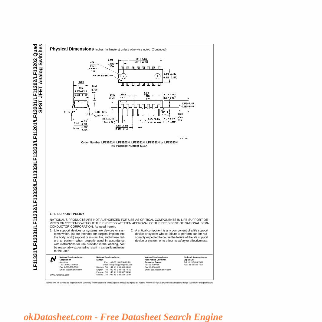
See NS Package Number M16AOrder Number LF13201N, LF13202N, LF13331N, LF13332N or LF13333N
See NS Package Number N16A
www.national.com 4
okDatasheet.com - Free Datasheet Search Engine
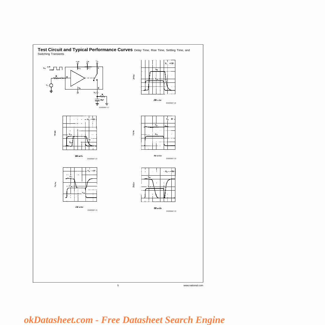
Test Circuit and Typical Performance Curves Delay Time, Rise Time, Settling Time, andSwitching Transients
DS005667-17
DS005667-18
DS005667-19 DS005667-20
DS005667-21DS005667-22
www.national.com5
okDatasheet.com - Free Datasheet Search Engine
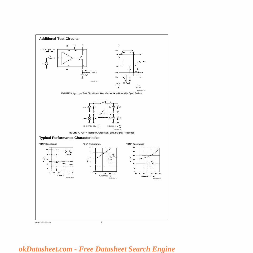
Additional Test Circuits
Typical Performance Characteristics
DS005667-39
DS005667-40
FIGURE 3. tON, tOFF Test Circuit and Waveforms for a Normally Open Switch
DS005667-41
FIGURE 4. “OFF” Isolation, Crosstalk, Small Signal Response
“ON” Resistance
DS005667-23
“ON” Resistance
DS005667-24
“ON” Resistance
DS005667-25
www.national.com 6
okDatasheet.com - Free Datasheet Search Engine
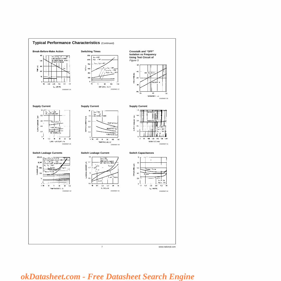
Typical Performance Characteristics (Continued)
Break-Before-Make Action
DS005667-26
Switching Times
DS005667-27
Crosstalk and “OFF”Isolation vs FrequencyUsing Test Circuit ofFigure 5
DS005667-28
Supply Current
DS005667-29
Supply Current
DS005667-30
Supply Current
DS005667-31
Switch Leakage Currents
DS005667-32
Switch Leakage Current
DS005667-33
Switch Capacitances
DS005667-34
www.national.com7
okDatasheet.com - Free Datasheet Search Engine

Typical Performance Characteristics (Continued)
Application Hints
GENERAL INFORMATION
These devices are monolithic quad JFET analog switcheswith “ON” resistances which are essentially independent ofanalog voltage or analog current. The leakage currents aretypically less than 1 nA at 25˚C in both the “OFF”and “ON”switch states and introduce negligible errors in most applica-tions. Each switch is controlled by minimum TTL logic levelsat its input and is designed to turn “OFF” faster than it willturn “ON.” This prevents two analog sources from being tran-siently connected together during switching. The switcheswere designed for applications which requirebreak-before-make action, no analog current loss, mediumspeed switching times and moderate analog currents.
Because these analog switches are JFET rather thanCMOS, they do not require special handling.
LOGIC INPUTS
The logic input (IN), of each switch, is referenced to two for-ward diode drops (1.4V at 25˚C) from the reference supply(VR) which makes it compatible with DTL, RTL, and TTLlogic families. For normal operation, the logic “0” voltage canrange from 0.8V to −4.0V with respect to VR and the logic “1”voltage can range from 2.0V to 6.0V with respect to VR, pro-vided VIN is not greater than (VCC−2.5V). If the input voltageis greater than (VCC−2.5V), the input current will increase. If
the input voltage exceeds 6.0V or −4.0V with respect to VR,a resistor in series with the input should be used to limit theinput current to less than 100µA.
ANALOG VOLTAGE AND CURRENT
Analog Voltage
Each switch has a constant “ON” resistance (RON) for analogvoltages from (VEE+5V) to (VCC−5V). For analog voltagesgreater than (VCC−5V), the switch will remain ON indepen-dent of the logic input voltage. For analog voltages less than(VEE+5V), the ON resistance of the switch will increase. Al-though the switch will not operate normally when the analogvoltage is out of the previously mentioned range, the sourcevoltage can go to either (VEE+36V) or (VCC+6V), whicheveris more positive, and can go as negative as VEE without de-struction. The drain (D) voltage can also go to either(VEE+36V) or (VCC+6V), whichever is more positive, and cango as negative as (VCC−36V) without destruction.
Analog Current
With the source (S) positive with respect to the drain (D), theRON is constant for low analog currents, but will increase athigher currents (>5 mA) when the FET enters the saturationregion. However, if the drain is positive with respect to thesource and a small analog current loss at high analog cur-rents (Note 6) is tolerable, a low RON can be maintained foranalog currents greater than 5 mA at 25˚C.
Slew Rate of AnalogVoltage Above WhichSignal Loading Occurs
DS005667-35
Small Signal Response
DS005667-36
Maximum AccurateAnalog Currentvs Temperature
DS005667-37
Logical “1” Input BiasCurrent
DS005667-38
www.national.com 8
okDatasheet.com - Free Datasheet Search Engine

Application Hints (Continued)
LEAKAGE CURRENTS
The drain and source leakage currents, in both the ON andthe OFF states of each switch, are typically less than 1 nA at25˚C and less than 100 nA at 125˚C. As shown in the typicalcurves, these leakage currents are Dependent on powersupply voltages, analog voltage, analog current and thesource to drain voltage.
DELAY TIMES
The delay time OFF (tOFF) is essentially independent of boththe analog voltage and temperature. The delay time ON(tON) will decrease as either (VCC−VA) decreases or the tem-perature decreases.
POWER SUPPLIES
The voltage between the positive supply (VCC) and either thenegative supply (VEE) or the reference supply (VR) can be asmuch as 36V. To accommodate variations in input logic refer-ence voltages, VR can range from VEE to (VCC−4.5V). Careshould be taken to ensure that the power supply leads for thedevice never become reversed in polarity or that the deviceis never inadvertently installed backwards in a test socket. If
one of these conditions occurs, the supplies would zener aninternal diode to an unlimited current; and result in a de-stroyed device.
SWITCHING TRANSIENTS
When a switch is turned OFF or ON, transients will appear atthe load due to the internal transient voltage at the gate ofthe switch JFET being coupled to the drain and source bythe junction capacitances of the JFET. The magnitude ofthese transients is dependent on the load. A lower value RL
produces a lower transient voltage. A negative transient oc-curs during the delay time ON, while a positive transient oc-curs during the delay time OFF. These transients are rela-tively small when compared to faster switch families.
DISABLE NODE
This node can be used, as shown in Figure 5, to turn all theswitches in the unit off independent of logic inputs. Normally,the node floats freely at an internal diode drop (≈0.7V) aboveVR. When the external transistor in Figure 5 is saturated, thenode is pulled very close to VR and the unit is disabled. Typi-cally, the current from the node will be less than 1 mA. Thisfeature is not available on the LF11201 or LF11202 series.
Typical Applications
DS005667-6
FIGURE 5. Disable Function
Sample and Hold with Reset
DS005667-42
www.national.com9
okDatasheet.com - Free Datasheet Search Engine

Typical Applications (Continued)
Programmable Inverting Non-Inverting Operational Amplifier
DS005667-43
Programmable Gain Operational Amplifier
DS005667-44
www.national.com 10
okDatasheet.com - Free Datasheet Search Engine
Typical Applications (Continued)
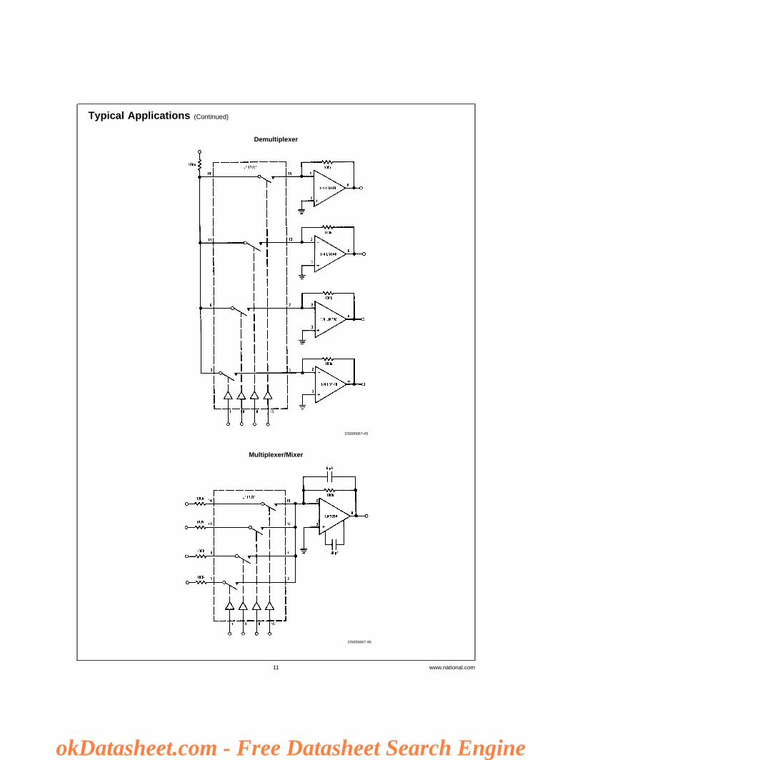
Demultiplexer
DS005667-45
Multiplexer/Mixer
DS005667-46
www.national.com11
okDatasheet.com - Free Datasheet Search Engine

Typical Applications (Continued)
8-Channel Analog Commutator with 6-Channel Select Logic
DS005667-47
Chopper Channel Amplifier
DS005667-48
www.national.com 12
okDatasheet.com - Free Datasheet Search Engine
Typical Applications (Continued)
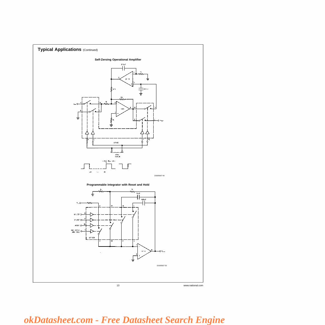
Self-Zeroing Operational Amplifier
DS005667-49
Programmable Integrator with Reset and Hold
DS005667-50
www.national.com13
okDatasheet.com - Free Datasheet Search Engine
Typical Applications (Continued)
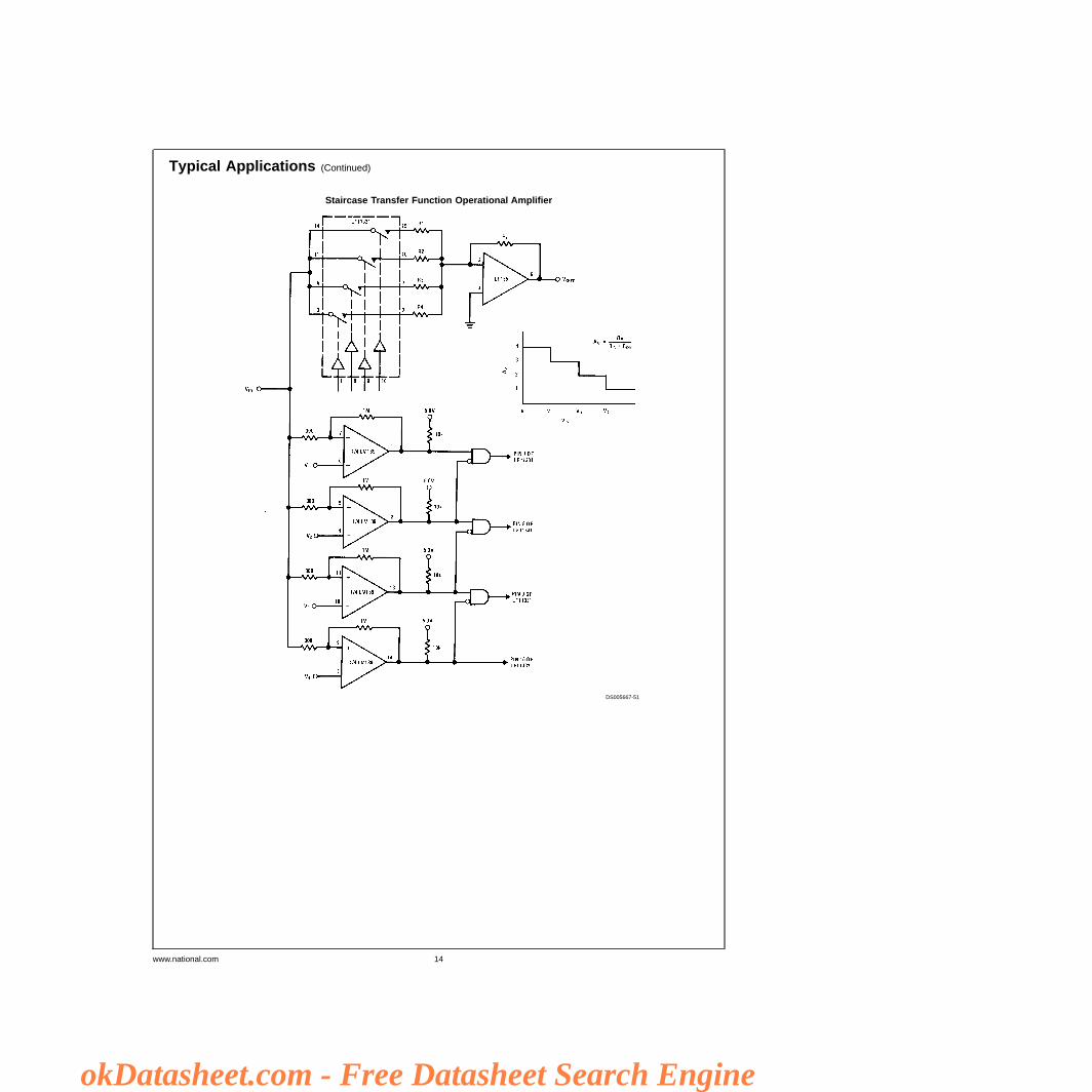
Staircase Transfer Function Operational Amplifier
DS005667-51
www.national.com 14
okDatasheet.com - Free Datasheet Search Engine

Typical Applications (Continued)
DSB Modulator-Demodulator
DS005667-11
www.national.com15
okDatasheet.com - Free Datasheet Search Engine


Physical Dimensions inches (millimeters) unless otherwise noted
Order Number LF11201D, LF11201D/883, LF13201D, LF11202D, LF11202D/883, LF13202D, LF11331D,LF11331D/883, LF13331D, LF11332D, LF11332D/883, LF13332D, LF11333D, LF11333D/883 or LF13333D
NS Package Number D16C
Order Number LF113201M, LF13202M,LF13331M, LF13332M or LF13333M
NS Package Number M16A
www.national.com17
okDatasheet.com - Free Datasheet Search Engine
Physical Dimensions inches (millimeters) unless otherwise noted (Continued)
LIFE SUPPORT POLICY
NATIONAL’S PRODUCTS ARE NOT AUTHORIZED FOR USE AS CRITICAL COMPONENTS IN LIFE SUPPORT DE-VICES OR SYSTEMS WITHOUT THE EXPRESS WRITTEN APPROVAL OF THE PRESIDENT OF NATIONAL SEMI-CONDUCTOR CORPORATION. As used herein:1. Life support devices or systems are devices or sys-
tems which, (a) are intended for surgical implant intothe body, or (b) support or sustain life, and whose fail-ure to perform when properly used in accordancewith instructions for use provided in the labeling, canbe reasonably expected to result in a significant injuryto the user.
2. A critical component is any component of a life supportdevice or system whose failure to perform can be rea-sonably expected to cause the failure of the life supportdevice or system, or to affect its safety or effectiveness.
National SemiconductorCorporationAmericasTel: 1-800-272-9959Fax: 1-800-737-7018Email: [email protected]
www.national.com
National SemiconductorEurope
Fax: +49 (0) 1 80-530 85 86Email: [email protected]
Deutsch Tel: +49 (0) 1 80-530 85 85English Tel: +49 (0) 1 80-532 78 32Français Tel: +49 (0) 1 80-532 93 58Italiano Tel: +49 (0) 1 80-534 16 80
National SemiconductorAsia Pacific CustomerResponse GroupTel: 65-2544466Fax: 65-2504466Email: [email protected]
National SemiconductorJapan Ltd.Tel: 81-3-5639-7560Fax: 81-3-5639-7507
Order Number LF13201N, LF13202N, LF13331N, LF13332N or LF13333NNS Package Number N16A
LF11
331/
LF13
331/
LF11
332/
LF13
332/
LF11
333/
LF13
333/
LF11
201/
LF13
201/
LF11
202/
LF13
202
Qua
dS
PS
TJF
ET
Ana
log
Sw
itche
s
National does not assume any responsibility for use of any circuitry described, no circuit patent licenses are implied and National reserves the right at any time without notice to change said circuitry and specifications.
okDatasheet.com - Free Datasheet Search Engine