frequently asked questions - lime · pdf filefrequently asked questions 2 ... 7.5 can the adc...
TRANSCRIPT
© Copyright Lime Microsystems Proprietary and Confidential
Rev: 1.0r13
Last modified: 15/09/2012
Lime Microsystems Limited
Surrey Tech Centre
Occam Road
The Surrey Research Park
Guildford GU2 7YG
Surrey
United Kingdom
Tel: +44 (0) 1483 685 063
Fax: +44 (0) 1428 656 662
e-mail: [email protected]
Frequently Asked Questions
Frequently Asked Questions
2 | P a g e
© Copyright Lime Microsystems Proprietary and Confidential
Rev: 1.0r13
Last modified: 15/09/2012
Table Of Contents
1. Latest Documentation
1.1 Where can I find the latest datasheet for LMS6002DFN and other related documentation?
2. Graphical User Interface (GUI)
2.1 How can I check SPI connection with Lime GUI?
2.2 Why is it that the GUI does not control LMS6002DFN after a while although setup remains the same?
2.3 Why I cannot lock the PLL, or why Transmitter frequency is not the same as programmed value?
2.4 How can I write register values into a txt file?
3. EVB testing
3.1 How can a 3GGP waveform be transmitted via the LMS6002DFN chip?
3.2 What settings are required for operation with Analog IQ signals?
3.3 Do I need to use the ADF4002 option?
3.4 How should I synchronize measurement equipment with the evaluation/interface board?
3.5 How do I select VCOCAP code for the desired frequency?
3.6 Which clock buffers have to be enabled for the normal operation of LMS6002DFN?
3.7 How should I connect the Lime evaluation board to the HSMC connector?
3.8 Does LMS6002DFN require a specific order for setting up the internal registers on power on? Should there
be a time delay between every register set?
3.9 Where are the spurs coming from around the carrier signal at +/-200 kHz?
3.10 What is the common mode voltage and voltage swing setting to drive Tx Analog (baseband) input ports?
4. Calibration procedures
4.1 What is the LO leakage calibration procedure for transmitter?
4.2 What is the LO leakage calibration procedure for receiver?
4.3 Is LO leakage calibration required when frequency has been changed?
4.4 TX LO leakage is specified as -50 dBc. Can it be maintained over entire TX dynamic range?
4.5 How many clock cycles are required for DC offset calibration?
4.6 Can I use look-up table of LO leakage calibration over multiple frequencies?
4.7 Why TXLPF, RXLPF, and RXVGA2 calibration routines return with DC_LOCK values of 0?
4.8 How to execute calibration routines if there is no read back function in my baseband?
4.9 Can RX calibration be maintained over the entire Rx dynamic range?
5. RF system questions
5.1 What is total power consumption of LMS6002DFN?
5.2 What are the maximum transmitter and receiver gain values?
5.3 What is the receiver and transmitter PLL lock time?
5.4 How to design a new PLL Loop Filter?
5.5 What is the PLL Loop Filter bandwidth?
5.6 What is RF bandwidth of the Tx1 and Tx2 outputs?
5.7 What are the baseband filter bandwidths implemented in LMS6002DFN?
5.8 What is the group delay for 5 MHz and 2.5 MHz filters in LMS6002DFN?
5.9 Does the LNA need to be power down when the RF LOOPBACK is in operation?
5.10 What is the maximum CW signal input level for the receiver?
5.11 What is the IIP3 for the receiver?
5.12 What is the RX Mixer P1dB?
5.13 What is the TX OIP3 (or OIP1) at maximum and minimum gain settings?
5.14 What is RF bandwidth of the receiver inputs?
5.15 What is the TX Noise Figure at maximum gain settings?
5.16 What is transmitter to receiver noise isolation on LMS6002DFN?
Frequently Asked Questions
3 | P a g e
© Copyright Lime Microsystems Proprietary and Confidential
Rev: 1.0r13
Last modified: 15/09/2012
5.17 What is the settling time of TX/RX gain blocks after they are set via SPI control?
5.18 What is recommended gain table for the receiver?
5.19 How can RSSI be used in LMS6002DFN?
5.20 How can the VGA1 code be converted into dB’s?
5.21 Can the envelop detectors within the LMS6002DFN be used for calibration?
5.22 Can the internal LPFs be bypassed?
5.23 What is heat thermal resistance and junction temperature of the LMS6002DFN?
5.24 What is VCO’s frequency range?
5.25 How to set LMS6002DFN for TDD operation?
5.26 How to improve receiver linearity?
5.27 What register have to be changed from default values?
5.28 What is the difference between hardware TXEN and STXEN, similarly for hardware RXEN and SRXEN?
5.29 What is the environmental rating for LMS6002DFN?
5.30 What is the KVCO for the VCO frequencies from 4GHz to 8 GHz?
6. LMS6002DFN digital interface
6.1 Does the LMS6002DFN supports JESD207 interface?
6.2 What are recommended CLK_jitter characteristics for Rx_CLK, Tx_CLK and PLL_CLK?
6.3 Is it possible to use 2.5 V data signal and clock signal with the LMS6002DFN internal DACs and ADCs?
6.4 Is RX_CLK_OUT required for RXD sampling?
6.5 Can the sampling clock/rate for internal DAC and ADC be changed on the evaluation board?
6.6 What is the latency of the data converters within the LMS6002DFN?
6.7 What is the maximum sampling rate for DAC’s and ADC’s?
6.8 What is the recommended signal level of reference clock to drive the internal PLLs?
6.9 What type of coupling should be applied for reference clock to the internal PLLs?
6.10 How to improve ADC’s spectrum?
7. Implementation questions
7.1 What is the recommended footprint for the LMS6002DFN?
7.2 What is the power up, down and the reset sequence for LMS6002DFN?
7.3 What are the recommended power supplies for the LMS6002DFN?
7.4 Is it necessary to connect the Pin #42 ATP (Analog Test Point)?
7.5 Can the ADC be left unconnected if it is not used in my application?
7.6 What is the purpose of the 22 Ohm resistors on pins 60 and 84?
7.7 What is recommended metal mask size and depth for solder paste?
7.8 What is the range of operating moisture condition in %?
7.9 What is package warp after reflow soldering?
7.10 According to “LMS6002Dr2 PCB Layout Recommendations-1.0r06.pdf”, page 2, Figure 5, solder paste for
GND pattern (center pad) is split into grid of 13x7(0.3mmx0.7mm)rectangles. What is the reason? Is
solder volume too much if this GND pattern is not split?
7.11 What is the ramp rate for the LMS6002DFN package?
Frequently Asked Questions
4 | P a g e
© Copyright Lime Microsystems Proprietary and Confidential
Rev: 1.0r13
Last modified: 15/09/2012
Revision History Version 1.0r0
Realeased: Feb 09, 2012
Initial version created
Versions 1.0r1
Released: Mar 28, 2012
Document updated with new QA.
Versions 1.0r2
Released: Apr 13, 2012
Document updated with new QA.
Versions 1.0r3
Released: Apr 13, 2012
Some corrections.
Versions 1.0r4
Released: May 5, 2012
Document updated with new QA.
Versions 1.0r6
Released: May 16, 2012
Updated question 38. Added new question 60,61,62,63.
Versions 1.0r7
Released: Jun 21, 2012
Updated question marking. Added new QA for 4.7, 4.8 and 4.9.
Versions 1.0r8
Released: Aug 22, 2012
Added new QA for 5.25.
Versions 1.0r9
Released: Oct 24, 2012
Added new QA for 5.26 , 5.27, 6.10 and 7.10.
Versions 1.0r10
Released: Oct 25, 2012
Corrected QA 5.27.
Versions 1.0r11
Released: Apr 26, 2012
Added QA 3.10 and 5.28, 5.29. Updated QA 5.23.
Versions 1.0r12
Released: Jun 3, 2012
Added QA 5.30.
Frequently Asked Questions
5 | P a g e
© Copyright Lime Microsystems Proprietary and Confidential
Rev: 1.0r13
Last modified: 15/09/2012
Answers:
1.1 Where can I find the latest datasheet for LMS6002DFN and other related documentation?
In Lime Microsystems Customer Portal. If you don’t have an access please register on
http://www.limemicro.com/register.php and request for portal access.
2.1 How can I check SPI connection with Lime GUI?
On GUI click on Tools>> Register Test. If test results are all OK then SPI communication is working fine.
If test has not passed please check section “4. Installing and Running PC Software Application” in
“LMS6002Dr2-Quick Starter Manual.pdf” document, page 22.
2.2 Why is it that the GUI does not control LMS6002DFN after a while although setup remains the same?
This happens when USB cable is disconnected from the evaluation/interface board while GUI software is
still running. Disconnect USB cable from the evaluation/interface board, close the GUI, connect USB cable
and start the GUI software again.
2.3 Why I cannot lock the PLL, or why is the Transmitter frequency is not the same as the programmed
value?
Please check if your Reference clock is set correctly in the GUI. To check it, click on the tab
Options>>Reference Clock. The Reference Clock frequency window will pop-in. Select or type the
reference clock frequency. Press OK.
2.4 How can I write the register values into a txt file?
LMS6002DFN register setup can be extracted by using the GUI software. Click on File>>Save Registers.
3.1 How can a 3GGP waveform be transmitted via the LMS6002DFN chip?
There are two ways to test 3GPP waveform with Lime Chip: using digital IO, generated with a third party
baseband processor, DSP or FPGA. The other way is by using Analog IQ signals, fed directly to
LMS6002DFN. For example, Analog IQ input signals for Tx can be generated using signal generator with
appropriate IQ modulator option.
3.2 What settings are required for operation with Analog IQ signals?
Using Tx Analog IQ inputs, DACs should be powered down. Using Rx Analog outputs, ADCs should be
power down.
3.3 Do I need to use the ADF4002 option?
Yes. Synchronizing your test and measurement equipment with evaluation board reference clock will cure
the frequency error in your setup. Especially useful in EVM and sensitivity measurement.
3.4 How should I synchronize measurement equipment with the evaluation/interface board?
Connect 10 MHz reference signal to J4 connection on the board. Program onboard ADF4002 with GUI on
the tab called Board.
3.5 How do I select VCOCAP code for the desired frequency?
VCOCAP code have to be tuned when you change frequency. VCO Comparators are implemented on chip
to monitor VCO Tune voltage. This gives a logic 0’s when VCOCAP code value is correct. Calibration
algorithm is described in “LMS6002Dr2-Programming and Calibration Guide-1_1r2.pdf" , chapter “4.6
VCOCAP Code Selection Algorithm”, page 41.
3.6 Which clock buffers have to be enabled for the normal operation of LMS6002DFN?
For full duplex operation only TX DSM SPI and RX DSM SPI have to be enabled. Other clock buffers have
to enabled only for calibration procedures.
3.7 How should I connect the Lime evaluation board to the HSMC connector?
Lime supplies adaptor boards for HSMC connector. For more information please email
Frequently Asked Questions
6 | P a g e
© Copyright Lime Microsystems Proprietary and Confidential
Rev: 1.0r13
Last modified: 15/09/2012
3.8 Does LMS6002DFN require a specific order for setting up the internal registers on power on? Should
there be a time delay between every register set?
There is no particular order required. There is no need to define a time delay between every register set
either.
3.9 Where are the spurs coming from around the carrier signal at +/-200 kHz?
On the evaluation board there is a -5V switching regulator for the differential buffer on the RX analog IQ
outputs, which injects a 240kHz spur into the PLL, but is largely filtered by the 100kHz PLL loop
filter. This spur can be removed by disconnecting the power to the -5V regulator.
3.10 What is the common mode voltage and voltage swing setting to drive Tx Analog (baseband) input
ports? LMS6002D Analog inputs require a 0.6V common mode offset voltage with a 300 mVp-p voltage swing for
optimum performance.
4.1 What is the LO leakage calibration procedure for the transmitter?
Set transmitter for the desire frequency. Set the gain for the required output power. Turn off DAC or set
DAC to generate minimum DC. Make sure that there is no any signal applied at TX RF input during DC
calibration Execute auto DC offset calibration. Minimize LO leakage by manually adjusting I/Q DAC LO
leakage calibration registers. This calibration is described in “LMS6002Dr2-Quick Starter Manual-
EVB_5_r2..pdf” document, on page 66.
4.2 What is the LO leakage calibration procedure for the receiver?
Before calibrating, set the receiver for the desired frequency. Set VGA2 gain to maximum (30 dB). Execute
calibration for RXLPF and RXVGA2 as explained in the data sheet/programming guide, on page 38.
4.3 Is LO leakage calibration required when frequency has been changed?
LO leakage calibration is required if only 3GPP band has been changed. Calibration remains stable over the
entire frequency range within a given 3GPP band.
4.4 TX LO leakage is specified as -50 dBc. Can it be maintained over entire TX dynamic range?
This is specified for maximum transmitter gain. With LO leakage calibration you should be able to achieve -
50 dBc for entire Tx dynamic range and frequency range.
4.5 How many clock cycles are required for DC offset calibration?
DC calibration function takes 64 clock cycles. DC calibration clocks are derived from the PLL reference
clock as follows:
For RXVGA2: cal clock frequency is Fref/16;
For LPF: cal clock frequency is Fref/256;
64 DC cal clock cycles are required per stage (TXLPF=2 stages, RXLPF=2 stages, RXVGA2=5
stages).
4.6 Can I use look-up table for LO leakage calibration over multiple frequencies?
Yes, there are on chip automated DC cancelation/calibration loops. We recommend to execute (trigger)
these at each startup. Other calibration parameters such as TX LO leakage, IQ phase/gain imbalance can be
stored and reloaded every time
4.7 Why TXLPF, RXLPF, and RXVGA2 calibration routines return DC_LOCK value of 0 or 7?
Please note that sometimes DC_LOCK is not reliable indication. The reason for this is the fact that DC
offset compensation DAC step size is smaller around 0V DC which corresponds to DAC code 31dec
meaning "no need to compensate, DC level is good".
Under this condition, comparator responds as:
UP, UP, UP corresponding to DC_LOCK = "111" or
DOWN, DOWN, DOWN corresponding to DC_LOCK = "000" instead of
UP, DOWN, UP, DOWN, ... corresponding to "1010..."
Frequently Asked Questions
7 | P a g e
© Copyright Lime Microsystems Proprietary and Confidential
Rev: 1.0r13
Last modified: 15/09/2012
In this case DC_lock is not reliable indicator of success or failure of DC offset cancellation algorithm. We
suggest to use DC_REG_VAL instead of DC_LOCK as in the pseudo-code below.
execute_DC_CAL();
dc_reg_val = read_DC_REG_VAL();
if( dc_reg_val != 31 ) {
return(OK);
else {
set_DC_REG_VAL(0);
execute_DC_CAL();
dc_reg_val = read_DC_REG_VAL();
if( dc_reg_val != 0 ) {
return(OK);
} else {
return(CHIP_NOT_OK);
}
}
Note that CHIP_NOT_OK condition should not happen as this is being checked in our production test.
4.8 How to execute calibration routines if there is no read back function in my baseband?
You can use calibration sequence as it is shown below:
RX path calibration procedure
# DC Offset calibration of RX I and Q filters
spi_write(0x898C) # Set CLK_EN[3] on
spi_write(0xD308) # Set DC_ADDR[2:0], I filter
spi_write(0xD328) # Set DC_START_CLBR start
spi_write(0xD308) # Set DC_START_CLBR stop
spi_write(0xD309) # Set DC_ADDR[2:0], Q filter
spi_write(0xD329) # Set DC_START_CLBR start
spi_write(0xD309) # Set DC_START_CLBR stop
spi_write(0x8984) # Set CLK_EN[3] off
# DC Offset calibration of RXVGA2
spi_write(0x8994) # Set CLK_EN[4] on
spi_write(0xE600) # Enable comparators
spi_write(0xE308) # Set DC_ADDR[2:0], DC reference module
spi_write(0xE328) # Set DC_START_CLBR start
spi_write(0xE308) # Set DC_START_CLBR stop
spi_write(0xE309) # Set DC_ADDR[2:0], VGA2A Q stage
spi_write(0xE329) # Set DC_START_CLBR start
spi_write(0xE309) # Set DC_START_CLBR stop
spi_write(0xE30A) # Set DC_ADDR[2:0], VGA2A I stage
spi_write(0xE32A) # Set DC_START_CLBR start
spi_write(0xE30A) # Set DC_START_CLBR stop
spi_write(0xE30B) # Set DC_ADDR[2:0], VGA2B Q stage
spi_write(0xE32B) # Set DC_START_CLBR start
spi_write(0xE30B) # Set DC_START_CLBR stop

Frequently Asked Questions
8 | P a g e
© Copyright Lime Microsystems Proprietary and Confidential
Rev: 1.0r13
Last modified: 15/09/2012
spi_write(0xE30C) # Set DC_ADDR[2:0], VGA2B I stage
spi_write(0xE32C) # Set DC_START_CLBR start
spi_write(0xE30C) # Set DC_START_CLBR stop
spi_write(0xE60A) # Disable comparators
spi_write(0x8984) # Set CLK_EN[4] off
TX path calibration procedure
# DC Offset calibration of TX I and Q filters
spi_write(0xD704) # Set ADCs/DACs off
spi_write(0x8942) # Set CLK_EN[1] on
spi_write(0xB308) # Set DC_ADDR[2:0], I filter
spi_write(0xB328) # Set DC_START_CLBR start
spi_write(0xB308) # Set DC_START_CLBR stop
spi_write(0xB309) # Set DC_ADDR[2:0], Q filter
spi_write(0xB329) # Set DC_START_CLBR start
spi_write(0xB309) # Set DC_START_CLBR stop
spi_write(0xD784) # Set ADCs/DACs on
spi_write(0x8981) # Set CLK_EN[1] off
# TX LO leakage calibration
# LO DAC values (77/7F in this case) tuned in production and fixed
spi_write(0xC277) # set I LO cal DAC
spi_write(0xC37F) # set Q LO cal DAC
4.9 Can RX calibration be maintained over the entire Rx dynamic range?
Once RX path is calibrated DC offset will change more with RXVGA1 gain than with RXVGA2 gain.
When you change RXVGA1 gain you have to recalibrate so use RXVGA2 for AGC first before you start
engaging RXVGA1. This behaviour can be improved a lot in digital domain (BB/FPGA) implementing
averaging filter. More information you can find in a “LMS6002D Improving transceiver performance using
digital technics -1.0r1.doc” document.
5.1 What is total power consumption of LMS6002DFN?
In full duplex mode at maximum gain the power dissipation is around 1.5W.
5.2 What are the maximum transmitter and receiver gain values?
Transmitter gain consists of: TX LPF Gain 6dB, TX VGA1 gain -4dB, TX VGA2 Gain 25dB, total gain is
+27dB.
Receiver gain consists of: RX LNA Gain 12dB, RX VGA1 gain 30dB, LPF Gain 6dB and RX VGA2 Gain
30dB, total is +78dB
5.3 What is the receiver and transmitter PLL lock time?
Maximum PLL lock time is 20us.
5.4 How to design a new PLL Loop Filter?
Loop filter has already been designed and optimized for LMS6002DFN. Please refer to reference/EVB
board schematic “REF6002-15 Schematics.pdf”, page 5 or “EVB6002-6_schematics_v1.pdf”, page 6.
5.5 What is The PLL Loop Filter bandwidth?
Loop filter is designed for 100 kHz bandwidth.

Frequently Asked Questions
9 | P a g e
© Copyright Lime Microsystems Proprietary and Confidential
Rev: 1.0r13
Last modified: 15/09/2012
5.6 What is RF bandwidth of the Tx1 and Tx2 outputs?
Both transmitter outputs RF bandwidth is same from 0.3 GHz to 3.8 GHz. On evaluation board Tx1 is
matched to 3GPP Band1 and Tx2 has an Broadband matching network.
5.7 What are the baseband filter bandwidths implemented in LMS6002DFN?
The baseband filter bandwidth can be selected from 0.75 – 14 MHz IF, giving an RF bandwidth from 1.5
MHz – 28 MHz.
5.8 What is the group delay for 5 MHz and 2.5 MHz filters in LMS6002DFN?
The group delay of 5 MHz filter is around 300 ns. For 2.5 MHz group delay is 600ns.
5.9 Does the LNA need to be power down when the RF LOOPBACK is in operation?
For testing purposes the LNA does not need to be powered down. If this is to be done in the field, to avoid
any interference, LNA must be powered down. To do this you will have to enable Direct signals in RxFE
tab Direct Signals [0x7003] and deselect LNA Modules [0x7D01].
5.10 What is the maximum CW signal input level for the receiver?
The maximum CW signal level for the receiver LNA2, with maximum gain, at frequency of 1.95 GHz is -60
dBm. Input signal varies with the frequency.
5.11 What is the IIP3 for the receiver?
The RX IIP3 is frequency dependent. The IIP3 for the receive LNA2 is -1dB, at 1.95 GHz.
5.12 What is the RX Mixer P1dB?
The Rx Mixer Input IP3 = 22.5 dBm hence the Mixer input P1dB would be 11 dBm.
5.13 What is the TX OIP3 (or OIP1) at maximum and minimum gain settings?
TX OIP3 is frequency dependent. OP1dB is about +15 dBm at maximum gain and OIP3 is typically 10 dB
higher. Reducing VGA2 gain by 25 dB, the OP1dB and OIP3 will fall by 25 dB.
5.14 What is RF bandwidth of the receiver inputs?
The RX LNA1 RF bandwidth is from 0.3 – 2.8 GHz, Rx LNA2 is 1.5 – 3.8 GHz, Rx LNA3 is 0.3 – 3.0
GHz.
5.15 What is the TX Noise Figure at maximum gain settings?
TX Noise Figure is largely defined by TXLPF and TXDAC. Low Pass Filter noise figure is about 35 dB
relative to 50 Ohm.
5.16 What is transmitter to receiver noise isolation on LMS6002DFN?
Measured transmitter noise on receiver 3GPP Bands: Band 1 – -135dBm/Hz with TX output -2.2 dBm/3.84
MHz; Band 5 – -131.2 dBm/Hz with TX output 2.85 dBm/3.84 MHz;
5.17 What is the settling time of TX/RX gain blocks after they are set via SPI control?
Settling time of each gain block in LMS6002DFN is less than 100ns.
5.18 What is recommended gain table for the receiver?
LMS6002DFN does not have RSSI blocks. Below is a gain table developed for WCDMA and can be used
for other modulation schemes:
Min. Signal
(dBm)
Max. Signal
(dBm)
SNR(dB)
Min.
SNR(dB)
Max.
Antenna
Switch LNA Gain
RxVGA1
gain
RxVGA2
gain
-117 ** -85 -17.4 14.6 - Max. Max. Max.
-84 * -53 15.6 46.6 - Max. Max. Variable
-52 -28 47.6 71 - Max. Variable Min.
-27 -22 69.46 74.46 - Mid (Max - 6 dB) Min. Min.
-21 -13 67.98 75.98 - Bypassed Min. Min.
-12 4 60.5 76.48 Switched Bypassed Min. Min.

Frequently Asked Questions
10 | P a g e
© Copyright Lime Microsystems Proprietary and Confidential
Rev: 1.0r13
Last modified: 15/09/2012
Table 1. Receiver gain table versus modulated input signal level 3GPP Band 1 (1950MHz) .
Min. Signal
(dBm)
Max. Signal
(dBm)
SNR(dB)
Min.
SNR(dB)
Max.
Antenna
Switch LNA Gain
RxVGA1
gain
RxVGA2
gain
-119 ** -85 -19.49 14.5 - Max. Max. Max.
-84 * -53 15.5 46.5 - Max. Max. Variable
-52 -39 47.5 54.75 - Max. Variable Min.
-38 -32 51.25 57.25 - Mid (Max - 6 dB) Min. Min.
-31 -13 51.5 69.5 - Bypassed Min. Min.
-12 4 - - Switched Bypassed Min. Min.
Table 2. Receiver gain table versus modulated input signal level for Band 5 (840 MHz).
Notes: * - Sensitivity measured with WCDMA 12.2 RMC Signal. Processing gain 25 dB.
** - Minimum Eb/No = 5.7 dB.
5.19 How can RSSI be used in LMS6002DFN?
There is no RSSI block in LMS6002DFN chip. RSSI can be calculated digitally using BB/FPGA as
RSSI=SQRT(I*I+Q*Q).
5.20 How can the VGA1 code be converted into dB’s?
Please use this formula: G [dB] = 20*log10(127/(127-Code)), where Code is gain control word, 0 <= Code
<= 120.
5.21 Can the envelop detectors within the LMS6002DFN be used for calibration?
On chip peak detectors are working however providing 30 – 40dB dynamic range only which may not be
enough for most calibration requirements. In any case, the level of un-calibrated TX LO leakage is already
low enough so cannot be detected by the internal detectors. We recommend to put peak detector after
external PA and use it for calibration.
5.22 Can the internal LPFs be bypassed?
Internal TX/RX LPFs can be bypassed.
5.23 What is heat thermal resistance and junction temperature of the LMS6002DFN?
The LMS6002DFN package has a 22°C/W thermal resistance (θja) to free air. If this is soldered to the
board, then the thermal resistance of the complete unit from junction, through the case, through the board
and to free air (not forced) becomes a calculated θja = 19.7°C/W, developed as:
θja (junction to air, soldered to the board) = θca (thermal resistance from the case interface on the board to
air) + θjc (thermal resistance junction to case) = 14.0 + 5.7 = 19.7°C/W.
These numbers are extracted using Lime recommended layout. Using these calculations show that with a
typical application having 1.5W dissipation, the chip temperature will be 1.5*19.7 ~29.8°C above ambient.
Frequently Asked Questions
11 | P a g e
© Copyright Lime Microsystems Proprietary and Confidential
Rev: 1.0r13
Last modified: 15/09/2012
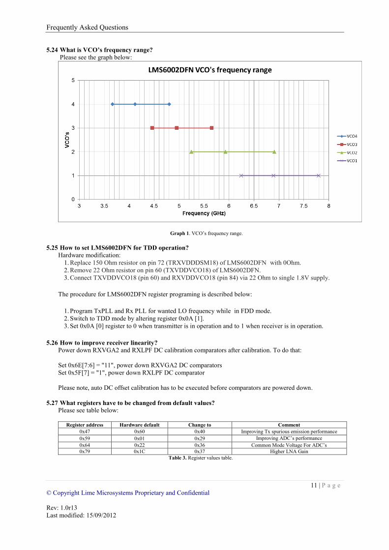
5.24 What is VCO’s frequency range?
Please see the graph below:
Graph 1. VCO’s frequency range.
5.25 How to set LMS6002DFN for TDD operation?
Hardware modification:
1. Replace 150 Ohm resistor on pin 72 (TRXVDDDSM18) of LMS6002DFN with 0Ohm.
2. Remove 22 Ohm resistor on pin 60 (TXVDDVCO18) of LMS6002DFN.
3. Connect TXVDDVCO18 (pin 60) and RXVDDVCO18 (pin 84) via 22 Ohm to single 1.8V supply.
The procedure for LMS6002DFN register programing is described below:
1. Program TxPLL and Rx PLL for wanted LO frequency while in FDD mode.
2. Switch to TDD mode by altering register 0x0A [1].
3. Set 0x0A [0] register to 0 when transmitter is in operation and to 1 when receiver is in operation.
5.26 How to improve receiver linearity? Power down RXVGA2 and RXLPF DC calibration comparators after calibration. To do that:
Set 0x6E[7:6] = "11", power down RXVGA2 DC comparators
Set 0x5F[7] = "1", power down RXLPF DC comparator
Please note, auto DC offset calibration has to be executed before comparators are powered down.
5.27 What registers have to be changed from default values?
Please see table below:
Register address Hardware default Change to Comment
0x47 0x60 0x40 Improving Tx spurious emission performance
0x59 0x01 0x29 Improving ADC’s performance
0x64 0x22 0x36 Common Mode Voltage For ADC’s
0x79 0x1C 0x37 Higher LNA Gain
Table 3. Register values table.

Frequently Asked Questions
12 | P a g e
© Copyright Lime Microsystems Proprietary and Confidential
Rev: 1.0r13
Last modified: 15/09/2012
5.28 What is the difference between hardware TXEN and STXEN, similarly for hardware RXEN and
SRXEN? SRXEN/STXEN registers equivalent to TXEN/RXEN pins. The internal control signals are constructed
using logical AND in the following way:
iTXEN = TXEN and STXEN
iRXEN = RXEN and SRXEN
5.29 What is the environmental rating for LMS6002DFN?
The LMS6002DFN chip is specified for industrial environment, based on JESD47G-01 standard.
5.30 What is the KVCO for the VCO frequencies from 4GHz to 8 GHz?
Please see the graph below.
Graph 2. KVCO value for each VCO.
6.1 Does the LMS6002DFN supports JESD207 interface?
Yes. Lime has developed VHDL code to support JESD207 interface. Please request through
6.2 What are the recommended CLK_jitter characteristics for Rx_CLK, Tx_CLK and PLL_CLK?
TXCLK, RXCLK require the usual jitter specs for the 12 bit DACs/ADCs. Less jitter (better phase noise) of
PLLCLK results in improved phase noise in PLL and overall system EVM.
6.3 Is it possible to use 2.5 V data and clock signals with the LMS6002DFN internal DACs and ADCs?
Yes. For more information please go to datasheet section “Implementation Low Voltage Digital IQ
Interface”, page 9.
6.4 Is RX_CLK_OUT required for RXD sampling?
No, but can be used. Please follow the reference schematic of RX_CLK layout in document “REF6002-15
Schematics.pdf”, page 2.
0
20
40
60
80
100
120
140
160
180
3.5 4 4.5 5 5.5 6 6.5 7 7.5 8 8.5
KV
CO
MH
z/V
VCO Frequency, GHz
KVCO over the VCOCAP range Vtune is 1.5V
VCO1
VCO2
VCO3
VCO4

Frequently Asked Questions
13 | P a g e
© Copyright Lime Microsystems Proprietary and Confidential
Rev: 1.0r13
Last modified: 15/09/2012
6.5 Can the sampling clock/rate for the internal DAC and ADC be changed on the evaluation board?
The sampling clock can be changed depending on the clock source. That will require some 0 Ohm link
soldering/disordering. All clock distribution options are described in Quick Start Manual.pdf document
section “3.4 TCXO Frequency and Data Clocks Distribution”, page 17.
6.6 What is the latency of the data converters within the LMS6002DFN ?
DAC and ADC latency is around 10 TXCLK/RXCLK cycles and is not changing with the setup.
6.7 What is the maximum sampling rate for DAC’s and ADC’s?
Maximum sampling rate for DAC’s and ADC’s is 40MHz. Sampling rate is defined by the rate at which the
pins of TXCLK (pin 19) and RXCLK (pin 17) signal lines can be clocked. These are twice the data
converters sampling rate. For more information please refer to data-sheet section “Digital IQ Data
Interface”, page 6.
6.8 What is the recommended signal level of reference clock to drive the internal PLLs? Recommended level for PLL reference clock is 3.3Vpp, CMOS type signal.
6.9 What type of coupling should be applied for reference clock to the internal PLLs?
By default, PLL clock input buffer is set to AC coupling mode. The same setting can also be used in DC
coupling mode
6.10 How to improve ADC’s spectrum?
RXVGA2 CM voltage code has to be set to 13 which corresponds to 0.82 V (register 0x64[5:2] = '1101').
Also set ADC reference gain adjustment to 1.75 V (register 0x59 [6:5] = '01').
7.1 What is the recommended footprint for the LMS6002DFN?
Lime offer two types of footprints for LMS6002DFN, via in pad and via off pad. The latter version is a cost
reduced option by avoiding the in pad vias. Both footprints are tested and verified as reliable to be used in
production. Please refer to “LMS6002Dr2 PCB Layout Recommendations-1.0r0.pdf” document.
7.2 What is the power up, down and reset sequence for LMS6002DFN?
There is no particular power up sequence required. As usual, it is recommended ESD (3.3V) supplies to
come up first and go off last. However, there is no issue even if this timing is violated for short period. See
pin description in the data sheet to identify ESD pins, table 12 page 12.
A low pulse (10ns min) on RESET pin is recommended.
7.3 What are the recommended power supplies for the LMS6002DFN?
Switcher can be used for 3.3V. LDO is recommended for 1.8V to ensure a clean VCO supply.
7.4 Is it necessary to connect the Pin #42 ATP (Analog Test Point)?
Analog test point is made for production test. It should be left open. Please refer to reference schematic
“REF6002-15 Schematics.pdf”, page 2.
7.5 Can the ADC be left unconnected if it is not used in my application? Yes.
7.6 What is the purpose of the 22 Ohm resistors on pins 60 and 84?
The purpose of 22 Ohm resistor on pins 60 and 84 is to improve IQ phase imbalance. This also reduces
VCO current from 40 mA down to 20 mA.
7.7 What is recommended metal mask size and depth for solder paste?
The design is constrained by the 14x14 pads on the inner row. This will not print well on a 5 mil foil so we
reduced the foil to 4 mil.
7.8 What is the range of operating moisture condition in %?
After 168 hours at < 30C, 60% relative humidity.

Frequently Asked Questions
14 | P a g e
© Copyright Lime Microsystems Proprietary and Confidential
Rev: 1.0r13
Last modified: 15/09/2012
7.9 What is package warp after reflow soldering?
Package warp should not exceed 0.05mm.
7.10 According to “LMS6002Dr2 PCB Layout Recommendations-1.0r06.pdf”, page 2, Figure 5, solder
paste for GND pattern (center pad) is split into grid of 13x7(0.3mmx0.7mm)rectangles. What is
the reason? Is solder volume too much if this GND pattern is not split?
The grid serves two purposes - to reduce volume so that it does not float too high and yet has good coverage
to dissipate heat, and to avoid vias as much as possible. 40% is a good rule of thumb commonly used.
Although it is typically done with a simple window pane. 25% is a typical minimum to ensure coverage and
yet not sit too low.
Using a solid block would be bad as it would cause open circuits on the outside pads and may cause the
device to spin during reflow. Lots of little pads will typically all reflow at the same time whereas one large
pad will reflow as the heat hits it and not all at the same time. This can cause the device to rotate during
reflow.
Our assembly house has special design software which automatically calculates the ratio of stencil paste
surface area in contact with the pad to the side wall surface area of the stencil, referred to as the "print area
ratio", all designs are passed through this checking software. As a result a 3mil stencil was chosen to make
sure the pads could print OK.
7.11 What is the ramp rate for the LMS6002DFN package?
The ramp rate is shown in the graph below.
Graph 3. The ramp rate for LMS6002DFN