fs8170 2.5 ghz low power phase-locked loop ic · fs8170 2.5 ghz low power phase-locked loop ic ......
TRANSCRIPT
FS8170 2.5 GHz Low Power Phase-locked Loop IC
Princeton Technology Corp. reserves the right to change the product described in this datasheet. All information con-tained in this datasheet is subject to change without prior notice. Princeton Technology Corp. assumes no responsibilityfor the use of any circuits shown in this datasheet.
DescriptionThe FS8170 IC is a serial data input, fully programmable phase-locked loop with a 2.5GHz prescaler for use in the local oscillator subsystem of radio transceivers. Multi-modu-lus division ratios of 32/33 and 64/65 are selectable thru serial programming to enablepulse swallowing operation. When combined with an external VCO, the FS8170 becomesthe core of a very low power frequency synthesizer well-suited for mobile communicationapplications, such as 2.4 GHz ISM-band wireless data links and cellular GSM and PCS.The FS8170 is also pin compatible with Fujitsu’s MB15E07SL IC.
FeaturesMaximum input frequency: 2.5 GHz
Supply voltage range from 2.4 V to 3.6 V
Low current consumption in locked state: 3.5 mA typ. (VCC = VP = 2.7 V, TA = +25 °C)4.0 mA typ. (VCC = VP = 3.0 V, TA= +25 °C)10 µA max. in asynchronous power-down mode
Digitally-filtered lock detect output
18-bit programmable input frequency divider using ÷ 32/33/64/65 multi-modulus prescaler with divide ratio range from 992 to 65631 for ÷ 32/33 mode and from 4032 to 131135 for ÷ 64/65 mode14-bit programmable reference frequency divider with divide ratio range from 3 to 16383
Programmable charge pump current: 1.5 mA or 6 mA
Pin compatible with Fujitsu MB15E07, MB15E07L, MB15E07SL
16 pin, plastic TSSOP (0.65 mm pitch)
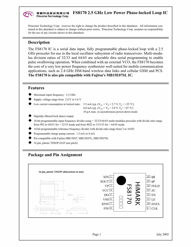
Package and Pin Assignment
16 pin, plastic TSSOP (dimensions in mm)
XINXOUT
VPVCC
DOVSS
XFINFIN
φRφPFOLDZCENLEDATACLK
1
2
3
4
5
6
7
8
16
15
14
13
12
11
10
9
HiMARK
FS8170
Page 1 July 2005
FS8170
Pin Descriptions
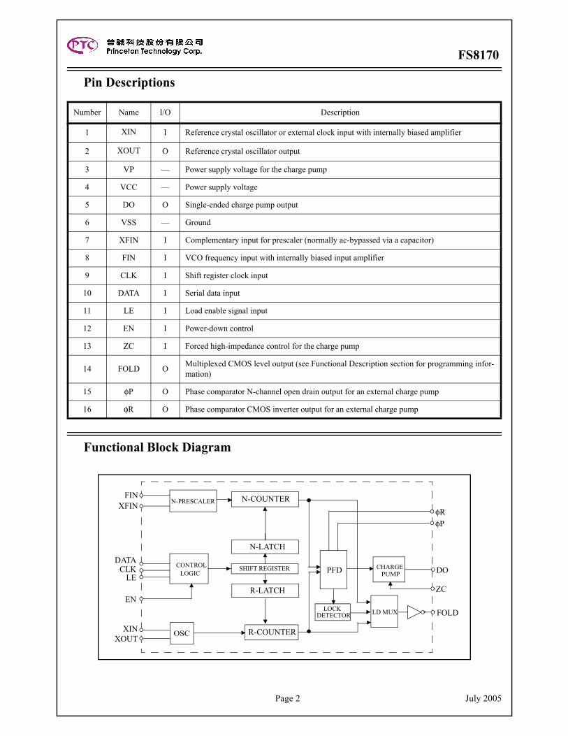
Functional Block Diagram
Number Name I/O Description
1 XIN I Reference crystal oscillator or external clock input with internally biased amplifier
2 XOUT O Reference crystal oscillator output
3 VP — Power supply voltage for the charge pump
4 VCC — Power supply voltage
5 DO O Single-ended charge pump output
6 VSS — Ground
7 XFIN I Complementary input for prescaler (normally ac-bypassed via a capacitor)
8 FIN I VCO frequency input with internally biased input amplifier
9 CLK I Shift register clock input
10 DATA I Serial data input
11 LE I Load enable signal input
12 EN I Power-down control
13 ZC I Forced high-impedance control for the charge pump
14 FOLD O Multiplexed CMOS level output (see Functional Description section for programming infor-mation)
15 φP O Phase comparator N-channel open drain output for an external charge pump
16 φR O Phase comparator CMOS inverter output for an external charge pump
PFD
LD MUX
FIN
DATACLK
LECONTROL
LOGICSHIFT REGISTER
FOLD
DO
LOCKDETECTOR
EN
N-LATCH
N-COUNTER
R-COUNTER
CHARGEPUMP
OSC
N-PRESCALER
XOUTXIN
R-LATCH
XFINφRφP
ZC
Page 2 July 2005
FS8170
Absolute Maximum RatingsVSS = 0 V
Recommended Operating ConditionsVSS = 0 V
Parameter Symbol Rating Unit
Supply voltage rangeVCC VSS – 0.3 to VSS + 4.0 V
VP VCC to 6.0 V
Input voltage range VFIN VSS – 0.5 to VDD + 0.5 V
Output voltage rangeVO VSS to VCC V
VDO VSS to VP V
Storage temperature range TSTG –55 to 125 °C
Soldering temperature range TSLD 260 °C
Soldering time range tSLD 4 s
ESD rating (human body mode) 3500 eV
Parameter SymbolValue
Unitmin. typ. max.
Supply voltage rangeVCC 2.4 3.0 3.6 V
VP Vcc – 5.5 V
Operating temperature TA –40 25 80 °C
Page 3 July 2005
FS8170
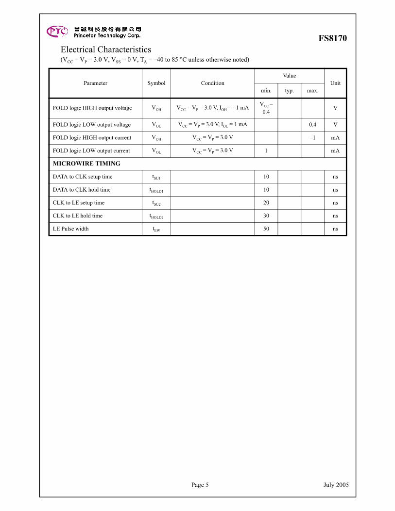
Electrical Characteristics(VCC = VP = 3.0 V, VSS = 0 V, TA = –40 to 85 °C unless otherwise noted)
Parameter Symbol ConditionValue
Unitmin. typ. max.
GENERAL
Power supply current consumption ICC,total fin = 2.5 GHz 4 mA
Standby current consumption ICC,standby ZC = “H” or open 10 µA
FIN operating frequency fFIN VFIN = 0.3 Vpk-pk sinusoid 50 2500 MHz
XIN operating frequency fXIN 3 40 MHz
Input sensitivity PFIN 50 Ω measurement system -15 +2 dBm
XIN input voltage swing VXIN 0.5 VCC Vpk-pk
CHARGE PUMP
RF charge pump output current
IDOsource VDO = VP/2, CS bit = “H” -6 mA
IDOsink VDO = VP/2, CS bit = “H” 6 mA
IDOsource VDO = VP/2, CS bit = “L” -1.5 mA
IDOsink VDO = VP/2, CS bit = “L” 1.5 mA
DIGITAL INTERFACE (DATA, CLK, LE, PS, ZC)
High-level input voltage VIH 0.8×VCC V
Low-level input voltage VIL 0.2×VCC V
High-level input current IIH VIH = VCC = 3.6V –1 1 µA
Low-level input current IIL VIL = 0 V, VCC = 3.6V –1 1 µA
XIN logic HIGH input current IIH,XIN VIH = VDD 100 µA
XIN logic LOW input current IIL,XIN VIL = 0 V –100 µA
φP logic LOW output voltage VOL Open drain output 0.4 V
φP logic LOW output current IOL Open drain output 1 mA
φR logic HIGH output voltage VOH VCC = VP = 3.0 V, IOH = –1 mA VCC –0.4
V
φR logic LOW output voltage VOL VCC = VP = 3.0 V, IOL = 1 mA 0.4 V
φR logic HIGH output current IOH VCC = VP = 3.0 V –1 mA
φR logic LOW output current IOL VCC = VP = 3.0 V 1 mA
Page 4 July 2005
FS8170
FOLD logic HIGH output voltage VOH VCC = VP = 3.0 V, IOH = –1 mA VCC –0.4
V
FOLD logic LOW output voltage VOL VCC = VP = 3.0 V, IOL = 1 mA 0.4 V
FOLD logic HIGH output current VOH VCC = VP = 3.0 V –1 mA
FOLD logic LOW output current VOL VCC = VP = 3.0 V 1 mA
MICROWIRE TIMING
DATA to CLK setup time tSU1 10 ns
DATA to CLK hold time tHOLD1 10 ns
CLK to LE setup time tSU2 20 ns
CLK to LE hold time tHOLD2 30 ns
LE Pulse width tEW 50 ns
Electrical Characteristics(VCC = VP = 3.0 V, VSS = 0 V, TA = –40 to 85 °C unless otherwise noted)
Parameter Symbol ConditionValue
Unitmin. typ. max.
Page 5 July 2005
FS8170
Functional Description
Programmable Input Frequency DividerThe VCO output to the FIN pin is divided by the programmable divider and then inter-nally output to the phase/frequency detector (PFD) as fV. The programmable input fre-quency divider consists of a multi-modulus (selectable ÷ 32/33 or ÷ 64/65 (M/M+1)) prescaler and a 18-bit N-counter, which is further comprised of a 7-bit swallow A-counter, and a 11-bit main B-counter. The total divide ratio, N, is related to values for M, A, and B through the relation
with The minimum programmable divisor for continuous counting is given by , and is for the ÷ 32/33 prescaler mode, and is
for the ÷ 64/65 mode. Hence, the valid total divide ratio range for the input divider is for the ÷ 32/33 mode and for the ÷ 64/65 mode.
Programmable Reference Frequency DividerThe crystal oscillator output is divided by the programmable reference divider and then internally output to the PFD as fR. The programmable reference frequency divider con-sists of a 14-bit reference R-counter. Becasue of its specific design, the minimum accept-able divisor for R is 3, and hence the total divide ratio, R, ranges from 3 to 16383.
Shift Register ConfigurationThe divide ratios for the input and reference dividers are input using a 19-bit serial inter-face consisting of separate clock (CLK), data (DATA), and load enable (LE) lines. The format of the serial data is shown in Table 1. The data on the DATA line is written to the shift register on the rising edge of the CLK signal and is input with MSB first, and the last bit is used as the latch select control bit. The data on the DATA line should be changed on the falling edge of CLK, and LE should be held LOW while data is being written to the shift register. Data is transferred from the shift register to one of the frequency divider latches when LE is set HIGH. When the latch select control bit is set LOW, data is loaded to the 18-bit N-counter latch, and when the latch select control bit is set HIGH, the 4 MSBs are recognized as CS, LDS, FC, SW, respectively, and the next 14 data bits are loaded to the 14-bit R-counter latch. The definition of the 4 MSBs will be described in Table 5 and 6. Note that LDS should be set LOW for normal operation.
Also, serial input data timing waveforms are shown in Fig. 1.
N M 1+( ) A M B A–( )×+× M B A,+×= =
B A.≥M M 1–( )× 32 32 1–( )× 992=64 64 1–( )× 4032=
N 992 to 65631= N 4032 to 131135=
Page 6 July 2005
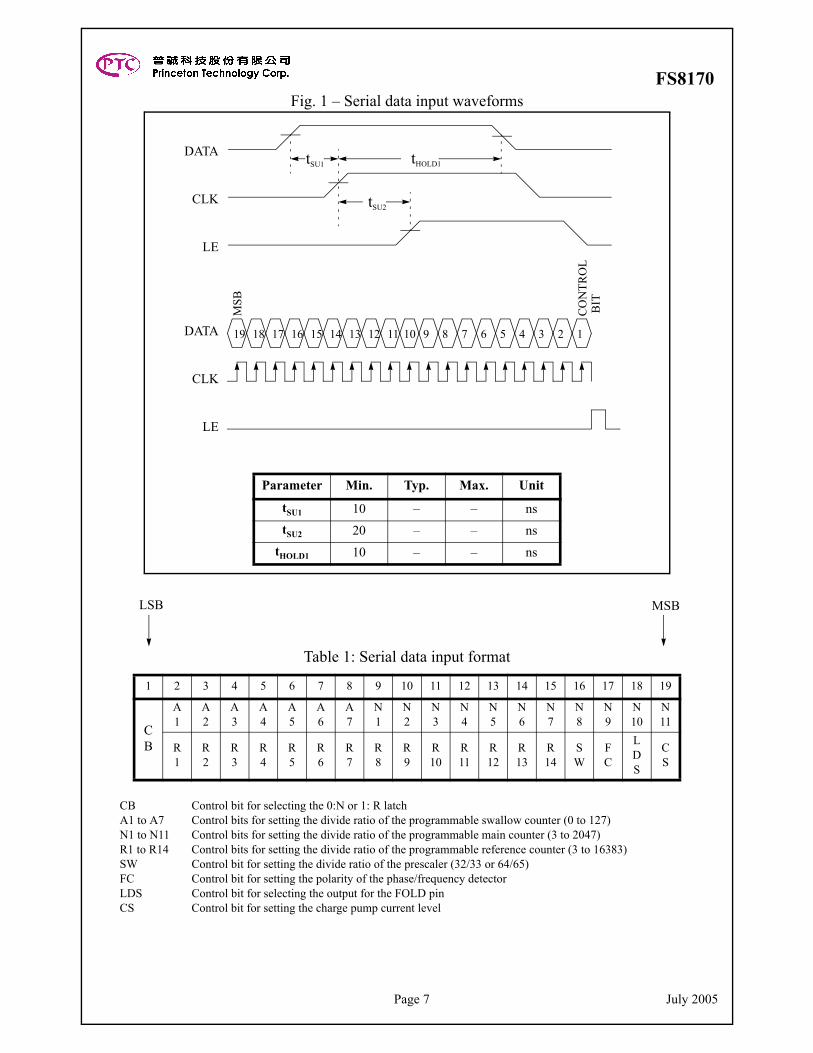
FS8170Fig. 1 – Serial data input waveforms
tSU1
tSU2
tHOLD1DATA
CLK
LE
DATA
CLK
LE
MSB
18 17 16 15 14 13 12 11 10 9 8 7 6 5 4 319 2 1
CO
NTR
OL
Parameter Min. Typ. Max. Unit
tSU1 10 – – nstSU2 20 – – ns
tHOLD1 10 – – ns
BIT
CB Control bit for selecting the 0:N or 1: R latchA1 to A7 Control bits for setting the divide ratio of the programmable swallow counter (0 to 127)N1 to N11 Control bits for setting the divide ratio of the programmable main counter (3 to 2047)R1 to R14 Control bits for setting the divide ratio of the programmable reference counter (3 to 16383)SW Control bit for setting the divide ratio of the prescaler (32/33 or 64/65)FC Control bit for setting the polarity of the phase/frequency detectorLDS Control bit for selecting the output for the FOLD pinCS Control bit for setting the charge pump current level
Table 1: Serial data input format
1 2 3 4 5 6 7 8 9 10 11 12 13 14 15 16 17 18 19
CB
A1
A2
A3
A4
A5
A6
A7
N1
N2
N3
N4
N5
N6
N7
N8
N9
N10
N11
R1
R2
R3
R4
R5
R6
R7
R8
R9
R10
R11
R12
R13
R14
SW
FC
LDS
CS
MSBLSB
Page 7 July 2005
FS8170
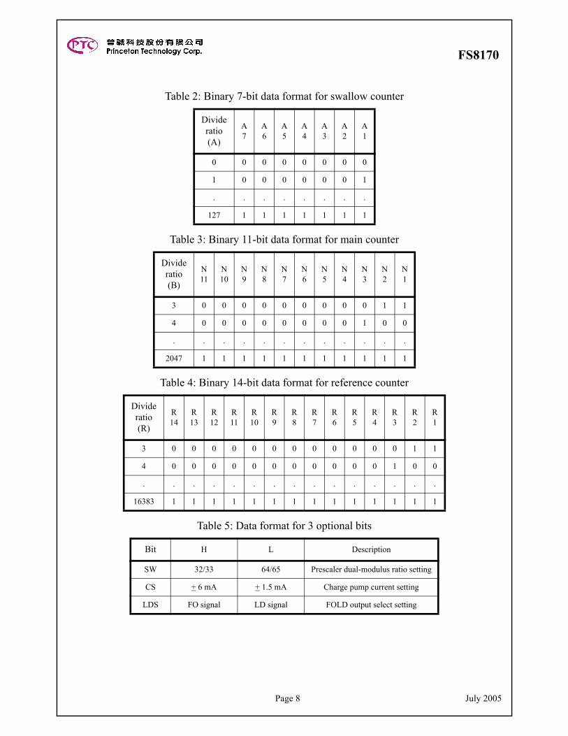
Table 2: Binary 7-bit data format for swallow counter
Divideratio(A)
A7
A6
A5
A4
A3
A2
A1
0 0 0 0 0 0 0 0
1 0 0 0 0 0 0 1
. . . . . . . .
127 1 1 1 1 1 1 1
Table 3: Binary 11-bit data format for main counter
Divideratio(B)
N11
N10
N9
N8
N7
N6
N5
N4
N3
N2
N1
3 0 0 0 0 0 0 0 0 0 1 1
4 0 0 0 0 0 0 0 0 1 0 0
. . . . . . . . . . . .
2047 1 1 1 1 1 1 1 1 1 1 1
Table 4: Binary 14-bit data format for reference counter
Divideratio(R)
R14
R13
R12
R11
R10
R9
R8
R7
R6
R5
R4
R3
R2
R1
3 0 0 0 0 0 0 0 0 0 0 0 0 1 1
4 0 0 0 0 0 0 0 0 0 0 0 1 0 0
. . . . . . . . . . . . . . .
16383 1 1 1 1 1 1 1 1 1 1 1 1 1 1
Table 5: Data format for 3 optional bits
Bit H L Description
SW 32/33 64/65 Prescaler dual-modulus ratio setting
CS + 6 mA + 1.5 mA Charge pump current setting
LDS FO signal LD signal FOLD output select setting
Page 8 July 2005

FS8170
Phase/Frequency Detector (PFD)The PFD compares an internal input frequency divider output signal, fV, with an internalreference frequency divider output signal, fR, and generates an error signal, DO, which isproportional to the phase error between fV and fR. The DO output is intended for use witha passive filter as shown in Fig. 2 (a). The polarity of DO is selectable by setting the bit FCto high or low. The setting should depend on the frequency-voltage characteristic of exter-nal VCO as depicted in Fig. 2 (b).
The input/output waveforms for the PFD are shown in Fig. 3.
Fig. 2 – Low-pass filter and external VCO frequency-voltage characteristic
Table 6: Data format for FC bit (LDS = HIGH)
FC = HIGH FC = LOW
DO φR φP FOLD DO φR φP FOLD
fR > fV H L LFOLD = fR
L H Za
FOLD = fV
fR < fV L H Z H L L
fR = fV Z L Z Z L Z
a. Z denotes high impedance state
DO VCO
(a) Passive low-pass filter
(1)
(2)
fVCO
VDO
(b) VCO frequency-voltage characteristic
Note: If VCO has a positive tuning curve similiar to trace (1), set FC = “H,” otherwise if the VCO has a negative tuning curve similar to trace (2), set FC = “L.”
Page 9 July 2005

FS8170Fig. 3 – Phase comparator output waveforms
Charge Pump (CP)The phase error signal, DO, generated from the PFD will pump charge into an externalloop filter, which then converts the charge to produce the VCO’s tuning voltage. With aconstant pumping rate, the shift of the VCO’s tuning voltage will be directly proportionalto the phase error signal DO. Two pumping rates, 1.5 mA and 6 mA, are provided by thechip and are selectable through the bit CS as defined previously in Table 5. Also, thecharge pump characteristics corresponding to both modes are shown in the Typical Char-acteristics section. The internal charge pump may be turned off by the pin ZC. When ZCis set low, the internal charge pump will stay in its high-impedance state and will not pumpany charge into the external LPF. In this case, the user is allowed to utilize one’s owncharge pump by two control pins φP and φR which are defined in Table 6. φP and φR arethe error signals directly proportional to the positive/negative phase error when FC = “H.”When FC = “L,” the relation becomes negative/positive.
Table 7: Setting for the pin ZC
ZC Do Output
H Normal output
L High impedance
fR
fV
DO
LD
[FC=”H”]
DO[FC=”L”]
1. Pulses of finite width on DO output are generated during locked state to prevent dead zone.2. A “locked” condition (LD is HIGH) is indicated when the phase error is less than t1 or t2 at least for
3 consecutive comparison cycles, otherwise an “unlocked” condition (LD is LOW) is indicated.3. The values of t1 and t2 depend on the XIN input frequency: t1 > 2/fosc (e.g. t1 > 250 ns, if fXIN = 8 MHz) t2 > 2/fosc (e.g. t2 > 250 ns, if fXIN = 8 MHz)4. LD becomes HIGH during power-down mode (when EN is set LOW).
Page 10 July 2005
FS8170Multi-function Lock Detect Output (FOLD)A digital lock detect function is included with the phase detector through an internal digi-tal filter to produce a logic level output which is available on the FOLD output pin. Thecriterion of lock indication depends on the period of the crystal oscillator reference. Thelock dectect output is HIGH whenever the phase error between phase detector inputs isless than 2 times of the crystal period for more than three consecutive comparison cycles,otherwise is low. Note that LD becomes HIGH during the power saving mode. The LDoutput is depicted in Fig. 3 as well.
Power-down Control (EN)By setting the pin EN to LOW, the chip enters into power-down mode, reducing the cur-rent consumption. During the power-down mode, the phase detector output, DO, is set toits high impedance. Normal operation mode resumes when EN is switched to HIGH. Toprove a smooth start-up condition, an intermittent control circuit is activated when thedevice returns to normal operation. Due to the unknown relationship between fV and fRafter returning from power-down, the PFD output is unpredictable and may give rise to asignificant jump in the VCO’s frequency which will result in an increased lock-up time.To prevent this, the FS8170 employs an intermittent control circuit to limit the magnitudeof the error signal generated by the phase detector when it returns to normal operation,thus ensuring a much quicker return to the fully phase-locked condition.
Table 8: Setting for the pin EN
EN Status
H Normal operation mode
L Power-down mode
Page 11 July 2005
FS8170
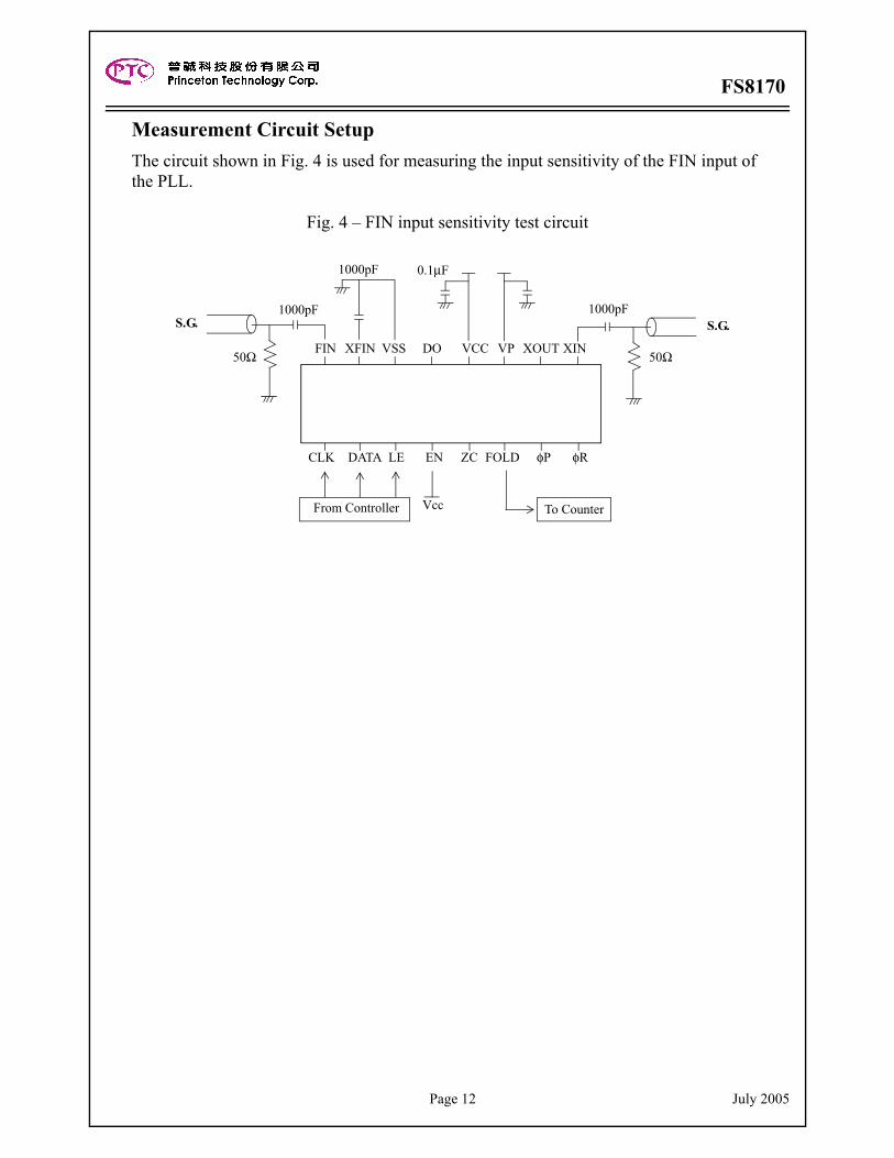
Measurement Circuit SetupThe circuit shown in Fig. 4 is used for measuring the input sensitivity of the FIN input of the PLL.
Fig. 4 – FIN input sensitivity test circuit
9 10 11 12 13 14 15 16
8 7 6 5 4 3 2 1
XINXOUTVPVCCDOVSSXFINFIN
φPFOLDZCENLEDATACLK φR
S.G. S.G.1000pF 1000pF
50Ω 50Ω
1000pF 0.1µF
From Controller Vcc To Counter
Page 12 July 2005
FS8170
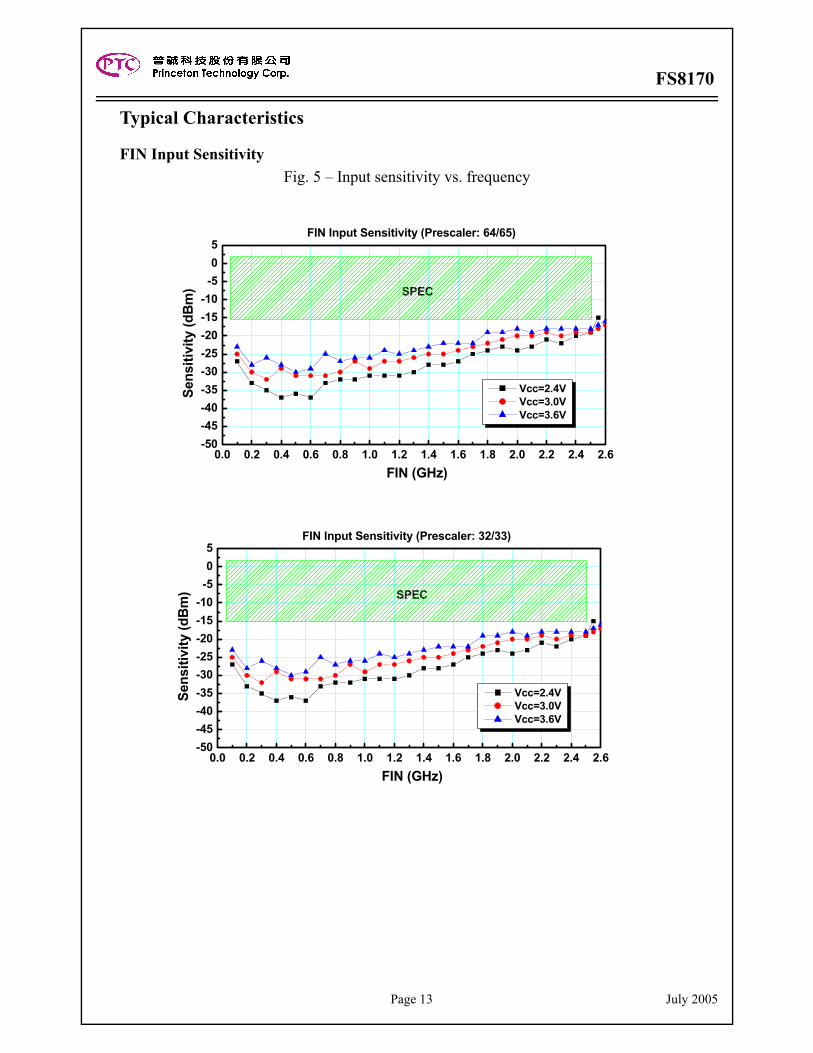
Typical Characteristics
FIN Input SensitivityFig. 5 – Input sensitivity vs. frequency
0.0 0.2 0.4 0.6 0.8 1.0 1.2 1.4 1.6 1.8 2.0 2.2 2.4 2.6-50-45-40-35-30-25-20-15-10-505
SPEC
FIN Input Sensitivity (Prescaler: 64/65)
Sens
itivi
ty (d
Bm
)
FIN (GHz)
Vcc=2.4V Vcc=3.0V Vcc=3.6V
0.0 0.2 0.4 0.6 0.8 1.0 1.2 1.4 1.6 1.8 2.0 2.2 2.4 2.6-50-45-40-35-30-25-20-15-10-505
Vcc=2.4V Vcc=3.0V Vcc=3.6V
SPEC
FIN Input Sensitivity (Prescaler: 32/33)
Sens
itivi
ty (d
Bm
)
FIN (GHz)
Page 13 July 2005
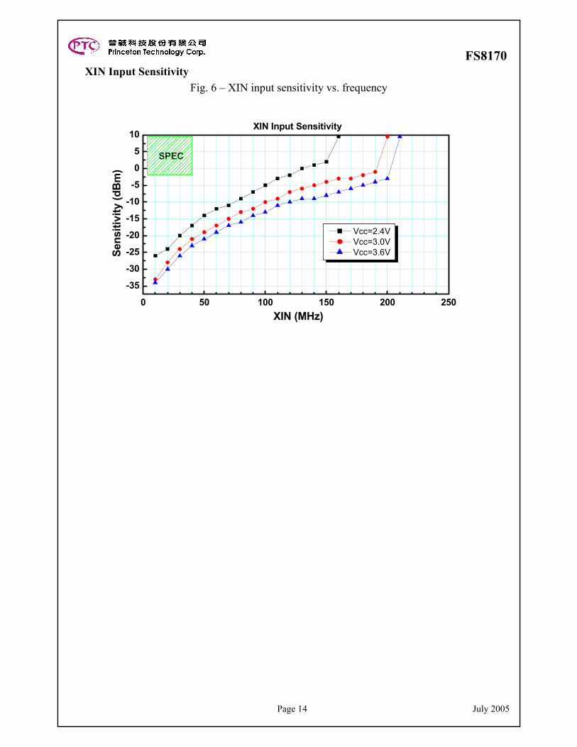
FS8170XIN Input Sensitivity
Fig. 6 – XIN input sensitivity vs. frequency
0 50 100 150 200 250
-35
-30
-25
-20
-15
-10
-5
0
5
10
SPEC
XIN Input Sensitivity
Se
nsiti
vity
(dB
m)
XIN (MHz)
Vcc=2.4V Vcc=3.0V Vcc=3.6V
Page 14 July 2005
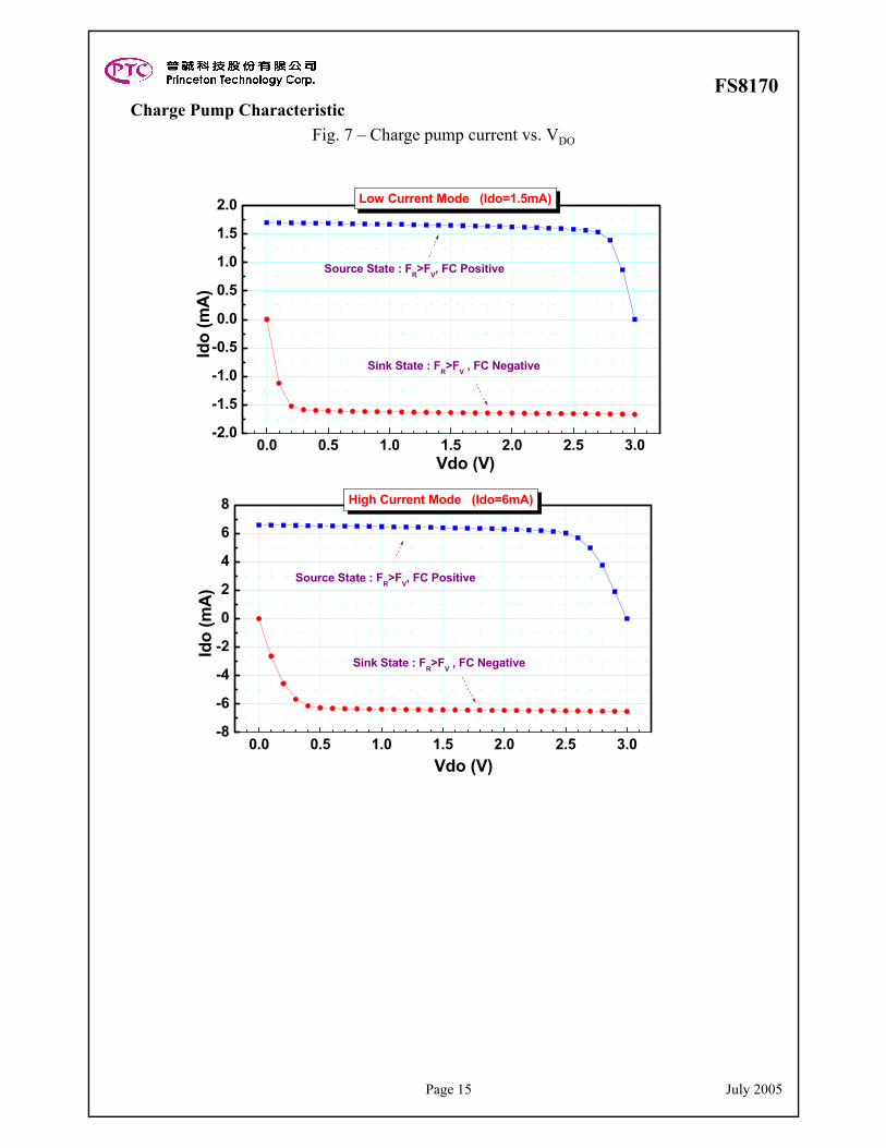
FS8170Charge Pump Characteristic
Fig. 7 – Charge pump current vs. VDO
0.0 0.5 1.0 1.5 2.0 2.5 3.0-8
-6
-4
-2
0
2
4
6
8
Sink State : FR>FV , FC Negative
Source State : FR>FV, FC Positive
High Current Mode (Ido=6mA)
Ido
(mA
)
Vdo (V)
0.0 0.5 1.0 1.5 2.0 2.5 3.0-2.0
-1.5
-1.0
-0.5
0.0
0.5
1.0
1.5
2.0
Sink State : FR>FV , FC Negative
Source State : FR>FV, FC Positive
Low Current Mode (Ido=1.5mA)
Id
o (m
A)
Vdo (V)
Page 15 July 2005
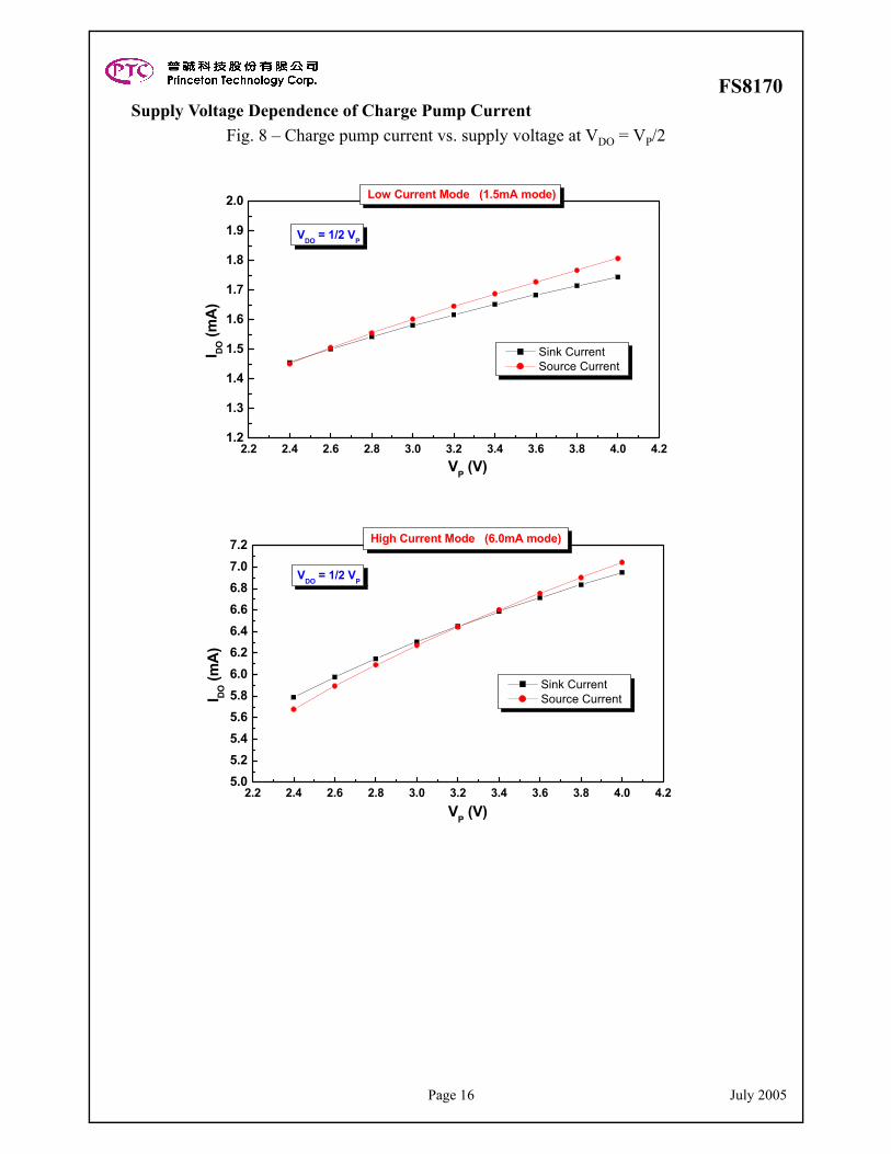
FS8170Supply Voltage Dependence of Charge Pump Current
Fig. 8 – Charge pump current vs. supply voltage at VDO = VP/2
2.2 2.4 2.6 2.8 3.0 3.2 3.4 3.6 3.8 4.0 4.21.2
1.3
1.4
1.5
1.6
1.7
1.8
1.9
2.0
Sink Current Source Current
Low Current Mode (1.5mA mode)
VDO = 1/2 VP
I DO (m
A)
VP (V)
2.2 2.4 2.6 2.8 3.0 3.2 3.4 3.6 3.8 4.0 4.25.05.25.45.65.86.06.26.46.66.87.07.2 High Current Mode (6.0mA mode)
VDO = 1/2 VP
I DO (m
A)
VP (V)
Sink Current Source Current
Page 16 July 2005
FS8170
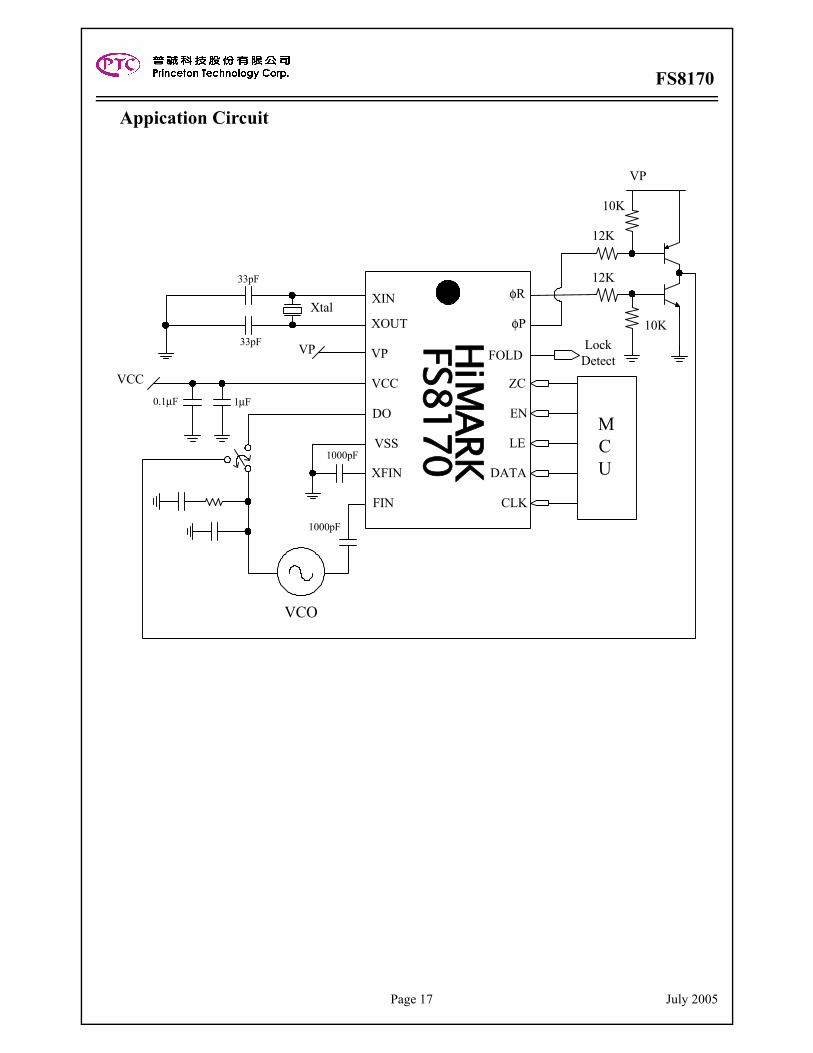
Appication Circuit
XtalXOUT
VP
VCC
DO
VSS
XFIN
FIN
φR
φP
FOLD
ZC
EN
LE
DATA
CLK
MCU
HiMARKFS8170
1000pF
12K
33pF
33pF
1µF
VCC
VCO
LockDetect
VP
VP
12K
10K
10K
XIN
1000pF
0.1µF
Page 17 July 2005