full-bridge dc-dc converter using asymmetric phase … · abstract: a novel zero-voltage ... load...
TRANSCRIPT

Send Orders for Reprints to [email protected]
The Open Automation and Control Systems Journal, 2015, 7, 1909-1915 1909
1874-4443/15 2015 Bentham Open
Open Access Full-Bridge DC-DC Converter Using Asymmetric Phase-Shifted PWM Control Tao Haijun*,1,2, Zhang Yiming1 and Ren Xiguo1
1College of Electronic Information and Control Engineering, Beijing University of Technology, Beijing 100124, P.R. China 2School of Electrical Engineering and Automation, Henan Polytechnic University, Jiaozuo, Henan, 454003, P.R. China
Abstract: A novel zero-voltage and zero-current switching (ZVZCS) Full-bridge converter is proposed using Asymmetric Phase-shifted PWM Control, Current in primary winding during the freewheeling period is reduced to zero by adding a blocking capacitor and a saturable inductor, realizing ZCS turn-on and ZVS turn-off for chopping-leg switches as well as ZCS turn-on and turn-off for lagging-leg switches. The control method is easy digital realization, overcomes control precision and flexibility of the traditional phase-shifting control special chip. The operation processes and characteristics of the converter are analyzed, and a prototype is built. Experimental results verify the proposed DC-DC converter with low freewheeling energy, low switching loss and high efficiency.
Keywords: Asymmetric phase-shifted, DC-DC converter, full-bridge, PWM, ZVZCS.
1. INTRODUCTION
Zero voltage switching (ZVS) full-bridge DC-DC converter has been received considerable attention for high-frequency power conversion to reduce the current and voltage stresses as well as the switching losses occurring in traditional hard switching PWM converters [1-3]. Metal-Oxide semiconductor field Transistors (MOSFET) are the power semiconductor devices of choice for this converter [4]. However, ZVS full-bridge converters have two major disadvantages: 1) a relatively large circulating current during the freewheeling interval results in power losses in the device and the transformer [5], 2) the dead time of the chopping leg switches is much higher than that of the lagging leg switches resulting in duty ratio loss [6]. To overcome the problem of the ZVS converter, a zero-voltage transition(ZVT) full-bridge converter is developed [7, 8], however the circuit is complexity since it requires two auxiliary switches and an additional resonant inductor [9, 10]. ZVZCS converter using a dc-blocking capacitor in series with a saturable inductor was present using phase-shifted PWM control [11-13]. The switches are operated under ZVS turn-on conditions ZCS turn-off conditions to minimize the freewheeling internal [14], the ZVZCS turn-on mechanism of the lagging leg switches is the same, however the ZCS turn-off mechanism of lagging leg switches consisting in applying a negative voltage to the transformer leakage inductance, so the switch current becomes zero before the gate signal forces the switch turn off [15]. A novel ZVZCS full-bridge converter is proposed in this paper. To achieve
ZCS of lagging-leg switches, a blocking capacitor with quite low capacitance is used and a small saturable inductor is added in the primary winding. ZVS for chopping-leg switches is achieved by outputting energies stored in the filter inductance. This is achievable within wide input and load range because external bulk capacitor can be added in the chopping-leg switches. During the freewheeling period, current in primary winding resets through the small blocking capacitor and keeps at zero. Since the saturable inductor blocks reverse current, ZCS is available to lagging-leg switches. Energies stored in the leakage inductance are transferred to the blocking capacitor and a wide control range of duty ratio can be gained by increasing voltage (reducing capacitance) of the blocking capacitor.
2. ZVZCS FULL-BRIDGE DC/DC CONVERTER
2.1. Topological Structure of the Proposed Converter
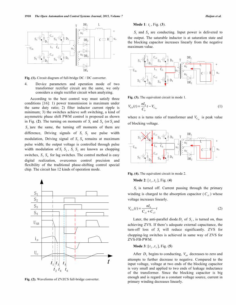
Circuit diagram of ZVZCS DC-DC converter is shown in Fig. (1). Left arm includes switches S1,S2 (including D1,D2 and Cs1,Cs2 ). Right arm includes switches S3,S4 (including D3 ~ D4 ). Ls is saturable inductor, Cb is dc-blocking capacitor.
2.2. Operating Process
To illustrate the steady-state operation, we made some rational assumptions, which are given below: 1. All components are ideal; 2. The inductance of the saturable inductor is infinite
when it is not saturated, and zero when it is saturated; 3. The output filter inductor is large enough to be treated
as a constant current source during a switching period.
1910 The Open Automation and Control Systems Journal, 2015, Volume 7 Haijun et al.
Udc
S1
S2
S3
S4
C
L
D1DR2 R
u1
u2+
-
uo
Ls Cb
Cs1
Cs2
D2
DR1
D3
D4
T
DR4
u2 DR3
Fig. (1). Circuit diagram of full-bridge DC / DC converter.
4. Device parameters and operation mode of two transformer rectifier circuit are the same, we only considers a single rectifier circuit when analyzing.
According to the best control way must satisfy three conditions [16]: 1) power transmission is maximum under the same duty ratio; 2) filter inductor current ripple is minimum; 3) the switches achieve soft switching, a kind of asymmetric phase shift PWM control is proposed as shown in Fig. (2). The turning on moments of S1 and S4 (or S2 and S3 )are the same, the turning off moments of them are difference, Driving signals of S1 S2 use pulse width modulation, Driving signal of S3 S4 remains at maximum pulse width; the output voltage is controlled through pulse width modulation of S1 S2 , S1 S2 are known as chopping switches, S3 S4 for lag switches. The control method is easy digital realization, overcomes control precision and flexibility of the traditional phase-shifting control special chip. The circuit has 12 kinds of operation mode.
S1S2
S3
S4
Uc
ip
UAB
2t3t4t
5t6t
1t t
Fig. (2). Waveforms of ZVZCS full-bridge converter.
Mode 1: t1 , Fig. (3).
S1 and S4 are conducting. Input power is delivered to the output. The saturable inductor is at saturation state and the blocking capacitor increases linearly from the negative maximum value.
Udc
S1
S2
S3
S4
C
LD1
DR2
Ru1
u2
u2
+
-
uoLs Cb
Cs1
Cs2
D2
DR1D3
D4
T
Fig. (3). The equivalent circuit in mode 1.
VCb (t) =nI0Cb
t −VCbp (1)
where n is turns ratio of transformer and VCbp is peak value of blocking voltage.
Udc
S1
S2
S3
S4
C
LD1
DR2
Ru1
u2
u2
+
-
uoLs Cb
Cs1
Cs2
D2
DR1D3
D4
T
Fig. (4). The equivalent circuit in mode 2.
Mode 2: [ t1 , t2 ], Fig. (4)
S1 is turned off. Current passing through the primary winding is charged to the absorption capacitor (Cs1 ) whose voltage increases linearly.
VCs1(t) =nI0
Cs1 +Cs3
t (2)
Later, the anti-parallel diodeD3 of S3 , is turned on, thus achieving ZVS. If there’s adequate external capacitance, the turn-off loss of S1 will reduce significantly. ZVS for chopping-leg switches is achieved in same way of ZVS for ZVS-FB-PWM.
Mode 3: [ t2 , t3 ], Fig. (5)
After D3 begins to conducting, Vab decreases to zero and attempts to further decrease to negative. Compared to the input voltage, voltage at two ends of the blocking capacitor is very small and applied to two ends of leakage inductance of the transformer. Since the blocking capacitor is big enough and is regard as a constant voltage source, current in primary winding decreases linearly.

Asymmetric Phase-Shifted PWM Control The Open Automation and Control Systems Journal, 2015, Volume 7 1911
I p (t) = −VCbpLlk
t + nI0 (3)
Udc
S1
S2
S3
S4
C
LD1
DR2
Ru1
u2
u2
+
-
uoLs Cb
Cs1
Cs2
D2
DR1D3
D4
T
Fig. (5). The equivalent circuit in mode 3.
So, the energy stored in the leakage inductance is recovered to the blocking capacitor. The difference between the primary current reflected to the secondary and the current in the filter inductor freewheels through the secondary rectifier. The saturable inductor is still saturated.
Udc
S1
S2
S3
S4
C
LD1
DR2
Ru1
u2
u2
+
-
uoLs Cb
Cs1
Cs2
D2
DR1D3
D4
T
Fig. (6). The equivalent circuit in mode 4.
Mode 4: [ t3 , t4 ], Fig. (6)
When current in primary winding reduces to 0, it will attempt to further reduce to negative. Such attempt is stopped by the recovery of saturable inductor from saturation state, which keeps current in primary winding at 0. Therefore, all voltages of the blocking capacitor are applied to the saturable inductor. Voltage of the blocking capacitor remains constant. S4 achieves ZCS turn-off.
Udc
S1
S2
S3
S4
C
LD1
DR2
Ru1
u2
u2
+
-
Ls Cb
Cs1
Cs2
D2
DR1D3
D4
T
Fig. (7). The equivalent circuit in mode 5.
Mode 5: [ t4 , t5 ], Fig. (7)
Four switches are all turned off during the dead time of switches. Due to leakage inductance of transformer and effect of saturable inductor, current in primary winding of the transformer is kept zero and voltage of the blocking capacitor remains unchanged. The secondary rectifier diodes
are all opened and the voltage in secondary winding of the transformer is zero.
Udc
S1
S2
S3
S4
C
LD1
DR2
Ru1
u2
u2
+
-
uoLs Cb
Cs1
Cs2
D2
DR1D3
D4
T
Fig. (8). The equivalent circuit in mode 6.
Mode 6: [ t5 , t6 ], Fig. (8)
S2 and S3 are turned on. Since current in primary winding couldn’t be changed suddenly, the saturable inductor fails to reach saturation in short switching time. ZCS is achieved and the saturable inductor reaches saturation quickly. The high voltage (sum of input voltage and peak voltage of the blocking capacitor) on two ends of the inductance will be applied on two ends of the leakage inductance after the saturable inductor reached saturation. Current in primary winding increases linearly to converted output current.
I p (t) =Vdc +VCbp
Llkt (4)
This is the end of an operating half period, an operating full cycle includes two of such half operating cycle. The proposed circuit achieves ZCS turn-on and ZVS turn-off for advance bridge arm as well as ZCS for lagging bridge arm.
3. FEATURES OF THE PROPOSED CIRCUIT
3.1. Maximum Controlled Duty Ratio
The maximum duty ratio of ZVZCS full-bridge converter is determined by three parameters. It can be seen from Fig. (9) that the maximum duty ratio can be expressed as:
Dmax = 1−td + ΔT +TZC
T / 2 (5)
where td is the time period of Mode 2; ΔT is the time period of Mode 3; and TZC is the time period of Mode 5.
ZVS mechanism of chopping-leg switches is same with that of ZVS full-bridge converter. To reduce turn-off loss and external capacitance of IGBT, the equivalent switch capacitance of the chopping-leg switches increases. ZVS range of the ZVZCS full-bridge converter is limited significantly. The desired dead time to keep ZVS between chopping-leg switches is:
td =VdcCs1 +Cs3
nI0 (6)

1912 The Open Automation and Control Systems Journal, 2015, Volume 7 Haijun et al.
S4/S3
S1/S2
Is
Us
T/2dt TΔ ZCT t
Fig. (9). Simplified waveform of primary voltage and current.
During underloading, t d increases and the maximum duty ratio decreases. Reset time of current in primary winding ( ΔT ) is another parameter that determines the maximum duty ratio. If the blocking capacitor has adequate voltage, it can be viewed as a constant voltage source. In Mode 3, ΔT can be expressed as:
ΔT = nI0LlkVCbp
(7)
where VCbp is peak voltage of the blocking capacitor:
VCbp =nI0DT4Cb
(8)
Simplify (7) and (8)
ΔT = 4LlkCb
DT (9)
According to (9), ΔT is independent from load current, but is inversely proportional to the duty ratio. To maximize control range of duty ratio, leakage inductance shall be minimized. However, the blocking capacitor couldn’t be shrunk unlimitedly because its peak voltage increases. As a result, circulating energies on the leakage inductance and blocking capacitor shall be increased and the saturable inductor shall be enlarged, which will cause considerable magnetic core losses. Therefore, the maximum control range of duty ratio, size of blocking capacitor and size of saturable inductor shall be balanced according to practical applications.
TZC is the dead time of lower IGBT on-off control on the lagging bridge arm, which shall be longer than the service life of IGBT minority carrier to avoid simultaneous turning on of upper and lower leg switches.
3.2. Switching Loss
1) ZCS turn-on and ZVS turn-off for the chopping-leg switches
The chopping-leg switch adopting ZCS turn-on has zero turn-on loss (Fig. (10a). Since there’s tail current during IGBT turn-off, voltage at two ends of the switch and current passing through the switch overlap, thus causing switching loss. Voltage at two ends of the switch during the turn-off process depends on absorption capacitance of leg switch and current passing through it. These determine the rate of rise (dV / dt ) of the switching voltage. dV / dt can be reduced through the parallel external absorption capacitance of the switches, which, however, will influence the maximum controlled duty ratio. 2) ZCS for lagging-leg switches For lagging-leg switches, the saturable inductor breaks away from saturation before the IGBT is turned on and current passing through IGBT decreases to zero. In this way, no turn-on loss is generated and ZCS turn-on is achieved (Fig. (10b). When the IGBT is turned off, current in primary winding still maintains at zero since the saturable inductor won’t reach saturation immediately, thus enabling the lagging-leg switches to realize ZCS turn-off. Moreover, low-speed IGBT with small tail current still can be served in high-frequency environment as long as there’s adequate long freewheeling period and most minority carriers can be recombined.
UsIs
UsIs
UsIs
UsIs
(a)
(b)Turn on
Turn offTurn on
Turn off
Fig. (10). ZVZCS waveform for IGBT’s (a) ZVS and ZCS of chopping-leg switches (b) ZCS of lagging-leg switches.
3.3. Efficiency
To achieve ZVS for the lagging-leg switches, current in primary winding at leakage inductance has to be kept at reflected output current in primary winding during the whole freewheeling period of ZVS full-bridge converter. This means that most reflected output currents flow through the primary winding (Fig. 11a). The circuit efficiency during the freewheeling period is low, which is caused by the turn-on losses of two switches in primary winding and the transformer. Additionally, big leakage inductance is needed to get a reasonable ZVS range, which will cause duty ratio loss. Consequently, the overall circuit efficiency will further

Asymmetric Phase-Shifted PWM Control The Open Automation and Control Systems Journal, 2015, Volume 7 1913
decrease. In the ZVZCS full-bridge converter, follow current in primary winding decreases significantly (Fig. (11b) and the duty ratio loss can be neglected. Needing no big leakage inductance, the saturable inductor reaches saturation quickly when transferring energies from the primary winding to the seconding winding. The secondary rectifier voltage of ZVZCS full-bridge converter is not a square wave, but its average voltage is same as that of ZVS full-bridge converter.
(a)
(b)
UAB
U2
Ip
UAB
U2
Ip
Fig. (11). Comparison of waveforms of the primary voltage and current and secondary rectifier voltage (a) ZVS-FB-PWM circuit (b) ZVZCS-FB-PWM circuit.
4. EXPERIMENTAL RESULTS
A prototype of the proposed ZVZCS full-bridge DC-DC converter has been built to verify the principle of operation. The prototype converter has the following specification:
Dc bus voltage: Vdc = 540Vw .
Output voltage: Vo = 30V .
Output current: Io = 200A .
Switching frequency: fs = 20kHz .
Driving signals of four IGBTs of the inverter bridge in the full-bridge DC/DC converter are shown in Fig. (12). The chopping-leg switches and lagging-leg switches are turned on simultaneously but turned off at different time. The driving signals of the chopping-leg switches adopt PWM, while those of the lagging-leg switches keep at maximum, thus implementing power regulation within a wide load range. Output voltage waveform of the inverter bridge, waveform of voltage in primary winding of the transformer, waveforms of voltages at two ends of the lagging-leg switches and waveform of current in primary winding of the transformer are displayed in Fig. (13). These waveforms are in good accordance with theoretical analysis. ZCS is available to the lagging bridge arm. Current in primary winding during the follow current period decreases significantly. There’s a sudden change on the voltage
waveform of the transformer. This is caused by the IGBT parasitic capacitance on the lagging bridge arm.
Fig. (12). Four drivers wave for PWM inverter bridge.
Fig. (13). Primary and secondary voltage and current waveforms.
Waveforms of voltage at two ends of the chopping-leg switches and waveform of current in primary winding of the transformer are shown in Fig. (14). The chopping-leg switches adopt ZCS turn-on and ZVS turn-off. Slopes of rising edge and falling edge are determined by the shunt capacitance, without sudden change like that on the lagging-leg switches.
Fig. (14). Chopping-leg voltage and primary current waveforms.

1914 The Open Automation and Control Systems Journal, 2015, Volume 7 Haijun et al.
Waveforms of voltage and current in primary winding of the transformer in ZVZCS full-bridge converter and ZVS full-bridge converter are shown in Figs. (15, 16), respectively. Experimental results are consistent with theoretical analysis. The proposed ZVZS converter presents significantly lower circulating energies.
Fig. (15). Primary voltage and current waveforms in ZVZCS mode.
Fig. (16). Primary voltage and current waveforms in ZVS mode.
Measure efficiencies of the proposed ZVZCS full-bridge converter and the traditional ZVS full-bridge converter are exhibited in Fig. (17). The maximum overall efficiency of the proposed converter is 95%, while that of the traditional converter is 93%.
CONCLUSION
The Novel ZVZCS full bridge DC-DC converter adding a dc-blocking capacitor and saturable inductor using Asymmetric Phase-shifted PWM Control improves the power density and performance in high power application. The operation process is presented in detail and characteristics of the circuit are analyzed. The 6kW prototype is built using IGBT’s at 20kHz switching frequency. The proposed converter using asymmetric phase-shifted PWM control has the following advantages over the
traditional ZVZCS using symmetric Phase-shifted PWM Control: 1) The chopping-leg switches of the proposed converter
turn on under ZCS conditions and turn off under ZVS conditions, the lagging-leg switches turn on and turn off under ZCS conditions. The chopping-leg switches of the traditional converter turn on and turn off under ZVS conditions, the lagging-leg switches turn on under ZVS conditions and turn off under ZCS conditions. The proposed converter reduces the switching loss and improves the efficiency.
2) Asymmetric phase-shifted PWM control is easy digital realization, overcomes control precision and flexibility of the traditional phase-shifting control special chip.
Fig. (17). Measure efficiency of the proposed ZVZCS converter and the traditional converter.
CONFLICT OF INTEREST
The authors confirm that this article content has no conflict of interest.
ACKNOWLEDGEMENTS
Authors wishing to acknowledge assistance or encouragement from colleagues, financial support by R&D of Key Instruments and Technologies for Deep Resources Prospecting (the National R&D Projects for Key Scientific Instruments), GrantNo. ZDYZ2012-1-05-01.
REFERENCES [1] X. Zhang, and W. Chen, “A novel ZVS PWM phase-shifted full-
bridge converter with controlled auxiliary circuit,” Transactions of China Electrotechnical Society, vol. 25, pp. 81-88, 2010.
[2] W. Jiang, and R. Hu, “ZVS condition of symmetry half-bridge converter with phase-shifted control,” Transactions of China Electrotechnical Society, vol. 26, pp. 8-13, 2011.
[3] M. J. Baei, and M. M. Narimani, “A new ZVS-PWM full-bridge boost converter,” Journal of Power Electronics, vol. 14, pp. 237-248, 2014.
[4] X. Wu, J. Zhang, X. Xie, and Z. Qian, “Analysis and optimal design considerations for an improved full bridge ZVS DC-DC converter with high efficiency,” IEEE Transactions on Power Electronics, vol. 21, pp. 1225-1234, 2006.
[5] M. D. Cruz, Castaldo, and C. Fernando, “Application of the ZVS-PWM commutation cell to a full-bridge DC-DC converter,” IEEE
0
0.1
0.2
0.3
0.4
0.5
0.6
0.7
0.8
0.9
1
40 60 80 100 120 140 160 180 200/A
Proposed
Traditional

Asymmetric Phase-Shifted PWM Control The Open Automation and Control Systems Journal, 2015, Volume 7 1915
Transactions on Circuits and Systems I: Fundamental Theory and Applications, vol. 46, pp. 379-388, 1999.
[6] Y. Jang, and M. M. Jovanovic, “A new PWM ZVS full-bridge converter,” IEEE Transactions on Power Electronics, vol. 22, pp. 987-994, 2007.
[7] C. S. Yun, B. C. Kim, K. H. Kim, Y. C. Lim, and P. Freere, “Reducing the high frequency transformer losses in an FB ZVT PWM converter,” IEE Proceedings: Electric Power Applications, vol. 149, pp. 161-164, 2002.
[8] H. F. Xiao, X, P. Liu, and K. Lan, “Zero-voltage-transition full-bridge topologies for transformerless photovoltaic grid-connected inverter,” IEEE Transactions on Industrial Electronics, vol. 61, pp. 5393-5401, 2014.
[9] B. Su, L. J. Hang, T. Yang, Z. W. Yang, Z. Y. Lu, and Z. M. Qian, “Novel single-stage isolated ZVT power-factor-corrected converter,” In: Proceedings of the Chinese Society of Electrical Engineering, vol. 28, pp. 40-46, 2008.
[10] T. C. Sun, P. H. Tang, P. Gao, and H. P. Liu, “Novel full-bridge ZVT PWM DC-DC converter,” In: Proceedings of the Chinese Society of Electrical Engineering, vol. 26, pp. 83-88, 2006.
[11] J. Yao, Y. Zhang, and J. Liu, “Full-bridge phase-shift PWM ZVZCS converter,” Electric Power Automation Equipment, vol. 30, pp. 66-70, 2010.
[12] M. Pahlevaninezhad, P. Das, J. Drobnik, P. K. Jain, A. Bakhshai, “A novel ZVZCS full-bridge DC/DC converter used for electric vehicles,” IEEE Transactions on Power Electronics, vol. 27, pp. 2752-2769, 2012.
[13] X. Wu, X. Xie, C. Zhao, Z. Qian, and R. Zhao, “Low voltage and current stress ZVZCS full bridge DC-DC converter using center tapped rectifier reset,” IEEE Transactions on Industrial Electronics, vol. 55, pp. 1470-1477, 2008.
[14] D. S. Wijeratne, and G. Moschopoulos, “A ZVS-PWM full-bridge converter with reduced conduction losses,” IEEE Transactions on Power Electronics, vol. 29, pp. 3501-3513, 2014.
[15] E. H. Kim, and B. H. Kwon, “Zero-voltage- and zero-current-switching full-bridge converter with secondary resonance,” IEEE Transactions on Industrial Electronics, vol. 57, pp. 1017-1025, 2010.
[16] Y. Ma, X. Ruan, and L. Zhou, “The best modulation strategy of the full-bridge three-level converter,” In: Proceeding of the CSEE, vol. 23, pp. 111-116, 2003.
Received: September 16, 2014 Revised: December 23, 2014 Accepted: December 31, 2014
© Haijun et al. Peng; Licensee Bentham Open.
This is an open access article licensed under the terms of the (https://creativecommons.org/licenses/by/4.0/legalcode), which permits unrestricted, non-commercial use, distribution and reproduction in any medium, provided the work is properly cited.