fully printed and flexible memristors for self- sustainable · pdf filefully printed and...
TRANSCRIPT

Tampere University of Technology
Fully printed memristors for a self-sustainable recorder of mechanical energy
CitationVilmi, P., Nelo, M., Voutilainen, J-V., Palosaari, J., Pörhönen, J., Tuukkanen, S., ... Fabritius, T. (2016). Fullyprinted memristors for a self-sustainable recorder of mechanical energy. Flexible and Printed Electronics, 1(2),[025002]. DOI: 10.1088/2058-8585/1/2/025002Year2016
VersionEarly version (pre-print)
Link to publicationTUTCRIS Portal (http://www.tut.fi/tutcris)
Published inFlexible and Printed Electronics
DOI10.1088/2058-8585/1/2/025002
CopyrightThis is an author-created, un-copyedited version of an article accepted for publication in Flexible and PrintedElectronics. The publisher is not responsible for any errors or omissions in this version of the manuscript or anyversion derived from it. The Version of Record is available online at http://dx.doi.org/10.1088/2058-8585/1/2/025002.
Take down policyIf you believe that this document breaches copyright, please contact [email protected], and we will remove access tothe work immediately and investigate your claim.
Download date:18.05.2018

Fully printed and flexible memristors for self-
sustainable recorder of mechanical energy
Pauliina Vilmi1*, Mikko Nelo2, Juha-Veikko Voutilainen1, Jaakko Palosaari2, Juho Pörhönen3,
Sampo Tuukkanen3,4, Heli Jantunen2, Jari Juuti2 and Tapio Fabritius1
1Optoelectronics and Measurement Techniques Laboratory, University of Oulu, FI-90014, Oulu,
Finland
2Microelectronics and Materials Physics Laboratories, University of Oulu, FI-90014, Oulu, Finland
3 Department of Electronics and Communications Engineering, Tampere University of Technology,
P.O.Box 692, FI-33101, Tampere, Finland
4Present address: Department of Automation Science and Engineering, Tampere University of
Technology, P.O.Box 692, FI-33101, Tampere, Finland
*Corresponding author: Pauliina Vilmi, e-mail: [email protected]
Keywords: inkjet printing, memristor, printed electronics, titanium-oxide, TiOx, piezoceramic
1

Abstract
Memristors have attracted significant interest in recent years, because of their role as a missing
electronic component and unique functionality that has not previously existed. Since the first
discoveries of existence of memristive materials, various different fabrication processes for
memristors have been presented. Here a simple additive fabrication process is demonstrated: the
first fully printed and flexible memristors were deposited on polymer substrate by using
conventional inkjet printing technique. The memristor structure was printed on a 125 µm thick
polyethylene terephthalate (PET) substrate by sandwiching a thin layer of TiOx between two silver
nanoparticle ink electrodes. Current-Voltage (IV) characterization measurements were performed
and they showed clear memristive behavior when voltage pulse amplitude varied between -1.5 V
and 1.5 V. The corresponding resistance change is approximately between 150 Ω and 75 kΩ. In
order to demonstrate switching scheme in practical application printed memristors and printed
voltage doubler were connected with piezoelectric element. The element was subjected to impact
type of excitation thus producing electric charge that was able to switch the memristor between high
and low resistive states. Results pave a way for an exploitation of cost efficient, self-sufficient, all–
printable memory elements for wide utilization in future electronics applications.
1. Introduction
Since the invention of the memristor was predicted in 1971 1, it has been increasingly studied.
However, the first memristor saw the daylight in 2009 when Strukov et al. 2 presented their two-
terminal electrical device that behaves like a memristor. The late discovery is due to the fact that
memristive behavior arises only at nanoscale structures, which implementation has been difficult
earlier. Since then the research around it has been vigorous, as with such a memory element,
smaller, more efficient and low power consumption components can be made. Low power
consumption is due to the fact that a memristor does not need applied current to keep the memory
2

state, only to change it. It is even accompanied in artificial intelligence studies, because of its
neuron-like behavior 3, 4
. Other possible applications for this type of component are non-volatile
memories 5 and logic operations
6.
The basic structure of a memristor has two conductive elements with a thin dielectric layer between
them. When electric current is applied in one direction of the component the resistivity of the
dielectric layer increases and when the current is reversed the resistance decreases. The memristive
switching is believed to be due to the transport of oxygen vacancies and ions in the active layer of
the memristive element 5.
Previous development of memristor fabrication methods has been mainly focused on techniques
based on nanoimprint lithography (NIL) 7, 8
. Recently, also an electrohydrodynamic (EHD) inkjet
printing system has been used as a fabrication method. Duraisamy et al. 9 presented a process
where a bottom Cu electrode and top Ag electrode were fabricated by EHD printing and the TiO2
layer between was sprayed with EHD atomization. However, they used silicon substrate in their
memristors making them rigid. Choi et al. 10
also used EHD printing for the electrodes (both silver),
but the active ZnO layer was applied by spin coating. Recently Zou et al. 11
presented a printed
memristor, which had inkjet-printed silver top and bottom electrodes, but the memristive layer was
electroplated copper. A purely printed memristor on a flexible substrate has not yet been made. In
order to simplify the fabrication process and reduce the costs, the development of fully printed
memristors is desired.
In our earlier paper a memristive layer based on a TiOx precursor was developed for inkjet
printing12
, but the electrodes were fabricated using conventional methods. In this work, a process
for a fully inkjet-printed memristor is presented. The work is done with a “traditional” inkjet printer
with a piezo printing head. The piezo inkjet printer was chosen for its high resolution and digital
3

pattern control. It is worth of mention that all needed materials can be simply printed by one
equipment.
2. Materials and Methods
The inkjet printable formulation of the active layer material was prepared in-house. Other printable
materials are purchased as ready-to-use solutions. The synthesis of a TiOx –precursor solution is
presented in detail in previous publication 12
. In short, synthesis is based on the works of Kim et al.
13 and Gergel-Hackett et al.
14. Instead of using titanium (IV) isopropoxide as in the references,
titanium-di-isopropoxide-2-acetoacetate (75 wt. % of isopropanol, Aldrich, 13.2 mL) was prepared
as a precursor by mixing it with 2-methoxyethanol (99.3 %, Aldrich, 50 mL) and ethanolamine (99
%, Aldrich, 5 mL). The reagents were added to the reaction flask and flushed with nitrogen flow for
two minutes in order to remove oxygen from the reaction solution. Then, the stirred solution was
heated to 80 °C for 2 h, 120 °C for 1 h, followed by 80 °C for 2 h and 120 °C for 1 h as in Ref. 13
.
The resulting solution was collected, cooled and stored in a refrigerator at 5 °C. A solution for
inkjet-printing was prepared by diluting the TiOx -precursor with isopropyl alcohol (99.5 %, Lab-
Scan).
2.2. Printing
Fujifilm Dimatix materials printer DMP-2800, with a 10 pl cartridge was used to fabricate the
memristor. The structure has top and bottom silver electrodes and a thin layer of TiOx between
them. Figure 1 a) shows an illustration of the printed structure, one from top and one cross-section.
Printing was done on a polyethylene terephthalate (PET) substrate, which was cleaned with
isopropanol and kept in an oven at 150 °C for a few hours to shrink it. The pre-treatment was used
to obtain better temperature stability for the substrate over the fabrication process. The bottom
electrode was printed first on the pre-treated substrate. Electrodes were made of silver nanoparticle
4

ink (Sigma-Aldrich). One-millimeter-wide lines with one millimeter spacing were printed and
sintered in the oven at 150 °C for 20 min. In the next step, to achieve small enough active area, a
photoresist barrier was printed on the bottom electrode to define a circular shaped area of
approximately 60 µm in diameter. The photoresist pattern was hardened via the following steps:
pre-bake at 85 °C for 10 min, exposure (λ=365 nm) for 15 s and post-bake at 95 °C for 5 min.
The active layer (TiOx) was printed into the photoresist holes. All nozzles with a 40 V
operating voltage were used. The printed active layer was kept in air at room temperature for one
hour in order to let the precursor material hydrolyze into the desired TiOx end product. The
hydrolysis reactions were terminated by heating the printed sample in the oven with a nitrogen
atmosphere for 15 minutes at 150 ˚C. The top electrodes were printed on top to cover the active
area. The top electrode was sintered in the same way as the bottom electrode, except in the nitrogen
atmosphere to assure that the active layer will not become overly oxidized. Figure 1 b) shows the
printed photoresist pattern and an all-printed memristor device.
Figure 1. a) Illustration of the memristor structure. b) Image of a printed photoresist pattern on a
silver electrode and a microscope image of an all-printed memristor.
5

This kind of structure was chosen to eliminate possible short-cuts between silver contacts. In
the cross-bar structure there is a problem of having unwanted contact between silver wires. The
photoresist acts as an insulator barrier preventing electric breakdowns.
The layer structure of the memristors was studied by taking a cross-section cut from the
middle with a focused ion beam (FEI Helios FIB) and it was then examined with a scanning
electron microscope (SEM). Memristive behavior was measured with the Keithley 4200
semiconductor analyzer.
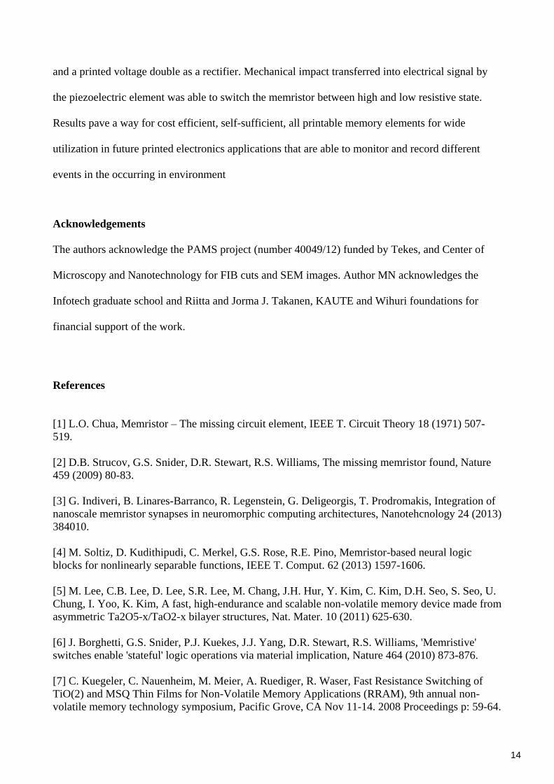
Ability to change the state of memristors with 5 µm drop spacing (Figure 2) was tested with
an electrical charge pulse. Pulses were created by dropping a weight on a piezoelectric element
(PZT-5H, Morgan Electro Ceramics). Piezoelectric disc of 35 mm in diameter and 0.50 mm in
thickness was placed between metal plates and compressed by dropping different size weights (101
g, 71 g and 36 g) from 0.75 meters. Electrical charge generated from piezoelectric material was
guided through a printed voltage doubler circuit to the memristor under test.
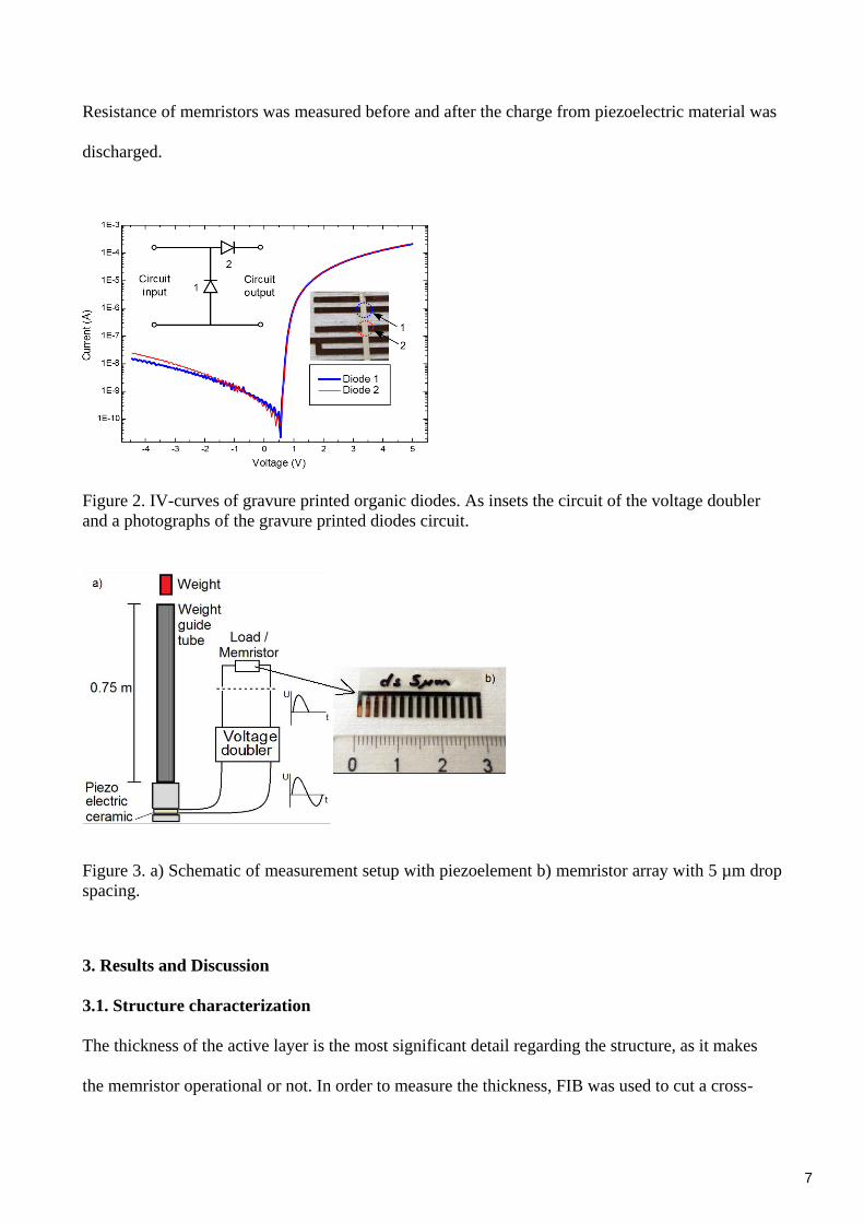
The printed voltage doubler rectifier circuit was composed of two organic gravure printed
Schottky diodes on Melinex ST506 PET substrate, as described in earlier work [15]. Diode cathode
was a 100 nm thick copper track deposited using Leybold 560 electron beam coater. Semiconductor
printed on the copper was 12.5 % poly(triarylamine) (PTAA) paste from Merck Chemicals Ltd.
Diode anode printed on top was Acheson Electrodag PM-460A paste from Henkel. Diodes were
characterized using Keithley 236 source-measure unit. The developed gravure printed organic
diodes has very good electrical performance, i.e. a low turn-on voltage and a rectification ratio as
high as 105 [16]. The typical IV-curves of printed diodes and a voltage doubler circuit are shown in
Figure 2.
A schematic view of the measurement setup is shown in Figure 3. Electrical pulses from the
piezoelectric disc were monitored simultaneously with Agilent 3000X series oscilloscope.
6
Resistance of memristors was measured before and after the charge from piezoelectric material was
discharged.
Figure 2. IV-curves of gravure printed organic diodes. As insets the circuit of the voltage doubler
and a photographs of the gravure printed diodes circuit.
Figure 3. a) Schematic of measurement setup with piezoelement b) memristor array with 5 µm drop
spacing.
3. Results and Discussion
3.1. Structure characterization
The thickness of the active layer is the most significant detail regarding the structure, as it makes
the memristor operational or not. In order to measure the thickness, FIB was used to cut a cross-
7

section of the structure. It was then examined with SEM. From the images the thicknesses of the
electrodes and the TiOx layer can be seen. Figure 4 shows the SEM image, where the thick dark
area on the bottom is the PET substrate, the Ag bottom electrode is above PET, TiOx layer is the
thin dark area and above that is the Ag top electrode. The TiOx layer is thickest at about 160 nm and
it is progressively thinner toward the other edge to approximately 10 nm. Assumingly, the current
flows through the thinnest part, which would be at the 10-nm-thick area. One would assume that for
a memristor to function optimally the layer should be uniform all over. This is something to
consider for the future optimization of the structure. One other notable thing is the difference
between the two silver electrodes. The bottom electrode has been baked twice at 150 °C for 20 min
and the top electrode is baked only once, so the bottom electrode is sintered more, thus its
microstructure is different. There is also an issue with the compatibility of TiOx and silver. When a
functional memristor was studied with FIB and SEM for four weeks after the measurements, the
active layer was not visible any more. It appears that silver diffuses to TiOx over time. This is
obviously the main limitation to component lifetime at this moment.
Figure 4. SEM image of a FIB cross-section of the memristor.
8

3.2. Functionality tests
The electrical I-V characterization of the memristors was performed with the Keithley 4200
semiconductor analyzer. The measurements were done partly with the in-house built multiplexer
board and partly with direct probing. The multiplexer measurement board enables the measurement
of several memristors consecutively without an external probing system. The measurement board is
based on the ECIO 28P microcontroller, which controls the multiplexer. The multiplexer, on the
other hand, selects the memristor to be measured from the total of 14 memristors in one substrate.
Direct probing was done to confirm that the multiplexer board does not add any error to the
measurements. It was concluded that the multiplexer board adds approximately 4 series
resistance (mux path resistance), but does not otherwise affect to the measurements.
The fabricated memristors were characterized for their functionality by pulsing them with
consecutive rising and falling pulse amplitudes with the triangular shape pattern illustrated in Figure
5. The pulse on-time and off-time were kept constant, i.e. 5 ms and 100 ms, respectively. The pulse
amplitude was increased or decreased in 0.1 V steps until the shift from high to low resistance state
was observed. The measurements were performed before the falling edge of the writing pulse.
Figure 5. The memristor test amplitude sequence.
9

A clear memristive behavior was observed, when the memristor resistance suddenly dropped
from a high resistance to a low resistance state during the rising writing pulse amplitudes. The re-
writing to high resistance state was observed when amplitudes of negative pulses were increased for
already written memristor.
In Figure 6, the I-V and R-V curves of a functional memristor are presented. From Figure 6 a), it is
clearly seen that the memristive shift from low conductance to high conductance state happens in the region
of 1.5 V pulse amplitude. The back writing occurs similarly, approximately at -1.5 V pulse amplitude. In
Figure 6 b) the resistance dependence from the pulse amplitude is depicted. The resistance shifts from
approximately 75 k to 150 and back. This occurred during almost three writing cycles. The first two
cycles are quite similar and have fast changes from one state to another. The third cycle also changed its
state, but at a lower voltage (around 1 V). The back writing is not clearly as good as with previous cycles,
only a small, irregular loop was created. In the resistance Figure 6 b) the third cycle requires four steps to
achieve the same resistance than the previous cycles.
Figure 6. The a) I-V and b) R-V behavior of the functional memristor.
Several memristors are tested and it seems that functional memristors exhibit quite large initial high
resistance state. A lower initial resistance indicates a thinner TiOx layer making a memristor more
10

vulnerable to electrical breakthrough. Also, too small initial resistance might lead to the saturation
of the measurement apparatus test current (current limit 0.1 A) after phase shift from high to low
resistance. From a physical structure point of view one possible reason for the breakdown at early
stage might be the thickness variation of the TiOx layer, which was seen in Figure 4. If there are
very thin areas (10 nm) and a 1.5 V voltage is applied, it generates electric field of 75 V/µm for the
memristor material. Such electric field is already close to the dielectric breakdown strength of a
high quality SiO2 film and above that of presented for amorphous doped TiOx capacitor films 15
.
For future studies, the fabrication process should be stabilized and optimized for better yield.
The main focus should be on the active layer and deposition of it. The layer should be as uniform as
possible or perhaps barrier layers could be made between the active layer and the silver contacts, to
eliminate the diffusion.
3.3. Voltage doubler
Printed voltage double rectifier circuit was first tested without the memristor to analyze the
functionality of the rectifier and also, to find out the amplitude of the pulse charges obtained from
the piezoceramic component which is important as the memristor electrical load is altered by pulse
current. Electrical pulse from the piezoceramic was guided through printed rectifier and over a 1 kΩ
load. Figure 7 illustrates operation of the rectifier and charge amplitudes as weights of 36 g, 71 g,
and 101 g were dropped from 0.75 m onto the piezoelectric ceramic. Printed rectifier worked as
expected and prohibited the negative voltage from flowing through the circuit. By switching the
connections vice versa only negative voltage was obtained and positive filtered out. Charges
generated by piezoelectric element resulting from the three masses were calculated as 0.37 µC, 2.06
µC and 3.14 µC respectively.
11

Figure 7. Voltage pulses through voltage doubler rectifier and over a 1 kΩ load from piezoelectric
element. 36 g mass was used to produce the green pulse, 71 g mass for the red pulse and 101 g mass
for the purple pulse.
3.4. Piezo tests
Memristors were tested by driving both positive and negative polarity pulses over them. All
memristors shifted to a smaller electrical resistance with pulses of negative polarity. Negative and
positive pulses had to be over the smallest charge of 0.37 µC to alter the state of the memristor. In
Figure 8 a) a memristor exhibited irreversible change to low resistance state after two pulses with
negative polarity. After this, even the highest positive charge could not change it back to high
resistance state. This was typical behavior of memristors i.e. they altered their state just once and
resistances were further decreased with each positive and negative pulse. In contrast, Figure 8 b)
represents memristor which altered the state two times to lower electrical resistance value (~0.1 k)
with a negative pulse and two times back close to original state (~2.0 k) with a positive pulse.
After tenth pulse memristor resistive value was irreversible altered to over a 40 MΩ state and either
negative or positive pulses did not recover the memristor to original state. Interestingly, this
particular cases did not changed its state from initial condition with positive pulses number 1-2 but
was specifically changing it under negative pulses. Explanation for such behavior still requires
further studies.
12

Figure 8 a) An example of memristor behavior where resistance value altered once significantly and
decreased after that subsequently with each electrical pulse. b) An example of memristor behavior
where the resistance state altered several times before shifted to irreversible state at over 40 MΩ.
Nevertheless, results already show the possibilities for self-sustainable recording device where
different types of mechanical energies could be transformed by means of piezoelectric energy
harvesters [15, 18-20] into electrical one and then recorded via the printed rectifier circuit and the
memristor. In the future, such memristor based memory elements could be fully printed
monolithically on the same substrate with flexible energy harvesters which have been already
demonstrated [21-23].
4. Conclusion
Fully inkjet-printing-based fabrication method of a memristor on flexible substrate was
demonstrated. The structure was printed on a top of PET, having top and bottom silver electrodes
with TiOx layer between them. Memristive functionality was proved with a sequenced resistance
measurement and application of varying voltages. The memristor had functional write and re-write
cycles between voltages -1.5 V – 1.5 V, where the resistance changed over two orders of magnitude
from 150 Ω to 75 kΩ. In addition, the functionality of the memristor was proven in a practical
switching scheme where it was combined into a circuit with piezoelectric element as a pulse source
13
and a printed voltage double as a rectifier. Mechanical impact transferred into electrical signal by
the piezoelectric element was able to switch the memristor between high and low resistive state.
Results pave a way for cost efficient, self-sufficient, all printable memory elements for wide
utilization in future printed electronics applications that are able to monitor and record different
events in the occurring in environment
Acknowledgements
The authors acknowledge the PAMS project (number 40049/12) funded by Tekes, and Center of
Microscopy and Nanotechnology for FIB cuts and SEM images. Author MN acknowledges the
Infotech graduate school and Riitta and Jorma J. Takanen, KAUTE and Wihuri foundations for
financial support of the work.
References
[1] L.O. Chua, Memristor – The missing circuit element, IEEE T. Circuit Theory 18 (1971) 507-
519.
[2] D.B. Strucov, G.S. Snider, D.R. Stewart, R.S. Williams, The missing memristor found, Nature
459 (2009) 80-83.
[3] G. Indiveri, B. Linares-Barranco, R. Legenstein, G. Deligeorgis, T. Prodromakis, Integration of
nanoscale memristor synapses in neuromorphic computing architectures, Nanotehcnology 24 (2013)
384010.
[4] M. Soltiz, D. Kudithipudi, C. Merkel, G.S. Rose, R.E. Pino, Memristor-based neural logic
blocks for nonlinearly separable functions, IEEE T. Comput. 62 (2013) 1597-1606.
[5] M. Lee, C.B. Lee, D. Lee, S.R. Lee, M. Chang, J.H. Hur, Y. Kim, C. Kim, D.H. Seo, S. Seo, U.
Chung, I. Yoo, K. Kim, A fast, high-endurance and scalable non-volatile memory device made from
asymmetric Ta2O5-x/TaO2-x bilayer structures, Nat. Mater. 10 (2011) 625-630.
[6] J. Borghetti, G.S. Snider, P.J. Kuekes, J.J. Yang, D.R. Stewart, R.S. Williams, 'Memristive'
switches enable 'stateful' logic operations via material implication, Nature 464 (2010) 873-876.
[7] C. Kuegeler, C. Nauenheim, M. Meier, A. Ruediger, R. Waser, Fast Resistance Switching of
TiO(2) and MSQ Thin Films for Non-Volatile Memory Applications (RRAM), 9th annual non-
volatile memory technology symposium, Pacific Grove, CA Nov 11-14. 2008 Proceedings p: 59-64.
14

[8] Q. Xia, Nanoscale resistive switches: devices, fabrication and integration, Appl. Phys. A-Mater.
102 (2011) 955-965.
[9] N. Duraisamy, N.M. Muhammad, H.-C. Kim, J.-D. Jo, K.-H. Choi, Fabrication of TiO2 thin
film memristor device using electrohydrodynamic inkjet printing, Thin Solid Films 520 (2012)
5070-5074.
[10] K.H. Choi, M. Mustafa, K. Rahman, B.K. Jeong, Y.H. Doh, Cost-effective fabrication of
memristive devices with ZnO thin film using printed electronics technologies, Appl. Phys. A-Mater.
106 (2012) 165-170.
[11] S. Zou, P. Xu, M.C. Hamilton, Resistive switching characteristics in printed
Cu/CuO/(AgO)/Ag memristors, Electron. Lett. 49 (2013) 829-830.
[12] M. Nelo, M. Sloma, J. Kelloniemi, J. Puustinen, T. Saikkonen, J. Juuti, J. Hakkinen, M.
Jakubowska, H. Jantunen, Inkjet-Printed Memristor: Printing Process Development, Jpn. J. Appl.
Phys. 52 (2013)
[13] J.Y. Kim, S.H. Kim, H.H. Lee, K. Lee, W.L. Ma, X. Gong, A.J. Heeger, New architecture for
high-efficiency polymer photovoltaic cells using solution-based titanium oxide as an optical spacer,
Adv. Mater. 18 (2006) 572-576.
[14] N. Gergel-Hackett, B. Hamadani, B. Dunlap, J. Suehle, C. Richter, C. Hacker, D. Gundlach, A
Flexible Solution-Processed Memristor, IEEE Electr. Device L. 30, 706-708, 2009.
[15] J. Porhonen, S. Rajala, S. Lehtimaki, S. Tuukkanen, Flexible Piezoelectric Energy Harvesting
Circuit With Printable Supercapacitor and Diodes. Electron Devices, IEEE Transactions on, 61(9),
3303-3308, 2014.
[16] Lilja, K. E., H. S. Majumdar, K. Lahtonen, P. Heljo, S. Tuukkanen, T. Joutsenoja, M. Valden,
R. Österbacka, D. Lupo, Effect of dielectric barrier on rectification, injection and transport
properties of printed organic diodes, Journal of Physics D: Applied Physics 44, no. 29 (2011):
295301.
[17] R.B. van Dover, Amorphous lanthanide-doped TiO2 dielectric films, Appl. Phys. Lett. 74,
3041-3043, 1999.
[18] J. Palosaari, M. Leinonen, J. Hannu, J. Juuti, H. Jantunen, Energy harvesting with a cymbal
type piezoelectric transducer from low frequency compression, Journal of Electroceramics, 28, 214-
219, 2012.
[19] M. Leinonen, J. Palosaari, J. Juuti, H. Jantunen, Combined electrical and electromechanical
simulations of a piezoelectric cymbal harvester for energy harvesting from walking, Journal of
Intelligent Material Systems and Structures, 25 (4), 391-400, 2014
[20] J. Palosaari, M. Leinonen, J. Hannu, J. Juuti, H. Jantunen, Piezoelectric circular diaphragm
with mechanically induced pre-stress for energy harvesting, Smart Materials and Structures, 23
085025, 2014.
15

[21] W. Seung, M. K. Gupta, K.Y. Lee, K.-S Shin, J.-H. Lee, T.Y. Kim, S. Kim, J. Lin, J.H. Kim,
S.-W. Kim, Nanopatterned textile-based wearable triboelectric nanogenerator, ACS Nano, 9 (4),
3501-3509, 2015.
[22] Q. Zheng, B. Shi, F. Fan, X. Wang, L. Yan, W. Yuan, S. Wang, H. Liu, Z. Li, Z.L. Wang, In
Vivo powering of pacemaker by breathing-driven implanted triboelectric nanogenerator, Advanced
materials, 26, 5851-5856, 2014.
[23] K.-I. Park, S.B. Bae, S.H. Yang, H.I. Lee, K. Lee, S.J. Lee, Lead-free BaTiO3 nanowires-based
flexible nanocomposite generator, Nanoscale, 6, 8962, 2014.
16