funai manual de servicio 39fl753p_10(a33t1ep)_external_v1
TRANSCRIPT
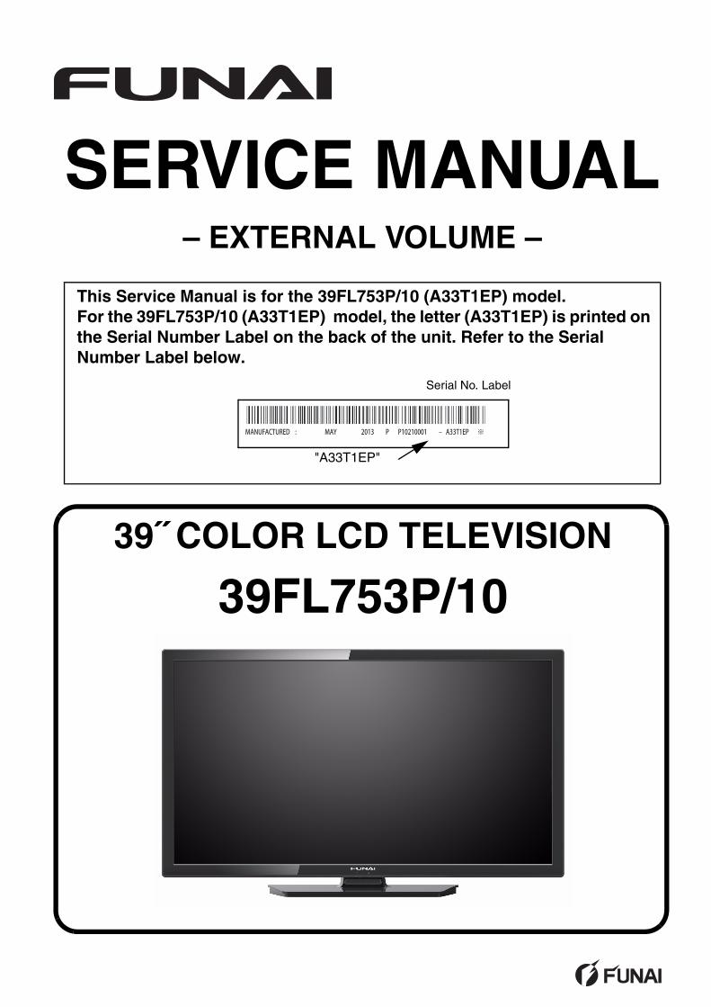
SERVICE MANUAL– EXTERNAL VOLUME –
This Service Manual is for the 39FL753P/10 (A33T1EP) model.For the 39FL753P/10 (A33T1EP) model, the letter (A33T1EP) is printed on the Serial Number Label on the back of the unit. Refer to the Serial Number Label below.
Serial No. Label
MANUFACTURED : MAY 2013 P P10210001 ‒ A33T1EP ※
"A33T1EP"
39˝ COLOR LCD TELEVISION
39FL753P/10

39˝ COLOR LCD TELEVISION
39FL753P/10
TABLE OF CONTENTSSpecifications. . . . . . . . . . . . . . . . . . . . . . . . . . . . . . . . . . . . . . . . . . . . . . . . . . . . . . . . . . . . . . . . . . . . . . . . . . . 1-1Important Safety Precautions. . . . . . . . . . . . . . . . . . . . . . . . . . . . . . . . . . . . . . . . . . . . . . . . . . . . . . . . . . . . . . . 2-1Standard Notes for Servicing . . . . . . . . . . . . . . . . . . . . . . . . . . . . . . . . . . . . . . . . . . . . . . . . . . . . . . . . . . . . . . . 3-1Cabinet Disassembly Instructions . . . . . . . . . . . . . . . . . . . . . . . . . . . . . . . . . . . . . . . . . . . . . . . . . . . . . . . . . . . 4-1Electrical Adjustment Instructions . . . . . . . . . . . . . . . . . . . . . . . . . . . . . . . . . . . . . . . . . . . . . . . . . . . . . . . . . . . 5-1How to Initialize the LCD Television. . . . . . . . . . . . . . . . . . . . . . . . . . . . . . . . . . . . . . . . . . . . . . . . . . . . . . . . . . 6-1Firmware Renewal Mode . . . . . . . . . . . . . . . . . . . . . . . . . . . . . . . . . . . . . . . . . . . . . . . . . . . . . . . . . . . . . . . . . . 7-1 Troubleshooting . . . . . . . . . . . . . . . . . . . . . . . . . . . . . . . . . . . . . . . . . . . . . . . . . . . . . . . . . . . . . . . . . . . . . . . . . 8-1Block Diagrams . . . . . . . . . . . . . . . . . . . . . . . . . . . . . . . . . . . . . . . . . . . . . . . . . . . . . . . . . . . . . . . . . . . . . . . . . 9-1Schematic Diagrams / CBA and Test Points . . . . . . . . . . . . . . . . . . . . . . . . . . . . . . . . . . . . . . . . . . . . . . . . . . 10-1Wiring Diagram . . . . . . . . . . . . . . . . . . . . . . . . . . . . . . . . . . . . . . . . . . . . . . . . . . . . . . . . . . . . . . . . . . . . . . . . 11-1Exploded View . . . . . . . . . . . . . . . . . . . . . . . . . . . . . . . . . . . . . . . . . . . . . . . . . . . . . . . . . . . . . . . . . . . . . . . . . 12-1Mechanical Parts List . . . . . . . . . . . . . . . . . . . . . . . . . . . . . . . . . . . . . . . . . . . . . . . . . . . . . . . . . . . . . . . . . . . . 13-1Electrical Parts List. . . . . . . . . . . . . . . . . . . . . . . . . . . . . . . . . . . . . . . . . . . . . . . . . . . . . . . . . . . . . . . . . . . . . . 14-1
The LCD panel is manufactured to provide many years of useful life.Occasionally a few non active pixels may appear as a tiny spec of color.This is not to be considered a defect in the LCD screen.
1-1 A33F0_F1 SP
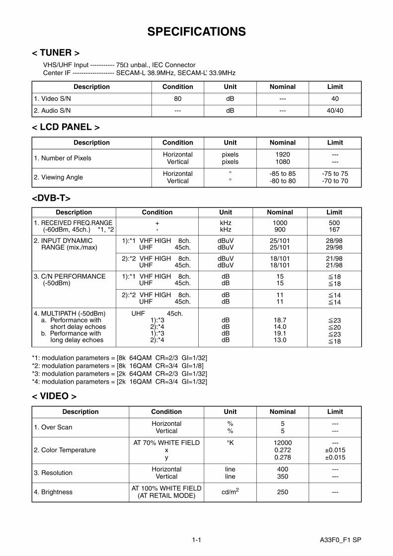
SPECIFICATIONS
< TUNER >VHS/UHF Input ----------- 75 unbal., IEC ConnectorCenter IF ------------------- SECAM-L 38.9MHz, SECAM-L’ 33.9MHz
< LCD PANEL >
<DVB-T>
*1: modulation parameters = [8k 64QAM CR=2/3 GI=1/32]*2: modulation parameters = [8k 16QAM CR=3/4 GI=1/8]*3: modulation parameters = [2k 64QAM CR=2/3 GI=1/32]*4: modulation parameters = [2k 16QAM CR=3/4 GI=1/32]
< VIDEO >
Description Condition Unit Nominal Limit
1. Video S/N 80 dB --- 40
2. Audio S/N --- dB --- 40/40
Description Condition Unit Nominal Limit
1. Number of Pixels HorizontalVertical
pixelspixels
19201080
------
2. Viewing Angle HorizontalVertical
°°
-85 to 85-80 to 80
-75 to 75-70 to 70
Description Condition Unit Nominal Limit
1. RECEIVED FREQ.RANGE (-60dBm, 45ch.) *1, *2
+-
kHzkHz
1000900
500167
2. INPUT DYNAMIC RANGE (mix./max)
1):*1 VHF HIGH 8ch.UHF 45ch.
dBuVdBuV
25/10125/101
28/9829/98
2):*2 VHF HIGH 8ch.UHF 45ch.
dBuVdBuV
18/10118/101
21/9821/98
3. C/N PERFORMANCE (-50dBm)
1):*1 VHF HIGH 8ch.UHF 45ch.
dBdB
1515
≦18≦18
2):*2 VHF HIGH 8ch.UHF 45ch.
dBdB
1111
≦14≦14
4. MULTIPATH (-50dBm) a. Performance with
short delay echoes b. Performance with
long delay echoes
UHF 45ch.1):*32):*41):*32):*4
dBdBdBdB
18.714.019.113.0
≦23≦20≦23≦18
Description Condition Unit Nominal Limit
1. Over Scan HorizontalVertical
%%
55
------
2. Color TemperatureAT 70% WHITE FIELD
xy
°K 120000.2720.278
---±0.015±0.015
3. Resolution HorizontalVertical
lineline
400350
------
4. Brightness AT 100% WHITE FIELD(AT RETAIL MODE) cd/m2 250 ---
1-2 A33F0_F1 SP
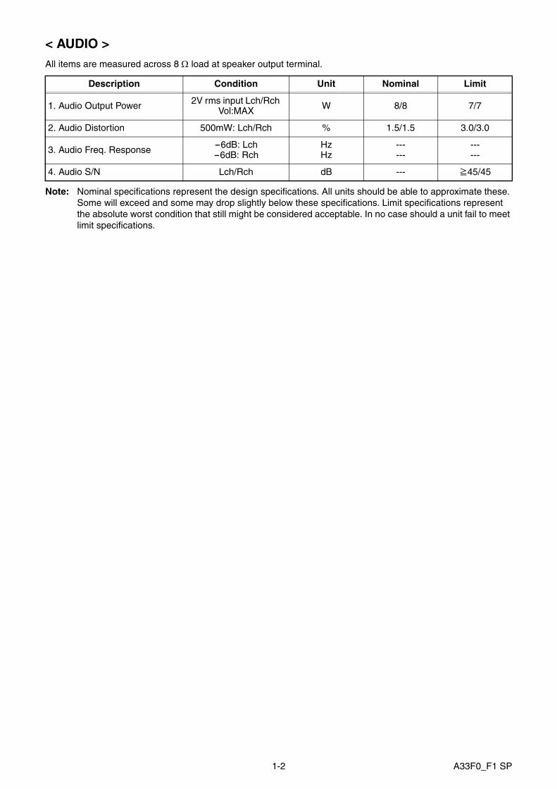
< AUDIO >All items are measured across 8 load at speaker output terminal.
Note: Nominal specifications represent the design specifications. All units should be able to approximate these. Some will exceed and some may drop slightly below these specifications. Limit specifications represent the absolute worst condition that still might be considered acceptable. In no case should a unit fail to meet limit specifications.
Description Condition Unit Nominal Limit
1. Audio Output Power 2V rms input Lch/Rch Vol:MAX W 8/8 7/7
2. Audio Distortion 500mW: Lch/Rch % 1.5/1.5 3.0/3.0
3. Audio Freq. Response -6dB: Lch-6dB: Rch
HzHz
------
------
4. Audio S/N Lch/Rch dB --- ≧45/45
2-1 LTVP_ISP
IMPORTANT SAFETY PRECAUTIONSPrior to shipment from the factory, our products are strictly inspected for recognized product safety and electrical codes of the countries in which they are to be sold. However, in order to maintain such compliance, it is equally important to implement the following precautions when a set is being serviced.
Safety Precautions for LCD TV Circuit1. Before returning an instrument to the
customer, always make a safety check of the entire instrument, including, but not limited to, the following items:
a. Be sure that no built-in protective devices are defective and have been defeated during servicing. (1) Protective shields are provided on this chassis to protect both the technician and the customer. Correctly replace all missing protective shields, including any removed for servicing convenience. (2) When reinstalling the chassis and/or other assembly in the cabinet, be sure to put back in place all protective devices, including but not limited to, nonmetallic control knobs, insulating fishpapers, adjustment and compartment covers/shields, and isolation resistor/capacitor networks. Do not operate this instrument or permit it to be operated without all protective devices correctly installed and functioning. Servicers who defeat safety features or fail to perform safety checks may be liable for any resulting damage.
b. Be sure that there are no cabinet openings through which an adult or child might be able to insert their fingers and contact a hazardous voltage. Such openings include, but are not limited to, (1) spacing between the LCD module and the cabinet mask, (2) excessively wide cabinet ventilation slots, and (3) an improperly fitted and/or incorrectly secured cabinet back cover.
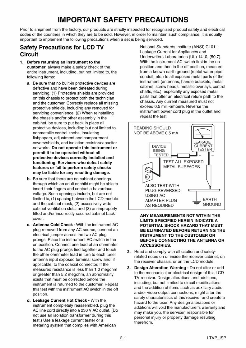
c. Antenna Cold Check - With the instrument AC plug removed from any AC source, connect an electrical jumper across the two AC plug prongs. Place the instrument AC switch in the on position. Connect one lead of an ohmmeter to the AC plug prongs tied together and touch the other ohmmeter lead in turn to each tuner antenna input exposed terminal screw and, if applicable, to the coaxial connector. If the measured resistance is less than 1.0 megohm or greater than 5.2 megohm, an abnormality exists that must be corrected before the instrument is returned to the customer. Repeat this test with the instrument AC switch in the off position.
d. Leakage Current Hot Check - With the instrument completely reassembled, plug the AC line cord directly into a 230 V AC outlet. (Do not use an isolation transformer during this test.) Use a leakage current tester or a metering system that complies with American
National Standards Institute (ANSI) C101.1 Leakage Current for Appliances and Underwriters Laboratories (UL) 1410, (50.7). With the instrument AC switch first in the on position and then in the off position, measure from a known earth ground (metal water pipe, conduit, etc.) to all exposed metal parts of the instrument (antennas, handle brackets, metal cabinet, screw heads, metallic overlays, control shafts, etc.), especially any exposed metal parts that offer an electrical return path to the chassis. Any current measured must not exceed 0.5 milli-ampere. Reverse the instrument power cord plug in the outlet and repeat the test.
ANY MEASUREMENTS NOT WITHIN THE LIMITS SPECIFIED HEREIN INDICATE A POTENTIAL SHOCK HAZARD THAT MUST BE ELIMINATED BEFORE RETURNING THE INSTRUMENT TO THE CUSTOMER OR BEFORE CONNECTING THE ANTENNA OR ACCESSORIES.
2. Read and comply with all caution and safety-related notes on or inside the receiver cabinet, on the receiver chassis, or on the LCD module.
3. Design Alteration Warning - Do not alter or add to the mechanical or electrical design of this LCD TV receiver. Design alterations and additions, including, but not limited to circuit modifications and the addition of items such as auxiliary audio and/or video output connections, might alter the safety characteristics of this receiver and create a hazard to the user. Any design alterations or additions will void the manufacturer's warranty and may make you, the servicer, responsible for personal injury or property damage resulting therefrom.
ALSO TEST WITHPLUG REVERSEDUSING ACADAPTER PLUGAS REQUIRED
TEST ALL EXPOSEDMETAL SURFACES
READING SHOULD NOT BE ABOVE 0.5 mA
EARTHGROUND
_
DEVICELEAKAGECURRENT
TESTER
+BEINGTESTED
2-2 LTVP_ISP
4. Hot Chassis Warning -
a. Some TV receiver chassis are electrically connected directly to one conductor of the AC power cord and maybe safety-serviced without an isolation transformer only if the AC power plug is inserted so that the chassis is connected to the ground side of the AC power source. To confirm that the AC power plug is inserted correctly, with an AC voltmeter, measure between the chassis and a known earth ground. If a voltage reading in excess of 1.0 V is obtained, remove and reinsert the AC power plug in the opposite polarity and again measure the voltage potential between the chassis and a known earth ground.
b. Some TV receiver chassis normally have 85V AC(RMS) between chassis and earth ground regardless of the AC plug polarity. This chassis can be safety-serviced only with an isolation transformer inserted in the power line between the receiver and the AC power source, for both personnel and test equipment protection.
c. Some TV receiver chassis have a secondary ground system in addition to the main chassis ground. This secondary ground system is not isolated from the AC power line. The two ground systems are electrically separated by insulation material that must not be defeated or altered.
5. Observe original lead dress. Take extra care to assure correct lead dress in the following areas: a. near sharp edges, b. near thermally hot parts-be sure that leads and components do not touch thermally hot parts, c. the AC supply, d. high voltage, and, e. antenna wiring. Always inspect in all areas for pinched, out of place, or frayed wiring. Check AC power cord for damage.
6. Components, parts, and/or wiring that appear to have overheated or are otherwise damaged should be replaced with components, parts, or wiring that meet original specifications. Additionally, determine the cause of overheating and/or damage and, if necessary, take corrective action to remove any potential safety hazard.
7. Product Safety Notice - Some electrical and mechanical parts have special safety-related characteristics which are often not evident from visual inspection, nor can the protection they give necessarily be obtained by replacing them with components rated for higher voltage, wattage, etc.. Parts that have special safety characteristics are identified by a ! on schematics and in parts lists. Use of a substitute replacement that does not have the same safety characteristics as the recommended replacement part might create shock, fire, and/or other hazards. The product's safety is under review continuously and new instructions are issued whenever appropriate. Prior to shipment from the factory, our products are strictly inspected to confirm they comply with the recognized product safety and electrical codes of the countries in which they are to be sold. However, in order to maintain such compliance, it is equally important to implement the following precautions when a set is being serviced.

2-3 LTVP_ISP
Precautions during ServicingA. Parts identified by the ! symbol are critical for
safety.Replace only with part number specified.
B. In addition to safety, other parts and assemblies are specified for conformance with regulations applying to spurious radiation. These must also be replaced only with specified replacements.Examples: RF converters, RF cables, noise blocking capacitors, and noise blocking filters, etc.
C. Use specified internal wiring. Note especially:
1) Wires covered with PVC tubing
2) Double insulated wires
3) High voltage leads
D. Use specified insulating materials for hazardous live parts. Note especially:
1) Insulation Tape
2) PVC tubing
3) Spacers
4) Insulators for transistors.
E. When replacing AC primary side components (transformers, power cord, etc.), wrap ends of wires securely about the terminals before soldering.
F. Observe that the wires do not contact heat producing parts (heat sinks, oxide metal film resistors, fusible resistors, etc.)
G. Check that replaced wires do not contact sharp edged or pointed parts.
H. When a power cord has been replaced, check that 5~6 kg of force in any direction will not loosen it.
I. Also check areas surrounding repaired locations.
J. Use care that foreign objects (screws, solder droplets, etc.) do not remain inside the set.
K. When connecting or disconnecting the internal connectors, first, disconnect the AC plug from the AC supply outlet.
L. When installing parts or assembling the cabinet parts, be sure to use the proper screws and tighten certainly.
2-4 LTVP_ISP
Safety Check after ServicingExamine the area surrounding the repaired locationfor damage or deterioration. Observe that screws,parts and wires have been returned to original posi-tions. Afterwards, perform the following tests and con-firm the specified values in order to verify compliancewith safety standards.
1. Clearance DistanceWhen replacing primary circuit components, confirmspecified clearance distance (d) and (d') between sol-dered terminals, and between terminals and surround-ing metallic parts. (See Fig. 1)
Table 1 : Ratings for selected area
Note: This table is unofficial and for reference only.Be sure to confirm the precise values.
2. Leakage Current TestConfirm the specified (or lower) leakage current be-tween B (earth ground, power cord plug prongs) andexternally exposed accessible parts (RF terminals, an-tenna terminals, video and audio input and output ter-minals, microphone jacks, earphone jacks, etc.).
Measuring Method : (Power ON)
Insert load Z between B (earth ground, power cordplug prongs) and exposed accessible parts. Use anAC voltmeter to measure across both terminals of loadZ. See Fig. 2 and following table.
Table 2: Leakage current ratings for selected areas
Note: This table is unofficial and for reference only. Be sure to confirm the precise values.
AC Line Voltage Clearance Distance (d), (d’)
220 to 240 V3mm(d)8mm(d’)
Fig. 1
Chassis or Secondary Conductor
Primary Circuit
d' d
Fig. 2
AC Voltmeter(High Impedance)
Exposed Accessible Part
B One side of Power Cord Plug Prongs
Z
AC Line Voltage Load Z Leakage Current (i) One side of power cord plug prongs (B) to:
220 to 240 V
2kRES. Connected in
parallel
i0.7mA AC Peaki2mA DC
RF orAntenna terminals
50k RES. Connected in
parallel
i0.7mA AC Peaki2mA DC A/V Input, Output
3-1 TVP_SN
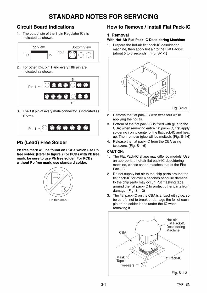
STANDARD NOTES FOR SERVICING
Circuit Board Indications1. The output pin of the 3 pin Regulator ICs is
indicated as shown.
2. For other ICs, pin 1 and every fifth pin are indicated as shown.
3. The 1st pin of every male connector is indicated as shown.
Pb (Lead) Free SolderPb free mark will be found on PCBs which use Pb free solder. (Refer to figure.) For PCBs with Pb free mark, be sure to use Pb free solder. For PCBs without Pb free mark, use standard solder.
How to Remove / Install Flat Pack-IC
1. RemovalWith Hot-Air Flat Pack-IC Desoldering Machine:
1. Prepare the hot-air flat pack-IC desoldering machine, then apply hot air to the Flat Pack-IC (about 5 to 6 seconds). (Fig. S-1-1)
2. Remove the flat pack-IC with tweezers while applying the hot air.
3. Bottom of the flat pack-IC is fixed with glue to the CBA; when removing entire flat pack-IC, first apply soldering iron to center of the flat pack-IC and heat up. Then remove (glue will be melted). (Fig. S-1-6)
4. Release the flat pack-IC from the CBA using tweezers. (Fig. S-1-6)
CAUTION:1. The Flat Pack-IC shape may differ by models. Use
an appropriate hot-air flat pack-IC desoldering machine, whose shape matches that of the Flat Pack-IC.
2. Do not supply hot air to the chip parts around the flat pack-IC for over 6 seconds because damage to the chip parts may occur. Put masking tape around the flat pack-IC to protect other parts from damage. (Fig. S-1-2)
3. The flat pack-IC on the CBA is affixed with glue, so be careful not to break or damage the foil of each pin or the solder lands under the IC when removing it.
Top View
Out In
Bottom ViewInput
5
10
Pin 1
Pin 1
Pb free mark
Fig. S-1-1
Hot-airFlat Pack-ICDesolderingMachine
CBA
Flat Pack-IC
Tweezers
Masking Tape
Fig. S-1-2
3-2 TVP_SN
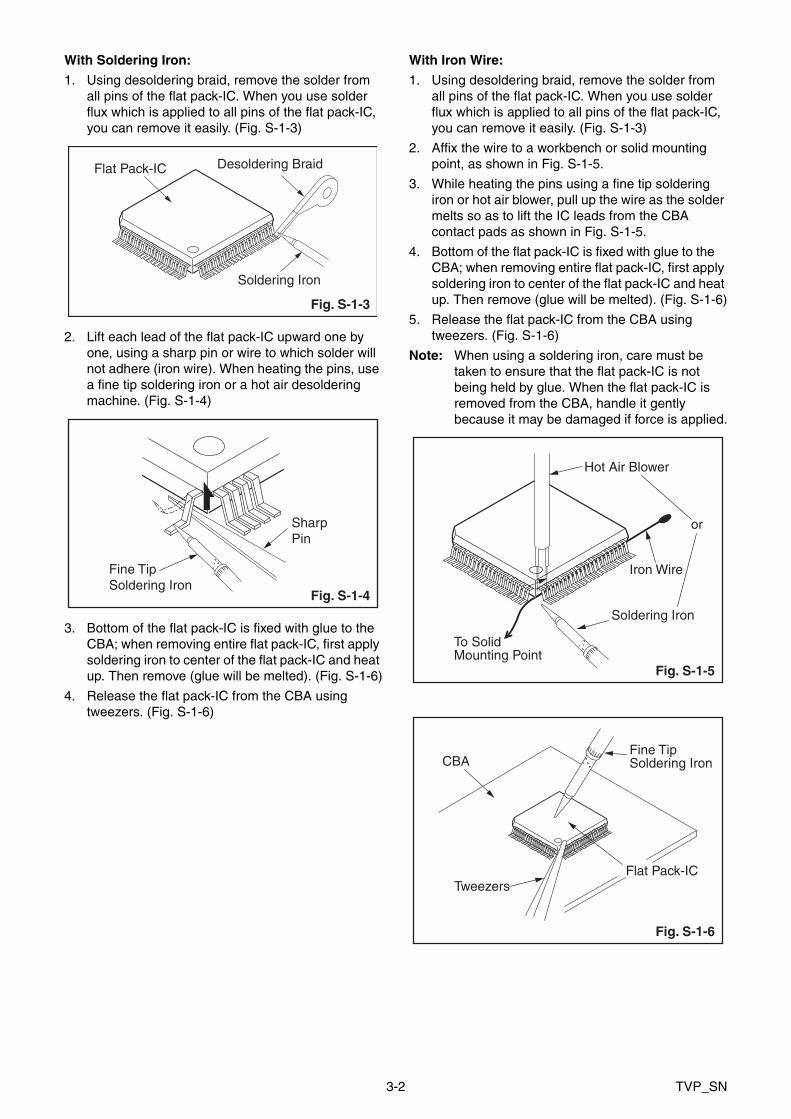
With Soldering Iron:
1. Using desoldering braid, remove the solder from all pins of the flat pack-IC. When you use solder flux which is applied to all pins of the flat pack-IC, you can remove it easily. (Fig. S-1-3)
2. Lift each lead of the flat pack-IC upward one by one, using a sharp pin or wire to which solder will not adhere (iron wire). When heating the pins, use a fine tip soldering iron or a hot air desoldering machine. (Fig. S-1-4)
3. Bottom of the flat pack-IC is fixed with glue to the CBA; when removing entire flat pack-IC, first apply soldering iron to center of the flat pack-IC and heat up. Then remove (glue will be melted). (Fig. S-1-6)
4. Release the flat pack-IC from the CBA using tweezers. (Fig. S-1-6)
With Iron Wire:
1. Using desoldering braid, remove the solder from all pins of the flat pack-IC. When you use solder flux which is applied to all pins of the flat pack-IC, you can remove it easily. (Fig. S-1-3)
2. Affix the wire to a workbench or solid mounting point, as shown in Fig. S-1-5.
3. While heating the pins using a fine tip soldering iron or hot air blower, pull up the wire as the solder melts so as to lift the IC leads from the CBA contact pads as shown in Fig. S-1-5.
4. Bottom of the flat pack-IC is fixed with glue to the CBA; when removing entire flat pack-IC, first apply soldering iron to center of the flat pack-IC and heat up. Then remove (glue will be melted). (Fig. S-1-6)
5. Release the flat pack-IC from the CBA using tweezers. (Fig. S-1-6)
Note: When using a soldering iron, care must be taken to ensure that the flat pack-IC is not being held by glue. When the flat pack-IC is removed from the CBA, handle it gently because it may be damaged if force is applied.
Flat Pack-IC Desoldering Braid
Soldering Iron
Fig. S-1-3
Fine TipSoldering Iron
SharpPin
Fig. S-1-4
To Solid Mounting Point
Soldering Iron
Iron Wire
or
Hot Air Blower
Fig. S-1-5
Fine TipSoldering IronCBA
Flat Pack-ICTweezers
Fig. S-1-6
3-3 TVP_SN
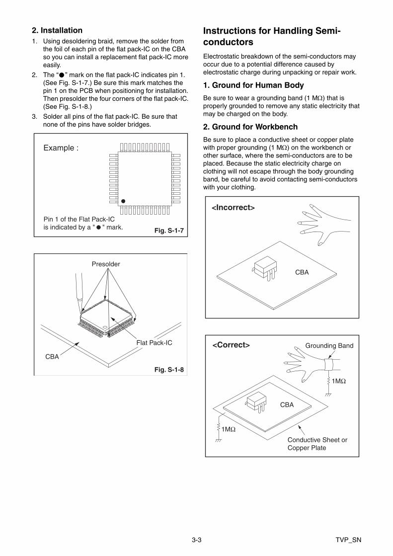
2. Installation1. Using desoldering braid, remove the solder from
the foil of each pin of the flat pack-IC on the CBA so you can install a replacement flat pack-IC more easily.
2. The “ I ” mark on the flat pack-IC indicates pin 1. (See Fig. S-1-7.) Be sure this mark matches the pin 1 on the PCB when positioning for installation. Then presolder the four corners of the flat pack-IC. (See Fig. S-1-8.)
3. Solder all pins of the flat pack-IC. Be sure that none of the pins have solder bridges.
Instructions for Handling Semi-conductorsElectrostatic breakdown of the semi-conductors may occur due to a potential difference caused by electrostatic charge during unpacking or repair work.
1. Ground for Human Body
Be sure to wear a grounding band (1 M) that is properly grounded to remove any static electricity that may be charged on the body.
2. Ground for Workbench
Be sure to place a conductive sheet or copper plate with proper grounding (1 M) on the workbench or other surface, where the semi-conductors are to be placed. Because the static electricity charge on clothing will not escape through the body grounding band, be careful to avoid contacting semi-conductors with your clothing.
Example :
Pin 1 of the Flat Pack-ICis indicated by a " " mark. Fig. S-1-7
Presolder
CBA
Flat Pack-IC
Fig. S-1-8
<Incorrect>
CBA
Grounding Band
Conductive Sheet orCopper Plate
1MΩ
1MΩ
<Correct>
CBA

4-1 A33T1 DC
CABINET DISASSEMBLY INSTRUCTIONS
1. Disassembly FlowchartThis flowchart indicates the disassembly steps for the cabinet parts and the CBA in order to gain access to items to be serviced. When reassembling, follow the steps in reverse order. Bend, route and dress the cables as they were.
2. Disassembly Method
Note:
(1) Order of steps in procedure. When reassembling, follow the steps in reverse order. These numbers are also used as the Identification (location) No. of parts in figures.
(2) Parts to be removed or installed.
(3) Fig. No. showing procedure of part location
(4) Identification of parts to be removed, unhooked, unlocked, released, unplugged, unclamped, or desoldered. P = Spring, L = Locking Tab, S = Screw, H = Hex Screw, CN = Connectore.g. 2(S-2) = two Screws of (S-2), 2(L-2) = two Locking Tabs of (L-2)
(5) Refer to the following "Reference Notes in the Table."
Important precautions concerning the LCD Panel Assembly:1. When you disassemble/re-assemble the X-PCB
Cover• Be careful not to break the hooks. If you pull with too
much force, the hooks may be damaged.• When disassembling, first hold the top and bottom of
the X-PCB Cover on both ends and then moving toward the center, lift up the top side to detach the hooks.
• When assembling, be careful not to damage the X-PCB Board or the COF(Chip On Film).
• Make sure the hooks are securely in place whenre-assembling.
• The screw tightening torque must be 5.2lb·in (6kgf·cm).
2. When you disassemble/re-assemble the Front Cabinet or Function CBA Unit
• Be careful not to break the hooks. If you pull with too much force, the hooks may be damaged.
• When disassembling, first detach the hooks on each end on the bottom side, then detach the remaining hooks moving toward the center.
• Make sure the hooks are securely in place when assembling.
• Be careful not to scratch the display panel when assembling.
• The Function CBA Unit and Sensor Lens are fixed in place by the hooks. Make sure these hooks are not damaged. Make sure the Function CBA Unit and Sensor Lens are securely in place when re-assembling.
• The screw tightening torque must be 5.2lb·in (6kgf·cm).
• After replacing the Front Cabinet or Function CBA Unit, make sure the tact switches operate normally.
• Make sure to replace the Control Plate to a new one when replacing the Front Cabinet.
Step/Loc. No.
Part Fig. No. Removal Note
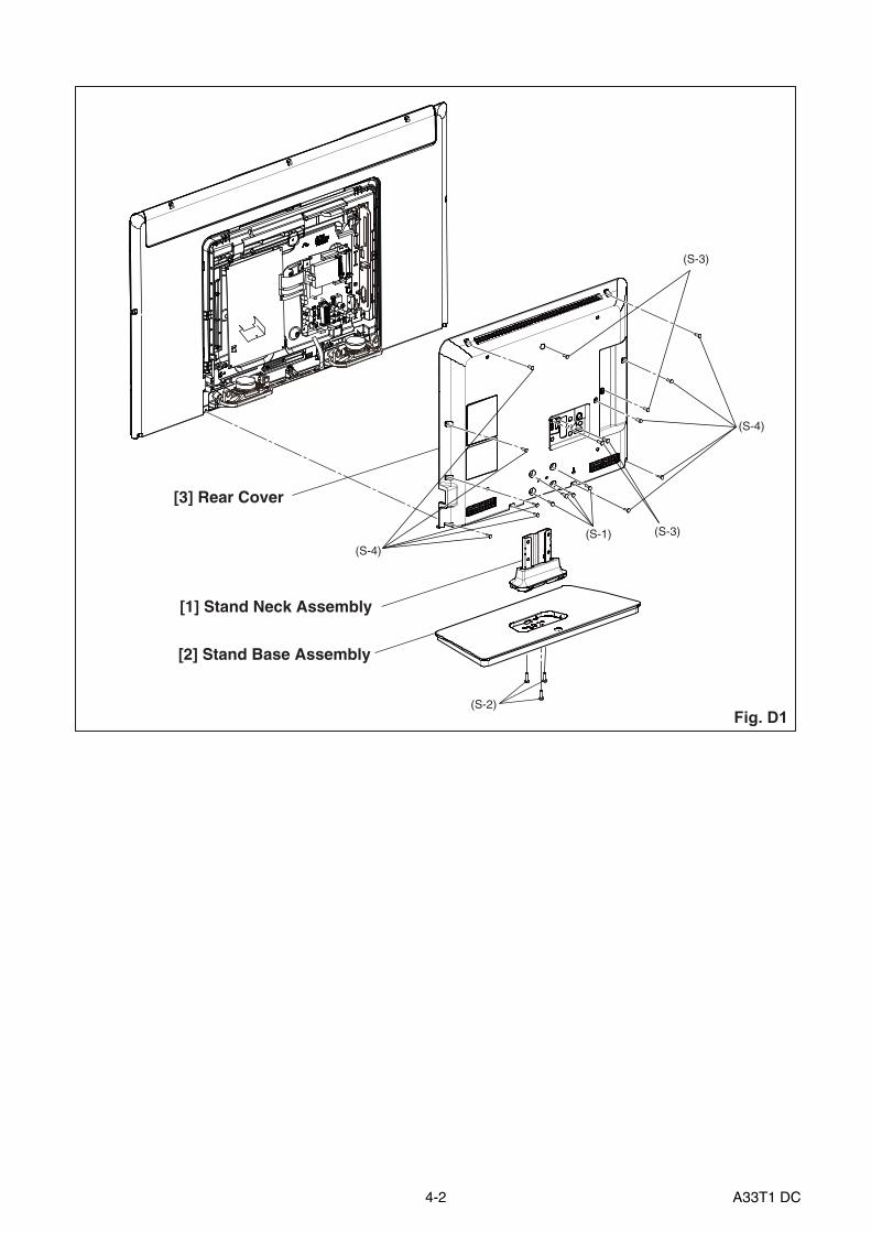
[1] Stand Neck Assembly D1 4(S-1), 3(S-2) ---
[2] Stand Base Assembly D1 --------------- ---
[3] Rear Cover D1 4(S-3), 10(S-4) ---
[4]Power Supply CBA
D2D5
5(S-5), CN101, CN102, CN103, CN104, CN105
---
[5] Digital Main CBA Unit
D2D5
4(S-6), CN7, CN12, CN18, Jack Holder ---
[6] Stand Bracket D3 2(S-7) ---
[7] Speaker D3 --------------- ---
[8] LCD Panel Assembly D3 --------------- ---
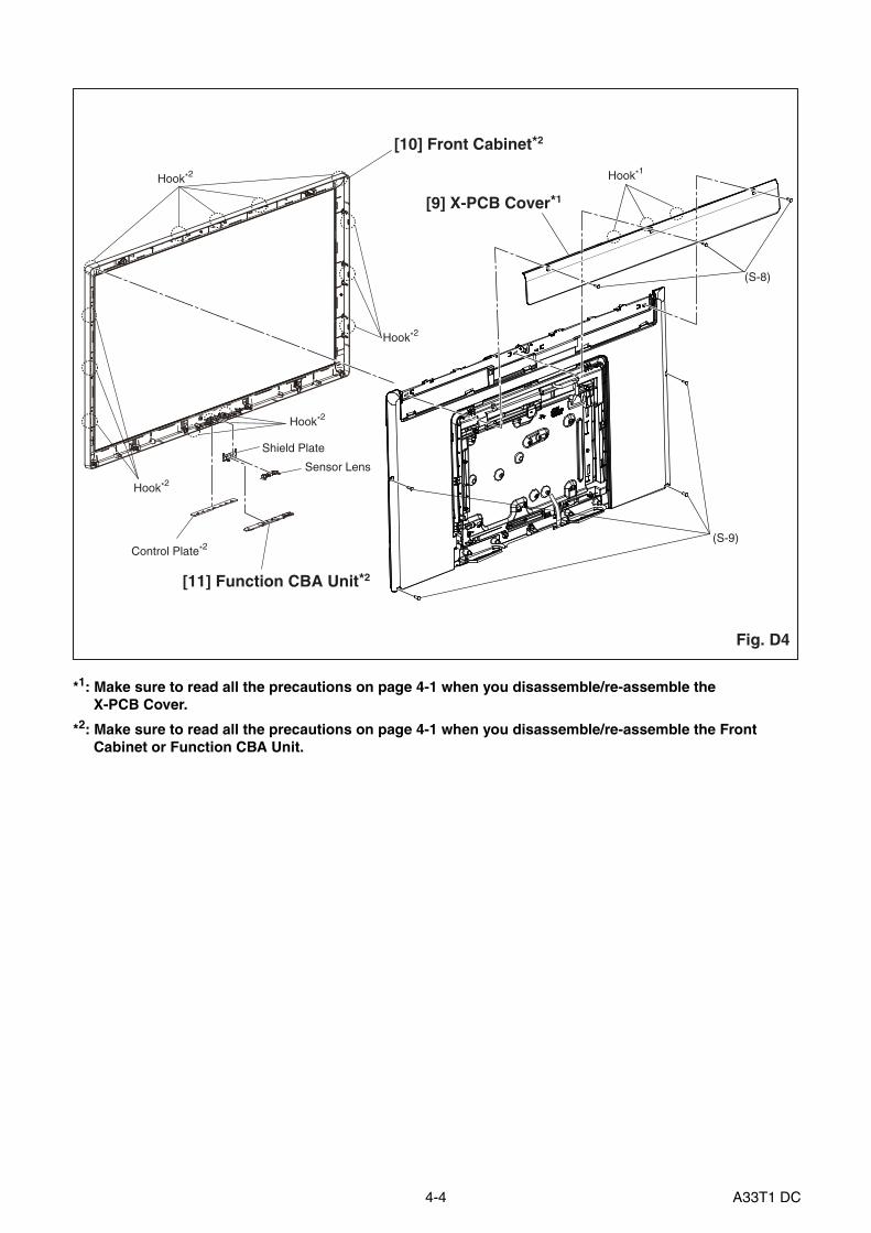
[9] X-PCB Cover D4 3(S-8) 1
[10] Front Cabinet D4 4(S-9) 2
[11] Function CBA Unit D4 Sensor Lens, Shield
Plate, Control Plate 2
(1)
(2)
(3)
(4)
(5)
[2] Stand Base Assembly
[3] Rear Cover[4] Power Supply CBA
[6] Stand Bracket
[7] Speaker
[5] Digital Main CBA Unit
[8] LCD Panel Assembly [9] X-PCB Cover
[1] Stand Neck Assembly
[10] Front Cabinet
[11] Function CBA Unit
4-2 A33T1 DC
(S-2)
[2] Stand Base Assembly
(S-3)
(S-4)
(S-3)
[1] Stand Neck Assembly
(S-4)(S-1)
[3] Rear Cover
Fig. D1

4-3 A33T1 DC
[4] Power Supply CBA
[5] Digital Main CBA Unit
(S-6)
(S-5)
Jack Holder
Fig. D2
[7] Speaker
[8] LCD Panel Assembly
[6] Stand Bracket
(S-7)
Fig. D3
4-4 A33T1 DC
[11] Function CBA Unit*2
(S-9)
Sensor Lens
Control Plate*2
[10] Front Cabinet*2
Shield Plate
Hook*2
Hook*2
Hook*2
Hook*2
[9] X-PCB Cover*1
(S-8)
Hook*1
Fig. D4
*1: Make sure to read all the precautions on page 4-1 when you disassemble/re-assemble theX-PCB Cover.
*2: Make sure to read all the precautions on page 4-1 when you disassemble/re-assemble the Front Cabinet or Function CBA Unit.
4-5 A33T1 DC
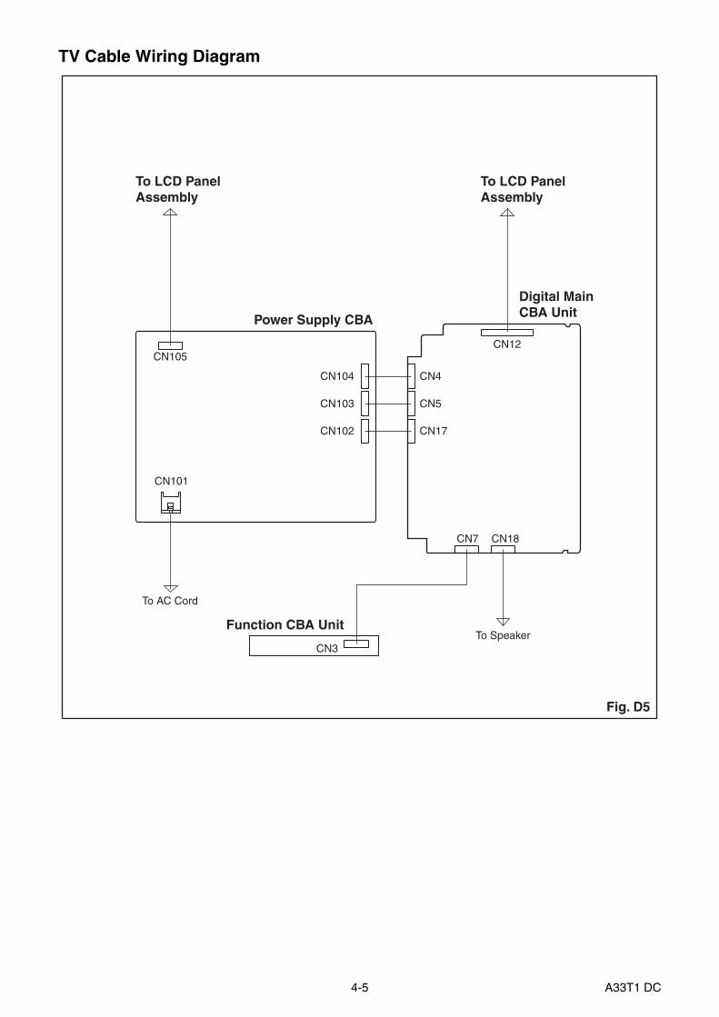
TV Cable Wiring Diagram
Power Supply CBA
Function CBA Unit
To LCD Panel Assembly
To LCD Panel Assembly
To AC Cord
To Speaker
Digital MainCBA Unit
CN7 CN18
CN12
CN3
CN105
CN101
CN104
CN103
CN102
CN4
CN5
CN17
Fig. D5
5-1 LC11P(A33M1_M0EP)EA
ELECTRICAL ADJUSTMENT INSTRUCTIONS
General Note: “CBA” is abbreviation for “Circuit Board Assembly.”Note: Electrical adjustments are required after
replacing circuit components and certain mechanical parts. It is important to perform these adjustments only after all repairs and replacements have been completed. Also, do not attempt these adjustments unless the proper equipment is available.
Test Equipment Required1. Remote control unit
2. Color Analyzer, CA-310 (KONICA MINOLTA Luminance meter) or measuring instrument as good as CA-310.
How to set up the service mode:
Service mode:1. Turn the power on.
2. Press [SOURCE], [2], [5], [8] and [0] buttons on the remote control unit in this order to enter the service mode. The Factory Setting menu appears in the screen.
Example:
0123456789
101112
White BalanceAging ModePictureSoundGeneralDebugEMCSystem InfoUpgradeInit fac channel tblInit TVADC AdjustFactory Reset
>>>>>>->->->->->->->
>>>>>>->
>>>
T.MSD309.B95X0xAE1E
2013-01-30 16:02:15
Main boardChecksumBuild Time
Factory Settings
5-2 LC11P(A33M1_M0EP)EA
The White Balance Adjustment should be performed when replacing the LCD Panel or Digital Main CBA.
1. White Balance AdjustmentPurpose: To mix red and blue beams correctly for pure white.
Symptom of Misadjustment: White becomes bluish or reddish.
1. Operate the unit for more than 60 minutes.
2. Input the White Raster of composite video signal to AV (70%=70IRE, 40%=40IRE).
3. Enter the service mode.
4. Press [0] button on the remote control unit to display the “White Balance” menu.
Additional step: A1. Press [2] button on the remote control unit to select the “Colour Temp” menu. A2. Press [s] or [B] button to select the "Normal".
5. Select a color mode (“3 R-GAIN”, “5 B-GAIN”, “6 R-OFFSET” or “8 B-OFFSET”).
6. Set the color analyzer at the CHROMA mode and zero point calibration. Bring the optical receptor pointing at the center of the LCD-Panel.
Note: The optical receptor must be set perpendicularly to the LCD Panel surface.
7. In each color mode, press [s] or [B] button to adjust the color temperature becomes 12000°K (x= 0.272 / y= 0.278 ±0.015).
8. To cancel or to exit from the White Balance Adjustment, press [BACK] button.
INPUT SIGNAL
Color Analyzer
Perpendicularity
To avoid interference from ambient light, this adjustment should be performed in a dark room.
INPUT: WHITE 70%, 40%
L = 1 cm
6-1 LC11P_INT
HOW TO INITIALIZE THE LCD TELEVISION
1. Turn the power on.
2. Enter the service mode. (Refer to page 5-1.)
- To cancel the service mode, press [BACK] button on the remote control unit.
3. Select “Factory Reset” and [OK] button on the remote control unit.The TV set will go off and turn back on automatically when initialization completes.

7-1 LC11P_FW
FIRMWARE RENEWAL MODE
Equipment Requireda. USB storage deviceb. Remote Control Unit
Firmware Update Procedure
[Preparation]1. Prepare USB storage device.
2. Copy F/W-file to USB storage device.Note: Make sure to use the blank USB Storage.
3. Make sure that the F/W-file’s name is “LC11_308B_FUNAI.bin”.
[Update procedure]1. Turn the power on.
2. Insert USB storage device with F/W to TV set.
3. Press the [MENU] button on the remote control unit to display Menu.
4. Select “SETUP”.
5. Select “Software Update (USB)” and press [OK] button. The message “Are you sure?” will appear in the screen.
6. Press [LEFT] button to select “YES”.
7. Updating starts.
Note: Do not turn off the TV set and do not remove the USB storage device while this procedure.
8. The TV set will go off and turn back on automatically when update completes.
Additional step: A1. Enter the service mode. A2. Select "Init TV" and press [OK] button. The TV set will go off and go back on automaticaly. A3. Adjust the white balance.
[Confirmation of update]1. Enter the service mode. (Refer to page 5-1.)
2. Check the “Checksum” section.

8-1 A33T1TR
TROUBLESHOOTING
[Power Supply Section]
When buzz sound can be heard in the periphery of power circuit.FLOW CHART NO.4
Check if there is any short-circuit on the rectifying diode and the circuit in each rectifying circuit of the secondary side. Repair it if defective. (D401, D402, D403, D501, D502, D503, D509, D510, IC501, Q403, Q701)
The power cannot be turned on.
The fuse blows out.
FLOW CHART NO.1
FLOW CHART NO.2
Is normal state restored when once unpluggedpower cord is plugged again after several seconds?
Check if there is any leak or short-circuit on theprimary circuit component and repair it if defective.(C608, D601, D602, D603, D604, D605, D608, D609, D612, D615, D618, D622, D623, IC601, IC602, Q601, Q602, Q603, R603, R604, T601)
Yes
No
Yes
Is the fuse (F602) normal? See FLOW CHART No.2 <The fuse blows out.>
No
Yes
Is the P-ON+21V line voltage normal?No
Check each rectifying circuit of the secondarycircuit and repair it if defective.
Check if there is any leak or short-circuit on theprimary circuit component and repair it if defective.
Check if there is any leak or short-circuit on theeach rectifying circuit component of secondary side and repair it if defective.
Make sure to repair the primary circuit component before replacing the fuse (F602).
When the output voltage fluctuates.FLOW CHART NO.3
Does the photocoupler circuit on the secondary side operate normally?
No
Yes
Check D504, IC301, IC601 and their periphery circuit. Repair it if defective.
Check D608, D609, D612, D618, D622, D623, IC601, IC602, Q601, Q602, Q603 and their periphery circuit. Repair it if defective.

8-2 A33T1TR
No
AMP+13V is not output.FLOW CHART NO.6
Is approximately +14V voltage supplied to the cathode of D401(D402, D403)?
Yes
Check C402, C403, C407, C408, D401, D402, D403 and their periphery circuit. Repair it if defective.
Check C402, C403, C407, C408, D401, D402, D403 and their periphery circuit. Repair it if defective.
Check C402, C403, C407, C408, D401, D402, D403 and their periphery circuit. Repair it if defective.
Check IC701, Q702, Q703, PS-ON line and their periphery circuit. Repair it if defective.
Check D507 and their periphery circuit. Repair it if defective.
Check if there is any leak or short-circuit on the loadcircuit. Repair it if defective.
Check if there is any leak or short-circuit on the loadcircuit. Repair it if defective.
P-ON+21V is not output.FLOW CHART NO.5
Is approximately +21V voltage supplied to the cathode of D501(D502, D503, D509, D510)?
No
Yes
Check C502, C503, C504, C513, D501, D502, D503, D504, D509, D510 and their periphery circuit. Repair it if defective.
Check C502, C503, C504, C513, D501, D502, D503, D504, D509, D510 and their periphery circuit. Repair it if defective.
PANEL+5V(+5V) is not output.FLOW CHART NO.8
Is approximately +21V voltage supplied to Pin(8) of IC501?
Is approximately +2V voltage supplied to Pin(7) of IC501?
NoYes
Yes
No
Replace IC501.
Check IC402, R404, R407, R409 and their periphery circuit. Repair it if defective.
STB+5V is not output.FLOW CHART NO.9
Is approximately +11V voltage supplied to the drain of Q403?
Is approximately +8V voltage supplied to the gate of Q403?
NoYes
Yes
No
Replace Q403.
P-ON+13V is not output.FLOW CHART NO.7
Is approximately +14V voltage supplied to the drain of Q701?
Is approximately +16V voltage supplied to the gate of Q701?
NoYes
Yes
No
Replace Q701.

8-3 A33T1TR
[Video Signal Section]
NoIs the "L" pulse supplied to Pin(4) of CN7 when the infrared remote control is activated?
Yes
Is approximately +5V voltage supplied to Pin(1) of CN7?
No
FLOW CHART NO.2
Check STB+5V line and repair it if defective.
Yes
Replace the Digital Main CBA Unit.
When pressing each buttons, does the Pin(6) voltage of CN7 decrease?
The key operation is not functioning.FLOW CHART NO.1
Yes
Replace the Digital Main CBA Unit.
Replace the Function CBA Unit.
Replace the Function CBA Unit or the remote control unit.
No
No operation is possible from the remote control unit. (Operation is possible from the unit.)
Picture does not appear normally.FLOW CHART NO.3
Is approximately +13V voltage supplied to Pin(1, 2) of CN103?
Digital Main CBA Unit or LCD Panel Assembly may be defective. Check and replace these parts.
No
Yes
Is approximately +5V voltage supplied to Pin(1) of CN104?
See FLOW CHART NO.9 <STB+5V is not output.[Power Supply Section]>
See FLOW CHART NO.7 <P-ON+13V is not output.[Power Supply Section]>
Is approximately +5V voltage supplied to Pin(5, 6, 7, 8) of CN104?
No
Yes
See FLOW CHART NO.8 <PANEL+5V(+5V) is not output. [Power Supply Section]>
No
Yes
8-4 A33T1TR
[Audio Signal Section]
SP3801, SP3802 or CL18 may be defective. Check and replace these parts.
Audio is not output normally.FLOW CHART NO.1
Are the audio signals output to Pin(1, 2, 3, 4) of CN18? Replace the Digital Main CBA Unit.No
Yes
Is approximately +14V voltage supplied to Pin(1, 2) of CN102?
No
Yes
See FLOW CHART NO.6 <AMP+13V is not output. [Power Supply Section]>
Yes
Is approximately +5V voltage supplied to Pin(1) of CN104?
See FLOW CHART NO.9 <STB+5V is not output.[Power Supply Section]>
Is approximately +5V voltage supplied to Pin(5, 6, 7, 8) of CN104?
No See FLOW CHART NO.8 <PANEL+5V(+5V) is not output. [Power Supply Section]>
No
Yes
9-1
TO L
ED
BA
CK
LIG
HT
DR
IVE
B
LOC
K D
IAG
RA
M
TO P
OW
ER
SU
PP
LY
BLO
CK
DIA
GR
AM
P
S-O
N
CN
4
CN
5
QE
22
QB
11
QE
21
QF
31
BA
CK
LIG
HT-
SW
B
AC
KLI
GH
T-A
DJ
FU
NC
TIO
N C
BA
UN
IT
PO
WE
R S
UP
PLY
CB
A
CN
104
CN
103
ST
B+
5V
M+
5V
ST
B+
3.3V
U1
(MA
IN M
ICR
O C
ON
TR
OLL
ER
)
DIG
ITA
L M
AIN
CB
A U
NIT
XTA
L-O
UT
X
TAL-
IN
Y1 24
MH
z O
SC
R
ES
ET
BL-
EN
LED
-R
PO
W-E
N
RE
MO
TE
PW
M1
PW
M2
UF
11 (
ME
MO
RY
)
SC
K
SI
SO
6 5 2 1
TU
NE
R-S
CL
TU
NE
R-S
DA
CS
#
PO
WE
R
SO
UR
CE
M
EN
U
CH
+
CH
-
VO
L+
VO
L-
KE
Y-S
W
SP
I-S
CK
S
PI-
SD
I S
PI-
SD
O
SP
I-C
SN
TO A
UD
IO
BLO
CK
DIA
GR
AM
A
MP
-MU
TE
A
MP
-MU
TE
SC
L S
DA
3 4
T1
(TU
NE
R U
NIT
)
D15
P
OW
ER
RE
1 R
EM
OT
E
SE
NS
OR
PS
-ON
2
2
CN
7 C
N3
RE
MO
TE
4
4
LED
-R
22
IR-K
EY
6
6
BA
CK
LIG
HT-
SW
3
3 4
4 B
AC
KLI
GH
T-A
DJ
RE
SE
T
QB
1
L20
B3
A3
B4
L6
Y4
AA
4
V17
V16
K6
H6
L5
W4
W5
J5
KE
YA
J1
4 T
8
QB
12
BLOCK DIAGRAMS
A33T1BLS
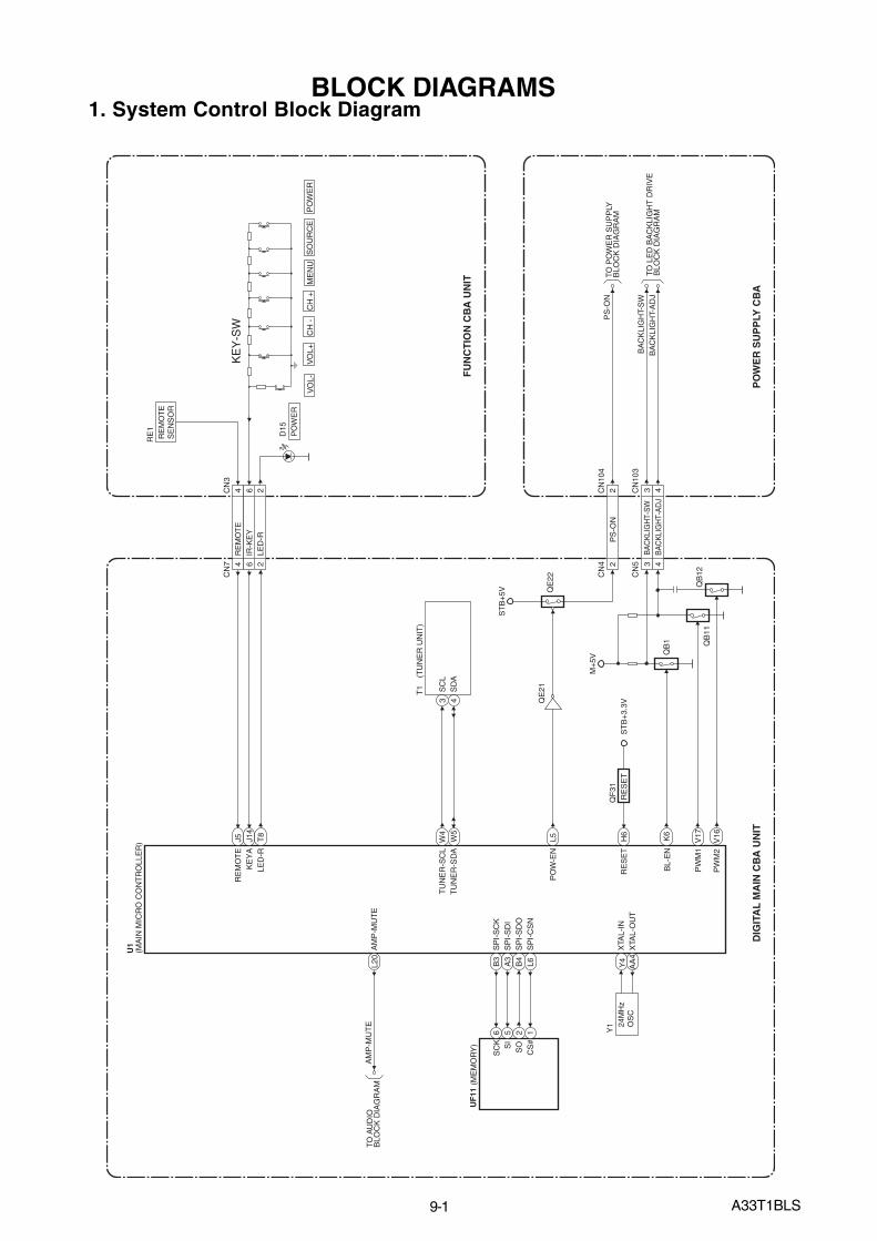
1. System Control Block Diagram

9-2 A33T1BLV
CO
MP
ON
EN
T-Y
INVID
EO
-IN
CO
MP
ON
EN
T-P
b-IN
CO
MP
ON
EN
T-P
r-IN
CN
8
QS
1, Q
S2
AV
11AV
8S
CA
RT
JA
CK
1520 11 7V
IDE
O-B
VID
EO
-G
VID
EO
-R
19
RG
B-V
IDE
O-I
N
RG
B-V
IDE
O-O
UT
VID
EO
SIG
NA
L
T1
IF_P
IF_N
IF_P
8IF
_N7
(TU
NE
R U
NIT
)
IF-A
GC
9
RG
B-V
IDE
O-I
N
RG
B-V
IDE
O-O
UT
VID
EO
-RV
IDE
O-G
VID
EO
-B
TO D
IGIT
AL
SIG
NA
LP
RO
CE
SS
BLO
CK
DIA
GR
AM
TO D
IGIT
AL
SIG
NA
LP
RO
CE
SS
BLO
CK
DIA
GR
AM
VID
EO
-IN
CO
M-Y
-IN
CO
M-P
b-IN
CO
M-P
r-IN
IF-A
GC
AU
DIO
SIG
NA
L
DIG
ITA
L M
AIN
CB
A U
NIT
BU
FF
ER
2. Video Block Diagram
9-3 A33T1BLA
AU
DIO
SIG
NA
L
PC
-AU
DIO
-IN
AU
DIO
(L)
AU
DIO
(R)
PC
-AU
DIO
(L)
PC
-AU
DIO
(R)
RG
B-A
UD
IO(L
)-O
UT
RG
B-A
UD
IO(R
)-O
UT
AM
P-M
UT
E
AU
DIO
(L)-
IN
DIG
ITA
LA
UD
IO-O
UT
(CO
AX
IAL)
AU
DIO
(R)-
IN
AV
27
AV
7
AV
11 13R
GB
-AU
DIO
(L)-
OU
T
RG
B-A
UD
IO(R
)-O
UT
6R
GB
-AU
DIO
(L)-
IN
RG
B-A
UD
IO(R
)-IN
TO D
IGIT
ALS
IGN
AL
PR
OC
ES
SB
LOC
K D
IAG
RA
M
TO S
YS
TE
MC
ON
TR
OL
BLO
CK
DIA
GR
AM
DIG
ITA
L M
AIN
CB
A U
NIT
CN
18
SP
EA
KE
RL-
CH
3
SP
EA
KE
RR
-CH
SP
(R)+
SP
(R)-
42S
P(L
)+
SP
(L)-
1
AV
30H
EA
DP
HO
NE
JAC
K
2
1,2
UA
31 (
AU
DIO
AM
P)
3
MU
TE
L+D
RIV
E
L-D
RIV
E
R-D
RIV
E
PW
M
12R
+D
RIV
EP
WM
17,1
8
20,2
1
22,2
3
25,2
6
QA
32
QA
31A
MP
+13
V
SP
DIF
RG
B-A
UD
IO(L
)-IN
RG
B-A
UD
IO(R
)-IN
AM
P(L
)-O
UT
AM
P(R
)-O
UT
AV
8S
CA
RT
JA
CK
QS
5, Q
S6
BU
FF
ER
QS
3, Q
S4
BU
FF
ER
SP
3801
SP
3802
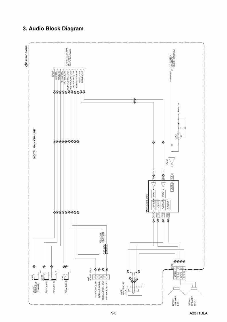
3. Audio Block Diagram

9-4 A33T1BLD
IF_P
IF
_N
DIG
ITA
L M
AIN
CB
A U
NIT
U1
(D
IGIT
AL
SIG
NA
L P
RO
CE
SS
)
LVD
S
TX
DIG
ITA
L
SIG
NA
L
PR
OC
ES
S
PC
-RG
B-I
N
3
12
15
1
2
RE
D
GR
EE
N
BL
UE
DATA
C
LO
CK
AV
6
A/D
C
ON
VE
RT
ER
14
13
HS
YN
C
VS
YN
C
VID
EO
-R
VID
EO
-G
VID
EO
-B
TO
VID
EO
B
LO
CK
D
IAG
RA
M
TO
VID
EO
B
LO
CK
D
IAG
RA
M
TO
VID
EO
B
LO
CK
DIA
GR
AM
TO
AU
DIO
B
LO
CK
D
IAG
RA
M
SW
RG
B-V
IDE
O-I
N
IF-A
GC
PC
-HS
P
C-V
S
VG
A-S
DA
V
GA
-SC
L
IF-A
GC
DE
MO
DU
LAT
OR
/M
PE
G D
EC
OD
ER
AU
DIO
I/F
CI
CO
NT
RO
L H
DM
I I/
F
MH
L/
HD
MI-
to-H
DM
I B
ridge
AU
DIO
DE
CO
DE
R
VID
EO
D
EC
OD
ER
VID
EO
SIG
NA
L
AU
DIO
SIG
NA
L
CI
CA
RD
S
LO
T
AV
20
DA
C
SP
DIF
LC
D P
AN
EL
A
SS
EM
BLY
18
1
9
20
2
1
22
2
3
17
1
6
15
29
3
0
37
3
8
39
4
0
28
2
7
24
12
1
1
CN
12
10
9
8
7
DQ
U(0
-7)
DQ
L (
0-7
)
A(0
-13
)
U2 (
SD
RA
M)
A-M
DQ
U(0
-7)
A-M
DQ
L (
0-7
)
MA
-A(0
-13
)
CI-
D(0
-7)
CI-
A(0
-14
)
CO
M-Y
-IN
V
IDE
O-I
N
CO
M-P
b-I
N
CO
M-P
r-IN
RG
B-V
IDE
O-O
UT
HD
MI-
IN1
A
V1
TM
DS
-D0
(+)
TM
DS
-D0
(-)
TM
DS
-D1
(+)
TM
DS
-D1
(-)
TM
DS
-D2
(+)
TM
DS
-D2
(-)
SD
A
SC
L
7
9
4
6
1
3
10
1
2
16
1
5
TM
DS
-CL
OC
K(+
) T
MD
S-C
LO
CK
(-)
HD
MI
SW
HD
MI-
IN3
A
V3
7
9
4
6
1
3
10
1
2
16
1
5
AU
DIO
(L)
AU
DIO
(R)
PC
-AU
DIO
(L)
PC
-AU
DIO
(R)
RG
B-A
UD
IO(L
)-O
UT
R
GB
-AU
DIO
(R)-
OU
T
RG
B-A
UD
IO(L
)-IN
R
GB
-AU
DIO
(R)-
IN
AM
P(L
)-O
UT
A
MP
(R)-
OU
T
DE
SC
RA
MB
LE
R
/TS
IN
TE
RFA
CE
R2
L1
L3
L
2
M1
K2
J2
J3
P3
N
3
M2
P
2
P1
U
7
V7
W2
W
1
V2
U4
U5
U1
U6
AA
2
Y2
T6
T7
Y3
AA
3
H15
T3
T2
R19
T1
9 T2
0 U
19
U20
W21
V1
9 Y2
1 W
20
Y20
W19
Y1
9 AA
20
W18
AA
19
V21
V20
Y18
AA18
U3
G3
F2
H3
G2
H1
H2
F1
F3
C5
D5
HD
MI-
IN2
A
V2
TM
DS
-D0
(+)
TM
DS
-D0
(-)
TM
DS
-D1
(+)
TM
DS
-D1
(-)
TM
DS
-D2
(+)
TM
DS
-D2
(-)
SD
A
SC
L
7
9
4
6
1
3
10
1
2
16
1
5
TM
DS
-CL
OC
K(+
) T
MD
S-C
LO
CK
(-)
D3
C
2
E3
E2
E1
E2
C1
C3
C4
D4
AA
6
Y6
AA
7
W6
W
7
Y7
AA
5
Y5
V8
U
8
R20
T21
R21
P19
P20
TM
DS
-D0
(+)
Sil1
292
U1
8
TM
DS
-D0
(-)
TM
DS
-D1
(+)
TM
DS
-D1
(-)
TM
DS
-D2
(+)
TM
DS
-D2
(-)
SD
A
SC
L
TM
DS
-CL
OC
K(+
) T
MD
S-C
LO
CK
(-)
35
3
4
37
3
6
39
3
8
33
3
2
7
8
25
2
4
27
2
6
29
2
8
23
2
2
17
1
8
RX
O0(
-)
RX
O0(
+)
RX
O1(
-)
RX
O1(
+)
RX
O2(
-)
RX
O2(
+)
RX
OC
(-)
RX
OC
(+)
RX
O3(
-)
RX
O3(
+)
RX
E0(
-)
RX
E0(
+)
RX
E1(
-)
RX
E1(
+)
RX
E2(
-)
RX
E2(
+)
RX
EC
(-)
RX
EC
(+)
RX
E3(
-)
RX
E3(
+)
RX
O4(
-)
RX
O4(
+)
RX
E4(
-)
RX
E4(
+)
MH
L_
SD
A
MH
L_
SC
L
I2C
_S
DA
I2
C_
SC
L
H20
H1
9
4. Digital Signal Process Block Diagram
9-5
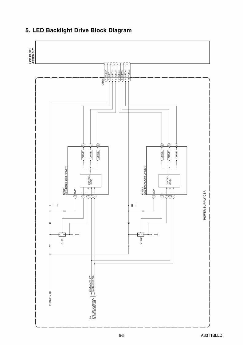
5. LED Backlight Drive Block Diagram
VLE
D1
1IL
ED
13
PO
WE
R S
UP
PLY
CB
A
LC
D P
AN
EL
AS
SE
MB
LY
ILE
D2
4IL
ED
35
ILE
D4
7IL
ED
58
ILE
D6
9V
LED
211
IC10
01
(LE
D B
AC
KLI
GH
T D
RIV
ER
)
OV
P
CN
105
DR
IVE
Q10
01
CO
NTR
OL
LOG
IC
10 16 14 13 1
DR
IVE
32
DR
IVE
5
P-O
N+
21V
BA
CK
LIG
HT-
AD
JB
AC
KLI
GH
T-S
WTO
S
YS
TE
M C
ON
TR
OL
BLO
CK
DIA
GR
AM
IC10
02(L
ED
BA
CK
LIG
HT
DR
IVE
R)
OV
P
DR
IVE
Q10
02
CO
NTR
OL
LOG
IC
10 16 14 13 1
DR
IVE
32
DR
IVE
5
A33T1BLLD
9-6
HO
T C
IRC
UIT
. BE
CA
RE
FU
L.
CN
101
W
B
AC
601
AC
CO
RD
L6
01
PO
WE
R S
UP
PLY
CB
A
F60
2 T
3.15
A H
/250
V
LIN
E
FIL
TE
R
L603
LIN
E
FIL
TE
R
BR
IDG
E
RE
CT
IFIE
R
D60
1-D
604
1 4 3
2
(FE
ED
BA
CK
) IC
601
Q60
1
Q60
2
T60
1
6 2 1 5 4
7 8 11
12
9 10
OU
T
VH
IS
FB
SW
ITC
HIN
G
SW
ITC
HIN
G
5 8 3 2
VC
C
6
IC60
2 (S
WIT
CH
ING
CO
NT
RO
L)
IC30
1 S
HU
NT
R
EG
.
SW
+5V
SW
+5V
Q70
3
SW
+13
V
SW
Q70
1
Q70
2
Q40
3
PS
-ON
TO
SY
ST
EM
CO
NT
RO
L
BLO
CK
DIA
GR
AM
CN
102
CN
103
CN
17
CN
5
1,2
AM
P+
13V
1,
2
1,2
P-O
N+
13V
1,
2
CN
104
C
N4
1 S
TB
+5V
1
5-8
+5V
5-
8
AM
P+
13V
P-O
N+
13V
D
LO
C
TO
H
DIG
ITA
L M
AIN
CB
A U
NIT
Q30
1
M+
5V
PA
NE
L+5V
P-O
N+
21V
ST
B+
5V
IC70
1
IC40
2 IC50
1
SH
UN
T
RE
G.
SH
UN
T
RE
G.
CA
UT
ION
!F
ixed
vol
tage
(or
Aut
o vo
ltage
sel
ecta
ble)
pow
er s
uppl
y ci
rcui
t is
used
in th
is u
nit.
If M
ain
Fus
e (F
602)
is b
low
n , c
heck
to s
ee th
at a
ll co
mpo
nent
s in
the
pow
er s
uppl
y ci
rcui
t are
not
def
ectiv
e be
fore
you
con
nect
the
AC
plu
g to
the
AC
pow
er s
uppl
y.
Oth
erw
ise
it m
ay c
ause
som
e co
mpo
nent
s in
the
pow
er s
uppl
y ci
rcui
t to
fail.
NO
TE
:T
he v
olta
ge fo
r pa
rts
in h
ot c
ircui
t is
mea
sure
d us
ing
hot G
ND
as
a co
mm
on te
rmin
al.
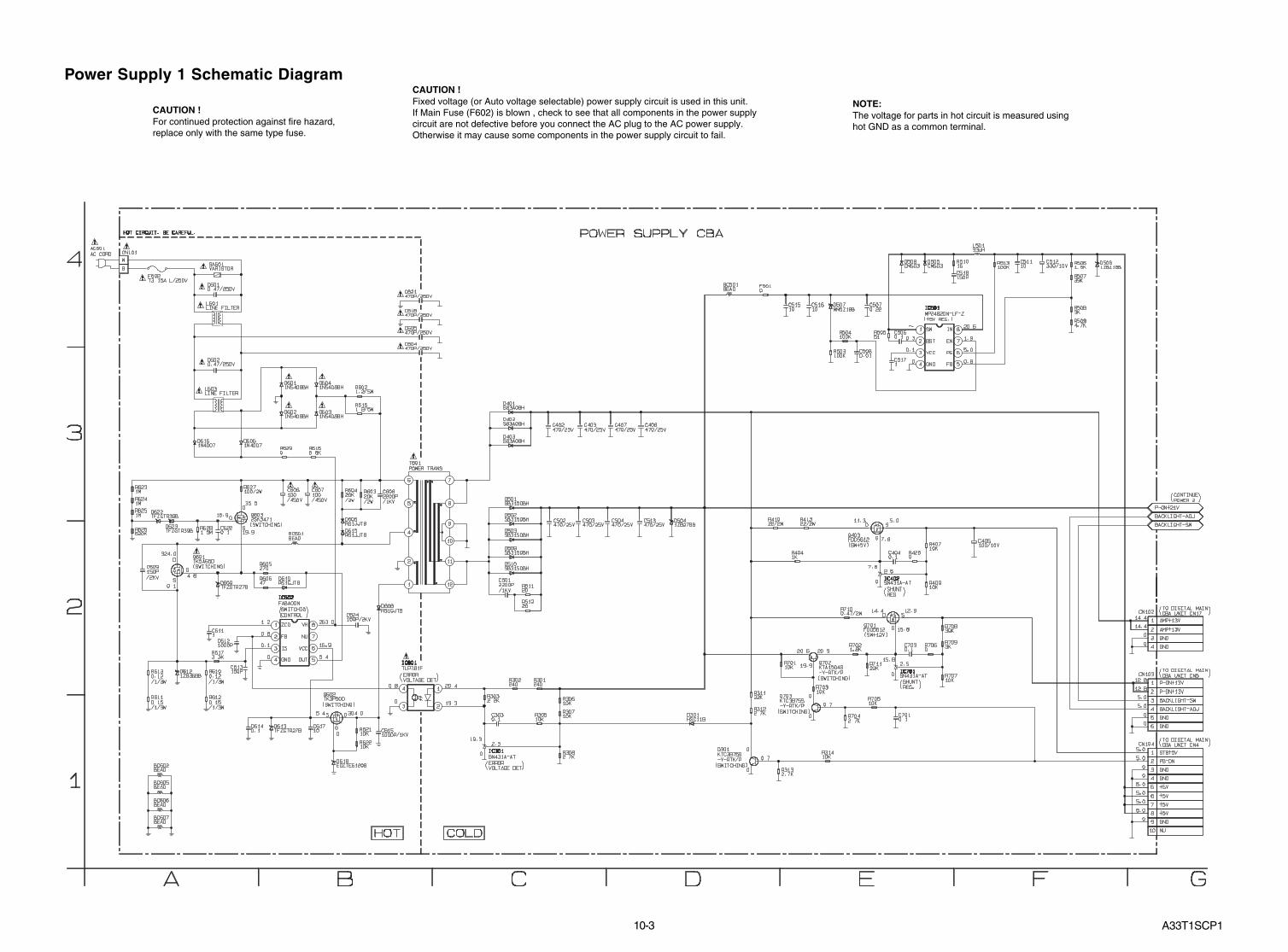
A33T1BLP
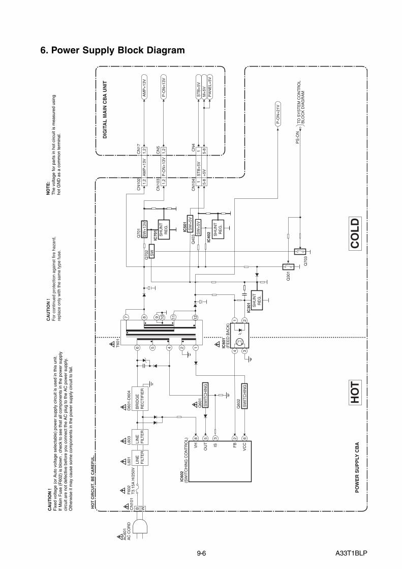
6. Power Supply Block DiagramC
AU
TIO
N !
For
con
tinue
d pr
otec
tion
agai
nst f
ire h
azar
d,re
plac
e on
ly w
ith th
e sa
me
type
fuse
.
10-1 LCDP_SC
SCHEMATIC DIAGRAMS / CBA AND TEST POINTS
Standard Notes
WARNING
Many electrical and mechanical parts in this chassis have special characteristics. These characteristics often pass unnoticed and the protection afforded by them cannot necessarily be obtained by using replacement components rated for higher voltage, wattage, etc. Replacement parts that have these special safety characteristics are identified in this manual and its supplements; electrical components having such features are identified by the mark “!” in the schematic diagram and the parts list. Before replacing any of these components, read the parts list in this manual carefully. The use of substitute replacement parts that do not have the same safety characteristics as specified in the parts list may create shock, fire, or other hazards.
Notes:1. Do not use the part number shown on these
drawings for ordering. The correct part number is shown in the parts list, and may be slightly different or amended since these drawings were prepared.
2. All resistance values are indicated in ohms (K = 103, M = 106).
3. Resistor wattages are 1/4W or 1/6W unless otherwise specified.
4. All capacitance values are indicated in F (P = 10-6 F).
5. All voltages are DC voltages unless otherwise specified.
6. Electrical parts such as capacitors, connectors, diodes, IC’s, transistors, resistors, switches, and fuses are identified by four digits. The first two digits are not shown for each component. In each block of the diagram, there is a note such as shown below to indicate these abbreviated two digits.
10-2 LCDP_SC
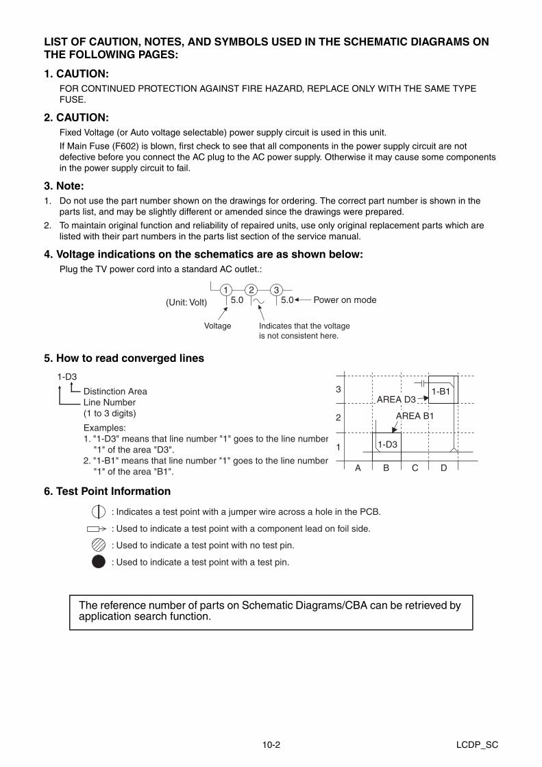
LIST OF CAUTION, NOTES, AND SYMBOLS USED IN THE SCHEMATIC DIAGRAMS ON THE FOLLOWING PAGES:
1. CAUTION:FOR CONTINUED PROTECTION AGAINST FIRE HAZARD, REPLACE ONLY WITH THE SAME TYPE FUSE.
2. CAUTION: Fixed Voltage (or Auto voltage selectable) power supply circuit is used in this unit.
If Main Fuse (F602) is blown, first check to see that all components in the power supply circuit are not defective before you connect the AC plug to the AC power supply. Otherwise it may cause some components in the power supply circuit to fail.
3. Note:1. Do not use the part number shown on the drawings for ordering. The correct part number is shown in the
parts list, and may be slightly different or amended since the drawings were prepared.
2. To maintain original function and reliability of repaired units, use only original replacement parts which are listed with their part numbers in the parts list section of the service manual.
4. Voltage indications on the schematics are as shown below:Plug the TV power cord into a standard AC outlet.:
5. How to read converged lines
6. Test Point Information
2 315.0 5.0
Voltage Indicates that the voltage is not consistent here.
Power on mode(Unit: Volt)
3
2
1
A B C D
1-B1
1-D3
AREA D3
AREA B1
1-D3
Distinction AreaLine Number (1 to 3 digits)
Examples:1. "1-D3" means that line number "1" goes to the line number "1" of the area "D3". 2. "1-B1" means that line number "1" goes to the line number "1" of the area "B1".
: Indicates a test point with a jumper wire across a hole in the PCB.
: Used to indicate a test point with a component lead on foil side.
: Used to indicate a test point with no test pin.
: Used to indicate a test point with a test pin.
The reference number of parts on Schematic Diagrams/CBA can be retrieved by application search function.
10-3
D501SB3150BH
10KR306
1N5408BHD603
CN101W
AC601AC CORD
1ZB36BBD612
1.2/5WR602
0.1C303
D401SB3A0BH
1N5408BHD602
0.47/250VC601
10KR307
IC301SN431A-AT
VARISTORSA601
4
3 2
1
IC601TLP781F
T3.15A L/250VF602
1N5408BHD601
TFZGTR27BD609
240R301
100/450V
C607
150P/2KV
C609
B
2.7KR308
0.15/1/3W
R611
270R605
240R302
10KR305
1N5408BHD604
470P/250VC621
C403470/25V
C402470/25V
C502470/25V
C503470/25V
1MR6241MR623
100/2WR627
1.5MR628
1MR625
620KR626 0.1
C622
TFZGTR39BD622
TFZGTR39BD623
20K/2W
R6032200P/1KV
C608
RS1JJTBD605
RS1JJTBD615
0.12/1/3W
R613
0.15/1/3W
R612
1000PC612
1C611
3.3KR617
150PC613
5
6
7
81
4
3
2
IC602FA8A00N
ZCD
GND OUT
VCC
NU
VH
IS
FB
47R606
RS1GJTBD610
1N4007D616
1N4007D606
6.8KR615
RS1GJTBD608
0.1C614
TFZGTR27BD613
10C617
D402SB3A0BH
D403SB3A0BH
C407470/25V
C408470/25V
2 PS-ON
7 +5V8 +5V
4 GND
CN1041 STB+5V
3 GND
6 +5V
10 NU
5 +5V
9 GND
5 GND
3 BACKLIGHT-SW
6 GND
4 BACKLIGHT-ADJ
2 P-ON+13V
CN1031 P-ON+13V
3 GND2 AMP+13V
4 GND
CN1021 AMP+13V
D502SB3150BH
D503SB3150BH
2200P/1KV
C501
20R511
C504470/25V
0.1C404
10KR409
IC402SN431A-AT
22/2WR410
22/2WR413
FDD5612Q403 G
D S
10KR407
L603LINE FILTER
0.47/250VC602
1.2/5WR616
20K/2W
R604100/450V
C606
1KR404
C405100/10V
0R426
20R512
EDZTE6120BD618
10KR621
10KR622
1000P/1KVC615
2.2KR303
D509SB3150BH
C513470/25V 1ZB27BB
D504
39KR708
0.1C703
FDD5612Q701 G
D S
10KR707
IC701SN431A-AT
0R706 3K
R709
0.47/2WR710
Q702KTA1504S-Y-RTK/P
1.8KR702
22KR71110K
R701
10KR703
Q703KTC3875S-Y-RTK/P
2.7KR704
10KR70522K
R311
2.7KR312
Q301KTC3875S-Y-RTK/P 10K
R314
2.7KR313
D301HSC119
P-ON+21V
BACKLIGHT-SWBACKLIGHT-ADJ
BEADBC501
10C515
10C516
MM5Z18BD507
100KR503
100KR504
0.01C508
5
6
7
81
4
3
2
IC501MP2482DN-LF-Z
SW
GND FB
PG
EN
IN
VCC
BST
0.22C507
L50133uH
10C511
100KR51316
R510
150PC518
0.1C506
51R505
1C517
1.5KR506
39KR507
C512330/10V
4.7KR5093KR508
1ZB11BBD506
0.12/1/3W
R610
TK5A65DQ601
G
D
S
L601LINE FILTER
470P/250VC618
470P/250VC604
0R629
470P/250VC605
150P/2KVC624
0F501
BC607BEAD
BC605BEAD
BC606BEAD
BC602BEAD
BC601BEAD
D510SB3150BH
0.1C701
CMS03D505
CMS03D508
6
5
4
2
1
7
8
9
10
11
12
T601POWER TRANS
2SK3471Q603G
D
S
TK3P50DQ602
G
DS
ERRORVOLTAGE DET
(SWITCHING)
HOT CIRCUIT. BE CAREFUL.
19.3
0.1
1
POWER SUPPLY CBA
2
A
TO DIGITAL MAINCBA UNIT CN4
FB C D E
3
G
4
HOT
19.3
COLD
0
2.5
4.8
324.0
0
0.8 20.4
(SWITCHING)
1.2
5.4
16.9
0
SWITCHIGCONTROL
0.1
263.0
0.8
00
0
00
00
2.5
SHUNTREG.
0
(SW+5V)
TO DIGITAL MAINCBA UNIT CN5
TO DIGITAL MAINCBA UNIT CN17
16.9
35.5
19.9
7.8
7.8
11.3 5.0
5.05.0
5.05.0
5.05.0
5.05.0
12.812.8
14.414.4
ERRORVOLTAGE DET
14.4
(SW+12V)
12.9
2.515.8
SHUNTREG.
15.8
0
(SWITCHING)(SWITCHING)
(SWITCHING)
(SWITCHING)
(+5V REG.)
CONTINUEPOWER 2
5.4 304.0
0
0
00.7
0
00.7
19.9
20.6 20.9
0.80
0.1
0.3
5.0
1.9
20.6
A33T1SCP1
Power Supply 1 Schematic Diagram
NOTE:The voltage for parts in hot circuit is measured using hot GND as a common terminal.
CAUTION !Fixed voltage (or Auto voltage selectable) power supply circuit is used in this unit. If Main Fuse (F602) is blown , check to see that all components in the power supply circuit are not defective before you connect the AC plug to the AC power supply. Otherwise it may cause some components in the power supply circuit to fail.
CAUTION !For continued protection against fire hazard,replace only with the same type fuse.
10-4
SK210TDD1001
100KR1021
330R1019
0.1C1018
240R1042
13KR1020
1
2
3
4
5
6
7
9
10
8
11
12 13
14
24
23
21
18
19
22
17
20
15
16
RT
CONTROLLOGIC
COMP
GND
NU
DRIVE
ISET
OVP
MCP
SEL
VIN
GND
LDO
DRIVE
DRIVE
DRIVE
DRIVE
DRIVE
DRIVE
DRIVE
IC1001HA7209PC
1C1020
4.7C1019
240R1006
100R1010
P-ON+21V
BACKLIGHT-SWBACKLIGHT-ADJ
5ILED3
CN1051VLED1
3ILED14ILED2
0R1017
22uHL1001
HSC119D1002
0.18/1WR1007
1000PC1017
200R1008
10R1009 Q1001
AP18T10AGH-HFG
D
S
10KR1002
0R1016
0R1018
2NU
1C1003
1C1004
100KR1004
13KR1030
1
2
3
4
5
6
7
9
10
8
11
12 13
14
24
23
21
18
19
22
17
20
15
16
RT
CONTROLLOGIC
COMP
GND
NU
DRIVE
ISET
OVP
MCP
SEL
VIN
GND
LDO
DRIVE
DRIVE
DRIVE
DRIVE
DRIVE
DRIVE
DRIVE
IC1002HA7209PC
1C1027
0R1024
1000PC1025
240R1040
0R1022
0.18/1WR1039
100R1036
10R1037
22uHL1002
240R1041
100KR1031
Q1002AP18T10AGH-HFG
D
S
4.7C1029
200R1038
330R1029
HSC119D1004
1000PC1031
0R1023
SK210TDD1003
0.1C1028
10KR1003
100KR1005
1000PC1038
0R1028
6NU7ILED48ILED59ILED610NU11VLED2
1KR1047
0R1032
1C1023
1/100VC1011
1/100VC1010
510KR1013
430KR1014
27KR1015
1/100VC1012
1/100VC1013
510KR1025
430KR1026
27KR1027
1KR1035
0R1012
10R1045
220P/100VC1041
10R1046
220P/100VC1040
0R1033
1000PC1024
1000PC1022
1C1006
47/100VC1015
47/100VC1007
330/25V
C1002330/25V
C100147/100VC1008
47/100VC1016
POWER SUPPLY CBA
1
2
3
4
H LKJI M
4.9
0
1.6
0
17.6
0
4.9
0
0.1
4.4
0
0.5
0.6
1.0
1.3
1.4
0
4.5
0
0
0
0.6
LED BACKLIGHTDRIVER
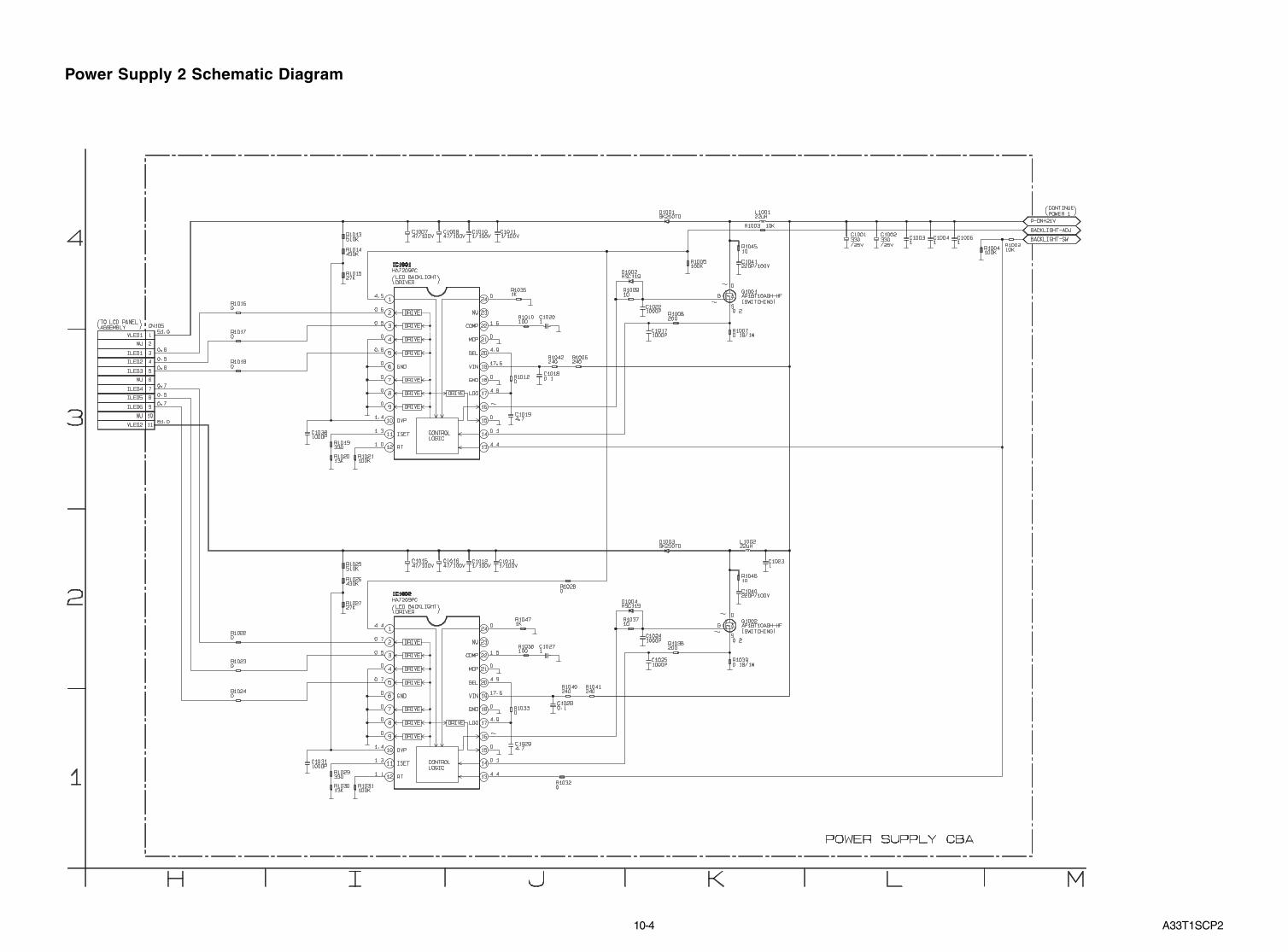
CONTINUEPOWER 1
TO LCD PANELASSEMBLY
0.2(SWITCHING)
0
0.1
4.4
4.4
1.3
4.9
0.5
0
1.4
17.6
0
4.9
0
0
0
0
0
1.1
0
0.2
LED BACKLIGHTDRIVER
0.7
1.5
0.7
(SWITCHING)
51.0
0.60.50.6
0.70.50.7
51.0
A33T1SCP2
Power Supply 2 Schematic Diagram
10-5
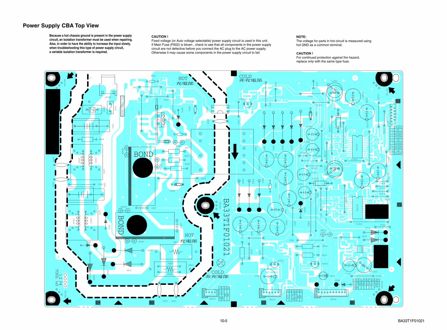
Power Supply CBA Top View
BA33T1F01021
NOTE:The voltage for parts in hot circuit is measured using hot GND as a common terminal.
Because a hot chassis ground is present in the power supply circuit, an isolation transformer must be used when repairing.Also, in order to have the ability to increase the input slowly, when troubleshooting this type of power supply circuit, a variable isolation transformer is required.
CAUTION !Fixed voltage (or Auto voltage selectable) power supply circuit is used in this unit. If Main Fuse (F602) is blown , check to see that all components in the power supply circuit are not defective before you connect the AC plug to the AC power supply. Otherwise it may cause some components in the power supply circuit to fail. CAUTION !
For continued protection against fire hazard,replace only with the same type fuse.
IC602
IC1001
IC1002
IC501
T3.15AL/250V
BOND
BOND
DC
J701
J702
J703
J1020
J1021
J1022
J1023
J1024
R602
R603
R410
R604
R413
R608
R616
L1001
L1002
R627
C401
C402
C403
C405
C407
C408
C601
C602
C604
C605
C606
C607
C608
C609
GP1001
GP1002
GP1003
GP1004
GP1005
C615
C618
C621 C623
C624
D401
D402
D403
D601
D602
D603
D604
D606
L501
D612
D616
IC402
BC501
IC601
T601
C1001
C1002
C1007 C1008
J401
J402
J403
J404
B19
C1015 C1016
J601
J602
J603
J604
J605
J606
J610
CN101
CN102 CN103 CN104
CN105
R1007
JS601
JS602
JS603
JS604
JS606
JS607
R710
C1042
C1043
C501
R1039
C502
C503
C504
C701C512
C513
F602
SA601
D501
D502
D503
D504
Q601
D506
D509
D510
D512
D513
IC301
L601
L603
BC601
BC602
BC605
BC606
BC607
IC701
J1001
J1003
J1004
J1005
J301
J1006
J302
J1007
J1008
J304
J1009
J115
J1010
J501
J1011
J1012
J1013
J1014
J1015
J1016
J1017
J1018
J1019
1 2 4
COLD
COLD
1234
567
1 2 3 4 5 6
+13V
+13V
BL-SW
BL-ADJ
GND
GND
VLED1NC
ILED1ILED2
ILED4
HOT
HOT
+13V AMP
+13V AMP
GND
GND
1 2 3 4
89
1011
ILED5ILED6NC
VLED2
ILED3NC
1 2 3 4 5 6 7 8 9
+5VSb
PS-ON
GND
GND
+5V
+5V
+5V
+5V
GND
NC
10
3
BA33T1F01021
TOOL NO
1234
10-6
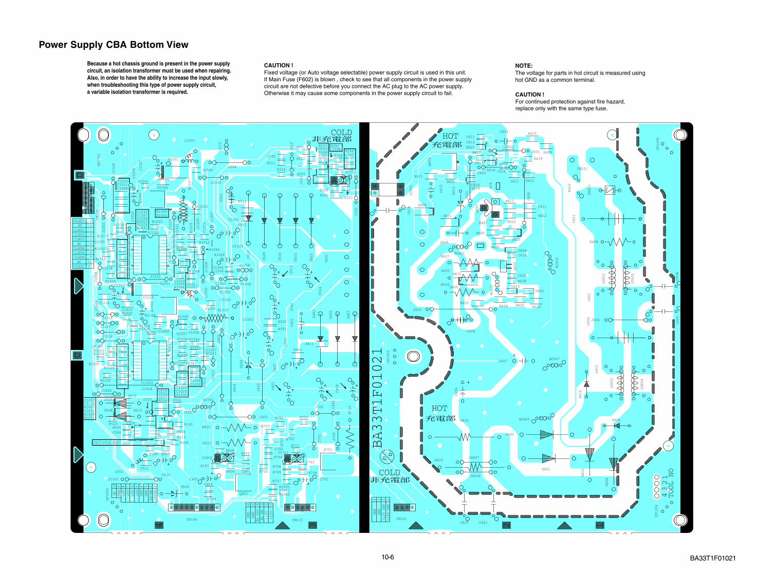
Power Supply CBA Bottom View
BA33T1F01021
NOTE:The voltage for parts in hot circuit is measured using hot GND as a common terminal.
Because a hot chassis ground is present in the power supply circuit, an isolation transformer must be used when repairing.Also, in order to have the ability to increase the input slowly, when troubleshooting this type of power supply circuit, a variable isolation transformer is required.
CAUTION !Fixed voltage (or Auto voltage selectable) power supply circuit is used in this unit. If Main Fuse (F602) is blown , check to see that all components in the power supply circuit are not defective before you connect the AC plug to the AC power supply. Otherwise it may cause some components in the power supply circuit to fail. CAUTION !
For continued protection against fire hazard,replace only with the same type fuse.
DC
J701
J702
J703
J1020
J1021
J1022
J1023
J1024
R602
R603
R410
R604
R413
R608
R616
L1001
L1002
R627
C401
C402
C403
C405
C407
C408
C601
C602
C604
C605
C606
C607
C608
C609
GP1001
GP1002
GP1003
GP1004
GP1005
C615
C618
C621C623
C624
D401
D402
D403
D601
D602
D603
D604
D606
L501
D612
D616
IC402
BC501
IC601
T601
C1001
C1002
C1007
C1008
J401
J402
J403
J404
B19
C1015
C1016
J601
J602
J603
J604
J605
J606
J610
CN101
CN102CN103CN104
CN105
R1007
JS601
JS602
JS603
JS604
JS606
JS607
R710
C1042
C1043C501
R1039 C502
C503
C504
C701C512
C513
F602
SA601
D501
D502
D503
D504
Q601
D506
D509
D510
D512
D513
IC301
L601
L603
BC601
BC602
BC605
BC606
BC607
IC701
J1001
J1003
J1004
J1005
J301
J1006
J302
J1007
J1008
J304
J1009
J115
J1010
J501
J1011
J1012 J1013
J1014
J1015
J1016
J1017
J1018
J1019
124
COLD
COLD
1234
567
123456
+13V
+13V
BL-SW
BL-ADJ
GND
GND
VLED1NC
ILED1ILED2
ILED4
HOT
HOT
+13V AMP
+13V AMP
GND
GND
1234
89
1011
ILED5ILED6NC
VLED2
ILED3NC
123456789
+5VSb
PS-ON
GND
GND
+5V
+5V
+5V
+5V
GND
NC
10
3
BA33T1F01021
TOOL NO
12
34
R401
R404
R407
R409
R411
R605
R606
R607 R610
R611
R612
R613
R615
R617
R619
R426
R621
R622
R623R624 R625 R626
R628
R629
C404
C406
C610
C611
C612
C613
C614
C617C620
F501
C622
Q301
Q701
D605
Q702
Q703
D608
D609
D610
D611
D613
D614
D615
D618
D621
D622
IC602
D623C1003
C1004
C1005
Q1001
C1006
Q1002
C1009
C1010C1011
C1012
C1013
C1014
C1017
C1018
R301
C1019
R302R303
R304
R305
R306
R307
R308
C1020
C1021
C1022
C1023
C1024
D1001
R501
C1025
D1002
R502
C1026
R503
D1003
C1027
R504
D1004
C1028
R311
R505
C1029
R506
R1002
R312R313
R507
R1003
R314
R508
R1004
R509
R1005
R1006
R1008
C1030
R1009
R701
IC1001
C1031
R702
IC1002
C1032
R703
C1033
R510
R704
C1034
R511
R705
C1035
C1036
R706
R512
R707
R513
C1037
R708
R1010
C1038
R709
C1039
R1012
R1013
R1014
R1015R1016
R1017
C1040
R1018
C1041
R711
R1019
R1020
R1021
R1022
R1023R1024
R1025R1026
R1027
R1028
R1029
C302
C303
C304
R1030
C305
R1031
R1032
R1033
R1034
R1035
R1036
R1037
R1038
C506
C507
C508
R1040
R1041
R1042R1044
R1045
R1046
C702
R1047
C703
C704
C511
C514
C515C516
C517
C518
D301
Q403
D505
Q602
D507
Q603
D508
IC501

A33T1WI11-1
WIRING DIAGRAMTU
NE
R U
NIT
DIG
ITA
L M
AIN
CB
A U
NIT
CO
MP
ON
EN
T-Y
-IN
CO
MP
ON
EN
T-P
b-IN
CO
MP
ON
EN
T-P
r-IN VID
EO
-IN
AU
DIO
(L)-
IN
AU
DIO
(R)-
INR
EA
R
DIG
ITA
L A
UD
IO-O
UT
(CO
AX
IAL)
HD
MI-I
N1
HD
MI-I
N2
PC
-RG
B-IN
US
B J
AC
K
SC
AR
T JA
CK
CI C
AR
D
SLO
T
SID
E
PC
-AU
DIO
-IN
HE
AD
PH
ON
EJA
CK
PO
WE
R S
UP
PLY
CB
A
LCD
PA
NE
L A
SS
EM
BLY
CN
101
BW
AC
601
AC
CO
RD
21 2317 19 24 25 26 27 28 29 30 31 32 33 34 35 36 37 38 39 402220181612 148 10 151311973 5 621 4
VC
C-P
anel
VC
C-P
anel
VC
C-P
anel
GN
DG
ND
GN
D
RX
O0(
+)R
XO
0(-)
RX
O1(
+)R
XO
1(-)
RX
O2(
+)R
XO
2(-)
GN
DG
ND
RX
OC
(+)
RX
OC
(-)
RX
O3(
+)R
XO
3(-)
RX
E0(
+)R
XE
0(-)
RX
E1(
+)R
XE
1(-)
RX
E2(
+)R
XE
2(-)
GN
DG
ND
RX
EC
(+)
RX
EC
(-)
RX
E3(
+)R
XE
3(-)
GN
DG
ND
CO
N1
DIS
PLA
YV
SE
L1V
SE
L2
RX
O4(
+)R
XO
4(-)
RX
E4(
+)R
XE
4(-)
CN
7
64 53214321
6 7 84 5321C
N3
FUN
CTI
ON
CB
A U
NIT
+5V
LED
-R
RE
MO
TEG
ND
IR-K
EY
SP
(L)+
SP
(R)+
SP
(L)-
SP
(R)-
SD
A(N
U)
SC
L(N
U)
NU
+5V
LED
-R
RE
MO
TEG
ND
IR-K
EY
NU
CN
18S
P38
01S
PE
AK
ER
L-C
H
SP
3802
SP
EA
KE
RR
-CH
CN
4
CN
12
CN
104
1 2 3 4 5 6 2 3 4 5 6
2 3 45 6
7
CN
105 1 2 3 4 5 6 7 8 9 10 11
8 9 10
1 2 3 4 5 6 7 8 9 10
STB
+5V
VLE
D1
VLE
D2
NU
ILE
D1
ILE
D2
ILE
D3
NU
ILE
D4
ILE
D5
ILE
D6
NU
PS
-ON
CN
5
CN
102
CN
103
1
12 3 41P
-ON
+13V
2 3 4
CN
17 1A
MP
+13V
AM
P+1
3V
P-O
N+1
3VB
AC
KLI
GH
T-S
WB
AC
KLI
GH
T-A
DJ
GN
DG
ND
PAN
EL+
5VPA
NE
L+5V
+5V
+5V
NU
GN
D
GN
DG
ND
GN
DG
ND
CL1
2
CL4
CL5
CL1
7
CL1
8
CL7

12-1 A33T1 CEX
EXPLODED VIEWS
Cabinet
A1
A6
A4
A9
L9
B12
SP3802
SP3801
L9
L9
L27SSK1
LCD1
A13
L23
B18B17
B17
A3
L27
A15
S7
SSK1
SBA1
Function CBA Unit
Power Supply CBA
Digital Main CBA Unit
See Electrical Parts Listfor parts with this mark.
A19
L23
AC601
L9 SNA1
CL7
B19L35
CL18
L23
CL4CL5CL17
L9CL12
B10L67

12-2 A33T1 PEX
Packing
S4
S7
Packing Tape
Packing Tape
Packing Tape
SBA1
Some Ref. Numbers are not in sequence.
S3
X3 A17 X19X4
SSK1
X2
S1
Tape
Tape
X1
SNA1
S6

2013/05/09 13-1 A33T1_CA.fm
MECHANICAL PARTS LIST
PRODUCT SAFETY NOTE: Products marked with a ! have special characteristics important to safety. Before replacing any of these components, read carefully the product safety notice in this service manual. Don’t degrade the safety of the product through improper servicing.
NOTE: Parts that are not assigned part numbers (---------) are not available.
LCD PANEL ASSEMBLY
Ref. No. Mark Description Part No.
A3! REAR COVER A33T1EP 1EM128055
B17 WALL MOUNT BRACKET A11N0UH 1EM434637
B18 WALL MOUNT COVER A2170UT 1EM332137
PACKINGS6 SET BAG A21P6UH 1EM334729
ACCESSORYX3 REMOTE CONTROL UNIT NH217RD NH217RD
Ref. No. Mark Description Part No.
A13 JACK HOLDER(MHL) A33T1EP 1EM228183
A15! RATING LABEL A33T1EP ----------
A17 ENERGY LABEL A33T1EP ----------
A19 POP LABEL A33T1EP ----------
AC601! AC CORD W/O A GND WIRE CEE/1700/NO/BLACK
WAE172ZHN010
B10 STAND HOLDER A31T0UH 1EM127914
CL4 WIRE ASSEMBLY 10PIN 10PIN/95MM WX1A33T1C301
CL5 WIRE ASSEMBLY 6PIN 6PIN/70MM WX1A33T1C302
CL7 WIRE ASSEMBLY 5PIN SENSOR 5PIN/110MM
WX1A33T1C107
CL17 WIRE ASSEMBLY 4PIN 4PIN/65MM WX1A33T1C303
CL18 WIRE ASSEMBLY SP 4PIN 4PIN/330MM/100MM
WX1A33T1C204
L9 SCREW P-TIGHT 3X12 BIND HEAD+ BLK
GBHP3120
L23 SCREW S-TIGHT M3X6 BIND HEAD+ GBJS3060
L27 SCREW S-TIGHT M3X8 BIND HEAD+ GBHS3080
L67 SCREW S-TIGHT M3X10 BIND HEAD+ GBJS3100
SBA1 STAND BASE ASSEMBLY A33T1EP 1EM030625
SNA1 STAND NECK ASSEMBLY A33T1EP 1EM030626
SP3801 SPEAKER MAGNETIC 8/8W S0310F15 DS08110XQ003
SP3802 SPEAKER MAGNETIC 8/8W S0310F15 DS08110XQ003
SSK1 STAND SCREW KIT A33T1EP(DOUBLE SEMS SCREW M4X20 + BLK)
2ESA00116
PACKINGS1 CARTON A33T1EP 1EM335158
S3 STYROFOAM TOP A33T1EP 1EM031046
S4 STYROFOAM BOTTOM A33T1EP 1EM031047
S7 SERIAL NO. LABEL A33M1EP ----------
ACCESSORIESX1 BAG POLYETHYLENE 235X365XT0.03 0EM408420A
X2! OWNERS MANUAL A33M1EP 1EMN30383A
X4 BATTERY DRY R03(SIZE AAA ) XB00M0RKT001
X19 SAFETY AND WARRANTY BOOK A23F0EP
1EMN30040
Ref. No. Mark Description Part No.
LCD1! LCD PANEL ASSEMBLY U30T3F0
Consists of the following
A1! FRONT CABINET A33T1EP 1EM128054
A4! X -PCB COVER A31T0UH 1EM228323
A6 CONTROL PLATE A31F0UT 1EM334317
A9 SENSOR LENS A31F0UT 1EM334217
B12 SHIELD PLATE A31F0UT 1EM334218
CL12 WIRE ASSEMBLY LVDS 39W 40PIN/250MM
WX1A33T1C106
L9 SCREW P-TIGHT 3X12 BIND HEAD+ BLK
GBHP3120
LCD MODULE 39INCH ----------
2013/05/09 14-1 A33T1_EL.fm
ELECTRICAL PARTS LIST
PRODUCT SAFETY NOTE: Products marked with a ! have special characteristics important to safety. Before replacing any of these components, read carefully the product safety notice in this service manual. Don't degrade the safety of the product through improper servicing.
NOTES:
1. Parts that are not assigned part numbers (---------) are not available.
2. Tolerance of Capacitors and Resistors are noted with the following symbols.
POWER SUPPLY CBA
C.....±0.25% D.....±0.5% F.....±1%
G.....±2% J......±5% K.....±10%
M.....±20% N.....±30% Z.....+80/-20%
Ref. No. Description Part No.
PWR1 POWER SUPPLY CBA A33T1MPW-001
Consists of the following
CAPACITORSC303 CAP CHIP 1608 K/X7R/0.1F/50V CHD104EYA032
C402 CAP ELE 470F/25V/M/85 CED4710V8006
C403 CAP ELE 470F/25V/M/85 CED4710V8006
C404 CAP CHIP 1608 K/X7R/0.1F/50V CHD104EYA032
C405 CAP ELE 100F/10V/M/85 CEB1010V8006
C407 CAP ELE 470F/25V/M/85 CED4710V8006
C408 CAP ELE 470F/25V/M/85 CED4710V8006
C501 CERAMIC CAP. 2200pF/1kV CCD3AKA0R222
C502 ELECTROLYTIC CAP. 470F/25V M(105C) CE1EMASTH471
C503 ELECTROLYTIC CAP. 470F/25V M(105C) CE1EMASTH471
C504 ELECTROLYTIC CAP. 470F/25V M(105C) CE1EMASTH471
C506 CAP CHIP 1608 K/X7R/0.1F/50V CHD104EYA032
C507 CHIP CERAMIC CAP.(1608) F Z 0.22F/50V CHD1JZ30F224
C508 CHIP CERAMIC CAP.(1608) B K 0.01F/50V CHD1JK30B103
C511 CHIP CERAMIC CAP. B K 10F/10V CHE1AK30B106
C512 CAP ELE 105 330F/10V/M/105 CED3310S6009
C513 ELECTROLYTIC CAP. 470F/25V M(105C) CE1EMASTH471
C515 CAP CHIP 3216 B K 10F/25V CA1E106MR082
C516 CAP CHIP 3216 B K 10F/25V CA1E106MR082
C517 CHIP CERAMIC CAP.(1608) B K 1F/25V CHD1EK30B105
C518 CHIP CERAMIC CAP. CH J 150pF/50V CHD1JJ3CH151
C601! CAP METALLIZED FILM 0.47F/250V/K/MPX CTA474EUR001
C602! CAP METALLIZED FILM 0.47F/250V/K/MPX CTA474EUR001
C604! CAP CERAMIC 470pF/250V KX CA2E471MR100
C605! CAP CERAMIC 470pF/250V KX CA2E471MR100
C606! CAP ELE 100F/450V/M/105 CV9E101M02W1
C607! CAP ELE 100F/450V/M/105 CV9E101M02W1
C608 CERAMIC CAP. 2200pF/1kV CCD3AKA0R222
C609 CERAMIC CAP. 150pF/2kV CA3D151PAN04
C611 CHIP CERAMIC CAP.(1608) B K 1F/25V CHD1EK30B105
C612 CHIP CERAMIC CAP.(1608) B K 1000pF/50V CHD1JK30B102
C613 CHIP CERAMIC CAP. CH J 150pF/50V CHD1JJ3CH151
C614 CAP CHIP 1608 K/X7R/0.1F/50V CHD104EYA032
C615 CAP CERAMIC HV 1000pF/1kV B K CA3A102TE006
C617 CAP CHIP 3216 B K 10F/25V CA1E106MR082
C618! CAP CERAMIC 470pF/250V KX CA2E471MR100
C621! CAP CERAMIC 470pF/250V KX CA2E471MR100
C622 CAP CHIP 1608 K/X7R/0.1F/50V CHD104EYA032
C624 CERAMIC CAP. 150pF/2kV CA3D151PAN04
C703 CAP CHIP 1608 K/X7R/0.1F/50V CHD104EYA032
C704 CAP CHIP 1608 K/X7R/0.1F/50V CHD104EYA032
C1001 ELECTROLYTIC CAP. 330F/25V (RJ4) CED331ELN026
C1002 ELECTROLYTIC CAP. 330F/25V (RJ4) CED331ELN026
C1003 CHIP CERAMIC CAP.(1608) B K 1F/25V CHD1EK30B105
C1004 CHIP CERAMIC CAP.(1608) B K 1F/25V CHD1EK30B105
C1006 CHIP CERAMIC CAP.(1608) B K 1F/25V CHD1EK30B105
C1007 ELECTROLYTIC CAP SK100M470YZZP50R CE2AMASTH470
C1008 ELECTROLYTIC CAP SK100M470YZZP50R CE2AMASTH470
C1010 CHIP CERAMIC CAP.(3216) X7R K 1.0F/100V CA2A105MR080
C1011 CHIP CERAMIC CAP.(3216) X7R K 1.0F/100V CA2A105MR080
C1012 CHIP CERAMIC CAP.(3216) X7R K 1.0F/100V CA2A105MR080
C1013 CHIP CERAMIC CAP.(3216) X7R K 1.0F/100V CA2A105MR080
C1015 ELECTROLYTIC CAP SK100M470YZZP50R CE2AMASTH470
C1016 ELECTROLYTIC CAP SK100M470YZZP50R CE2AMASTH470
C1017 CHIP CERAMIC CAP.(1608) B K 1000pF/50V CHD1JK30B102
C1018 CHIP CERAMIC CAP.(1608) F Z 0.1F/50V CHD1JZ30F104
C1019 CHIP CERAMIC CAP.(1608) B K 4.7F/6.3V CHD0KK30B475
C1020 CHIP CERAMIC CAP.(1608) B K 1F/25V CHD1EK30B105
C1022 CHIP CERAMIC CAP.(1608) B K 1000pF/50V CHD1JK30B102
C1023 CHIP CERAMIC CAP.(1608) B K 1F/25V CHD1EK30B105
C1024 CHIP CERAMIC CAP.(1608) B K 1000pF/50V CHD1JK30B102
C1025 CHIP CERAMIC CAP.(1608) B K 1000pF/50V CHD1JK30B102
C1027 CHIP CERAMIC CAP.(1608) B K 1F/25V CHD1EK30B105
C1028 CHIP CERAMIC CAP.(1608) F Z 0.1F/50V CHD1JZ30F104
C1029 CHIP CERAMIC CAP.(1608) B K 4.7F/6.3V CHD0KK30B475
C1031 CHIP CERAMIC CAP.(1608) B K 1000pF/50V CHD1JK30B102
C1038 CHIP CERAMIC CAP.(1608) B K 1000pF/50V CHD1JK30B102
C1040 CHIP CERAMIC CAP.(1608) C0G/J/220pF/100V CA2A221MR133
C1041 CHIP CERAMIC CAP.(1608) C0G/J/220pF/100V CA2A221MR133
CONNECTORS
CN101! CONNECTOR S2P3-VH (LF)(SN) JCVHC02JG002
CN102 CONNECTOR PRINT OSU JS-1125-04(K) J3JT04CHY001
CN103 PH CONNECTOR TOP 6P B6B-PH-K-S (LF)(SN)
J3PHC06JG029
CN104 PH CONNECTOR TOP 10P B10B-PH-K-S(LF)(SN)
J3PHC10JG029
CN105 FFC CONNECTOR IMSA-9615S-11A-PP-A JC96J11ER007
DIODESD301 DIODE SWITCHING HSC119 TRF -E QD1Z00HSC119
D401 DIODE SCHOTTKY SB3A0BH NDWZ000SB3A0
D402 DIODE SCHOTTKY SB3A0BH NDWZ000SB3A0
D403 DIODE SCHOTTKY SB3A0BH NDWZ000SB3A0
D501 DIODE SCHOTTKY SB3150BH NDWZ00SB3150
D502 DIODE SCHOTTKY SB3150BH NDWZ00SB3150
D503 DIODE SCHOTTKY SB3150BH NDWZ00SB3150
D504 DIODE ZENER 1ZB27BB NDWZ0001ZB27
D505 DIODE CMS03(TE12L Q) QD1Z00CMS03Q
D506 DIODE ZENER 1ZB11BB NDWZ0001ZB11
D507 ZENER DIODE MM5Z18B ND1B0MM5Z18B
D508 DIODE CMS03(TE12L Q) QD1Z00CMS03Q
D509 DIODE SCHOTTKY SB3150BH NDWZ00SB3150
D510 DIODE SCHOTTKY SB3150BH NDWZ00SB3150
D601! DIODE RECTIFIEY 1N5408BH NDL2001N5408
D602! DIODE RECTIFIEY 1N5408BH NDL2001N5408
D603! DIODE RECTIFIEY 1N5408BH NDL2001N5408
D604! DIODE RECTIFIEY 1N5408BH NDL2001N5408
D605 DIODE FAST RECOVERY RS1JJTB ND1Z0RS1JJTB
D606 RECTIFIER DIODE 1N4007 NDQZ001N4007
D608 DIODE FAST RECOVERY RS1GJTB ND1Z0RS1GJTB
D609 ZENER DIODE SMD TFZGTR27B QD1B000TFZ27
D610 DIODE FAST RECOVERY RS1GJTB ND1Z0RS1GJTB
D612 DIODE ZENER 1ZB36BB NDWZ0001ZB36
D613 ZENER DIODE SMD TFZGTR27B QD1B000TFZ27
Ref. No. Description Part No.
2013/05/09 14-2 A33T1_EL.fm
D615 DIODE FAST RECOVERY RS1JJTB ND1Z0RS1JJTB
D616 RECTIFIER DIODE 1N4007 NDQZ001N4007
D618 ZENER DIODE EDZTE61 20B QD1B000EDZ20
D622 ZENER DIODE SMD TFZGTR39B QD1B000TFZ39
D623 ZENER DIODE SMD TFZGTR39B QD1B000TFZ39
D1001 DIODE SCHOTTKY SMD SK210TD ND1Z0SK210TD
D1002 DIODE SWITCHING HSC119 TRF -E QD1Z00HSC119
D1003 DIODE SCHOTTKY SMD SK210TD ND1Z0SK210TD
D1004 DIODE SWITCHING HSC119 TRF -E QD1Z00HSC119
ICSIC301 IC SHUNT REGULATOR SN431A-AT NQSZ00SN431A
IC402 IC SHUNT REGULATOR SN431A-AT NQSZ00SN431A
IC501 IC DCDC CONVERTER MP2482DN-LF-Z/SOIC8/
NSCA0T09M005
IC601! IC PHOTOCOUPLER TLP781F(D4-FUNBLL F) QPEL781FBLLF
IC602 IC SWITCHING FA8A00N/SOP-8/8PIN QSCA0T0FD010
IC701 IC SHUNT REGULATOR SN431A-AT NQSZ00SN431A
IC1001 IC LED BACKLIGHT CONTROLLER HA7209PC/SOP/24PIN
NSCA0T00H003
IC1002 IC LED BACKLIGHT CONTROLLER HA7209PC/SOP/24PIN
NSCA0T00H003
COILSL501 COIL POWER INDUCTORS DIP RCR1010NP-
330M/33HLLF3300SF012
L601! COIL LINE FILTER JLB20154/18MH LLEG0Z0XB022
L603! COIL LINE FILTER JLB20154/18MH LLEG0Z0XB022
L1001 POWER INDUCTORS 22UH/ST0812DR9*12-00 LLF2200Y2004
L1002 POWER INDUCTORS 22UH/ST0812DR9*12-00 LLF2200Y2004
TRANSISTORSQ301 CHIP TRANSISTOR KTC3875S-Y-RTK/P NQ1YKTC3875S
Q403 FET MOS FDD5612/Z NF2ZFDD56120
Q601! FET MOS TK5A65D LS1FNDQ(M QEEZTK5A65DM
Q602 FET MOS TK3P50D RQ(S QF2Z0TK3P50D
Q603 FET MOS 2SK3471 TE12L F QF1Z02SK3471
Q701 FET MOS FDD5612/Z NF2ZFDD56120
Q702 CHIP TRANSISTOR KTA1504S-Y-RTK/P NQ1YKTA1504S
Q703 CHIP TRANSISTOR KTC3875S-Y-RTK/P NQ1YKTC3875S
Q1001 FET MOS SMD AP18T10AGH-HF NF2Z18T10AGH
Q1002 FET MOS SMD AP18T10AGH-HF NF2Z18T10AGH
RESISTORSR301 RES CHIP 3216 1/4W J 240 RRX4241YF004
R302 RES CHIP 3216 1/4W J 240 RRX4241YF004
R303 RES CHIP 1608 1/10W F 2.20k RTW2201HH008
R305 RES CHIP 1608 1/10W F 10.0k RTW1002HH008
R306 RES CHIP 1608 1/10W F 10.0k RTW1002HH008
R307 RES CHIP 1608 1/10W F 10.0k RTW1002HH008
R308 RES CHIP 1608 1/10W F 2.70k RTW2701HH008
R311 RES CHIP 1608 1/10W F 22.0k RTW2202HH008
R312 RES CHIP 1608 1/10W F 2.70k RTW2701HH008
R313 RES CHIP 1608 1/10W F 2.70k RTW2701HH008
R314 RES CHIP 1608 1/10W J 10k RRXA103HH013
R404 RES CHIP 1608 1/10W F 1.00k RTW1001HH008
R407 RES CHIP 1608 1/10W F 10.0k RTW1002HH008
R409 RES CHIP 1608 1/10W F 10.0k RTW1002HH008
R410 METAL OXIDE FILM RES. 2W J 22 RN02220ZU001
R413 METAL OXIDE FILM RES. 2W J 22 RN02220ZU001
R426 RES CHIP 1608 1/10W 0 RRXA000HH014
R503 RES CHIP 1608 1/10W J 100k RRXA104HH013
R504 RES CHIP 3216 1/4W J 100k RRX4104HH034
R505 RES CHIP 1608 1/10W J 51 RRXA510HH013
R506 RES CHIP 1608 1/10W F 1.50k RTW1501HH008
R507 CHIP RES. 1/10W F 39k RRXAFR5H3902
R508 CHIP RES. 1/10W F 3k RRXAFR5H3001
R509 RES CHIP 1608 1/10W F 4.70k RTW4701YF002
R510 RES CHIP 1608 1/10W J 16 RRXA160HH013
R511 RES CHIP 3216 1/4W J 20 RRX4200HH034
R512 RES CHIP 3216 1/4W J 20 RRX4200HH034
Ref. No. Description Part No.
R513 RES CHIP 1608 1/10W F 100k RTW1003HH008
R602 RES CEMENT 5W/J/1.2 RWJ1R2PAK007
R603 METAL OXIDE FILM RES. 2W J 20k RN02203ZU001
R604 METAL OXIDE FILM RES. 2W J 20k RN02203ZU001
R605 RES CHIP 3216 1/4W J 270 RRX4271YF004
R606 RES CHIP 3216 1/4W J 47 RRX4470YF004
R610 RES CHIP 3216 1/3W J 0.12 RRJR12RYL008
R611 RES CHIP 3216 1/3W J 0.15 RRJR15RYL008
R612 RES CHIP 3216 1/3W J 0.15 RRJR15RYL008
R613 RES CHIP 3216 1/3W J 0.12 RRJR12RYL008
R615 RES CHIP 3216 1/4W J 6.8k RRX4682YF004
R616 RES CEMENT 5W/J/1.2 RWJ1R2PAK007
R617 RES CHIP 1608 1/10W J 3.3k RRXA332HH013
R621 RES CHIP 3216 1/4W J 10k RRX4103HH034
R622 RES CHIP 3216 1/4W J 10k RRX4103HH034
R623 RES CHIP 3216 1/4W J 1.0M RRX4105HH034
R624 RES CHIP 3216 1/4W J 1.0M RRX4105HH034
R625 RES CHIP 3216 1/4W J 1.0M RRX4105HH034
R626 RES CHIP 3216 1/4W J 620k RRX4624HH034
R627 METALOXIDE RES 2W J 100 RNJ101PAK002
R628 RES CHIP 1608 1/10W J 1.5M RRXA155HH013
R629 RES CHIP 3216 1/4W J 0 RRJ000WAL004
R701 RES CHIP 1608 1/10W J 10k RRXA103HH013
R702 RES CHIP 1608 1/10W J 1.8k RRXA182HH013
R703 RES CHIP 1608 1/10W J 10k RRXA103HH013
R704 RES CHIP 1608 1/10W F 2.70k RTW2701HH008
R705 RES CHIP 1608 1/10W J 10k RRXA103HH013
R706 RES CHIP 1608 1/10W 0 RRXA000HH014
R707 RES CHIP 1608 1/10W F 10.0k RTW1002HH008
R708 CHIP RES. 1/10W F 39k RRXAFR5H3902
R709 CHIP RES. 1/10W F 3k RRXAFR5H3001
R710 METAL OXIDE FILM RES. 2W J 0.47 RN02R47ZU001
R711 RES CHIP 1608 1/10W F 22.0k RTW2202HH008
R1002 RES CHIP 1608 1/10W J 10k RRXA103HH013
R1003 RES CHIP 1608 1/10W J 10k RRXA103HH013
R1004 RES CHIP 1608 1/10W J 100k RRXA104HH013
R1005 RES CHIP 1608 1/10W J 100k RRXA104HH013
R1006 RES CHIP 1608 1/10W J 240 RRXA241HH013
R1007 METAL OXIDE RES. 1W J 0.18 RN01R18ZU001
R1008 RES CHIP 1608 1/10W J 200 RRXA201HH013
R1009 RES CHIP 1608 1/10W J 10 RRXA100HH013
R1010 RES CHIP 1608 1/10W F 100 RTW1000HH008
R1012 RES CHIP 1608 1/10W 0 RRXA000HH014
R1013 RES CHIP 1608 1/10W F 510k RTW5103HH008
R1014 RES CHIP 1608 1/10W F 430k RTW4303HH008
R1015 RES CHIP 1608 1/10W F 27.0k RTW2702HH008
R1016 RES CHIP 1608 1/10W 0 RRXA000HH014
R1017 RES CHIP 1608 1/10W 0 RRXA000HH014
R1018 RES CHIP 1608 1/10W 0 RRXA000HH014
R1019 RES CHIP 1608 1/10W F 330 RTW3300HH008
R1020 RES CHIP 1608 1/10W F 13.0k RTW1302HH008
R1021 RES CHIP 1608 1/10W F 100k RTW1003HH008
R1022 RES CHIP 1608 1/10W 0 RRXA000HH014
R1023 RES CHIP 1608 1/10W 0 RRXA000HH014
R1024 RES CHIP 1608 1/10W 0 RRXA000HH014
R1025 RES CHIP 1608 1/10W F 510k RTW5103HH008
R1026 RES CHIP 1608 1/10W F 430k RTW4303HH008
R1027 RES CHIP 1608 1/10W F 27.0k RTW2702HH008
R1028 RES CHIP 1608 1/10W 0 RRXA000HH014
R1029 RES CHIP 1608 1/10W F 330 RTW3300HH008
R1030 RES CHIP 1608 1/10W F 13.0k RTW1302HH008
R1031 RES CHIP 1608 1/10W F 100k RTW1003HH008
R1032 RES CHIP 1608 1/10W 0 RRXA000HH014
R1033 RES CHIP 1608 1/10W 0 RRXA000HH014
Ref. No. Description Part No.

2013/05/09 14-3 A33T1_EL.fm
DIGITAL MAIN CBA UNIT
FUNCTION CBA UNIT
R1035 RES CHIP 1608 1/10W J 1k RRJ102RYL002
R1036 RES CHIP 1608 1/10W F 100 RTW1000HH008
R1037 RES CHIP 1608 1/10W J 10 RRXA100HH013
R1038 RES CHIP 1608 1/10W J 200 RRXA201HH013
R1039 METAL OXIDE RES. 1W J 0.18 RN01R18ZU001
R1040 RES CHIP 1608 1/10W J 240 RRXA241HH013
R1041 RES CHIP 1608 1/10W J 240 RRXA241HH013
R1042 RES CHIP 1608 1/10W J 240 RRXA241HH013
R1045 RES CHIP 3216 1/4W J 10 RRX4100HH034
R1046 RES CHIP 3216 1/4W J 10 RRX4100HH034
R1047 RES CHIP 1608 1/10W J 1k RRJ102RYL002
MISCELLANEOUS
B19 HEAT SINK PNI A11N5UH 1EM435557A
BC501 BEADS INDUCTOR FBR07HA121SB-00 LLBF00STU030
BC601 BEADS INDUCTOR FBR07HA121SB-00 LLBF00STU030
BC602 BEADS INDUCTOR FBR07HA121SB-00 LLBF00STU030
BC605 BEADS INDUCTOR FBR07HA121SB-00 LLBF00STU030
BC606 BEADS INDUCTOR FBR07HA121SB-00 LLBF00STU030
BC607 BEADS INDUCTOR FBR07HA121SB-00 LLBF00STU030
F501 RES CHIP 1608 1/10W 0 RRXA000HH014
F602! FUSE TIME LAG SLT250V3.15A PDGSLB0NG312
L35 SCREW B-TIGHT D3X8 BIND HEAD+ GBJB3080
SA601! VARISTOR 10D 471K SVR NVQZVR10D471
T601! TRANS POWER BCK-28GD LTT2PEMEK053
Ref. No. Description Part No.
MAN1 DIGITAL MAIN CBA UNIT UPBMATCVT023
*TUNER UNIT is not included and will also need to be purchased together when you replace the DIGITAL MAIN CBA UNIT.
T1 TUNER UNIT DT21CN-2-E UTNPSGTCL002
Ref. No. Description Part No.
FNC1 FUNCTION CBA UNIT UPB000CVT007
Ref. No. Description Part No.

39FL753P/10A33T1EP
2013-05-09 Ver.1