functionalization of carbon nanotubes with quantum dots...
TRANSCRIPT
UNIVERSITÁ DEGLI STUDI DI PADOVA
FACOLTÁ DI INGEGNERIA
DIPARTIMENTO DI INGEGNERIA MECCANICA, SETTORE MATERIALI
CORSO DI LAUREA MAGISTRALE IN INGEGNERIA DEI MATERIALI
TESI DI LAUREA
Functionalization of carbon nanotubes with quantum
dots for photovoltaic applications
Relatore: Dott.ssa GIOVANNA BRUSATIN
Correlatore: Dott.ssa FAYNA MAMMERI
Laureando: Andrea Ballarin
Matr. n. 602763
Anno Accademico 2010 - 2011


"Gli Alieni siamo noi che con la nostra sensibilità, cerchiamo lampi di poesia tra le pieghe dell’esistenza quotidiana.
Rifiutando l’omologazione, affermiamo con delicatezza la nostra unicità, facendo della vita un’opera d’arte "
Giovanni Allevi
“L'esperienza è quello che ottieni quando non ottieni quello che desideri" Randy Pausch


Index
Chap. Topic Page
1 Introducton
8
2 Solar Cells 10
2.1 Silicon cells 11
2.1.1 P-N junctions 11 2.1.2 14 2.2 Thin-film solar cells 14 2.3 Grätzel cells (DSSCs) 14 2.4 QDSCs - Paper-QD 16
2.5 Organic photovoltaic solar cells (OPVs) 17
2.6 Hybrid solar cells 17 2.6.1 Types of hybrid solar cells 19
2.6.1.1 Polymer–nanoparticle composites - Paper-R 19
2.6.1.2 Use of CNTs 20 2.7 Solar cells efficiency 20 2.7.1 Solar energy conversion efficiency 21 2.7.2 Thermodynamic efficiency 21 2.7.3 Quantum efficiency 22 2.7.4 Fill Factor 23 2.7.5 Shockley–Queisser limit 24 2.7.6 Efficiency of DSSCs by comparison with Silicon solar cells 25
3 Carbon nanotubes 27
3.1 Types of carbon nanotubes and related structures 27
3.2 Synthesis 29 3.3 Properties 30 3.4 Defects 34 3.5 CNTs FUNCTIONALIZATION – selective chemistry of SWCNTs 34
3.6 CNTs characterization techniques 38
4 Quantum Dots 40
4.1 Generalities 40 4.1.1 Carrier multiplication 43 4.1.2 Band gap engineering 43 4.2 Synthesis methods 44 4.2.1 Polyol synthesis of nanoscale MS particles (M = Zn, Cd) 45
5 Carbon nanotubes and QDs in photovoltaics 47


5.1 Solar cells based on NPs 47 5.2 CNTs in OPVs 48 5.3 CNTs in DSSCs 48 5.4 Combination of CNTs and conductive polymers 51 5.5 Decorating CNTs with metal or semiconductor NPs 51 5.6 Our strategies 54 5.6.1 Ligands characteristics 54
6 Absorption and photoluminescence spectroscopy 56
6.1 Absorption and photoluminescence of CNTs 56 6.2 Luminescence principle 58 6.2.1 Luminophores 62 6.2.2 Fluorescence of CNTs 63 6.2.3 Quenching 63 6.2.4 CNTs/QDs distance 64 6.2.5 CNT direct linking 64 6.2.6 CNT length 65 6.2.7 Energetic levels position 66 6.2.8 Core-shells 68 6.2.9 Time-resolved spectroscopy 69 6.2.10 Identity of carriers 70
7 Experimental objectives 71
7.1 Synthesis of a dithiocarbamate 71 7.1.1 Experimental route 72
8 CNT functionalization 74
8.1 MWNTs oxidation 74 8.1.1 Synthesis with Aminobenzoic acid (diazo-COOH) 75 8.1.2 Results 75 8.2 Functionalization with a mercaptosilane 80 8.2.1 Synthesis 80 8.2.2 Results 80 8.3 Coating of CNTs with PAH (Poly-allyiamine hydrochloride) 84 8.3.1 Synthesis 84 8.3.2 Results 85 8.4 In-situ generation of diazonium salts for grafting to the surface of CNTs 88 8.4.1 Synthesis 90 8.4.2 Results 90
9 Synthesis of quantum dots 95
10 Nanohybrids formation 101
10.1 Solubility 101 10.2 CNTs and QDs Solubility tests 102 10.3 Mixing CNTs with QDs 102 10.3.1 Experiments 103 10.3.2 Results 106 10.3.3 Other essays 113
11 Uv-Vis and Photoluminescence analysis 119

11.1 UV-VIS absorption analysis 119 11.2 Photoluminescence 123 11.2.1 Experiments 123
12 Conclusion and future work 132
13 Bibliography 134
Ringraziamenti 137

8
1. Introduction
Photovoltaic energy is a kind of energy that has recently started to be exploited.
Nowadays silicon solar cells cover the biggest slice of the market, but new promising
technologies are gaining increasing interest. Organic photovoltaic solar cells (OPVCs) and in
particular dye-sensitized solar cells (DSSCs) are based on a different photovoltaic principle
whose patent can be assigned to nature (photosynthesis).
These devices, together with their recent developments (hybrid solar cells, quantum dots-
sensitized solar cells), in theory allow a significant decrease in costs and materials consumption
because they make use of cheap abundant materials disposed in thin-films conformations.
These new technologies offer astonishing potentialities that could lead to devices able to
compete with consolidated energy conversion systems. Efficiencies could attain surprisingly
high values and environmental benefits should not be neglected.
New devices consist of an electron acceptor, an electron donor and an electrolyte assembled
on two electrodes. Each part accomplishes a particular task: the electron donor, that is the
semiconductor, is responsible for light harvesting, the electron acceptor for transporting the
charge, the electrolyte closes the electrical circuit.
Intense research aims to improve each component of the device.
Particular attention is generally paid on some key factors:
Exploitation of most of solar light, from UV to IR considering that energy below the
semiconductor band gap value is not absorbed and excess energy could be lost as
heat: possibility of multi-excitonic generation with QDs or use of semiconductors with
different band gaps
capture of as many photons as possible: some attempts to increase the surface area of
the devices have been made
transfer of photons from the light-harvesting material (dye, QD, etc.) to the electrons
carrier (TiO2 NPs, CNTs) limiting the excitonic recombination
transfer of electrons from the conductor to the electrode and halls in the opposite
direction

9
Why solar cells?
this environmentally friendly technology allows to exploit a source completely natural
and free (mainly regarding DSSCs where all the components are composed of natural
and abundant elements)
solar cells allow to produce electricity without emitting pollution, producing
greenhouse gases and using finite fossil-fuel resources
solar cells are becoming convenient. In the 1990s their efficiency as well as lifetimes
were quite low and their cost really high. Therefore the energy spent to make a cell
was greater than that paid back. Nowadays the technology has improved so that the
energy payback time is also lower than 1 year. 20 to 30 years are typical lifetimes: this
means that modern solar cells are net energy producers, that is they generate
significantly more energy over their lifetime than the energy expended in producing
them
With new developments really higher efficiencies are on the horizon
A great variety of new devices are being studied: they will be cheaper, lighter, more
flexible than the existing ones: they will allow to exploit solar energy in different ways,
from private to industrial purposes
Chinese people are investing great energies in the development of this technology;
Chinese are 1.3 billion: why shouldn’t we do the same?
Beside this, an interest in carbon nanotubes’ electrical properties is increasing, as well as in
semiconductor quantum dots’ their light-harvesting properties; the use of one or both of them
to increase solar cells (for example DSSCs) efficiencies has been suggested. CNTs could
encourage transfer of charge, one of the weakest points in new hybrid systems.
The aim of this thesis is that of laying the foundations to build a new kind of
photoelectrochemical device.
What we would accomplish is a research on interactions between conveniently functionalized
CNTs and some particular kinds of QDs. We will devote our attention on the way of joining
them to allow the best possible transfer of charge.
First of all we will give an overview on photoelectrochemical cells and after we present an
introduction on the features and properties of CNTs and QDs. Then we will describe some
recently performed studies. Finally, in the experimental part, we will illustrate our experiments

10
dealing with the preparation and characterization of CNT-QDs nanohybrids as potential
precursors for solar cells.
2. Solar Cells
A solar cell is a device that converts sunlight energy into an electrical current by the
photovoltaic effect.
The photovoltaic effect involves the creation of a voltage (or a corresponding electric current)
in a semiconducting material upon exposure to electro-magnetic radiation. After the
absorption of photons some electrons are transferred from different bands (from the valence
to conduction band) within the material, resulting in the buildup of a voltage between two
electrodes.
There are different types of cells available, some of them exploit the p-n junction principle to
create photocurrents (silicon cells, CdTe cells and CIGS), the others follow the nature example
(DSSCs, organic and hybrid solar cells).
Fig1.: solar cells efficiencies

11
2.1 Silicon cells
The most employed material for solar cells is crystalline silicon (wafer silicon; band gap = 1.1
eV):
Monocrystalline wafers: photovoltaic cells that reach a 16-17 % efficiency
Polycrystalline silicon: cheaper cells but with a lower efficiency (15 %)
Ribbon silicon: waste of material reduced at minimum but still less efficiency (14 %)
Amorphous silicon: low efficiency (8 %) but much cheaper; the band gap is bigger (1.7
eV)
In these kinds of cells, when a photon is absorbed in the empty zone, an electron-hole pair
appears: this immediately separates because of the empty zone differential potential thus
creating a photoelectric current that will be adequately exploited.
In regards to semiconductor band-gap, only photons with that amount of energy or higher will
give a contribute to produce a current, otherwise they will pass through the semiconductor.
In order to create an electric power electrons and holes must be separated. For this reason a
p-n junction is used.
2.1.1 P-N junctions
A p–n junction is formed by joining p-type and n-type semiconductors together in very close
contact. The two regions are created in the same single-crystal semiconductor by doping in
order to avoid the presence of a grain boundary. The doping is obtained with the introduction
of small amounts of boron and phosphorous respectively for the p-type and n-type. Each boron
atom catches an electron from the valence band (BV) of silicon and it gains a negative charge
thus creating a positive hole inside the BV; at the same time a phosphorous atom releases an
electron in the conduction band (BC) and results positively charged.

12
Fig 2: Silicon crystal lattice doped with boron and phosphorus
After joining p-type and n-type semiconductors, electrons near the p–n interface tend to
diffuse into the p-region. As electrons diffuse, they leave positively charged ions (donors) in
the n-region. Similarly, holes near the p–n interface begin to diffuse into the n-type region
leaving fixed ions (acceptors) with negative charge. The regions nearby the p–n interfaces lose
their neutrality and become charged, forming the space charge region or depletion region. The
electric field created (with direction from n-region to p-region) by the depletion region
opposes the diffusion process for both electrons and holes. Without the application of an
external voltage, an equilibrium condition is reached in which a potential difference is formed
across the junction. This potential difference is called built-in potential Vbi. Thanks to the
created electric field, electrons-holes pairs generated by an incident photon are separated:
electrons diffuse towards the n-region, holes do the opposite. Then a resulting photocurrent
can circulate in the external circuit.

13
Fig 3: charge separation in a p-n junction
The fundamental parameter for solar cell based on the p-n junction principle is the band-gap
extension: the smaller it is the higher is the produced photocurrent, because a bigger amount
of electrons own the required energy to cross the gap, but the lower is the available photo-
tension as well. The optimum value for the electric power production is placed around an
energy gap of 1,4 eV.
Besides the material properties, the created photocurrent depends on the incident-light
wavelength, that is the number of electrons per incident absorbed photon collected in the
external circuit depends on the wavelength of the photon. Into the most effective zone this
value tends to unity, and losses can be ascribed to light reflection rate.
In the case of Silicon, the majority of visible light has enough energy to cross the gap; on the
other hand this also means that the higher energy photons have more than the required
energy and most of this energy is not transferred to electrons but rather wasted as heat.
Besides another issue is that in order to have reasonable photon capture rates the layer has to
be fairly thick; but this also increases the chance that a free electron meets up with a hole.
These effects produce an upper limit on the efficiency of Silicon solar cells, called Shockley–
Queisser limit (after-specified).

14
However the biggest problem of this kind of cells is cost of Silicon. Different efforts have been
made to attempt reducing cost (thin-film approaches, multi-junctions approaches) but costs
have dropped only due to increased supply, without any other significant improvement in
efficiency.
2.2 Thin-film solar cells
They are made by depositing one or more thin layers (thin film) of photovoltaic material on a
substrate.
Many different photovoltaic materials are deposited with various deposition methods on a
variety of substrates. Thin-film solar cells are usually categorized according to the photovoltaic
material used: amorphous Silicon, CdTe, Copper indium gallium selenide (CIGS), or DSSCs.
Nowadays thin-film solar cells cover the 15 % of the market, the other 85 % belongs to
crystalline Silicon panels; the commercial CdTe panels have attained an efficiency of about 11
%.
Although their lower efficiency this kind of cells allow to reduce the amount of light absorbing
material and the relative costs. They have also other advantages including flexibility, lighter
weights, and ease of integration.
2.3 Grätzel cells (DSSCs)
These cells exploit a principle completely different from Silicon cells: the idea is that of copying
nature and to create something similar to photosynthesis process.
A Grätzel cell has a sandwich structure: two conducting glass electrodes are separated by a
layer of TiO2, “active material” and the electrolytic solution.
Fig 4: Grätzel solar cell

15
On the top is a transparent anode made of fluorine-doped tin dioxide (SnO2:F) deposited on
the back of a glass plate. Then a TiO2 layer is deposited on the back. TiO2 is a semiconducting
material with a large band gap (> 3 eV : it absorbs only UV part of solar light) that is heated to
form a porous nanostructure, with a ratio surface/volume as high as possible, where the active
material can be covalently bonded. The active material is a dye able to transfer electrons to
the conduction band of TiO2 after absorption of a photon. The separate backing is composed
of a thin layer of the iodide electrolyte spread over a conductive sheet, typically Platinum
metal. The front and back part are then sealed together to prevent the electrolyte from
leaking.
In summary, TiO2 is the electron acceptor, the organic dye plays the role of an electrochemical
pump, while the electrolytic solution supplies the electrons required to close the circuit. This is
absolutely the analog of the chlorophyllian photosynthesis, where chlorophyll is the active
material, CO2 is the electron acceptor, H2O is the donor.
The operation mode is the following: sunlight enters the cell through the transparent top
contact, striking the dye on the surface of the TiO2. Photons with enough energy to be
absorbed will create an excited state of the dye, from which an electron can be directly
injected into the conduction band of TiO2. Thus electrons are collected and transferred to the
anodic electrode through a chemical diffusion gradient. At the same time holes are carried by
the electrolytic solution usually based on Potassium and Iodine (recently a polysulfide has
been tested) toward the counter-electrode. In this way the dye gains the electron lost during
oxidation : it pulls the electron out of the Iodide (I-) thus oxidizing it to I3-. This reaction is quite
quicker than recombination of electron injected into the TiO2 with the oxidized dye molecule
(this recombination reaction would short-circuit the solar cell). The triiodide recovers his
missing electron by diffusing to the cell bottom where the counter-electrode furnishes the
electrons that have passed through the external circuit and the process can start again.
DSSCs are attractive over silicon solar cells for another characteristic: they can work also in
weak illumination conditions.
In fact in Silicon solar cells the electrons gaining energy from the incident photons remain in
the same lattice and with a weak incident light the charge carrier has a low mobility and there
will be a significant number of recombination of the photoexcited electron with the hole
produced by another photoexcitation. Whereas in DSSCs only an electron is injected into TiO2,
not holes. Then an electron-hole recombination with the oxidized dye is energetically possible
but not likely compared to the recovery of one electron from the electrolyte. Moreover a
direct recombination TiO2-electrolyte is forbidden by the difference in energetic levels.

16
Therefore DSSCs can work under cloudy skies and indirect illumination while Silicon solar cells
suffer a cut-out condition.
The only big disadvantage of DSSCs is the liquid electrolyte, with thermal stability problems.
Actually researchers are making efforts to solve this issue, maybe exploiting a solid electrolyte.
New developments involve new design options. For example alternated semiconductor
morphologies have been tested to improve electron transport in these solar cells, while
maintaining the high surface area required for dye adsorption: so arrays of nanowires
combined with nanoparticles have been thought to provide a direct path to the electrode via
the semiconductor conduction band. This could increase the quantum efficiency of DSSCs in
the red region of the spectrum.
Very recently DSSCs with a higher effective surface area have been suggested, by wrapping the
cells around a quartz optical fiber: photons bounce inside the fiber as they travel, so there are
more chances to interact with the solar cell and produce more current.
2.4 QDSCs
This configuration is a variation of DSSCs based on dye-sensitization of nanocrystalline TiO2
layers. The organic dyes are therefore substituted by the more stable quantum dots. The three
main methods of QD adsorption on TiO2 are in-situ growth of QDs by chemical bath deposition,
deposition of pre-synthesized colloidal QDs by direct adsorption, and deposition of pre-
synthesized colloidal QDs by linker-assisted adsorption. The first approach involves a
nucleation and growth process leading to a high coverage of the effective TiO2 surface, but
rendering rather difficult the control of the size distribution of the deposited QDs. On the
other side the attachment of colloidal QDs through molecular wires leads to precise
morphological characteristics (shape and size) of the semiconductor nanocrystals.
This kind of cells could allow exceeding the Shockley-Queisser efficiency limit of single-junction
solar cells thanks to different mechanisms such as multiple exciton generation. For the
moment this devices have a low performance, which is usually hampered by very poor current-
potential characteristics, as represented by low fill factors. A low fill factor is due also to the
presence of a nearly monoenergetic surface state about 0,4 eV below the TiO2 conduction
band. Coating of QDSCs (for example with ZnS) can partially reduce the recombination of
electrons from TiO2 with the redox couple in the electrolyte leading to higher photocurrents.

17
2.5 Organic photovoltaic solar cells (OPVs)
Organic solar cells use organic materials in the active layer of the devices. Organic photovoltaic
devices are fabricated from thin films of organic semiconductors such as polymers and small-
molecule compounds like polyphenylene vinylene and carbon fullerenes, typically on the order
of 100 nm thick. Although low efficiencies reached so far (6 %), OPVs can be made using a
cheap coating process such as spin coating or inkjet printing so they are promising low cost
alternatives to silicon solar cells; in addition they have also the advantage of flexibility.
2.6 Hybrid solar cells
A wider use of inorganic PVCs is prevented by the high cost of production and processing of
inorganic semiconductors, where high temperatures and deep vacuum are required. Thus
organic or hybrid systems allow to decrease costs, exploit different mechanisms of solar power
conversion (like photosynthesis) and reduce the amount of expensive materials or rare
chemical elements, assuring a certain workability.
There are two disadvantages of organic materials which limit the theoretical producible power:
low mobility of charge carriers and weak absorption at energies below 2 eV. These
disadvantages can be overcome by means of hybrid materials that combine advantages of
both organic and inorganic semiconductors.(32)
An organic material is mixed with a high electron transport material to form the photoactive
layer. The two materials are assembled together in a heterojunction type photoactive layer. By
placing one material into contact with each other, the power conversion efficiency can be
greater than a single material.
One of the materials acts as the photon absorber and exciton donor, and the other facilitates
exciton dissociation at the junction by charge transfer.

18
Fig 5: charge separation in hybrid solar cells
The acceptor material needs a suitable energy offset to the binding energy of the exciton to
the absorber. An extra energy Eb (bond energy) is required to dissociate excitons, which varies
from 0,2 to 1,4 eV for different semiconductors: if an exciton is excited in a donor
semiconductor, and the energy gap between the lowest unoccupied molecular orbitals
(LUMO) of the donor and acceptor is larger than the exciton bond energy [ED(LUMO)-
EA(LUMO)> Eb], then there is a high probability that the exciton will dissociate into free charges
e- and h+. After dissociation, the carriers are transported to the respective electrodes through a
percolation network. The open circuit voltage Voc depends on the EA(LUMO)-ED(HOMO)
difference and satisfies the formula: e*Voc ≤ EA(LUMO)-ED(HOMO), where e is the electron
charge. Therefore a strong ED(LUMO)-EA(LUMO) inequality will reduce the Voc. At the same
time, the average distance an exciton can diffuse through a material before annihilation by
recombination happens, i.e. diffusion length, in organic films is usually about 10 nm.
Consequently only excitons generated within this length close to an acceptor will contribute to
the photocurrent.
In normal bi-layer photovoltaic cells only a small fraction (less than 10%) of absorbed photons
contributes to photocurrent, so the idea of a bulk heterojunction has been developed: the
donor-acceptor junction is extended over the entire working layer so that the exciton excited
in any point of the heterojunction bulk can reach the semiconductor junction and dissociate
into free charges. In an optimal heterojunction the donor and acceptor phases are
characteristically separated by a distance of about the exciton diffusion length. This is a key

19
challenge together with matching HOMO and LUMO energy levels of acceptor and donor,
improving the mobility of electrons (holes) in the acceptor (donor) and ohmic contacts
between the acceptor (donor) and the electrodes and in general minimize the contact
resistance between each layer in the device to offer higher fill factor and power conversion
efficiency.
2.6.1 Types of hybrid solar cells
2.6.1.1 Polymer–nanoparticle composites
Nanoparticles are a class of semiconductor materials whose size in at least one dimension
ranges from 1 to 100 nanometers, on the order of exciton wavelengths. This size control
creates quantum confinement and allows for the tuning of the optoelectronic properties of
QDs, such as band gap and electron affinity. Core-shell quantum dots offer still broader
possibilities to control the properties. Nanoparticles also have a large surface area to volume
ratio, which presents more area for charge transfer to occur; afterwards they are characterized
by a high stability and good electroconducting properties.
The photoactive layer can be created by mixing nanoparticles into a polymer matrix.
For polymers used in this device, the hole mobilities are greater than electron mobilities, so
the polymer phase is used to transport holes. The nanoparticle phase is required to provide a
pathway for the electrons to reach the electrode, so NPs need to be interconnected to form
percolation networks. Aspect ratio, geometry, and volume fraction of the nanoparticles are
factors in their efficiency. The structure of the nanoparticles can take a shape of nanocrystals,
nanorods and others.
Inorganic semiconductor nanoparticles used in hybrid cells include CdSe (6-20 nm), ZnO, TiO,
and PbS. Common polymers used as photo materials have extensive conjugation and also
happen to be hydrophobic. The most common polymers used are P3HT (poly (3-
hexylthiophene)), and M3H-PPV, a phenylene vinylene derivative.
Fabrication methods include mixing the two in a solution and spin-coating onto a substrate,
and solvent evaporation (sol-gel). Most of these polymer fabrication methods do not involve
high temperature processing.
Power conversion efficiencies of 2.4 % have been reached with PPV-CdSe tetrapods.
Problems include controlling the nanoparticle aggregation as the photolayer forms. The
particles need to be dispersed in order to maximize interface area, but need to aggregate to

20
form networks for electron transport. A possible solution is implementing ordered
heterojunctions, where the structure is well controlled. Moreover carrier mobilities have to be
increased.
In general inorganic NPs are promising materials for solar cells since they, in principle, make it
possible to overcome the Shockley-Queisser efficiency limit. In fact NPs can produce more than
one electron-hole pair (for example the generation of up to 7 electron-hole pairs per a single
absorbed photon has been reported in PbSe NPs) in response to incident photon (exciton
multiplication effect). However the efficient exciton multiplication process is accompanied by
no less efficient Auger recombination of excitons, that occurs on a picoseconds scale.
Therefore the problem of releasing the multiplied charge carriers from NPs should be solved;
this problem is made even more difficult to solve by the fact that NPs are generally stabilized
by organic ligands which hinder interparticle electron transport.
2.6.1.2 Use of CNTs
CNTs can be used as either the photo-induced exciton carrier transport medium within a
polymer-based photovoltaic layer or as the photoactive (photon-electron conversion) layer.
Metallic CNTs are preferred for the former application, semiconducting CNTs for the latter.
For example by incorporating CNTs within the polymer, thanks to their high surface area,
dissociation of the exciton pair can be accomplished by the CNT matrix. The separated carriers
within the polymer-CNT matrix are transported by the percolation pathways of adjacent CNTs,
providing the means for high carrier mobility and efficient charge transfer. Despite this, the
open-circuit voltage and the short-circuit current are very low. Metal nanoparticles may be
applied to the exterior of CNT to increase the exciton separation efficiency.
Another application involves use of CNTs not only as an add-in material to increase carrier
transport, but also as the photoactive layer itself. The semiconducting single walled CNT
(SWCNT) has unique structural and electrical properties whose band-gap is inversely
proportional to the tube diameter. Hence this single material may show multiple direct
bandgaps matching the solar spectrum.
2.7 Solar cells efficiency
Key concepts related to solar technology include conversion efficiency (η), fill factor (FF),
internal and external quantum efficiency (QE), short-circuit current (Isc), and open-circuit
voltage (Voc).

21
The open-circuit voltage, Voc, corresponds to the tension measured when there is no electric
current flow in the circuit; the short-circuit current, Isc, is the current intensity when the
applied voltage is zero. In order to create an electric power the product of tension and current
intensity has to be maximized between the open-circuit and short-circuit conditions, choosing
the optimal-point.
2.7.1 Solar energy conversion efficiency
It is the percentage of power converted (from absorbed light to electrical energy) and
collected when a solar cell is connected to an electrical circuit:
, where Pm is the maximum power point (Vmp x Imp), E is the input light
irradiance (correspondent to 1000 W/m2 with an air mass 1.5 (AM1.5) spectrum, under
standard test conditions), and Ac is the surface area of the solar cell (in m2).
The losses of a solar cell can be split into reflectance losses, thermodynamic efficiency,
recombination losses and resistive electrical loss. The overall efficiency is the product of each
of these individual losses. Due to the difficulty in directly measuring some parameters often
some others are used.
2.7.2 Thermodynamic efficiency
Solar cells are quantum energy conversion devices and so are subjected to a thermodynamic
efficiency. In fact sunlight photons with an energy lower than the band gap cannot be
absorbed by the semiconductor thus generating an exploitable electron-hole pair which can
produce a useful output, but photons energy simply generates heat. The same happens for a
consistent part of excess energy above the band gap own by more energetic photons: it is
converted to kinetic energy and, through lattice vibrations, called phonons, lost as heat as
well.
The use of multi-gap solar cells could partially solve this problem allowing to improve the
efficiency achieved for single portions of the spectrum thus improving the overall
thermodynamic efficiency.
This possibility could be also offered by multi-exciton generation (MEG) in cells based on
quantum dots.

22
2.7.3 Quantum efficiency
It considers the number of charge carriers collected by the solar cell to the number of incident
photons that is the probability that a photon generates an electron/hole pair and a real
transfer of electrons takes place.
QE therefore relates to the response of the solar cells to the different wavelengths of the
incident light. If all the photons of a particular frequency are absorbed the QE at that
wavelength is one. The QE for photons with energy below the bandgap is zero.
The QE is fairly constant across the entire spectrum of wavelengths above the energy
correspondent to the band gap. However it is reduced because of the effects of recombination
that inhibit charge displacement into an external circuit; in addition surface characteristics can
affect carriers generated near it so the blue portion of the QE is diminished since the high-
energy (blue) light is preferentially absorbed very close to the surface; in the same way lower-
energy light is absorbed in the bulk of the solar cell and the short diffusion length can prevent
it and affect the collection probability, hence reducing the QE in the green portion of the
spectrum.
So the QE can be defined as the collection probability integrated over the device thickness and
normalized to the number of incident photons.
Quantum efficiency is also referred to IPCE = Incident-Photon-to-electron Conversion
Efficiency. Two types of QE of a solar cell are often considered: external quantum efficiency
(EQE) and internal quantum efficiency (IQE).
IQE concerns the number of photons that are absorbed versus the number of charge carriers
(electrons and holes) produced. This can be improved by reducing recombination. EQE takes
into account the amount of light that is transmitted or reflected and is therefore a lower value
than internal QE. The use of anti-reflective coatings can improve external QE.
Often EQE is measured as the .

23
Fig 6: Quantum efficiency
2.7.4 Fill Factor
It is defined as the actual maximum obtainable power, Pm = Vmp x Jmp, to the theoretical power
Pth = (Jsc x Voc).
Fill factor is a calculation based on the maximum achievable voltage (Voc) and current (Isc)
versus the power produced at the maximum power point (Pm). Vmp is the actual voltage
achieved by a solar cell at maximum power. Imp is the actual current a solar cell can produce at
maximum power. The maximum power theoretically possible, Pth, is Voc x Isc. The maximum
power actually possible, Pm, is Vmp x Imp. Dividing Pm by Pth provides the fill factor of the device,
which is always less than 100% because Pm is always less than Pth.
Fig 7: solar cell with low fill factor

24
Fig. 8: solar cells with high fill factor
2.7.5 Shockley–Queisser limit
The Shockley–Queisser limit refers to the maximum theoretical efficiency of a solar cell using a
p-n junction to collect power. It is calculated by examining the amount of electrical energy that
is extracted per photon of incoming sunlight. It is principally due to three contributions:
Blackbody radiation: any material above absolute zero temperature will emit radiation
that cannot be captured by the cell, and represents about 7% of the available incoming
energy
Recombination: when an electron is ejected through photoexcitation, the atom it was
formerly bound to is left with a net positive charge. Under normal conditions, the
atom will attempt to remove an electron from a surrounding atom in order to
neutralize itself, a process known as recombination; that atom will then attempt to
remove an electron from another atom, and so forth, thus creating a net positive
charge (holes) motion. Like electrons, holes move around the material, but their
mobility is often lower: this means that during the finite time while the electron is
moving forward towards the p-n junction, it may meet a slowly moving hole left
behind by a previous photoexcitation; when this occurs, the electron recombines at
that atom, and the energy is lost (normally through the emission of a photon of that
energy). Recombination places an upper limit on the rate of production; past a certain
rate there are so many holes in motion that new electrons will never make it to the p-n

25
junction. In silicon this reduces the theoretical performance under normal operating
conditions by another 10%
Spectrum losses: since the act of moving an electron from the valence band to the
conduction band requires energy, only photons with more than that amount of energy
will produce a photoelectron. In the case of silicon, of the 1000 W/m² in AM1.5
sunlight, about half of that has less than 1.1 eV of energy (energy gap), and will not
produce power: that means there is a theoretical conversion efficiency of about 50%
or less. Moreover any energy above and beyond the bandgap energy is lost; while blue
light has roughly twice the energy of red light, that energy is not captured by devices
with a single p-n junction: the electron is ejected with higher energy, but it loses this
extra energy as it travels toward the p-n junction, this energy being turned into heat in
the crystal.
Considering the blackbody and recombination effects alone, a solar cell has a peak theoretical
efficiency of 68%. Thus the spectrum losses represent the vast majority of lost power.
Considering all three effects, a single-junction cell made of silicon will have a theoretical peak
performance of about 33.7%, or about 337 W/m² in AM1.5.
It is worth noting that the limit makes several fundamental assumptions: that the cell contains
a single p-n junction, that the junction is tuned to visible light, and that any extra energy in the
photons is lost. None of these assumptions is necessarily true, and a number of different
approaches have been used to significantly surpass the basic limit. In fact the Shockley–
Queisser limit only applies to cells with a single p-n junction; cells with multiple layers can
outperform this limit. In the extreme, with an infinite number of layers, the corresponding
limit is 86%.
2.7.6 Efficiency of DSSCs by comparison with Silicon solar cells
If we consider quantum efficiency, DSSCs are extremely efficient. There is both a high
probability that an incident photon could be absorbed, due to the structure thickness, and
converted into an electron. So the quantum efficiency is about 90 %, like traditional cells.
The maximum voltage generated is simply the difference between the Fermi level of TiO2 and
the redox potential of the electrolyte : about 0.7 V. This value is slightly bigger than Silicon
solar cells (0.6 V). The heavier difference between these two kinds of cells is then the current
value (Isc). In fact, in spite of the great ability of the dye in photons-electrons conversion, only
electrons with enough energy to overcome the band gap will be able to contribute to the final
current. This gap is bigger than Silicon cells: this means that less electrons of sunlight are

26
available. Besides the electrolyte limits the speed at which dyes regain their electrons being so
available again for photoexcitation. In conclusion the current (Isc) produced by a DSSC reaches
20 mA/cm2 against 35 mA/cm2 of Silicon solar cells. Combined with a fill factor of 70 %, the
efficiency we can attain with DSSCs is 11 % against 12-15 % of low-cost Silicon cells.

27
3. Carbon nanotubes
Carbon nanotubes (CNTs) formation has been noticed by different scientists since 1950s after
the invention of TEM which allowed direct visualization of nanostructures. Nevertheless the
discovery is attributed to Sumio Iijima of NEC in 1991, the first scientist who suggested a
production method (arc discharge).
CNTs are allotropes of Carbon with a cylindrical structure. They consist of graphitic sheets
which have been rolled up into a cylindrical shape.
They possess a ratio length-to-diameter up to 28,000,000:1 that is significantly larger
than any other known material (usually they have a length of some micrometers and
diameters from 1 to hundreds of nm) ; this confer some extremely anisotropic
properties.
They form bundles which are entangled together in solid state by Van der Waals forces
giving rise to a complex network
These nanotubes have novel properties that make them potentially useful in a lot of fields such
as electronics, photovoltaic applications, optics, medicine, they can be used in biosensors, as
fillers in polymer matrixes and many others; in fact they exhibit extraordinary strength and
unique electrical properties and are efficient thermal conductors too.
CNTs belong to the fullerene structural family, which also include the spherical buckyballs.
CNTs are based on graphitic sheets, so the chemical bonding is composed only by sp2 bonds,
similar to the graphite ones. The bonding structure, which is stronger than the sp3 bonds found
in diamonds, and is not affected by the weak Van der Waals forces present among the
graphitic planes, provides the molecules with their unique strength.
3.1 Types of carbon nanotubes and related structures
CNTs are divided in different categories according to the related structure.
The principal subcategories distinguish between:
SWCNTs (or SWNTs): single-walled carbon nanotubes
MWCNTs (or MWNTs): multi-walled carbon nanotubes
Most of SWCNTs have a diameter close to 1 nanometer and lengths that vary from
nanometers to some centimeters. Their structure can be thought as wrapping a one-atom-
thick layer of graphite into a seamless cylinder. The cylinder can be rolled up in different ways,
represented by a couple of indices (n,m), called the chiral vector.

28
After having designed two base vectors a1 and a2 (lattice vectors), each of them connecting
equivalent points in the CNT’s structure and forming a 60° angle between them, the chiral
vector OA = Ch=na1+ma2 is defined together with the chiral angle θ with the zig-zag axis.
All possible structures of SWCNTs can be formed from chiral angles lying in the range 0° < θ <
30°, just enrolling the nanotube by overlapping the extremities O and A of the chiral vector.
So tubes having n = m (θ = 0°) are called "armchair" and those with m = 0 (θ = 30°) "zigzag". All
the others are “chiral” nanotubes.
The nanotube diameter d is related to m and n as
In this equation, a is the magnitude of either unit vector a1 or a2.
Fig. 9: CNT structure

29
SWCNTs are an important variety of nanotubes because they exhibit electric properties that
are not shared by the MWCNTs: they are the main candidates chiefly in electric applications
where their conducting ability can be exploited.
MWCNTs instead consist of multiple walled layers: concentric tubes of graphite. The interlayer
distance is close to the distance between graphene layers in graphite, approximately 3.4 A.
Particularly interesting are DWCNTs (double-walled carbon nanotubes) which have
morphologies and properties similar to SWCNTs but an improved resistance to chemicals: in
fact covalent functionalization, required to add new properties to CNTs, will break some C=C
double bonds, leaving holes in the nanotube, thus modifying both its mechanical and electrical
properties; in the case of DWCNTs only the outer wall is modified.
There are then other structures such as Torus (carbon nanotubes bent into a doughnut shape,
with predicted extraordinary magnetic properties), Nanobuds (CNTs combined with
fullerenes), CSCNTs (cup-stacked carbon nanotubes, with a semiconducting behavior).
Thanks to potentiality of characterization techniques like TEM (transmission electron
microscopy) and AFM (atomic force microscopy) and new chemical strategies an almost
infinite number of Carbon nanostructures are available.
3.2 Synthesis
Different techniques have been employed to produce CNTs and some new ones are developing
to let the commercialization of these materials:
Arc discharge: carbon nanotubes were observed (together with fullerenes) in the
carbon soot of graphite electrodes during an arc discharge. The yield of this method is
up to 30 % and it produces both SWCNTs and MWCNTs with few structural defects and
length up to 50 nm.
Laser ablation: a pulsed laser vaporizes a graphite target in a high-temperature reactor
while an inert gas is bled into the chamber; the yield reaches the 70 % and produces
primarily SWCNTs with diameters controlled by the reaction temperature. However it
is more expensive.
Chemical vapor deposition (CVD): a blend of a carbon-containing gas and process gas is
used. Organic vapors decompose and let carbon nanotubes (in a forest-like array) grow
at the sites of a metal catalytic substrate, heated to 700 °C ; of the various methods
for a CNTs industrial-scale production, CVD is the most promising owing to its
price/unit ratio and because of the collecting opportunities. CVD growth of MWCNTs is
nowadays used by several companies to produce materials on the ton scale.

30
3.3 Properties
Strength
CNTs are the strongest and stiffest materials yet discovered if we consider their strength and
elastic modulus. They are estimated to be 100 times stronger than steel and 6 times lighter.
This strength results from the covalent sp2 bonds between the individual C atoms. (A test
showed that a MWCNT reaches a tensile strength of 63 Gpa and a Young Modulus of 1000
GPa). Considering that CNTs have a low density (1.3-1.4 g/cm3) it’s clearly possible to obtain an
incredibly high specific strength. A plastic deformation of CNTs starts at strains of
approximately 5 %.
Electrical properties
Because of the CNTs nanoscale dimension together with symmetry and unique electronic
structure of graphene, the structure of a nanotube strongly affects its electrical properties.
Electrons flow only along the tube axis (“one dimensional transport”) and their propagation
involves lots of quantum effects.
For a (n,m) SWCNT,
if n = m, the nanotube is metallic
if n-m = 3*x , with x =1,2,… the nanotube is semiconducting with a very small band gap
otherwise, the nanotube is a moderate semiconductor (gap is function of the tube's
diameter)
Fig. 10: metallic and semiconducting CNTs
In theory, metallic CNTs can carry an electrical current density of 4*109 A/cm2, that is 1000
times greater than copper.

31
The situation in MWCNTs is more complicated as they are made of different concentric tubes
and properties are the result of contribution of the individual shells.
MWCNTs with interconnected inner shells show superconductivity with a relatively high
transition temperature Tc = 12 K.
Thermal properties
All nanotubes are very good thermal conductors along the tube (10 times that of copper), but
good insulators laterally to the tube axis. The temperature stability of CNTs is estimated to be
up to 2800 °C in vacuum and about 750 °C in air.
Optical properties
CNTs have some particular optical properties which make them interesting for photovoltaic
applications. CNTs quality is quite easily detectable by means of some quick and reliable
characterization techniques such as optical absorption, photoluminescence and Raman
spectroscopies. Thanks to these, non-tubular carbon content, structure (chirality) of the
produced nanotubes, and structural defects can be monitored. From the latter features arise
optical, mechanical and electrical properties.
CNTs are different each other. A wide variety of nanotubes is possible, with different
diameters and so different curvatures, different lengths etc. , resulting in different tunable
CNTs properties.
Optical properties of CNTs derive from electronic transitions between some certain one-
dimensional density of states (DOS). A bulk material has a continuous DOS, instead for
structures that are not 3-dimensional DOS is not a continuous function of energy; in particular
for one-dimensional materials it descends gradually and then increases in a discontinuous
spike. The sharp peaks found in one-dimensional materials are called Van Hove singularities.
Fig. 11: density of states in bulk semiconductors and quantum structures

32
Van Hove singularities are responsible for the following remarkable properties of CNTs:
Optical transitions occur between the v1 − c1, v2 − c2, etc., states of semiconducting or
metallic nanotubes and are traditionally labeled as S11, S22, M11, etc., or more generally
as E11, E22, etc. Crossover transitions c1 − v2, c2 − v1, etc. are dipole-forbidden and thus
are extremely weak, but it’s possible to detect them.
The energies between the Van Hove singularities depend on the nanotube structure.
By varying this, the optoelectronic properties can be tuned.
Optical transitions are rather sharp (~10 meV) and strong. Consequently, it is relatively
easy to selective excite nanotubes having certain (n, m) indexes, as well as to detect
optical signals from individual nanotubes.
Fig. 12.: Energy levels in metallic and semiconducting CNTs
By means of an experimental graph named "Kataura plot" it is possible to predict the band
structure of certain (n,m) CNTs. A Kataura plot relates the nanotube diameter and its bandgap
energies.

33
Fig. 13: Kataura plot: band-gap energies related to CNT diameters
Optical absorption spectra of CNTs are different from those of conventional 3D-materials. They
present some sharp peaks (electronic transitions from the v2 to c2 (energy E22) or v1 to c1 (E11)
levels, etc.) instead of an absorption threshold followed by an absorption increase. The
transitions are relatively sharp, so they can be used to recognize different CNTs types.
Interactions between nanotubes, such as bundling, broaden optical lines. However bundling
affects much more photoluminescence characterizations than optical absorption and Raman
scattering.
Carbon nanotubes (in vertically aligned arrays of SWCNTs) are almost “ideal black bodies” in a
wide spectral range having an absorbance of about 0.98 – 0.99. This arises from the fact that
these arrays are composed of CNTs different each others with a wide variety of band-gaps.
Moreover light might be trapped in these forests due to multiple reflections.
Luminescence
Photoluminescence is a powerful tool for CNTs characterization. The mechanism of PL is this:
when a photon is absorbed a S22 transition takes place and we have the formation of an
exciton (an electron-hole pair). The pair tends to rapidly relax (within 100 ps): from c2 to c1
state for the electron and from v2 to v1 for the hole. Then they recombine through a c1 − v1
transition resulting in light emission. This excitonic luminescence is not observed in metallic-
CNTs: light photons can be absorbed and electrons thus can be excited to upper energy levels
but the hole is immediately filled by another electron out of the many available (in fact in
metallic-CNTs Van Hove singularities overlap in a continuous DOS).
Interaction between nanotubes or between nanotube and another material (substrate)
quenches PL. For this reason, no PL is observed in multi-wall carbon nanotubes.

34
3.4 Defects
CNTs possess some defects that affect the material properties, as with any material. Examples
of defects are:
atomic vacancies: high levels can lower the tensile strength by up to 85%
Stone Wales defects, which create a pentagon and heptagon pair by rearrangement of the
bond.
Because of their very small structure, tensile strength of CNTs is dependent on the weakest
segments present on the tube.
Crystallographic defects also affect the electrical properties of the nanotubes: a defect in some
conducting CNTs can cause the surrounding region to become semiconducting and brings
magnetic properties; generally the conductivity of the CNT is lowered. Moreover they reduce
the tube's thermal properties leading to phonon scattering.
3.5 CNTs FUNCTIONALIZATION – selective chemistry of SWCNTs
As for fullerenes, where the reactivity is proportional to their curvature, CNTs reactivity
depends on their curved morphology: the outer surface reactivity increases with increase in
curvature. The sp2 bonds of the graphene rolled layer show a certain degree of
pyramidalization (a distortion of the molecular shape) and misalignment of π-orbitals: it means
that the C=C bonds are not planar. The pyramidalization angle θp is a function of curvature
thus of the diameter of CNTs: with increasing n, the diameter increases too, so θp decreases
and thereby the reactivity. Some examples: for planar graphene θp = 0°, for a (5,5) - SWCNT θp
= 6° , and for fullerenes θp = 11.6°.
Reactivity is also highly sensitive to chiral wrapping (n,m) which determines its electronic
structure.
CNTs are metallic or semiconducting based upon delocalized electrons occupying a 1D density
of states; however every covalent bond on SWCNT sidewall causes localization of these
electrons. Close to localized electrons SWCNT can no longer be described using a band model
that assumes delocalized electrons moving in a periodic potential.
The biggest problem of CNTs is their lack of solubility and difficult manipulation in any solvent:
as-produced CNTs are insoluble in all organic solvents and aqueous solutions (the hydrophobic
surface disfavors the absorption of hydrophilic particles). They can be dispersed in some
solvents by sonication but they immediately precipitate when this process is interrupted. On
the other hand CNTs can interact with different classes of compounds, so their reactivity has to
be exploited for their integration into inorganic, organic and biological systems.

35
Functionalization of CNTs can be summed up in some different approaches (38),(39):
defect site functionalization
non-covalent interactions
sidewall covalent functionalization
endohedral inclusion
Defects functionalization
CNTs are usually purified by means of very strong oxidizing conditions, with a mixture of
sulfuric and nitric acid with a 3 to 1 ratio: so an oxidation of the tubes occurs giving also rise to
shorter nanotubes with opened ends. However the main result is the production of -COOH
groups in the region of the oxidative damage (sidewall and opened ends). This treatment
affords a wide variety of functionalized nanotubes. Generation of acyl chloride followed by
simple esterification or amidation reactions offers the possibility to attach many organic
fragments and synthesize a great variety of CNTs derivatives. We can see some examples
found in literature:
SWCNTs have been functionalized with octadodecylamine to get the corresponding
SWCNT@ODA-amide. If hydrocarbon chains are inserted, the solubility of the ODA-
CNTs in organic solvents will increase.
SWCNTs have been decorated with fragments of N-anilinopyrazolino-[60]fullerene:
this increases the mechanical properties of the CNT and tune the electronic and optical
properties of the fullerene derivative making them interesting for optoelectronic
applications
With the same purpose SWCNTs@COOH have been functionalized with
tetrathiafulvalene (TTF, that is a strong electrons donor)to evaluate the possible use of
CNTs in solar energy conversion applications. Photo-physical analysis by time resolved
spectroscopy revealed the presence of radical species (TTF.+ and SWCNT.-) indicating
the presence of an efficient photoinduced electron transfer, a critical point for
photovoltaic devices.
Non-covalent functionalization
Non-covalent interactions provide a way to functionalize CNTs without causing any damage to
their electronic structure. It deals with a non-covalent adsorption of molecules thanks to Van
der Waals forces or to π- π stacking.

36
A recent research work has suggested a π- π pyrene-SWCNT interaction. The scientists
prepared a [60]fullerene-bisadduct bearing a pyrene unit, that was capable of solubilizing the
CNT thanks to non-covalent interactions between pyrene and the sidewall of the SWCNTs; this
was the first supramolecular hybrid of [60]fullerene and SWCNTs yet realized. By following the
same strategy a variety of organic addends, including photo- and electro-active moieties have
been supramolecularly connected to CNTs.
Covalent functionalization
As already mentioned, the curved morphology of CNTs plays an important role in their
reactivity. The pyramidalization degree of sp2 bonds makes the CNTs convex surface
susceptible to addition reactions.
The insertion of a covalent bond destroys the CNT band structure, that consequently becomes
an insulator, at least in the proximity of the sp3 bond created.
Among the kinds of covalent functionalization we can mention:
Sidewall halogenations: As an example we can mention fluorination, a process which
improves solubility and processability. It is reversible: the fluorine moieties can be
removed by treatment in hydrazine. Fluorination is useful because further substitution
can be accomplished. Reaction with Grignard or organolithium reagents gives life to
CNTs soluble in THF; instead nucleophilic substitutions with diamine or diols produce
compounds soluble in water and diluted acids
Hydrogenation: It consists of a protons bombardment or a reduction of CNTs with
metallic Lithium
Cycloaddition: it’s an addition reaction of carbene, nitrenes or azides to pristine CNTs.
An example of cycloaddition spawns CNTs bearing pendant amino groups
(SWCNT@NH2), that are particularly suitable to attach for example to electron donors
like ferrocene whose photophysical analysis reveals the existence of a photoinduced
electron transfer process and an effective generation of charges, evidencing the great
potential of these compounds in photovoltaic applications. A base-catalyzed
cycloaddition of the osmium tetroxide (among the most powerful oxidants for alkenes)
occurs at low temperature, forming osmate esters that generate diols, if hydrated. The
reaction is highly selective to the metallic tubes (chemoselective)
Radical or nucleophilic addition: it has particularly developed after the discovery of
diazonium salts (compounds based on an aromatic ring with a highly reactive
diazonium group that make the compound instable). It provides a great probability of

37
reaction of radicals on the walls of CNTs. Two types of coupling reactions can take
place: the reductive coupling of aryl diazonium salts, and the oxidative coupling of
aromatic amines, the former creating a C-C bond, the latter a C-N bond. The reaction
with diazonium salts can be in-situ via electrochemistry or it can be a two-steps
reaction. Diazonium reaction doesn’t modify the CNT structure so maybe it keeps its
mechanical properties
Grafting of polymers : covalent reaction of CNTs with polymers is important because
the long polymer chains help to dissolve the tubes into a wide range of solvents even
at a low degree of functionalization. We remember two strategies for attachment of
polymers:
Grafting to: synthesis and end-group transformation of a polymer and then
attachment to CNTs
Grafting from: polymers precursors are brought to the surface of CNTs and a
subsequent propagation of polymerization occurs in the presence of
monomeric species. It is an in-situ radical polymerization process: CNT surface
double bonds are opened by initiators molecules and the CNT surface plays the
role of grafting agent
For example, assemblies of PSS-grafted CNT with positively charged porphyrins were
prepared via electrostatic interactions. Incorporation of CNT-porphyrin hybrids onto
indium tin oxide (ITO) electrodes led to solar energy conversion devices. This systems
displayed monochromatic photoconversion efficiencies up to 8.5 %. Instead anion
polymerization was exploited for covalent grafting of polystyrene chains and in-situ
ultrasonic induced emulsion polymerization to get MWCNT@PMMA. A different
approach called ATRP (atom transfer radical polymerization) let to attach some
initiators to the graphitic network to obtain various acrylates.
Endohedral inclusion
Pure elements (Au, Ag), small molecules (metallic halides, metal oxides) or fullerenes can be
inserted into the cavities of CNTs.
Others functionalizations
After a first functionalization of CNTs it’s possible to go on with more complex treatments
exploiting the reactivity of these functions.

38
For example a Sol-Gel approach was used to cover CNTs with different oxides (SiO2, ZnO, TiO2
etc.). Most of sol-gel processes are performed on CNTs oxidized via acid treatment: in fact for
example an amidation of the –COOH is a simple task.
3.6 CNTs characterization techniques
Different techniques can be used to characterize the structure and the surface of CNTs. None
of them is exhaustive and give a complete description of the sample. Some standards are
required for a more reliable interpretation.
Raman spectroscopy
Raman spectroscopy is used to study vibrational, rotational, and other low-frequency modes in
a system. It relies on inelastic scattering from a laser source which interacts with phonons in
the material. In practice laser light collides with the material molecules and interacts with their
electronic clouds and bonds. The photon excites the molecules from the ground state to an
upper energy state and transfers some energy (inelastic scattering). When the molecule
relaxes it emits a photon and returns to a different rotational or vibrational state. The
difference in energy between the original state and this new state leads to a shift in the
emitted photon's frequency that is a change in the molecular polarization (or amount of
deformation of the electronic cloud). The pattern of shifted frequencies with respect to the
vibrational coordinate is determined. The shift in energies gives information about the phonon
modes in the system.
Raman spectroscopy is probably the most popular technique of carbon nanotube
characterization, especially SWCNTs. The principal characteristic peaks in the spectrum are
identified as:
Fig. 14: typical Raman spectrum

39
Radial breathing mode (RBM), which correspond to a radial contraction/expansion of
the nanotube. Therefore the associated frequency depends on the CNT diameter
Bundling modem, that is a special form of RBM probably originating from collective
vibration in a bundle of SWCNTs
G(“graphite”) mode, which corresponds to planar vibrations of carbon atoms and is
present in most graphite-like materials. G band in SWCNT is shifted to lower
frequencies compared to graphite and is split into several peaks. It can be used to
estimate the tube diameter and whether the tube is metallic or semiconducting
D mode, that is present in all graphite-like carbons and originates from structural
defects. Therefore, the ratio of the G/D modes is used to quantify the structural
quality of carbon nanotubes.
G’ mode, which is the second overtone of the defect-induced D mode. While D mode is
forbidden in the ideal nanotube and requires a structural defect to appear, G’ mode
does not require defects. Its spectral position depends on SWCNT diameter, so it can
be exploited to roughly estimate it. G' mode is a doublet in DWCNTs.
In summary, Raman spectroscopy provides information about CNTs diameter, electronic
structure, purity, crystallinity, chirality and allow the distinction between metallic and
semiconducting SWCNTs.
Electron microscopy
Scanning electron microscopy (SEM) and transmission electron microscopy (TEM) are based on
the direct observation of the samples. They provide a quantitative analysis, for what concerns
CNT length, diameter, bundle sizes, catalyst particle sizes, and a qualitative determination
which considers surface coatings, impurity structures, relative concentrations.
Photoluminescence
The coordinated energies of the ν2-c2 and ν1-c1 transitions are mapped to the diameter and
helical properties of individual SWNTs with specific n,m coordinates. The ovals in the map
define (S22, S11) pairs, which uniquely identify (n, m) index of a tube. The data are
conventionally used for the identification.
Thermal gravimetric analysis (TGA)
It is a controlled oxidation process that gives quantitative data on the weight fractions of
carbon and metal catalyst in the sample, and the temperatures of bulk oxidation events.

40
4. Quantum Dots
4.1 Generalities
Semiconductor nanocrystals are tiny crystalline particles, with typical dimensions in the range
of 1-100 nm, that exhibit size-dependent optical and electronic properties principally due to
their small dimensions and the high ratio surface/volume: it’s well known that superficial
atoms possess different characteristics from inner atoms and this fact has a non negligible
impact.
These particles bridge the gap between small molecules and large crystals thus enabling the
exploitation of discrete electronic transitions (characteristic of isolated atoms and molecules)
as well as useful properties of crystalline materials.
In bulk semiconductors electrons are distributed in a range of levels very close each other so
that to be considered a continuum: it deals with two energy bands, the valence and
conduction band, separated from a band gap, which is composed of various energy levels,
precluded to electrons. The band gap is constant and characteristic of a specific material.
In classic semiconductors the great majority of electrons are in the valence band, that is in
practice completely filled thus electrons can be considered motionless. To jump into the
conduction band electrons have to gain enough energy (for example from heat or light
photons) to cross the gap, but most of electrons at room temperature have not it. When an
electron is raised into the conduction band it can move as well as the positively charged hole
that it leaves into the valence band, to yield a current if an electric field is applied. Their lowest
energy state is an electrostatically bound electron-hole pair, known as the “exciton”. Electrons
can’t stay forever at the higher conduction band energy level and tend to come back into the
valence band, releasing electromagnetic energy at the wavelength correspondent to the
energy lost: the most common transition (radiative recombination) occurs between the lowest
energy level of the conduction band (LUMO) and the highest level of the valence band (HOMO)
,i.e the band gap: as the band gap is constant for a certain semiconductor, the transition has a
fixed emission frequency.
We can extend the same considerations for microscopic semiconductors (QDs). However there
is a substantial difference. Excitons have an average physical separation between electron and
hole, referred to as the Exciton Bohr Radius. This distance is different for each material. In
bulk, the dimensions of the semiconductor are much larger than the Exciton Bohr Radius,

41
allowing the exciton to extend to its natural limit. Otherwise if the semiconductor NP is so tiny
that its size approaches the material’s Exciton Bohr Radius, the charge carriers become
spatially confined, which raises their energy; energy levels can no longer be considered as
continuous but rather they must be treated as discrete, meaning that some appreciable finite
separations come up: we refer to that as to a “quantum confinement” regime; under these
conditions, the semiconductor material ceases to resemble bulk, and instead can be called
“quantum dot”.
Fig. 15: discrete energy levels in quantum dots
For NPs littler than 10 nm electronic excitations feel the effect of particle borders and respond
to dimensions changes by modifying their spectra. This affects the absorbance and emission of
semiconductor.
Consequently to discrete energy levels, the addition of only few atoms to QDs (changing
superficial geometry) involves a change in the band gap extension: it will be always bigger than
bulk semiconductor resulting in a shift towards lower wavelengths and bigger energies in the
emitted radiation (blue shift). In QDs the emissivity can be monitored: the size of the band gap
is controlled simply by adjusting the size of the dot.

42
Fig. 16 : Absorption and emission spectra of QDs of different dimensions
Generally the littler the QD dimensions the bigger the band gap.
For what concerns emission spectra, it’s interesting to evaluate their variability as a
consequence of both the superficial conditions and the number of unsaturated bonds.
Above all emission life-time and emission quantum yield (QY) are affected: quantum efficiency
of radiative recombination can approach unity at room temperature, in the visible and near-IR
regions of the spectrum. This high efficiency is largely due to strong overlap between the
electron and hole wave functions in the confined structure, whereas the exciton in bulk
semiconductors is not confined in space and can rapidly dissociate increasing the probability of
non-radiative relaxation associated with crystalline defects. In fact superficial defects and
charge carriers traps can furnish some energy levels, inside the band gap, that can modify the
emission spectrum. However most semiconductor nanocrystals are not used in vacuum but are
usually suspended in solution and coated with organic ligands. Thereby the dangling bonds on
the surface are passivated by bonding with atoms or molecules. For example, molecules such
as TOPO (trioctylphosphine oxide) and HDA (hexadecylamine) adsorb to the nanocrystal
surface through dative ligand-metal bonds between the basic moiety on the ligand and metal
atoms on the nanocrystal surface. If the surface is passivated so that to eliminate the non-
radiative superficial recombination, high luminescence yields are obtained. Another
advantageous passivation method is used for light-emitting applications: a different kind of
semiconductor is deposited on the surface of the first semiconducting nanocrystal thus setting
up a core-shell QD.
43
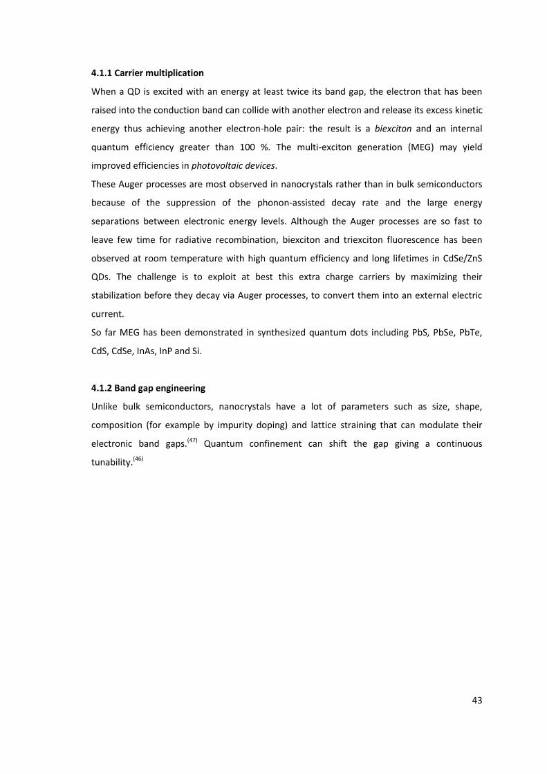
4.1.1 Carrier multiplication
When a QD is excited with an energy at least twice its band gap, the electron that has been
raised into the conduction band can collide with another electron and release its excess kinetic
energy thus achieving another electron-hole pair: the result is a biexciton and an internal
quantum efficiency greater than 100 %. The multi-exciton generation (MEG) may yield
improved efficiencies in photovoltaic devices.
These Auger processes are most observed in nanocrystals rather than in bulk semiconductors
because of the suppression of the phonon-assisted decay rate and the large energy
separations between electronic energy levels. Although the Auger processes are so fast to
leave few time for radiative recombination, biexciton and triexciton fluorescence has been
observed at room temperature with high quantum efficiency and long lifetimes in CdSe/ZnS
QDs. The challenge is to exploit at best this extra charge carriers by maximizing their
stabilization before they decay via Auger processes, to convert them into an external electric
current.
So far MEG has been demonstrated in synthesized quantum dots including PbS, PbSe, PbTe,
CdS, CdSe, InAs, InP and Si.
4.1.2 Band gap engineering
Unlike bulk semiconductors, nanocrystals have a lot of parameters such as size, shape,
composition (for example by impurity doping) and lattice straining that can modulate their
electronic band gaps.(47) Quantum confinement can shift the gap giving a continuous
tunability.(46)
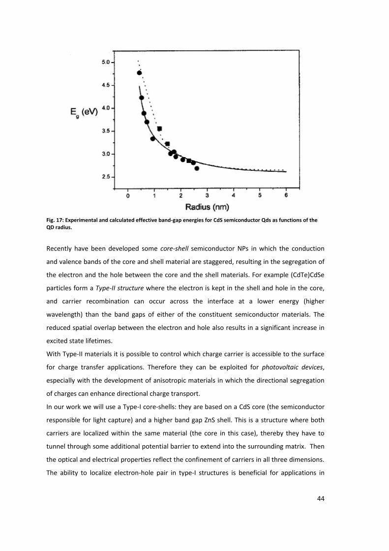
44
Fig. 17: Experimental and calculated effective band-gap energies for CdS semiconductor Qds as functions of the QD radius.
Recently have been developed some core-shell semiconductor NPs in which the conduction
and valence bands of the core and shell material are staggered, resulting in the segregation of
the electron and the hole between the core and the shell materials. For example (CdTe)CdSe
particles form a Type-II structure where the electron is kept in the shell and hole in the core,
and carrier recombination can occur across the interface at a lower energy (higher
wavelength) than the band gaps of either of the constituent semiconductor materials. The
reduced spatial overlap between the electron and hole also results in a significant increase in
excited state lifetimes.
With Type-II materials it is possible to control which charge carrier is accessible to the surface
for charge transfer applications. Therefore they can be exploited for photovoltaic devices,
especially with the development of anisotropic materials in which the directional segregation
of charges can enhance directional charge transport.
In our work we will use a Type-I core-shells: they are based on a CdS core (the semiconductor
responsible for light capture) and a higher band gap ZnS shell. This is a structure where both
carriers are localized within the same material (the core in this case), thereby they have to
tunnel through some additional potential barrier to extend into the surrounding matrix. Then
the optical and electrical properties reflect the confinement of carriers in all three dimensions.
The ability to localize electron-hole pair in type-I structures is beneficial for applications in

45
which high PL and chemical stability is required (we will have exactly the above mentioned
problems).
4.2 Synthesis methods
Synthesis of semiconducting QDs made of two different elements (usually belonging to II-VI
groups or III-V) involve the reaction between two solutions which contain the respective
elements that are going to constitute the crystal lattice of the desired semiconductor.
Among nanometric semiconductors, CdS NCs have attracted much attention due to their size-
dependent photoluminescence (PL) tunable across the Visible spectrum, and to the advances
in their preparation method that make them suitable for solar energy applications.
We are pretty interested in calchogenic elements semiconductors and chiefly CdS and ZnS
quantum dots.
By means of nanocrystals growth within nanocavities it is difficult to get monodispersity.
Otherwise NPs dimensions can be controlled by affecting kinetic parameters, thus hindering
nucleation and growth by varying reaction conditions and monodispersity is achieved.
Numerous colloidal (solution) chemistry methods have been developed for the preparation of
nanocrystals. The solution chemistry synthesis utilizes organic stabilizers to cap surface atoms
of nanoparticles in order to control the growth process; the kind of stabilizer is of great
importance since it affects the chemical and the physical properties of the NCs. We can
distinguish between two principal routes:
organic routes
aqueous ways: recently developed; these are more reproducible, low-cost and
environmentally friendly than organic routes and the “as-produced” samples are more
water-soluble.
We concentrate our attention on the organic routes. The most known methods are:
Use of organometallic precursors in coordinating solvents
Use of non-organometallic precursors in non-coordinating solvents
The difference between these two approaches resides in the possibility for monomers
reactivity in non-coordinating solvents to be controlled by varying the concentration of ligands
in the solvent.
Whatever the method is, the QDs surface plays an essential role. It is composed of unsatured
bonds that is empty orbitals of calcogenic (Se, S, etc.) and metallic (Cd, Zn, etc.) elements,
passivated by organic ligands. The nature of the ligands sets the solubility properties, which
are in fact dependent on the chemical environment present around the surface. The functional

46
group of the ligand choice is accomplished with regards to the nucleation and growth
conditions required. The conditions of solubility can be controlled by means of two different
methods: the direct exchange of ligands which bind more or less strongly to the surface, or the
use of a shell-micelle which doesn’t attach the particle surface and doesn’t depend on
functional groups.
4.2.1 Polyol synthesis of nanoscale MS particles (M = Zn, Cd)
To perform our synthesis we have chosen the polyol process. It involves a metal precursor that
is heated in a high-boiling alcohol (b.p > 200 °C). In the case of noble metals cations are
reduced by the alcohol to form particles of the metallic element; in contrast, while adding a
defined amount of water, non-noble metals precipitate to yield nanoscale oxide particles.
Owing to the high temperature during the synthesis, normally well-crystallized materials are
realized. As a further advantage, the polyol medium efficiently complexes the surface of the
particles; consequently, the particle growth is limited and an agglomeration of particles is
prevented.
The particle diameter depends on experimental conditions: concentration of precursors,
temperature, heating time as well as on the solubility of the NPs obtained. The size distribution
is closely related to the average particle diameter: the larger the particle diameter, the
broader the particle size distribution.

47
5. Carbon nanotubes and QDs in photovoltaics
Because of the interesting electrical properties of CNTs lots of efforts have been made to use
them in photovoltaic applications as charge (electrons) carriers.
Otherwise QDs have shown extraordinary light-harvesting abilities. They have been used in
solar cells in composites with polymers with quantum yields less than 2 %. This percentage is
relatively low in comparison to inorganic solar cells. This disadvantage is mainly due to the
difficulties in transferring the charge carriers away from QDs in the device.
Use of CNTs can be a solution: they can “electronically communicate” with NPs. CNTs
decorated by QDs could act as nanowires that promote direct charge transport and efficient
charge transfer to QDs, thus creating efficient solar cells.
Our experience will revolve around these concepts.
5.1 Solar cells based on NPs
In solar cells based on NPs the photoexcitation of the QDs results in the formation of an
electron-hole pair in the conduction band and the valence band respectively. The ejection of
the conduction-band electrons to the electrode, with concomitant scavenging of the valence-
band holes by a solution-solubilized electron-donor, results in the formation of an anodic
photocurrent.(48) Alternatively, the trapping of the conduction-band electrons by an electron-
acceptor, solubilized in the electrolyte solution, and the subsequent transfer of electrons from
the electrode to the valence-band holes yield a cathodic photocurrent. The electron-hole
recombination in the NPs is, however, a rapid process that competes with the electron-
ejection process, to the electrode or to the acceptor trap, and this results in a low light-to-
electrical energy conversion efficiency. Thereby many efforts have been done to improve the
efficiencies of solar cells by delaying the electron-hole recombination. Among these we can
consider the use of composite semiconductor nanoparticle structures, such as CdSe/TiO2,
CdS/SnO2 (20),(33), or core-shell semiconductor NPs as means to enhance charge separation, and
still the incorporation of semiconductor NPs in organic semiconductor polymer matrices.
Finally we concentrate on the methods that involve the creation of an hybrid structure
between semiconductor NPs and functionalized carbon nanotubes.
Before talking about our functionalization strategies we report some studies on the use of
CNTs and QDs for opto-electronic devices.

48
5.2 CNTs in OPVs
Organic photovoltaic cells operate in a different way compared to P-N junction devices. They
don’t capitalize on electric field of a P-N junction to separate the electrons and holes created
when photons are absorbed. When a photon is converted into an electron-hole pair, typically
in the donor material, the charges tend to remain bound in the form of an exciton, and are
separated when the exciton diffuses to the donor-acceptor interface. The short exciton
diffusion lengths of most polymer systems tend to limit the efficiency of such devices.
Combining the physical and chemical characteristics of conjugated polymers with the high
conductivity along the tube axis of CNTs is an interesting idea to improve efficiency of OPV
devices.
5.3 CNTs in DSSCs
In DSSCs TiO2 nanoparticles have been widely used as a working electrode because they
provide a high efficiency, more than any other metal oxide semiconductor investigated.
Despite the success of this cells the effort to further enhance efficiency has not produced any
major result. The transport of electrons across the particle network has been detected as a key
problem in achieving higher photoconversion efficiency. Because of many grain boundaries on
the electrons random path the probability of their recombination with oxidized sensitizers,
before they are efficiently collected at the electrode surface, is increased. This results in
inconvenient enlarging of oxide electrode surface area.
Therefore semiconducting CNTs electron-accepting ability could be used to direct the flow of
photogenerated electrons and assist in charge injection and extraction. To assist the electron
transport to the collecting electrode surface in a DSSC, CNTs can be used as anchor light
harvesting semiconductor particles.(33) On the other hand the organization of photoactive
donor-acceptor assemblies on the electrode surface has already shown to offer significant
enhancement in the photoconversion efficiency of solar cells.(35)

49
Fig. 18: photovoltaic device based on CNT-TiO2 hybrids (33)
The analysis performed on CNT/DSSCs has highlighted no significant influence in the charge
injection rate by the presence of SWCNTs in the film. However the photoinjected electrons in
TiO2 survive roughly 50 % longer when embedded within the SWCNT network. The
equilibration of electrons between SWCNT and TiO2 results in the transfer of a fraction of
electrons into SWCNT, thus stabilizing the photogenerated electrons and reducing the rate of
exciton recombination. Moreover, suppressing the back electron transfer and improving the
electron transport within the nanostructured TiO2 film are regarded as the two most important
factors controlling the overall IPCE of the cell: in fact photoconversion efficiencies are
generally enhanced.

50
Fig. 19: influence of CNTs in DSSCs (33)
Furthermore, some researches indicate that introducing CNTs decreases the TiO2 crystalline
grain and particle size: thus TiO2 semiconductor may possess a larger surface area and have a
greater number of contact points among the particles, CNTs and the substrate. These results
are beneficial for the improvement of the cell performance.
In few words, CNTs facilitate charge separation and promote electron transport to the
electrode surface, thus generating higher photocurrent at the expense of the open-circuit
voltage. Unfortunately any improvement in photocurrent is nullified by the increase in
photovoltage. But this is the result of a multiple separated deposition of semiconducting CNTs
followed by a TiO2 film onto an electrode.
Other essays have been done with a CNT dispersion of MWCNTs in TiO2 through a modified
acid-catalyzed sol-gel procedure from alkoxide precursors that prevents the aggregation of
MWCNTs.(34) Here the CNT loading is quite low (0,1-0,5 % in weight) and the overall behavior of
the cell depends on it. It was observed that the efficiency value was enhanced effectively with
the increase of MWCNT loading (until a certain percentage) owing to higher IPCE values,
photocurrents and this time also higher open-circuit voltages. However with a higher MWCNT
loading the Isc values exhibit a considerable decrease as the MWCNT content increases. This
may be due to the light harvesting competition between the dye-sensitizer and the MWNTs
(it’s always the case of the presence of semiconducting CNTs).

51
5.4 Combination of CNTs and conductive polymers
Use of polyanilines, polypyrroles and polythiophenes has been investigated to combine
conductive electroactive polymers and CNTs into composites with unprecedented mechanical
and electrical properties. Different preparation methods are currently in use to get the best
interaction between the two materials. For example composites prepared by in-situ
polymerization of aniline in the presence of MWCNTs enhance electronic properties,
attributed to interactions between the Pan-quinoid unit and the MWCNT surface: during
polymerization CNTs are thought to guide the growth of aniline acting as molecular templates,
facilitating efficient π-π interactions between Pan and CNT. It can be expected that composites
based on “metallic polyaniline” and individual CNTs should be able to push conductivity values
toward and possibly beyond 104 S/cm depending on the quality of CNTs, the state of CNTs
debundling and interactions between Pan and CNTs.
5.5 Decorating CNTs with metal or semiconductor NPs
Due to their large chemically active surface and stability at high temperatures CNTs have been
used as a support material for linkage of metal and semiconductor NPs. Several ways have
been investigated to immobilize NPs on the CNTs surface:
formation and stabilization (reduction and deposition, in-situ) of metal NPs directly on
CNTs surface
connection of chemically modified NPs to CNTs or to modified CNTs using covalent
linking through organic fragments or weaker bonds (the linker simply sticks to the CNT
surface through weak intermolecular interactions such as stacking, hydrophobic
or electrostatic attractions).
The most important issue for the development of these hybrid materials for technological
applications is related to discovery of powerful synthetic strategies to create materials with
reproducible properties and performances. Each approach possesses some advantages and
drawbacks. It is the potential application that determines which one is preferable each time.
The direct reduction-deposition method is simple and effective, it allows to deposit a
large amount of NPs; on the contrary it is difficult to control NPs characteristics such as
size, shape and composition
Chemical linking processes are more complicated and often based on a multistep
reaction (formation of NP, chemical modification of both components and their
connection); moreover the number of NPs linked to CNT depend on the number of –
COOH or other functional groups present on the nanotube thus it is limited; otherwise

52
NPs, which are formed separately previously, can be selected by size or shape and the
connection can be reversible.
Generally approaches relied on covalent methods require breaking of C=C bond and the
reaction of the resulting –COOH group to give products via nucleophilic acyl substitution: this
alters the SWCNTs structural and electronic properties by disrupting the sp2 hybridized
bonding and the 2p-2p conjugation. Instead non-covalent strategies which use orbital
interactions mitigate this concern.
For our purpose we concentrate on chemical linking of preformed NPs. Here we present some
examples:
oxidation of SWCNTs and subsequent reaction with aliphatic amines, to give amides
leads to soluble functionalized nanotubes; then Au NPs are connected to oxidized
SWCNTs using aminothiols or bifunctional thiols which act as linkers for Au colloids; the
same strategy is also used for functionalization with thioether groups.
acetone molecules absorbed on CNTs are seen to interact hydrophobically with Au
nanoclusters covered with a monolayer of octanethiols. Besides if NPs are covered by a
mixed-monolayer of decanethiol and mercaptoundecanoic acid they can be efficiently
linked to oxidized CNTs: we have a double interaction both hydrophobic between the
alkyl chains and the CNT surface and hydrogen-bond between COOH groups of CNTs
and those present on the NPs surface; this leads to very stable composite materials
(for example, thermal treatment at 300 °C to remove the capping shells of the Au NPs
induces aggregation of the NPs that stick strongly to CNT surface, and sonication in
hydrophobic solvents fails to disassemble the composite material).
recently a predictive model for interactions (charge transfer, Van der Waals,
covalent..) between TOAB-stabilized Au NPs and covalently modified MWCNTs with
alkyl and alkylthiol chains has been reported to predict the coverage of CNTs by Au
NPs for a range of different experimental conditions. For example, arising from both
experiments and theory, it has been seen that as length of the alkyl chains at the
surface of the MWCNTs increases the coverage decreases. The understanding of the
parameters that control MWCNTs-NPs assembly are the basis for design and control of
more complex hybrid materials.
pyrene molecules, bearing a long aliphatic chain terminated by a thiol group can
connect CNTs to Au NPs via -stacking of the pyrene moiety to the CNT surface.
Spectroscopic experiments on the composite material show that the pyrene
fluorescence is completely quenched: this implies a charge transfer character between

53
CNTs and Au NPs mediated by the linker. This kind of electron transfer process has also
been observed to occur on SWCNT-Zn porphyrin hybrid materials. The approach has
been extended to other linkers with similar structures such as 1-pyrenemethylamine,
N-(1-naphthyl)ethylenediamine and phenethylamine demonstrating the generality of
this strategy.
electrostatic interactions have also been used to anchor metal NPs to CNTs. For
example oxidized CNTs have been treated with a ionic polyelectrolyte which serves as
an anchor for charged metal NPs. By choosing different kinds of polyelectrolytes
(cationic or anionic) the surface of the CNT can be positively (negatively) charged in
order to accept negatively (positively) charged NPs.
CdSe has been connected to CNTs. QDs are stabilized with a mixed-monolayer of
trioctylphosphine oxide and 2-aminoethanethiol. The amino-functionalized QDs react
with the carboxylic groups of the oxidized SWCNTs, forming amine bonds. A significant
charge transfer is observed.
heterojunctions between MWCNTs and thiol-stabilized ZnS-capped CdSe QDs have
been created. The same strategy was used to attach CdS QDs to CNTs and this allows
to reach an efficiency up to 70 %, higher with shorter CNTs. The result suggests that
the length of CNT plays a major role in the formation of photocurrents and probably
the defects in the CNTs affect the extent of charge separation that follows the
photoexcitation of the CdS NPs.
A LBL (layer-by-layer) self-assembly technique has been exploited for the deposition of
CdTe nanocrystals onto CNTs yielding linear colloidal CNT@CdTe composites with a
high degree of coverage. The photoluminescence quenching of the QDs can be
controlled through the growth of a silica-shell spacer between the CNT surface and the
deposited QDs: the SiO2 layer minimizes the photoluminescence quenching and
preserves the quantum confinement effects.
a 1-pyrenebutyric acid N-succinimide ester (PBASE) molecule has been used for the
non-covalent functionalization of SWCNTs (both metallic and semiconducting), then
attached to 4-aminothiophenol functionalized NPs. The effectiveness of the
interaction between PBASE and CNT is highlighted by absortion spectra analysis;
in fact in the SWCNT@PBASE spectrum we can notice a red-shift for the second
SWCNT semiconducting transition (E22) and first metallic transition (E11): these red-
shifts imply interactions which promote delocalization of electrons in the

54
SWCNT thereby lowering the absortion energy associated with the interband
electronic transitions. These results are consistent with shifts observed in Raman
spectroscopy analysis: peaks frequency slightly changes in SWCNT@CdSe (congruent
with red-shifts) but none of the major Raman modes are disrupted by the non-
covalent interaction with PBASE or attachment of CdSe QDs.
5.6 Our strategies
The focus of our work will be the creation of MWCNTs@QDs composites using CdS and
CdS/ZnS core-shells as semiconductors and exploiting their sulfur-affinity to embed them into
CNTs by means of different functional groups. Among these linkers we aim to test a
mercaptosilane, mercaptobenzene and a carbamate compound.
Therefore here we will show the characteristics of these ligands and their use in applications
we can take advantage of.
5.6.1 Ligands characteristics
Phosphines, amines and thiols are groups able to strongly adhere to the surface of the QDs.
Thiols exhibit the strongest affinity thus being the most used, but they can be easily photo-
oxidized on the surface of the QDs, which can cause aggregation of the QDs. Carbodithioate
ligands are much more stable against photo-oxidation and thus would be a better choice for
protecting the QDs, however their flexibility is limited. Dithiocarbamates instead are highly
photostable as well as easy to synthesize.
Therefore to embed QDs in CNTs a double strategy can be followed by means of dithiol-
functions: CNTs can be functionalized and later the affinity of cations of NPs for Sulfur can be
exploited; otherwise QDs can be directly functionalized with ligands with a double function
which allows them to interact both with NPs and aqueous/organic solvents. Generally most of
the organic synthesis lead to QDs coated with hydrophobic molecules. Two main strategies
exist for converting hydrophobic QDs into hydrophilic ones: the former involves the use of
some amphiphilic micelles hosting internally QDs, the latter consist of exchanging of the
original organic layer with hydrophilic ligands.
The advantages of a process using dithiocarbamate moieties, for example, are the easy
reaction setup: it consists in simply mixing the amines with carbon disulfide (CS2) in the
presence of a base. Depending on the intrinsic nature of the substituents borne by the amino
group, different properties are conferred to the compound, such as solubility in various
solvents (if the amine has a carboxylic group we obtain solubility in water etc.).

55
Examples
Dithiocarbamates have been used to decorate PbSe nanocrystals with fullerenes. This
compound C[60]-PbSe shows potential applications in solar energy conversion.
Dithiocarbamate is suitable for the ligand exchange reaction of nanoparticles due to its
strong coordination ability to metal ions. However a drawback has to be taken into
account: such kind of ligand is stable only in its salt form (basic conditions), so its
solubility in common organic solvents is quite low. To solve this problem a small-
molecular-weight co-ligand with a long ethylene glycol chain has been used, to ensure
solubility of the C[60]-PbSe in both polar and non-polar solvents.
MWCNTs have been functionalized with mercaptobenzene moieties and gold
nanoparticles have been self-assembled onto their surface. It has been demonstrated
that aryl-diazonium salts react efficiently with individual CNTs via sidewall covalent
modification, and thiol derivatives interact strongly with noble nanoparticles.
Mercaptobenzene has an aryl nature: delocalization of electrons in benzene ring
facilitates electron tunneling and hence reduces electrical resistance between Au and
MWCNTs.

56
6. Absorption and photoluminescence spectroscopy
As mentioned in the fourth chapter bulk semiconductors have a fixed band gap and a
continuous conduction band, so the absorption spectrum presents a sharp increase in
correspondence of the energy gap and a quite constant absorption for higher energies.
Fig. 20: absorption spectra of bulk semiconductors and quantum dots
Instead for quantum dots the spectrum involves the presence of a first peak (the 1s(e)-1s
transition) and a non-constantly increasing absorption at shorter wavelengths, sometimes
showing other more or less definite peaks or shoulders in correspondence of higher levels
transitions (1p(e)-1p, etc.).
6.1 Absorption and photoluminescence of CNTs
Absorption and photoluminescence properties of CNTs depend on various conditions: first of
all we have to remark that most of knowledge about the properties of CNTs concerns single-
wall carbon nanotubes and really poor literature is found about multi-walled CNTs; besides the
semiconducting or metallic nature of CNTs has to be taken into account: normally different
manufacturing processes give different size and helical distributions of SWNTs composition
(typically up to 50 SWNT species are believed to be contained in HiPCO (high-pressure carbon
monoxide method) samples); afterwards a main role is played by the dispersion conditions of

57
the nanotubes in respective solutions (mono-dispersion or CNTs bundles). Eventually the
diameter of SWNTs influences the optic characteristics because of the modulation of the band-
gap.(44)
Fig. 21: Representation of the photoluminescence absorption and emission sequence in semiconducting SWNTs
Absorption spectra of SWNTs bundles contain three broad absorption regions corresponding
to the first and the second allowed transitions for semiconducting SWNTs, and the first
allowed transitions for metallic SWNTs, respectively.(45) However, these spectra do not exhibit
any features identified with a particular nanotube structure, since strong electronic coupling
mixes the energy states from the different SWNTs in the bundle. This strong intertube
coupling, combined with the large inhomogeneity in nanotube structures present in an
ensemble, completely obscures any fine structure in the absorption spectra.

58
Fig. 22: Absorption spectrum of SWNTs. The peaks at 1700 and 950 nm are due to semiconducting
NTs, the peak at 650 nm to metallic NTs.
Isolation of individual nanotubes is critical for decoupling the optical response of one
nanotube from another. Absorption spectra of an ensemble of isolated SWNTs show many
more highly resolved features than the corresponding absorption spectrum from nanotube
bundles. These distinct features correspond to dipole-allowed optical transitions from SWNTs
with different (n,m) values and/or from higher interband transitions for a nanotube with a
given (n,m) value.
6.2 Luminescence principle
We call luminescence the emission of an electromagnetic radiation which is not of thermal
origin. It is a process in which an atom/molecule absorbs photons (e.m radiation) and is
consequently excited to a higher energy state. Following this, electrons go to populate more
energetic levels, leaving some correspondent holes in the valence band they have abandoned.
Electronic transitions occur in 10-15 s, that is an instantaneous time compared with the time
scale of nuclear motion (Franck-Condon principle).
The electrons with a higher energy are unstable and tend to come back to the less energetic
state, thus recombinating with the hole. Disexcitation can occur in different ways:
Radiative pathways: fluorescence and phosphorescence
Non-radiative pathways: vibrational relaxation, energy transfer to other molecules or
to the solvent

59
For what concerns radiative pathways, it can happen that:
a photon with λemiss = λexcit is emitted (resonance transition)
different photons with λemiss > λexcit are emitted, so passing through intermediate
levels (S1) (Stokes shift)
following collision with other atoms, the excited atom can be taken to an energy level
where disexcitation is unlikely (T1): atoms can spend a lot of time in this state, before
other collisions lead them to the lower energy state (Phosphorescence).
Fig. 23: Energetic levels in a molecule of fluorophore
During an electronic transition a change from one vibrational energy level to another will be
more likely to happen if the two vibrational wave functions overlap more significantly (fig. 24).
We concentrate our attention on photoluminescence of semiconductors, particularly of small
dimensions, i.e. quantum dots. Quantum dots are semiconductor clusters of few hundreds of
atoms characterized by a gap between the HOMO and LUMO energy levels, as previously
mentioned. According to the Morse potential, at each electronic state are associated some
vibrational (and rotational) excited states. At room temperature energy is not enough to let
electrons populate excited energy states (S1, S2 etc.); thus we must make use of
electromagnetic radiation rather than heat to induce fluorescence.
In photoluminescence analysis a monochromatic radiation is used (wavelength sufficiently low
to cross the gap). The fluorophore is usually excited to some higher vibrational levels of either
S1 or S2. With few exceptions, the excess energy is rapidly dissipated, in fact molecules quickly
relax to the lowest vibrational level (Kasha’s rule) of S1 (internal conversion, which lasts 10-12 s

60
or even less) and from there can decay to the lowest electronic state via photon emission
(Fig.23).
Since fluorescence lifetimes are longer (10-8 s) internal conversion occurs before emission takes
place. Hence fluorescence emission generally results from a thermally equilibrated excited
state, that is, the lowest energy vibrational state of S1. Return to the ground state typically
occurs to a higher excited vibrational ground state level, which then quickly (10-12 s) reaches
thermal equilibrium.
Fig. 24: Franck-Condon principle energy diagram (left), and schematic representation of the
corresponding absorption and fluorescence spectra (right)
An interesting consequence of emission to higher vibrational ground states is that the
emission spectrum is typically a mirror image of the absorption spectrum of the S0-S1
transition. This similarity occurs because electronic excitation does not alter the nuclear
geometry (the spacing of the vibrational energy levels of the excited states is similar to that of
the ground state). So emission spectra are typically independent of the excitation wavelength.
Typical PL spectra of quantum dots show a peak correspondent to the emission from the
LUMO level (excited state) to a vibrational state of the HOMO (ground state), then resulting in
a little red-shifted peak respect to the absorption one (fig.25).

61
Fig. 25: PL peak shift respect to absorption spectrum
Due to the presence of some defects , thus to some energy states available inside the band
gap, radiative transitions involving higher wavelength photons emission are possible; for the
same reason an assessment of their concentration can be obtained.
Fluorescence lifetime and quantum yield are the most important characteristics of a
fluorophore.
Quantum yield (QY) is the number of emitted photons relative to the number of absorbed
photons. Substances with the largest QY, approaching unity such as rhodamines, display the
brightest emissions. Non-radiative decays affect both the excited state lifetime and the QY; the

62
more frequent include: dynamic collisional quenching, near-field dipole-dipole interaction
(fluorescence resonance energy transfer, FRET), internal conversion and intersystem crossing.
Fluorescence quantum yield is measured by comparison with a standard with known QY. It
doesn’t depend on the excitation wavelength.
Fluorescence lifetime of the excited state refers to the average time the molecule spends in
the excited state prior to return to the ground state. It typically follows first-order kinetics:
where S1 is the concentration of excited state molecules at time t, S10 is the initial
concentration and Γ is the decay rate or the inverse of the fluorescence lifetime. If different
radiative (Γrad) and non-radiative (Γnrad) processes contribute to depopulate the excited state,
the total decay (Γtot) will be the sum of the two terms: Γtot = Γrad + Γnrad
Generally fluorescence lifetimes range from 0,5 to 20 ns.
6.2.1 Luminophores
Among the most known luminophores we can remind the organic dyes with unsatured bonds
(benzene and derivatives), inorganic crystalline substances (ZnO, ZnSe, CdS, CdTe, GaAs, InP ..),
doped silicates and oxides, inorganic liquid or amorphous substances (UO2, Neodymium
glass,..).
The majority of organic fluorophores are not photostable and display photobleaching with high
illumination intensities. There are different types of luminophores that are mostly inorganic or
display unusually long lifetimes (semiconducting NPs, lanthanides and transition metal-ligand
complexes (MLCs)).
Quantum dots allow to obtain a wide range of emission wavelengths by simply changing the
size or chemical composition of the NPs: it has been extended to 4 μm using PbSe particles
(PbSe QDs with emission λ near 2 μm display QY as high as 25 %).
Chemical and photochemical stability are improved by coating the QD core with a material
with a higher band gap (core-shell quantum dots), which confines the excited state to the
center of the particle, thus preventing interaction with the surface.
QDs display several favorable spectral features. The emission spectra of homogeneously sized
QDs are about twofold more narrow than typical fluorophores. QDs don’t display the long
wavelength tail common to all fluorophores.
QDs also have large extinction coefficients (ε) that on a molar basis can be up to tenfold larger
than rhodamine.

63
6.2.2 Fluorescence of CNTs
SWNTs are poor emitters: the fluorescence QY of SWNTs is on the order of about 10-4. Metallic
SWNTs with continuous valence and conductance bands display little or no PL.
Early optical studies could only determine an average overall behavior that obscures crucial
electronic characteristics of the individual nanotubes. For example, since spectra from SWNTs
with different (n,m) values will overlap, it is difficult to make definite conclusions regarding
important emission features such as the spectral line width or details of the band shape, or to
observe evidence of coupling to vibrations.
Interaction between nanotubes or between nanotube and another material (substrate)
quenches PL. For this reason, no PL is observed in MWNTs.
For the same reason bundled SWNTs do not fluoresce since any metallic tube present in the
bundle provides an efficient non-radiative pathway for photoexcited electrons.
The situation could be different whether CNTs are functionalized with some
aromatic/conjugated compounds with orbitals which absorb light. For example for MWNTs
with in-situ polymerized thiophene (PTh) there is an intense emission at about 430 nm which
can be attributed to the emission of polythiophene. (17)
6.2.3 Quenching
The intensity of fluorescence can be decreased by a wide variety of processes. Such intensity
reduction is the result of some disexcitation processes due to charge or energy transfer from
excited states. These processes are known as Quenching.
It can be dynamic or static. So if we talk about luminophores in solution it’s possible that some
particular molecules called quenchers diffuse, collide and interact with fluorophores
disexcitating them (implying a transfer of charge/energy): the presence of the quencher adds
another deactivation pathway in competition with luminescence (dynamic quenching).
Otherwise if the luminophore is somehow associated with the quencher prior to light
absorption another kind of transfer can take place: static quenching. The reduction in emission
intensity will be affected by the extent to which the quencher associates to the luminophore
and the number of quenchers present.
As shown in recent works by many authors, CNTs can well play the role of effective quenchers.
When QDs are grafted to functionalized CNTs, an efficient transfer of charge generally occurs.
There are some possible explanations for the PL-band quenching (11): electron transfer, hole
transfer or both into the MWNTs, or resonant energy transfer (14) ,(18).

64
PL spectra of QDs generally show a strong emission peak in correspondence of band-edge
electron hole recombination along with some peaks at higher wavelength which can appear
following trap emission. This signal is partially quenched in the simple mixture of CNT and QDs
and totally quenched in the nanohybrids. Thus the reduction of the main peak can be assigned
to the charge/energy transfer from CNTs to QDs. In CNT-QDs systems electron-hole
recombination competes with an electron injection mechanism, and this competition depends
on the distance between the CNTs and QDs. So for the CNT/QDs mixtures just part of the
electrons is transferred to the CNTs, while the remainder of them produces a reduced
emission through radiative relaxation. In contrast when the QDs are well linked to the CNTs by
means of some functionalities, the emission is totally quenched, because electron injection
from the QDs to the CNTs dominates. (17)
Moreover red-shifts in the peak position can be seen for CNT@QDs nanohybrids respect to the
lonely QDs (19), suggesting that strong electronic interaction of QDs with CNT occurs after
photoexcitation of the hybrid material.
On the other hand MWNT can have a weak absorption band located near the emission peak of
QDs (12), so that energy transfer from QDs to MWNT might also contribute to the quenching
mechanism, thus decreasing the electron transfer efficiency.
6.2.4 CNTs/QDs distance
Some studies about distance issue have been accomplished. For example different capping
agents with various chain lengths have been used to wrap QDs subsequently attached to CNTs
(the separation between the QDs and the CNTs is adjusted by the lengths of alkyl chains of the
capping agents). (15) The PL spectra show that the intensity of the QD emission peaks in the
QD@CNT hybrid is strongly dominated by the shell thickness, that is the PL brightness
increases with the chain length of the capping agent (mercapto-carboxylic acid in this studied
case) on the QDs. It has been seen that as the average distance between the QDs and CNTs
increases within 10 Å ranges, the photoluminescence properties of the nanohybrids change
from total quenching to nearly no quenching. These studies consider charge transfer through
alkyl chains, so maybe thanks to electro-tunneling. Perhaps it is different with conductive
and/or aromatic interlinkers.
6.2.5 CNT direct linking
The properties of a monolayer of CdS NPs assembled on a Au electrode by covalent coupling
have been compared to that of a CdS/CNT system and the results show that, despite the same

65
surface coverage of NPs, both the photocurrent generated by the systems that lacks the CNT
connectors and the photon-to-electron quantum efficiency are substantially lower. This means
that CNTs which bridge the CdS NPs to the electrode play a major role in the enhanced
generation of photocurrents. (27)
6.2.6 CNT length
We know that the longer time intervals of acidic digestion yields shorter tubes. Then CNTs of
different lengths (different digestion times) have been used to assemble CNT/CdS NPs-
functionalized electrodes. The photocurrent obtained reveal that it is enhanced as the
digestion time of the CNTs is increases (shorter linking CNTs). The quantum efficiencies
increase as the digestion time increases (shorter CNTs) as well (31). Some hypothesis can
support this behavior. The conductive CNTs provide efficient paths for the transport to the
electrode of the trapped conduction-band electrons originated in the NPs, and the charge-
transport rates in CNTs should be almost length-independent. But we have to consider that the
oxidative acidic digestion of the CNTs not only shortens the CNTs but it also introduces defects
into the sidewalls. So according to a back-scattering model, as the electron reaches a defect
site, it is back-scattered to find an alternative conjugated path to be transported along the
CNT. As the number of defects in the CNT increases with its length, charge transport along the
CNT could be dominated by its length. As the CNTs become longer, more defects exist in the
connecting wires and thus the back-scattering process retards the conductance of the trapped
electrons to the electrode; so they can recombine with the valence-band holes to result in
lower quantum yields for the photon-to-electron conversion process.(27)

66
6.2.7 Energetic levels position
Fig. 26: Schematic energetic band position for MWNT and some semiconductors
The non-radiative decay path occurs because the difference in electron affinity between the
QDs and the CNTs is sufficient to allow electron transfer from the QDs to the CNTs.
The conduction energy level of CNTs (about -4,5/-5 eV against vacuum) resides normally inside
the band gap of the quantum dots, so that to scavenge electrons from the conduction band of
the last ones, preventing exciton recombination thus decreasing (or cancelling) luminescence
intensity.
Fig. 27: Energy level diagram and possible charge-transfer process for the conjugate complex between
CdSe QDs and semiconducting NTs (s-CNT) or metallic NTs (m-CNT)

67
The conduction and valence band levels for both QDs and SWNTs depend on their diameter. (14)
For instance, since the effective mass of a hole (1,19 me, where me is the electron mass) in
CdSe is much larger than the effective mass of an electron (0,11 me), the valence energy in
CdSe QDs does not change, while the conduction energy changes noticeably.
In MWNTs the presence of numerous concentric graphene cylinders provides different
acceptor levels (19).
The absolute and relative position of the Fermi levels of the components of the photovoltaic
device are fundamental for the solar cell efficiency.
The Fermi level equilibration between the sensitizer and the CNTs often drives the open circuit
voltage lower than the one obtained with the sensitizer and TiO2 films (that is the case of
DSSCs). (20) Thus despite the success in the fast capture of electrons from the QD to the CNT,
the lower energy difference (and hence the open circuit potential) limits the overall
photoelectrochemical performance of these solar cells. Further modifications of CNTs with
semiconducting composites and/or functional groups are necessary to drive the Fermi level to
more negative potentials.
Fig. 28: DSSCs scheme with indication of the “Open circuit voltage” (Voc): grossly it can be determined
by the energy difference between the Fermi level of the solid under illumination and the Nernst
potential of the redox couple in the electrolyte (difference between the conduction band of TiO2 and
the redox couple for DSSCs; difference between the CNT Fermi energy level and the redox couple for
these kind of photovoltaic devices)

68
The efficiency of charge transfer is determined not only by the energy difference between
donor (QD) and acceptor (CNT), but also by the exciton binding energy of the QDs. (14) The
donor-acceptor energy difference should be greater than the exciton binding energy of the
QD. That is relatively large in a quantum-confined system (over 0,1 eV for CdSe QDs).
6.2.8 Core-shells
We have to pay attention to the case of core-shell QDs attached to CNTs.
For example when CdSe/CdS core-shell particles (Type-I structures) are attached to MWNTs,
the PL is completely quenched. Instead the PL of CdSe/ZnS core-shells (type-I) decreases
slightly upon association with SWNTs. (14)
Fig. 29: Photo-induced charge-transfer between core-shell QDs and CNT@diazo-SH. The transfer is
controlled by the shell thickness
In fact it has been observed that if the shell coating is not sufficiently thick charge carriers may
leak from the core. Therefore CdS NPs, which have a smaller band gap (respect to ZnS) and a
smaller conduction band offset with CdSe (about 0,32 eV) are more susceptible to PL
quenching. On the contrary ZnS has a larger band gap and may confine the exciton more
efficiently.

69
Fig. 30: enegy levels positions against vacuum of some semiconductors
Another proof has been taken from the study of MWNTs coated with silica. The large band gap
and thickness of the SiO2 rules out both charge transfer and electron tunneling as possible
quenching mechanisms. (11), (20)
6.2.9 Time-resolved spectroscopy
To probe the ultrafast electron transfer in the sub-nanosecond time scale, some researchers
have employed Femtosecond transient absorption spectroscopy.(20) The analysis points out that
the charge injection between excited QD and CNT is an ultrafast process, and it can be
modulated by controlling the particle size. An increase in the electron transfer rate constant is
observed while decreasing the particle diameter from 4,5 to 3 nm. The higher energy
conduction band in the smaller size quantum dots play a role in maximizing the electron
transfer rate to the CNTs.
In order to further prove and support electronic communication between CdS and CNT, the
photoinduced dynamics of the nanohybrid excited state were investigated by Time-resolved
spectroscopy techniques. (19)
Fluorescence lifetimes of the excited CdS in nanohybrids have been evaluated to be more than
10 times shorter than the lifetime of capped QDs, thus supporting the efficient emission
quenching of CdS by the nanotubes in the nanohybrids, as observed in the fluorescence-
intensity quenching in the steady-state spectra and the appreciable red-shift of the
fluorescence peak.
Time resolved spectroscopy has highlighted a quick recovery for the bleaching (most of which
is completed within 200 ps) in CNT@CdS hybrid systems (21); instead the CdS alone shows long-
term recovery and extends beyond 1500 ps. This indicates that an additional deactivation

70
pathway exists for the electrons in the quantum dot conduction band and this is likely another
proof of the transfer of charge carriers to the CNT.
6.2.10 Identity of carriers
The identity of the primary carrier in the QD/CNT device can be determined by measuring
various electrical signals of the QD-CNT assemblies. (14)
Generally the SWNTs are hole-transport materials (13); electron transfer from the quantum dots
to the nanotubes under illumination results in electron-hole recombination within the
nanotubes and thus a reduction of carrier concentration and also a decrease of the
photocurrent. In contrast to the SWNTs it’s very likely that functionalization (with oleylamine
in the cited experiment) induce n-doping of the SWNT, hence making the electron a major
carrier in the hybrid system (a photocurrent build-up can be seen from analysis).

71
7. Experimental objectives
We aim to prepare nanohybrids made from CNTs and QDs.
Various functionalizations of CNTs will be presented in this part:
- grafting of thiol functions through mercaptosilane (on oxidized CNTs) or diazonium
salts (on pristine CNTs)
- grafting of amine functions through an electroyte (poly-allylamine)
- grafting of dithiol functions: as no commercial product was available, the synthesis of
two molecules is here presented.
CdS quantum dots will be synthesized via a polyol method and characterized.
The properties of all the compounds will be investigated especially through TEM and XPS
analysis.
Particular emphasis will be put on photoluminescence properties of the nanohybrids.
7.1 Synthesis of a dithiocarbamate
A lot of different synthesis which aim to get some dithiocarbamate salts have been attempted.
Most of reactions that involve the simple addition of an amine to Carbon disulfide (CS2) are
conducted under harsh conditions (use of strong basic conditions, high reaction temperatures
and long reaction times) in order to obtain high yields.
It has been said that most of reactions involve the use of secondary alkyl-amines, which are
more nucleophilic than primary ones. In general primary and secondary amines can react with
electrophilic carbon systems to form C-N bonds. These bonds are strong and thus the products
of these nucleophilic additions are stable. Besides in aryl-amines the effect of an aromatic ring
delocalizes the ion pair of electrons on nitrogen into the ring, resulting in decreases basicity
and reactivity.
We have decided to try two routes, the former less reliable (very few literature (22), (23), (24)), the
latter more successful. (25), (26)
The first aims at making phenylenediamine react with carbon disulfide trying to extract the by-
product functionalized only on one side to exploit the diazonium mechanism to further
functionalize carbon nanotubes.

72
NH2 NH2 + S S
NH4
+
NH2 NH
S-
S
Fig. 31: synthesis of a dithiocarbamate from a phenylenediamine
7.1.1 Experimental route
300 mg of 1,4-phenylenediamine are dispersed in 10 ml of ammonia (38 % in water); 1,1
equivalent (0,2 ml) of carbon disulfide is added and the solution stirred overnight at 50 °C
(Tb(CS2) = 46 °C).
The solution is of a frothy pale yellow. TLC identifies the presence of at least four compounds
in our mixture. We expect that the compound that migrates the less (one-side reacted
phenylenediamine is supposed to be more polar than the two-sides reacted product)
corresponds to our desired compound which we try to draw out. First of all we would
eliminate water from the mixture (so that to perform some NMR analysis), but because of our
product polarity we cannot just draw it out without extracting part of the product too. We
want to try to transfer our product into chloroform (not soluble in water and polar enough to
catch the desired product). Just after mixing, the mixture becomes an emulsion, thus we use a
great deal of NaCl to enable precipitatation. Then we extract the phase with chloroform and
add MgSO4 to absorb the remaining water. TLC analysis seem to confirm the presence of only
one product, so the solution is filtered and dried. The obtained product weighs 41 mg net.
(perhaps part of it has remained in the aqueous phase: maybe it is quite acid, giving rise to a
zwitterion, so it is difficult to separate it).
NMR and mass spectrometry are used without success to identify the product: NMR spectra
are too confused and from mass spectrometry we don’t find any compound with the desired
molecular weight (moreover if our product is a salt, it cannot even volatilize and thus cannot
be analyzed).
Consequently synthesis conditions have been changed a little: 2 equivalent of CS2 is used and
the temperature set at 40 °C. Then the product is solubilized in acetone, left overnight to
precipitate and finally filtered. Unfortunately from further NMR and IR analysis we cannot
demonstrate the presence of our hypothesized product (from IR we don’t perceive the
presence of NH and NH2 bonds in the spectrum).
We would need some bibliographic data to ameliorate the synthesis.

73
The second attempt involves the synthesis of a dithiocarbamate starting from an
aminosiloxane (thus a primary amine) according to some recent literature. (25)
Si NH2
O
O
O
CH3
CH3
CH3
S-
S
+NaH
Si NH
O
O
O
CH3
CH3
CH3
S
S-
Fig. 32: synthesis of a dithiocarbamate from an organosilane
We know that the reaction is sensitive to the amount of both the reagents and solvent. The
protocol is the following:
to a suspension of degreased NaH (12 mmol) in dry THF (20 ml) cooled to 0 °C are added
dropwise via syringe 3-aminopropyltriethoxysilane (APTES) (10mmol) and carbon disulfide
(CS2) in a molar ratio of 1:1,5. After being stirred under vacuum at 0 °C for 0,5 hours, the
reaction is refluxed at 65 °C for 2 hours under vigorous stirring. After cooling the volatiles are
removed under reduced pressure. The crude yellow solid obtained is purified by washing with
dry diethyl ether (Et2O) and filtered. The product seems to be partially soluble in Et2O, in fact
from NMR analysis we get the same results from the compounds which pass and doesn’t pass
through the filter. So washing with Et2O seems useless. NMR results are still confused, and IR
analysis reveal that maybe the product is a little polymerized.
For further attempts concerning this synthesis maybe we have to change the solvent to wash
the obtained solid, and use degreased NaH which is more reactive, or KH or LiH as an
alternative (the last ones are stronger bases). Moreover we must remind to prevent the
contact with air throughout the synthesis procedure because water can give some hydrolysis
reactions.

74
8. CNT functionalization
8.1 MWNTs oxidation
In literature different ways to oxidize CNTs are presented, using solutions of nitric acid (HNO3),
sulfuric acid (H2SO4) and hydrogen peroxide (H2O2) in different proportions.(40) We choose a
solution of concentrated acids as H2SO4:HNO3 in a 3:1 ratio.
As far as the experiment is concerned:
200 mg of MWNTs is introduced into a 50 ml Erlenmeyer flask followed by 8 ml of HNO3 (69 %)
and 24 ml of H2SO4 (95 %). The solution is then vigorously shaken for 1 minute and sonicated
for 5 minutes. This operation is repeated twice. Later on the flask is left in the ultrasonic bath
with heating for 3 hours.
The solution is thus soon poured in another flask and about 500 ml of distillated water are
added. Afterwards it is filtrated by means of a Buchner funnel and a nitrocellulose filter with
the diameter of the pores of 200 nm (the last one has been chosen in place of a 650 nm –
nylon membrane to keep the majority of CNTs); then some washing cycles with water let take
away the acid. In the end the CNTs are dried under vacuum for at least 2 hours. We call the
sample: MWNT@COOH.
It’s important to filtrate just after oxidation as well as wash oxidized CNTs to prevent further
attach by acids: in fact CNTs in contact with acids cut continuously in more and more little
tubes.
Oxidation under slightly different conditions has been performed to compare the oxidation
degree. According to another protocol we have accomplished oxidation by means of an
equimolar solution (8M) of nitric and sulfuric acid.
So 200 mg of MWNTs is introduced into a 50 ml Erlenmeyer flask followed by 20,5 ml of HNO3
(8M) and 18 ml of H2SO4 (8M). Then the procedure is the same as before.

75
8.1.1 Synthesis with Aminobenzoic acid (diazo-COOH)
50 mg of MWNTs and 233 mg (1,7 mmol) of 4-aminobenzoic acid is added to a 50 ml flask
equipped with a stir bar. The mixture is then deoxygenated for 5 minutes. 10 ml of
isoamylnitrite is then added via an argon-purged syringe and the solution is thus heated at 60
°C for 3 hours.
The product is then purified by filtration, washed with acetone, redispersed in DCM
(dichloromethane) and sonicated for 5 minutes; thus the filtration/washing/redispersion cycle
is repeated for 3 other times.
The functionalized nanotubes (MWNT@diazo-COOH) are then dried under vacuum for 2 hours.
8.1.2 Results
TEM analysis
Fig. 33: NTC@COOH (up and down): CNTs oxidized in a sulfuric acid - nitric acid (3:1) solution

76
Fig. 34: CNT@Diazo-COOH : CNTs oxidized with aminobenzoic acid
From TEM analysis we can perceive as result of harsh acid conditions the presence of long and
short CNTs which are by the way well functionalized. For CNTs that have reacted with amino-
benzoic acid the functionalization seems deeper and the CNTs covered with thicker layers.
Fig. 35: pristine CNTs (up) and CNTs oxidized (down) with a sulfuric acid – nitric acid solution (1:1)

77
From these SEM images we can notice that there are only slight differences between pristine
MWNTs and oxidized MWNTs. We can underline the presence of some shorter CNTs and less
smooth walls.
SEM images of MWNTs oxidized by means of stronger acid conditions could reveal a higher
degree of functionalization according to the bigger amount of oxygen displayed on XPS
analysis.
XPS analysis
Pristine MWNT:
Name Start
BE
Peak
BE
End BE Height
Counts
FWHM
eV
Area (P)
CPS.eV
Area
(N)
At. %
C1s 294,1 285,1 283 13654,7 1,1 20826,9 0,2 98,3
O1s 538,4 533,5 529,4 87,6 2,5 255,1 0 1,7 ±
0,2
Oxidized MWNT (1:1):
Name Start
BE
Peak
BE
End BE Height
Counts
FWHM
eV
Area (P)
CPS.eV
Area
(N)
At. %
C1s 293,1 284,4 282,7 118561,2 1,06 175275,5 1,5 94,7
O1s 536,5 532,3 528,3 8056,1 3,23 26959,8 0,1 5,3 ±
0,5
Oxidized MWNT (3:1):
Name Start BE Peak BE End BE Height
Counts
FWHM
eV
Area (P)
CPS.eV
Area
(N)
At. %
C1s 296,6 285,0 282,6 185583,7 1,1 345784,8 3,0 85,76
O1s 540,4 533,1 528,3 46230,4 3,1 151979,4 0,5 13,65 ±
1,4
N1s 411,4 402,5 398,2 1048,6 2,5 4181,4 0,0 0,59 ±
0,1

78
MWNT@Diazo-COOH:
Name Start
BE
Peak
BE
End BE Height
Counts
FWHM
eV
Area (P)
CPS.eV
Area
(N)
At. %
C1s 295,2 284,6 282,0 151050,5 1,1 245469,8 2,1 89,2
O1s 543,9 533,2 528,3 13490,7 3,4 62195,7 0,2 8,2 ±
0,8
N1s 410,5 400,7 396,7 3764,4 2,4 12603,0 0,1 2,6 ±
0,3
From XPS analysis we can glean some information about the atomic percentage of oxygen and
nitrogen on MWNTs. We can notice that pristine MWNTs are already oxidized: almost 2 % of
oxygen is present onto CNT surface. This quantity bumps up after an oxidation treatment using
an equimolar solution of nitric and sulfuric acid but it’s only with an acid solution in the ratio
H2SO4:HNO3= 3:1 that a significant oxidation takes place: that lets us understand that we can
vary the oxidation conditions by playing on the ratio of acids used, taking into account that
harder conditions yield shorter and more damaged CNTs.
Fig. 36: XPS Carbon high resolution spectrum of CNT oxidized (3:1); the peak at about 289 eV
correspond to the group COOH
As far as nitrogen on the unmodified CNTs spectra is concerned, only a weak signal at around
400 eV is observed: it is assigned to the atmospheric nitrogen. In oxidized CNT (under harsh
conditions) we have a slight increase in this element.

79
A remarkable increment in nitrogen percentage can be seen on MWNTs modified by
diazonium salts methods: this is probably due to the presence of N=N bonds among
aminobenzoic molecules which produces a multilayer structure onto CNTs surfaces.

80
8.2 Functionalization with a mercaptosilane
8.2.1 Synthesis
10 mg of MWNT@COOH obtained from the MWNTs oxidation process is dispersed into 40 ml
of distilled toluene in a polypropylene tube and sonicated for 1 hour at room Temperature.
Then 2 ml of MPTS (3-mercaptopropyl-trimethoxysilane) is added and the solution further
sonicated for 4 hours at about 60 °C.
Subsequently the CNTs are centrifuged at 23.000 rpm for 20 minutes and undergone 4
washing cycles with ethanol absolute. In the end the majority of supernatant is taken away
with a pipette and then with the aid of an argon atmosphere and the CNTs are dried under
vacuum for 2 hours.
We call this sample MWNT@MPTS.
In this experiment we have used distilled toluene to prevent hydrolysis mechanisms that could
lead the mercaptosilane to react on itself.
Moreover the MPTS has been afterward substituted by the less reactive MPTES (3-
mercaptopropyltriethoxysilane) also to enable a better comparison with another molecule that
we have tried to synthesize (a triethoxysilane-dithiocarbamate); the resulting product is called
MWNT@MPTES.
Fig. 37: CNT functionalization with MPTES
8.2.2 Results
In some experiments we have varied the organosilane quantity and temperature to find out
the best conditions. We can see that with about 0,2 equivalent of MPTS the CNT
functionalization reaches its maximum.

81
Here we present the sulfur and silicon atomic percentages derived from XPS spectra owing to
different quantities of MPTS; CNT amount is always the same (10 mg):
MPTS (ml) S (atomic surface %) Si (atomic surface %)
0,5 (0,05 eq) 1,1 ± 0,1 2,1 ± 0,2
1 (0,1 eq) 4,5 ± 0,5 6,8 ± 0,7
2 (0,2 eq) 4,6 ± 0,5 7,1 ± 0,7
Each mercaptosilane molecule contains one atom of Sulfur and one of Silicon so these
elements should be present in the same quantities: however from XPS spectra we notice a
ratio of 1,5 between the two elements, and it is difficult to explain why it happens.
Fig. 38: XPS Sulfur high resolution spectrum of (MPTS-0,2 eq)
From Sulfur high resolution spectrum (fig.38) we can see a large peak that could correspond to
different bonds: apart from the main peak at about 164 eV (with the characteristic doublet
correspondent to the orbitals S-2p1/2 and S-2p3/2) that should match the –SH or maybe a S-S
bond, there is a percentage of oxidized sulfur at about 168 eV (-SOxH bond).
So we can hypothesize that both the reduced sulfur oxidizes to –SOxH and it is eliminated
through bond scission. On the other hand it could correspond to the S-C bond present in the
molecules.

82
Fig. 39: XPS spectrum of (MPTES-2ml)
We can also underline the difference encountered using MPTES: sulfur spectra (fig. 40) don’t
show the peak correspondent to -SOxH and S percentage is closer to Si one:
MPTES (ml) S (atomic surface %) Si (atomic surface %)
2 (0,2 eq) 6,1 ± 0,6 7,2 ± 0,7
Fig.: 40 XPS Sulfur high resolution spectrum of (MPTES-0,2 eq)
However we would establish whether MPTS and MPTES react themselves producing a certain
amount of polymerization but neither with XPS nor with IR analysis we can evaluate this (with
IR the quantity of MPTS is too less compared to toluene to allow a clear peaks analysis).

83
TEM analysis
This photos made by TEM reveal to us that CNTs are well surrounded by MPTS molecules and
perhaps its concentration is bigger in correspondence of the CNTs ends, where there should be
the biggest quantity of COOH groups to which MPTS molecules can bind.
The MPTS layers thickness is quite small (this is vital for charge transfer issues, see chapter 6)
and no significant interactions are present among the CNTs: for CNTs modified by means of
diazonium salts it will be quite different.
Later on we will further discuss this.
Fig. 41: CNT@mercaptosilane: oxidized CNTs functionalized with a mercaptosilane
Fig. 42: CNT@mercaptosilane: oxidized CNTs functionalized with a mercaptosilane

84
8.3 Coating of CNTs with PAH (Poly-allylamine hydrochloride)
A polyelectrolyte (PAH) has been used to coat the surface of pristine and oxidized CNTs.(43) A
polyelectrolyte is a polymer whose units contain an electrolyte; this group dissociates in an
aqueous solution leaving a charge on the polymer itself. In our case the group NH2 becomes
NH3+ giving life to a cationic polyelectrolyte.
Our aim consists in enrobing the nanotube with this polymer to see if the coating involves all
the CNT or chiefly the sites where a –COOH group is present.
Afterwards we would try to graft some NPs thanks to the presence and possible interaction
with the NH2 group.
8.3.1 Synthesis
Inside a volumetric flask we dissolve 1 g of PAH into 100 ml of distilled water; the solution is
poured into another tube together with 15 mg of pristine MWNTs.
We put the tube into an ultrasound bath for 3 hours. The tube is stirred overnight at 80 °C and
sonicated again for 2 hours. Afterwards we put the compound through five centrifugation
cycles at 22000 rpm for 25 minutes and redispersion in water. Finally the powder is dried
under vacuum for 6 hours.
8.3.2 Results
From XPS analysis we can get some basic information.
Pristine MWNTs are only weakly oxidized so interaction between PAH and the CNTs are
principally of electrostatic nature: the polymer is physically absorbed onto CNT surface and it’s
the protonated amine (NH3+) which interacts with CNT -orbitals. Nitrogen amount is weak
(1,16 %); from deconvolution analysis (fig. 43) we can see that it is present under two forms:
basing on area ratios we can assign the 0,3 % to the protonated amine (NH3+) and the 0,9 % to
NH2.

85
The value for NH3+ is really close to the chlorine atomic percentage (0,3 %): in fact Cl- plays the
role of counter ion.
Fig. 43: XPS high resolution spectra of Nitrogen and Chlorum of (MWNT@Pah)
With MWNT@COOH nitrogen and chlorine percentages bump up respectively to 4,5 % and 0,7
%.

86
Fig. 44: XPS spectrum of (MWNT@COOH@Pah)
From the deconvolution of nitrogen spectrum (fig.45) we can evaluate approximately the ratio
of NH3+/NH2: the protonated amine rate is about the 76 %.
Fig. 45: XPS spectra of Nitrogen and Chlorine of (MWNT@COOH@Pah)

87
The protonated amine is however in excess respect to chlorine ions (3,46 % against 0,67 %).
This could mean that there are two possible counter ions for the NH3+ : the Cl- and the COO-
ions of the oxidized CNTs.
Unlike with pristine CNTs, with oxidized CNTs we can have different types of interactions:
electrostatic, as for pristine CNTs, and the possibility of a ionic bond between COO- and NH3+
and a covalent reaction between COOH groups and the amine NH2.
This unclear results will be confirmed by TEM analysis where CNTs will appear not to be well
functionalized. However we could hypothesize the failure of the synthesis just by considering
the difficulties occurred during the centrifugation cycles.
New XPS measurements are in progress.

88
8.4 In-situ generation of diazonium salts for grafting to the surface of CNTs
The functionalization of MWNTs with diazonium salts allows to functionalize better the entire
surface of the CNT (the external surface) and to alter less its structure.(41),(42)
The process of forming diazonium compounds is called diazotization. The most important
method for the preparation of diazonium salts is treatment of aromatic amines such as aniline
with nitrous acid. Usually the nitrous acid is generated in-situ from sodium nitrite and mineral
acid. In aqueous solution diazonium salts are unstable at temperatures above +5 °C; the -N+≡N
group tends to be lost as N2. One can isolate diazonium compounds as tetrafluoroborate salts,
which are stable at room temperature. Often, diazonium compounds are not isolated and once
prepared, used immediately in further reactions. In our experiments we follow this second
route, starting the in-situ reaction between aryl-amines and isoamyl nitrite.
Fig. 46: in-situ synthesis of diazonium compounds
The in-situ produced aryl radicals are close to the surface, in the diffusion layer , so they can
react with the surface (CNTs in this case , metals or semiconductors in others) and form a
stable covalent aryl bond (C-C or different). (28), (29)
This bond forms with extremely high affinity for electrons with energies near (within a certain
E) the Fermi level, Ef of the nanotube: metallic-CNTs have a high electron density near Ef and
this results in their high reactivity over semiconducting ones. The reaction mechanism implies
a charge transfer from the CNT surface to the reactant, stabilizing the transition state. The
creation of this “defect” increases the selectivity and makes the metallic-CNTs still more
reactive over semiconducting ones because of the disrupted bond symmetry.
The reaction is composed of two steps. First the diazonium reagents quickly adsorb non-
covalently to a CNT surface empty site, forming a charge transfer complex. During the slower
second step the reactant forms a covalent bond with the CNT.

89
These two steps are normally recognizable thanks to Raman spectroscopy: after the first stage
we can notice a decrease in the tangential vibrational mode (G-peak) of the spectrum; in the
end the G-peak is restored and the D-band increases.
The aryl radical-substrate is not the only reaction that can occur. Since the radicals produced
during this process are highly reactive, they can also interact with the aryl groups already
attached to the surface, resulting in multilayer films (generally oligomers of 5,6 units are
obtained with the possible presence of N=N, C-O and other unexpected bonds). (30)
Fig. 47: possible real structure for CNT@diazo-SH compounds: aryl layers are probably oligomers
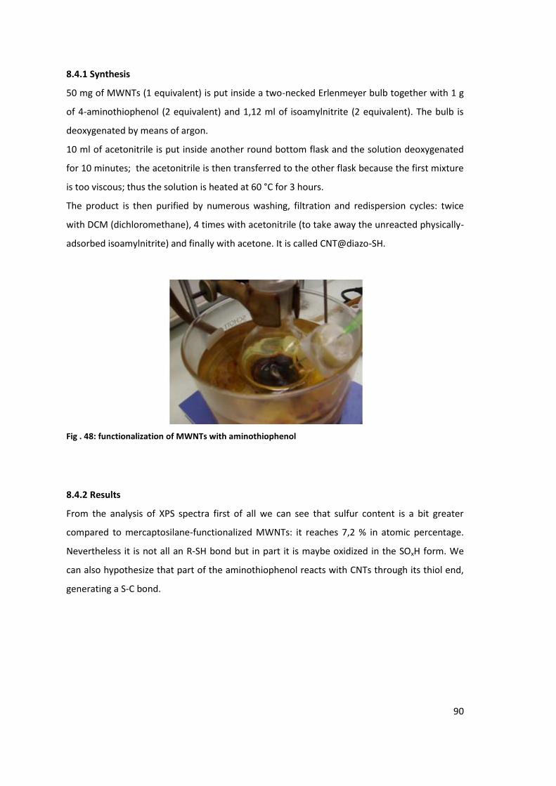
90
8.4.1 Synthesis
50 mg of MWNTs (1 equivalent) is put inside a two-necked Erlenmeyer bulb together with 1 g
of 4-aminothiophenol (2 equivalent) and 1,12 ml of isoamylnitrite (2 equivalent). The bulb is
deoxygenated by means of argon.
10 ml of acetonitrile is put inside another round bottom flask and the solution deoxygenated
for 10 minutes; the acetonitrile is then transferred to the other flask because the first mixture
is too viscous; thus the solution is heated at 60 °C for 3 hours.
The product is then purified by numerous washing, filtration and redispersion cycles: twice
with DCM (dichloromethane), 4 times with acetonitrile (to take away the unreacted physically-
adsorbed isoamylnitrite) and finally with acetone. It is called CNT@diazo-SH.
Fig . 48: functionalization of MWNTs with aminothiophenol
8.4.2 Results
From the analysis of XPS spectra first of all we can see that sulfur content is a bit greater
compared to mercaptosilane-functionalized MWNTs: it reaches 7,2 % in atomic percentage.
Nevertheless it is not all an R-SH bond but in part it is maybe oxidized in the SOxH form. We
can also hypothesize that part of the aminothiophenol reacts with CNTs through its thiol end,
generating a S-C bond.

91
Fig. 49: XPS spectrum of CNT@diazo-SH
We have then to pay particular attention to the nitrogen spectrum: we can see more than one
peak for it. In fact mainly two other kinds of bonds are expected to occur in the multilayer
formation : after the formation of the initial monolayer thanks to the C-C covalent bonding
between the CNT and the aromatic compound, the most probable reaction can occur between
two phenyl rings: the diazonium cation in the solution can catch an electron thus releasing a N2
molecule and generating an active radical which is able to attack the para-position of a phenyl
already grafted to the surface of the CNT. CNTs could represent the source of electons which
are supposed either to tunnel through the attached phenyl layer or to be conducted through
the conjugated π-system.
Another possibility involves the azo-coupling of the diazonium cation with an attached ring.
The diazonium cation attaches only electron-rich rings as the ones attached to the CNTs.
But in the sample that we have analyzed nitrogen content is too high (3,7 %) to be explained
only by “diazonium interactions”.

92
Fig. 50: XPS Nitrogen high resolution spectrum of CNT@diazo-SH
There is another peak for nitrogen (fig.50) that we could assign to a probable N=O bond; this
could lead us to think about an isoamylnitrite content physically-adsorbed onto the CNT
surface. The big amount of Oxigen (9,9 %, even if CNT are not oxidated) could confirm this
hypothesis.
TEM analysis
This photos show us that the layers around CNTs are not as well defined as for mercaptosilane
modified-CNTs and remarkable interactions remain among them. Probably onto CNTs we have
the formation of multilayers of aromatic compounds.
Fig. 51: CNT@diazo-SH: CNTs functionalized with aminothiophenol
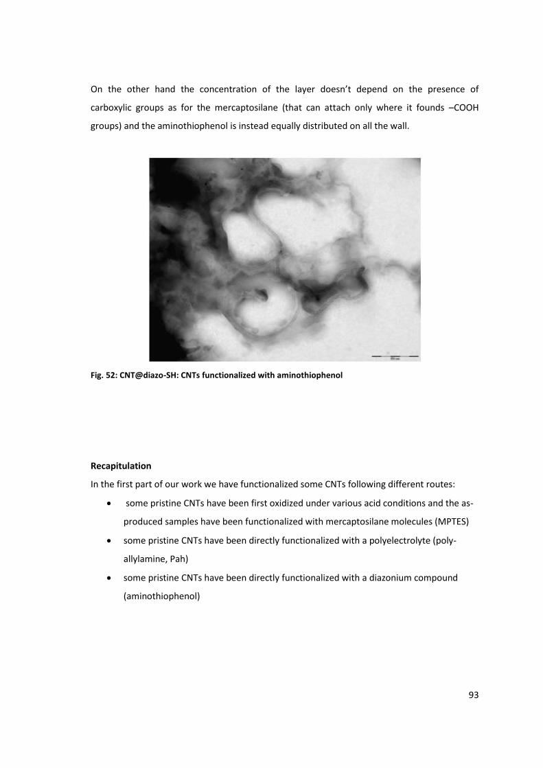
93
On the other hand the concentration of the layer doesn’t depend on the presence of
carboxylic groups as for the mercaptosilane (that can attach only where it founds –COOH
groups) and the aminothiophenol is instead equally distributed on all the wall.
Fig. 52: CNT@diazo-SH: CNTs functionalized with aminothiophenol
Recapitulation
In the first part of our work we have functionalized some CNTs following different routes:
some pristine CNTs have been first oxidized under various acid conditions and the as-
produced samples have been functionalized with mercaptosilane molecules (MPTES)
some pristine CNTs have been directly functionalized with a polyelectrolyte (poly-
allylamine, Pah)
some pristine CNTs have been directly functionalized with a diazonium compound
(aminothiophenol)

94
Then the samples available for further modifications are the following
sample Surface modification
CNT@mercaptosilane CNT oxidized and functionalized with a
mercaptosilane
CNT@Pah CNT functionalized with an electrolyte (Pah)
CNT@diazo-SH CNT functionalized with a diazonium
compound (aminothiophenol)

95
9. Synthesis of quantum dots
To synthesize CdS quantum dots we follow the polyol method. Indeed an alcohol with polar
and reductive characteristics is used as solvent. The most used polyols are some alpha-diols
like ethylene glycol (EG) and some glycol ethers such as diethylene glycol (DEG). The diols are
able to establish a lot of hydrogen bonds: this heightens their boiling temperature compared
to alcohols with the same number of carbons (ethanol: Tb = 78 °C; EG: Tb = 198 °C) as well as
their viscosity and water solubility.
For our purpose we use EG according to the method inspired to Fievet (1) and Feldmann’s work.
(2), (3) The advantage of this method resides in the possibility to lower the process
temperatures and to exploit the ability of the polyol to be the solvent for metallic ions and the
“environment” where NPs can grow up, the reducing agent, and sometimes a coupling agent.
We have tried to synthesize CdS NPs with different conditions taking advantage of the results
developed by a trainee within another project. (4) The method is always the same, the
differences consist in the kind of solvent, in the heating time, and presence of coupling agent.
The general procedure is the following: we start from reagents concentrations of 5*10-3 M in
120 ml of solvent (EG).
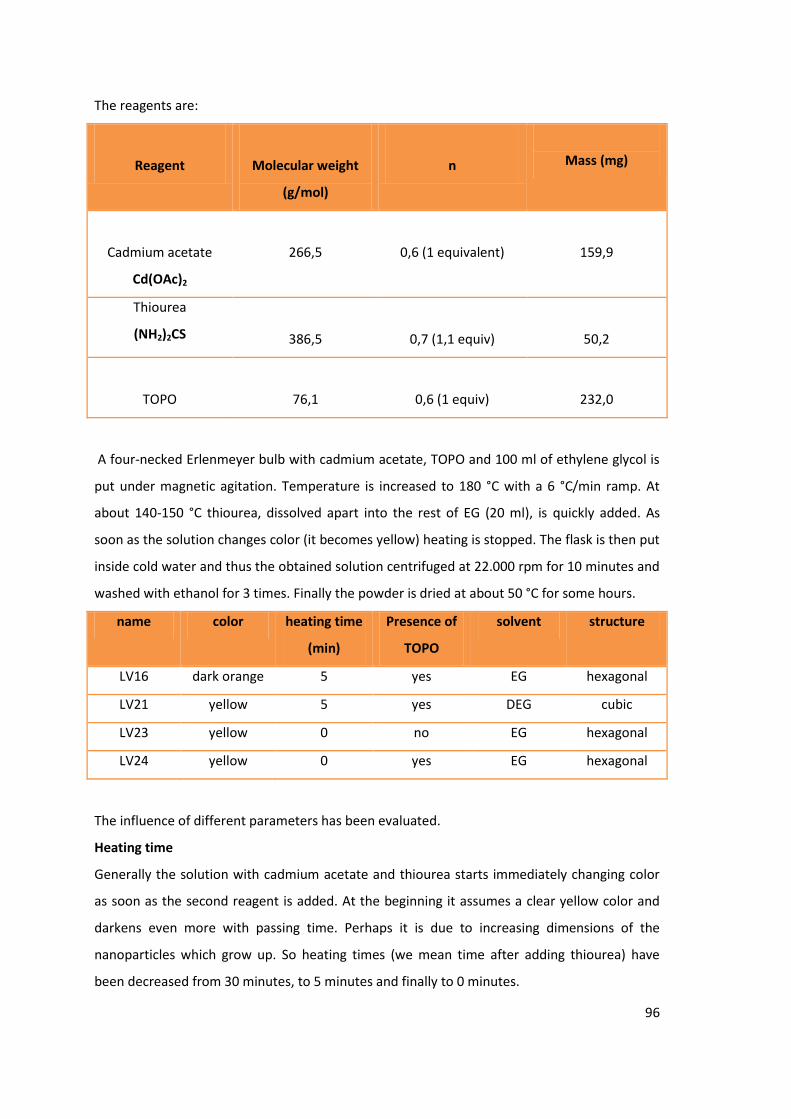
96
The reagents are:
Reagent Molecular weight
(g/mol)
n
Mass (mg)
Cadmium acetate
Cd(OAc)2
266,5 0,6 (1 equivalent) 159,9
Thiourea
(NH2)2CS 386,5 0,7 (1,1 equiv) 50,2
TOPO 76,1 0,6 (1 equiv) 232,0
A four-necked Erlenmeyer bulb with cadmium acetate, TOPO and 100 ml of ethylene glycol is
put under magnetic agitation. Temperature is increased to 180 °C with a 6 °C/min ramp. At
about 140-150 °C thiourea, dissolved apart into the rest of EG (20 ml), is quickly added. As
soon as the solution changes color (it becomes yellow) heating is stopped. The flask is then put
inside cold water and thus the obtained solution centrifuged at 22.000 rpm for 10 minutes and
washed with ethanol for 3 times. Finally the powder is dried at about 50 °C for some hours.
name color heating time
(min)
Presence of
TOPO
solvent structure
LV16 dark orange 5 yes EG hexagonal
LV21 yellow 5 yes DEG cubic
LV23 yellow 0 no EG hexagonal
LV24 yellow 0 yes EG hexagonal
The influence of different parameters has been evaluated.
Heating time
Generally the solution with cadmium acetate and thiourea starts immediately changing color
as soon as the second reagent is added. At the beginning it assumes a clear yellow color and
darkens even more with passing time. Perhaps it is due to increasing dimensions of the
nanoparticles which grow up. So heating times (we mean time after adding thiourea) have
been decreased from 30 minutes, to 5 minutes and finally to 0 minutes.

97
Resulting analysis show that the shorter the heating time and the more little and less
aggregated are the particles although polydispersity and a minor crystallization degree are
observed.
Fig. 53: LV16 (up) and LV24 (down): CdS NPs in ciclohexane
By looking at XRD spectra (fig.54) we can notice that peaks of LV-24 samples are not as well
defined as LV-16: this means that NPs obtained with 0 minutes of heating time are less
crystallized than the other ones.

98
Fig. 54: XRD spectrum of LV-16 and LV-24
EDX analysis let us to attribute the lower S and the higher O content of the samples with a
shorter heating time probably to a major quantity of defects.
Solvent
Synthesis performed inside EG yield yellow-orange NPs while in DEG they are of a rather light
yellow. We could hazard that this corresponds to different crystallographic phases and
particles dimensions: wurtzite (hexagonal crystal structure) for the former, with generally
bigger dimensions (always more than 4 nm), and zincblende (cubic structure) for the latter,
with diameters around 2-3 nm. In fact for example we see more defined peaks for LV-21
samples (fig.55) and larger peaks for LV-16 samples: this larger peaks, which could derive from
different NPs dimensions, could correspond to more than one peak that we are only not able
to separate.
20 40 60 80 100
500
1000
1500
2000
2500
3000
3500
4000
Co
up
s
2 (°)
LV-16 (5 min)
LV-24 (0 min)

99
Fig. 55: XRD spectrum of LV16 and LV21
Coupling agent
The presence of TOPO in the mixture has an ambiguous effect that cannot be well interpreted.
TOPO seems to play the part of “structuring agent”, promoting monodispersity and
crystallization.
However synthesis without TOPO produce particles with a dimension and aggregation
conditions similar to the others with TOPO.
Fig. 56: LV23 without TOPO

100
Unlike our expectation EDX and XPS analysis indicate that TOPO is absent on the NPs surface:
in fact the amount of phosphor detected is really weak. We can maybe hypothesize that TOPO
has left the nanoparticles during the centrifugation cycles.
Fig. 57: XPS spectrum of CdS quantum dots
Despite all at the end NPs result in more or less large aggregates (10-15 nm) that can be
annoying for further use of them (fig.58).
Fig. 58: LV16: presence of NPs aggregates
UV-VIS:
We have tried to get some information from UV-Vis spectra of CdS. (see chapter 11)

101
Recapitulation
We have synthesized CdS quantum dots in different conditions. Among all the samples we
choose the NPs obtained in ethylene glycol with TOPO as capping agent (LV-16). These NPs will
be subsequently mixed with the CNTs previously functionalized: CNT@mercaptosilane,
CNT@Pah, CNT@diazo-SH.

102
10. Nanohybrids formation
10.1 Solubility
We generally find out that pristine CNTs cannot be dispersed in any organic/aqueous solvent
even after sonication. For this reason they are usually functionalized by means of different
molecules or simply by oxidation techniques to solubilize them in solvents of interest.
According to the different compounds used to functionalize them they are able to be well-
dispersed in some organic solvents such as toluene after some sonication process; however
the suspensions are unstable because of competitive Van der Waals interaction between
nanotubes. After assembling NPs the CNT@NPs hybrids can be well solubilized in most of
common organic solvents such as toluene, THF, chloroform etc and the suspensions are stable.
The enhanced stability of the nanohybrids in common organic solvents can be due to some
combined effects: the NPs in fact can act as spatial blocking functions preventing the dispersed
nanotubes from aggregating again and at the same time play an important role in solubilizing
the hybrids as well as the functions grafted onto the CNTs’ surfaces do.
10.2 CNTs and QDs Solubility tests
After lots of tests the best solvents for solubilizing purposes result the following ones
CdS MWNT@diazo-SH MWNT@mercaptosilane MWNT@PAH
ethanol good good (with
sonication)
ok (after at least 1 h of
sonication)
no
toluene good no not so good unknown
DMF good good (light
yellow solution )
no unknown
THF good good no unknown
H20 quite
good
unknown unknown Ok (after at least 2 h
of sonication)

103
10.3 Mixing CNTs with QDs
As already said, our purpose is to graft quantum dots onto a modified CNT surface. To
accomplish this we have taken advantage of the well-known interaction between thiols and
metallic particles (5), (6), (7) and tried to extend this idea to the CdS quantum dots that we have
produced.
According to the HSAB theory (the Pearson acid base concept), most of the transition metal
semiconductor cations are soft acids; therefore it should be possible to well stabilize them
with soft bases. Then, polymer blocks functionalized with N, S, or P ligands are generally
applied. In our case Cd2+ present at the surface of QDs are soft acids and prefer to bond the
mercapto-groups, which are soft Lewis bases, so forming a rather covalent bond (only soft
acid-soft base bond is covalent). In the case of CdS/Zns core-shells maybe the bond is weaker
because of the “borderline” characteristic of the Zn2+ ions (more acid than Cd2+).
The covalent/ionic nature of the QD-ligand bond could be analysed through IR spectroscopy
(to assess the possible disappearance of the S-H bond at 2560-2580 cm-1).
So CNTs have been functionalized by means of some aryl/alkyl chains ending in thiol groups, i.e
aminothiophenol and mercaptosilanes.
We would further investigate the bond strength of a dithiocarbamate by comparison with a
single thiol. In fact the use of monothiol ligands makes QDs susceptible to oxidation. This
drawback has been overcome by using dithiocarbamate moieties as ligands due to their strong
chelate-type binding to metal atoms.
In literature some examples have been reported concerning the linkage between fullerenes
and quantum dots (8), (9) and TiO2 with CdSe/ZnS core-shells. (10)
Afterwards we have also tested the affinity between NH2 groups and the same CdS quantum
dots resting upon some literature advices (11), (12), (13).In the case of a primary amine maybe the
QD/ligand bond is weaker than with mercaptans.
10.3.1 Experiments
Because of missing information in interactions between thiol modified CNTs and QDs we didn’t
know the maximum amount of nanoparticles that can be grafted onto the CNTs surface, so we
just referred to some publications to try to put a right proportion of CdS nanoparticles. The
synthesis procedure was the following:
25 mg of CdS (LV-16) is solubilized inside a tube with 15 ml of ethanol and sonicated for 2
hours; the same thing is done with 10 mg of MWNT@Diazo-SH, still in 15 ml of ethanol.
Subsequently the two solutions are mixed together and sonicated for 30 minutes. The mixture
is than left all the night and seems to be stable the following day.

104
Fig. 59: two solutions: CNT@diazo-SH and CdS in ethanol
10 mg of CdS (LV-16) is solubilized inside 15 ml of ethanol and sonicated for 3 hours; 4 mg of
MWNT@mercaptosilane is put inside 15 ml of ethanol and sonicated for 3 hours (solubilization
of the mercaptosilane-functionalized CNTs is harder). Thus the two solutions are mixed,
sonicated for 30 minutes and let stand for the night. Unlike the previous synthesis the mixture
is not stable the following day: the CNT@CdS hybrids precipitate and deposit on the bottom of
the tube. Perhaps this is due to a lower amount of QDs present around the tubes, which in
theory prevent CNT bundles formation and then a more likely precipitation of the heavier
aggregates.
Fig. 60: two solutions: CdS and CNT@mercaptosilane (up left); two solutions mixed (up right); mixture
after night (down)

105
Due to dispersion problems of CdS nanoparticles and to try to avoid their aggregation, another
kind of synthesis has been performed:
CdS QDs have been prepared according to the already described polyol method with these
particular conditions: 1 equivalent of Cd(OAc)2 has been put into 120 ml of ethylene glycol,
without TOPO. The solution is stirred and heated till 150 °C, thus thiourea (1,1 equivalent) is
added and heating stopped as soon as it changes color, becoming yellow/orange.
Afterwards 5 mg of MWNT@diazo-SH has been sonicated for 2 hours inside 20 ml of ethanol.
They have been thus added to 20 ml of the previous solution (it should correspond to about
14/15 mg of CdS). The mixture of nanoparticles and solvents (EtOH and EG are miscible, even if
the mixture is initially made of two different phases) is put under ultrasounds for 1 hour. The
solution is not so stable: after few hours we have a phase separation. The product is called
ABQ1.
Fig. 61: mixture CNT@diazo-SH - ABQ1 before sonication
Fig. 62: CNT@diazo-SH@CdS, CNT@diazo-SH@ABQ1 and CNT@mercaptosilane@CdS just after
sonication

106
Fig. 63: CNT@diazo-SH@CdS, CNT@diazo-SH@ABQ1 and CNT@mercaptosilane@CdS after 1
sedimentation week
10.3.2 Results
TEM analysis
TEM analysis show that the interaction between CNT functions and CdS nanoparticles works
well for both the samples.
As MWNT@Diazo-SH is concerned, NPs distribution is quite uniform and involves all the CNT
wall (fig.64).
Fig. 64: CNT@diazo-SH@CdS
NPs grafted on MWNT@mercaptosilane are instead worse distributed along CNT wall: they are
localized in certain regions (fig.65) and especially in correspondence of CNT ends, where CNTs
result more modified, as we have stated before: in fact it’s at the ends of CNTs and at defect

107
sites that CNTs are greater oxidized and then there will be a bigger functionalization degree in
these zones.
Fig. 65: CNT@mercaptosilane@CdS
From TEM analysis (fig.66) we have seen that the chosen amounts of NPs are too huge: too
many QDs are present onto CNT surface (CdS aggregates simply deposited onto the surface).
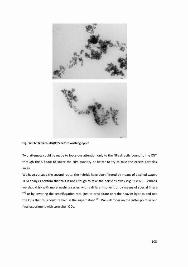
108
Fig. 66: CNT@diazo-SH@CdS before washing cycles
Two attempts could be made to focus our attention only to the NPs directly bound to the CNT
through the S-bond: to lower the NPs quantity or better to try to take the excess particles
away.
We have pursued the second route: the hybrids have been filtered by means of distilled water.
TEM analysis confirm that this is not enough to take the particles away (fig.67 e 68). Perhaps
we should try with more washing cycles, with a different solvent or by means of special filters
(14) or by lowering the centrifugation rate, just to precipitate only the heavier hybrids and not
the QDs that thus could remain in the supernatant (15). We will focus on the latter point in our
final experiment with core-shell QDs.

109
Fig. 67: CNT@mercaptosilane@CdS after washing cycles
Fig. 68-A: CNT@diazo-SH@CdS after washing cycles

110
Fig. 68-B: CNT@diazo-SH@CdS after washing cycles
An equally valid route could be offered by the introduction of CNTs directly inside the non-
centrifuged colloidal solution of QDs thus maybe encouraging a better dispersion of the NPs
along the CNT. These kinds of nanohybrids should then be subjected to some appropriate low-
rate centrifugation cycles.
This technique could also be used to finely control the amount of NPs we want to deposit on
the CNTs: we could put into the initial solution just the right quantity of precursors to get the
required amount of NPs and avoid a further centrifugation.
Fig. 69: CNT@diazo-SH@ABQ1: CNT inserted into the colloidal CdS solution (ABQ1)

111
Fig. 70: CNT@diazo-SH@ABQ1
XPS analysis
From XPS spectra we can get some general information as for example the presence of CdS
nanoparticles onto CNT surface.
Fig. 71-A: XPS spectrum of CNT@mercaptosilane@CdS

112
Fig. 71: XPS spectrum of CNT@diazo-SH@CdS
For MWNT@mercaptosilane we obtain an atomic percentage in Cd of 9,9 % and in S of 10,7 %:
we cannot distinguish between S belonging to CdS NPs and that one of mercaptosilane but we
can say for sure that a certain quantity of CdS is present (TEM analysis confirm this).
From the spectra we can clearly see the characteristic Cd doublet for 3d orbitals and that one
of S for 2p orbitals (fig.72).
Fig. 72: XPS high resolution spectra of Cadmium and Sulfur of CNT@mercaptosilane@CdS

113
The atomic percentages for MWNT@Diazo-SH are rather different from the previous ones.
Cd percentage reaches 22,1 % and it can be compared with S percentage (24,8 %), considering
that XPS measures are subjected to an error of 10 %.
In general data are less clear: for example the S peak doesn’t display the characteristic doublet
(fig.73), oxygen (16,12 %) is maybe too much (CNTs are not oxidized: it could be due to
oxidized Cd or more probably to oxygen of isoamyltnitrite physically adsorbed onto CNT
surface). We cannot assess nitrogen spectrum because of its superimposition with the Cd one.
Fig. 73: XPS high resolution spectrum of CNT@diazo-SH@CdS
10.3.3 Other essays
To assess the binding between MWNTs and CdS we have also tried to create other types of
mixtures, taking into account mainly the results obtained from other researchers in the field of
in-situ generation of NPs onto CNT surfaces (16). In fact in these publications NPs are supposed
to grow up mostly where -COOH groups or CNT irregularities are present. According to these
hints we have tried to make the following mixtures:
4,5 mg of pristine-MWNTs has been dispersed inside 15 ml of ethanol under ultrasounds for 3
hours; afterwards 11 ml (about 8 mg) of ABQ1 solution has been added and the mixture
sonicated for 1 hour.
4,5 mg of acid-oxidized MWNTs has undergone the same treatment.
The last attempt involves the mixing of CdS with (NH2)-modified-MWNTs. The nature of the
NH2-CdS bond has been inspired by solubility essays of quantum dots, (11) where these

114
nanoparticles were just modified by molecules with a double functionality to accomplish their
dispersibility in different solvents.
Then 1,1 mg of MWNT@COOH@Pah has been dispersed in 15 ml of distilled water and
sonicated for 2 hours. 2,3 mg of CdS has been sonicated into distilled water for the same time,
and the two solutions have been mixed and further sonicated for 30 minutes.
We have to notice that MWNT@Pah requires long sonication times to be dispersed into water
(into ethanol is impossible); besides CdS is much less soluble in water than in ethanol (there is
neither the presence of OH groups nor a capping agent which can stabilize the NPs).
TEM analysis
In the TEM images (fig.74 and 75) concerning the mixture between MWNT@Pah and CdS (LV-
16) quantum dots we can see that NPs seem anchored to the nanotubes but they are not well
distributed throughout the CNT: maybe this is due to an unsuccessful functionalization of
CNTs. Conversely NPs don’t form too big aggregates as in other synthesis, but are somewhere
present also in almost single units.
Fig. 74: CNT@Pah@CdS

115
Fig. 75: CNT@Pah@CdS
In the case of MWNT@CdS hybrids (fig.76 and 77), we can perceive a not so deep interaction
between the QDs and the CNTs: NPs seem to be collected in some chains or aggregates around
certain points and not to have a real contact with the nanotubes.
Fig. 76: CNT@CdS: pristine CNTs and CdS (ABQ1) quantum dots

116
Fig. 77: CNT@CdS
Also in the oxidized-CNTs/CdS mixtures NPs are chiefly localized in certain points (fig.78), that
are mainly CNTs ends, where maybe they are able to interact somehow with the carboxylic
functions.
As explained in literature, oxidized-CNTs cannot hold NPs that have not been synthesized in-
situ on nanotubes surface. The NPs aggregates can only stack up on the CNT and bundles
surfaces (fig.79).
Some photoluminescence studies would be interesting just to exclude any sort of electronic
communication.

117
Fig. 78: CNT@COOH@CdS: oxidized CNTs and CdS (ABQ1) quantum dots
Fig. 79: CNT@COOH@CdS

118
Summary
At this point we can sum up the nanohybrids we have obtained in our experimental work
sample Type of hybrid
CNT@mercaptosilane@CdS CNT@mercaptosilane + CdS (LV-16)
CNT@Pah@CdS CNT@Pah + CdS (LV-16)
CNT@diazo-SH@CdS CNT@diazo-SH + CdS (LV-16)
CNT@diazo-SH@ABQ1 CNT@diazo-SH + CdS (ABQ1)
CNT@CdS Pristine CNT + CdS (ABQ1)
CNT@COOH@CdS Oxidized CNT + CdS (ABQ1)
We have seen that CNTs don’t deposit onto the walls of pristine and oxidized CNTs. The
synthesis with the polyelectrolyte (Pah) has to be improved but it is promising for a good
nanotube coverage. At the same way the introduction of CNTs inside the non-centrifuged
colloidal solution of the QDs could lead to a good CNT/QDs interaction maybe preventing NPs
aggregation issues.
The more striking result involves the difference in CNT coverage when nanotubes are
functionalized with a mercaptosilane or through diazonium chemistry. For the first case, NPs
appear more localized in the zones of the nanotube where the functionalization degree is
probably higher (which corresponds to the initial presence of more –COOH groups in the
oxidized nanotubes), that is at the nanotube ends and near the defects of the pristine CNTs; in
CNT@diazo-SH@CdS nanohybrids the NPs seem to be present along all the CNT wall. This fact
could be differently exploited for various targets.
However we have just highlighted the presence of NPs on CNT walls. We haven’t described
their electronic interaction yet.

119
11. Uv-Vis and Photoluminescence analysis
We have probably reached the most interesting part of our work which could let us evaluate
the effectiveness of the electronic interaction between the QDs and CNTs. In fact we have
hypothesized the presence of CdS nanoparticles onto the surface of CNTs by means of XPS
measurements, we have physically observed their presence through TEM analysis but we have
never verified the real communication between the two main actors of our device. The final
goal should be that of harvesting the sunlight, that is capturing it and allowing its
“exploitation”, thus converting it into ready-for-use electric energy. We have already
acknowledged the light-catching properties of QDs and the electrical conducting ability of
CNTs. So we have to focus our attention on the mechanism that lets the device pursue the
light-electricity conversion, namely the CNTs/QDs communication skills. UV-Visible absorption
and Photoluminescence analysis can provide some more information about it.
11.1 UV-VIS absorption analysis
After having assured that TOPO (maybe present onto QDs surfaces) doesn’t absorb light
between 300 and 800 nm, we have analyzed two CdS samples:
CdS2: LV16 with ethanol as reference: 0,5 mg / 5 ml = 10-1 M
CdS6: ABQ1 with EG : 0,125 mg / 5 ml = 2,5*10-2 M
Afterward UV-Vis analysis of the following samples have been performed:
NTD1 : MWNT@diazo-SH in ethanol: 2 mg / 5 ml = 4*10-1 M
NTM1 : MWNT@MPTES in ethanol: 2 mg / 5 ml = 4*10-1 M
NTCdS3: we use the solution ABQ1* (made of two solvents: EG and ethanol, so the
reference takes into account the presence of both of them): about 0,32 mg of
MWNT@diazo-SH / 5 ml of EG = 6,4*10-2 M
NTDCdS3: 0,4 mg of ABD162 / 5 ml of ethanol = 8*10-2 M
NTMCdS2: 0,24 mg of ABME16-(washed) / 5 ml of ethanol = 4,8*10-2 M
All the solutions have been previously sonicated and not all of them reach a high solubility
(some particles remain on the bottom of the cuvettes), so the quantities above mentioned are
purely indicative. Because of the different concentrations among the samples, the spectra
cannot be quantitatively compared, a more accurate analysis is worth being performed.
However, we can draw some useful conclusions from the spectra.

120
Fig. 80: “CdS2” (LV16) absorption spectrum
As far as the CdS (LV16) spectra are concerned (fig.80), we can highlight the presence of a
shoulder at 467 nm that identifies the peak correspondent to the gap of the nanoparticles
(1S(e)-1S transition). This peak is rather broadened and not too marked, moreover the
absorption onset is not well defined, thus maybe involving the presence of a polydispersion of
the NPs dimensions and some surface defects which allow absorption at wavelengths longer
than the gap width.
Fig. 81: “CdS6” (ABQ1) absorption spectrum
300 400 500 600 700 800
0,2
0,3
0,4
0,5
0,6
0,7
0,8
0,9
1,0
Ab
so
rba
nce
(nm)
CdS (LV-16)
300 400 500 600 700 800
0,0
0,2
0,4
0,6
0,8
1,0
Ab
so
rba
nce
(nm)
CdS (ABQ1)

121
For the ABQ1 CdS samples (fig.81) the shoulder is more or less at the same position (about 460
nm), but the absorption onset is more defined. We have to say that this spectra belongs to the
QDs still dispersed in the solutions, so not yet centrifuged and redispersed. So maybe NPs are
subjected to some “alterations” after the centrifugation cycles: perhaps this is due to the loss
of the capping agent.
Glancing at the spectra of the nanohybrids we can remark a substantial similarity to the
spectra of the CdS quantum dots, and this is what we expected. By attentively observing it, it is
possible to see the presence for the CNT@diazo-SH@CdS nanohybrids (fig.82) of the same
exciton peak as CdS quantum dots alone, and a relative equality between the two spectra. The
fact that the QD absorption edge can be distinguished can only be explained by a dense
coating of relative monodisperse QDs onto the CNTs (15).
300 400 500 600 700 800
0,2
0,3
0,4
0,5
0,6
0,7
0,8
0,9
1,0
Asso
rba
nza
(nm)
CNT@diazo-SH@CdS
Fig. 82: Absorption spectrum of CNT@diazo-SH@CdS(LV16) nanohybrids
In the CNT@mercaptosilane@CdS (fig.83) we lose the presence of the band-edge peak but the
rest of the spectrum is quite similar. Maybe this is due to the more feeble quantity of CdS
quantum dots on the nanotubes.

122
300 400 500 600 700 800
0,3
0,4
0,5
0,6
0,7
0,8
0,9
1,0
Asso
rba
nza
(nm)
CNT@mercapto-SH@CdS
Fig. 83: Absorption spectrum of CNT@mercaptosilane@CdS(LV16) nanohybrids
Afterward if we compare the spectra of CdS quantum dots “ABQ1” with that of the
CNT@diazo-SH mixed directly to the CdS solution (fig.84) we can still see the exciton peak at
the same wavelength as well as a slightly different absorption profile at shorter wavelengths as
well: another shoulder can be seen at about 360 nm, maybe corresponding to higher energies
transitions (1P(e)-1P).
300 400 500 600 700 800
0,0
0,2
0,4
0,6
0,8
1,0
1,2
Asso
rba
nza
(nm)
CdS
CNT@diazo-CdS
Fig. 84: Absorption spectrum of CdS (ABQ1) NPs and CNT@diazo-SH@CdS nanohybrids

123
In the end from the PL spectra of CdS quantum dots that we have synthesized we can notice
the lack of luminescence. Then we have chosen to utilize some commercial quantum dots (see
below) to evaluate the effectiveness of the CNT/QDs coupling. Their absorption spectrum is
shown (fig.85): a shoulder is absent but of a more definite and less broadened peak is present
at about 593 nm.
400 500 600 700
0,0
0,1
0,2
0,3
Asso
rba
nza
(nm)
QDs Maple-red orange
Fig. 85: Absorption spectrum of CdS/ZnS “Maple-red orange” commercial QDs
11.2 Photoluminescence
More than UV-Vis spectra, PL spectra can shed some light on the communication
characteristics between QDs and CNTs.
Unfortunately some problems arose with the CdS NPs that we have synthesized and used in
most of our nanohybrids. In fact from PL analysis we have seen that they are not luminescent;
maybe this is due to aggregation issues, or to other non-radiative mechanisms that prevent a
luminescent response.
So we have had to utilize something else to test our device: our availabilities consisted of some
commercial core-shell quantum dots with a CdS core and a ZnS shell.
11.2.1 Experiments
For our synthesis we have used some commercial CdS/ZnS quantum dots: the Eudent Maple
Red Orange. The only information we are provided is their structure: they are core-shell
quantum dots with a nucleus of CdS and some outer layers of ZnS (we don’t know the

124
thickness). They are dispersed in toluene in a concentration that should correspond to 19,5
mM.
Their characteristics are thus different from our homemade CdS quantum dots; however we
have tried to insert them on our nanohybrids to study their optical properties.
First of all we had to test their solubility properties. We didn’t know the original capping agent
present on the nanoparticles, but we have realized that this quantum dots were not soluble in
ethanol, yet since all our synthesis are performed in this solvent we needed to disperse them
in it. Consequently we have tried to find the proper capping agent to reach this purpose. We
have first tried to see if the particles could precipitate thanks to conjugation with the 6-
mercapto-1-hexanol. From these essays one can infer that our QDs weren’t capped with some
thiol functionalities. Thereby we have switched to some amines: from the precipitation of the
QDs by means of the 5-amino-1-penthanol in chloroform we have then hypothesized that the
capping agent were an amine. We have then centrifuged our core-shells, washed them in
chloroform to take all the previous capping agent out, and finally dispersed into ethanol thanks
to the capping action of short chains of amino-penthanol: they resulted stable in solution.
Eventually our NPs were ready to go on with the synthesis.
From TEM analysis (fig.86) we can see that our core-shells are composed of well dispersed NPs
that don’t present aggregation problems.
Fig. 86: CdS/ZnS core-shells in ethanol
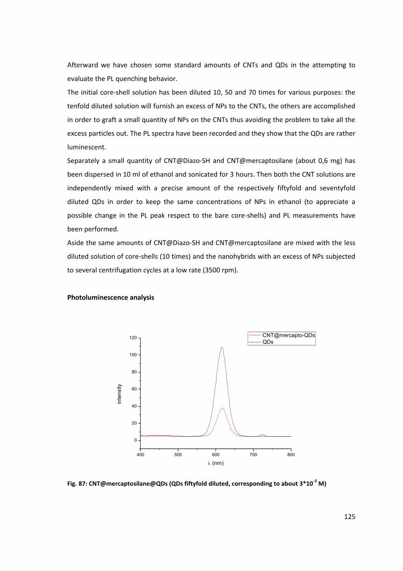
125
Afterward we have chosen some standard amounts of CNTs and QDs in the attempting to
evaluate the PL quenching behavior.
The initial core-shell solution has been diluted 10, 50 and 70 times for various purposes: the
tenfold diluted solution will furnish an excess of NPs to the CNTs, the others are accomplished
in order to graft a small quantity of NPs on the CNTs thus avoiding the problem to take all the
excess particles out. The PL spectra have been recorded and they show that the QDs are rather
luminescent.
Separately a small quantity of CNT@Diazo-SH and CNT@mercaptosilane (about 0,6 mg) has
been dispersed in 10 ml of ethanol and sonicated for 3 hours. Then both the CNT solutions are
independently mixed with a precise amount of the respectively fiftyfold and seventyfold
diluted QDs in order to keep the same concentrations of NPs in ethanol (to appreciate a
possible change in the PL peak respect to the bare core-shells) and PL measurements have
been performed.
Aside the same amounts of CNT@Diazo-SH and CNT@mercaptosilane are mixed with the less
diluted solution of core-shells (10 times) and the nanohybrids with an excess of NPs subjected
to several centrifugation cycles at a low rate (3500 rpm).
Photoluminescence analysis
400 500 600 700 800
0
20
40
60
80
100
120
inte
nsity
(nm)
CNT@mercapto-QDs
QDs
Fig. 87: CNT@mercaptosilane@QDs (QDs fiftyfold diluted, corresponding to about 3*10-3
M)

126
400 500 600 700 800
0
20
40
60
80
100
120
inte
nsity
(nm)
QDs
CNT@diazo-QDs
CNT@diazo
Fig. 88: CNT@diazo-SH@QDs (QDs fiftyfold diluted, corresponding to about 3*10-3
M)
400 500 600 700 800
-5
0
5
10
15
20
25
30
35
40
45
50
55
60
inte
nsity
(nm)
CNT@diazo-QDs
QDs
CNT@diazo
Fig. 89: CNT@diazo-SH@QDs (QDs seventyfold diluted, corresponding to about 2*10-3
M)
These spectra have been recorded just after the synthesis, however no significant changes
occur after longer periods of time. The samples have been excited to 360 nm, with wavelength
corresponding to the maximum of luminescence for the QDs.
We can basically notice that the quantum dots peak is well defined and corresponds to the
band-edge emission: it is about 20 nm red-shifted compared to the corresponding absorption
exciton peak. Besides the functionalized CNTs do not emit in the visible wavelength range.
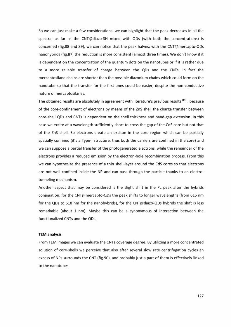
127
So we can just make a few considerations: we can highlight that the peak decreases in all the
spectra: as far as the CNT@diazo-SH mixed with QDs (with both the concentrations) is
concerned (fig.88 and 89), we can notice that the peak halves; with the CNT@mercapto-QDs
nanohybrids (fig.87) the reduction is more consistent (almost three times). We don’t know if it
is dependent on the concentration of the quantum dots on the nanotubes or if it is rather due
to a more reliable transfer of charge between the QDs and the CNTs: in fact the
mercaptosilane chains are shorter than the possible diazonium chains which could form on the
nanotube so that the transfer for the first ones could be easier, despite the non-conductive
nature of mercaptosilanes.
The obtained results are absolutely in agreement with literature’s previous results (14) : because
of the core-confinement of electrons by means of the ZnS shell the charge transfer between
core-shell QDs and CNTs is dependent on the shell thickness and band-gap extension. In this
case we excite at a wavelength sufficiently short to cross the gap of the CdS core but not that
of the ZnS shell. So electrons create an exciton in the core region which can be partially
spatially confined (it’s a Type-I structure, thus both the carriers are confined in the core) and
we can suppose a partial transfer of the photogenerated electrons, while the remainder of the
electrons provides a reduced emission by the electron-hole recombination process. From this
we can hypothesize the presence of a thin shell-layer around the CdS cores so that electrons
are not well confined inside the NP and can pass through the particle thanks to an electro-
tunneling mechanism.
Another aspect that may be considered is the slight shift in the PL peak after the hybrids
conjugation: for the CNT@mercapto-QDs the peak shifts to longer wavelengths (from 615 nm
for the QDs to 618 nm for the nanohybrids), for the CNT@diazo-QDs hybrids the shift is less
remarkable (about 1 nm). Maybe this can be a synonymous of interaction between the
functionalized CNTs and the QDs.
TEM analysis
From TEM images we can evaluate the CNTs coverage degree. By utilizing a more concentrated
solution of core-shells we perceive that also after several slow rate centrifugation cycles an
excess of NPs surrounds the CNT (fig.90), and probably just a part of them is effectively linked
to the nanotubes.

128
Fig. 90: CdS/ZnS core-shells onto CNT@diazo-SH after several centrifugation cycles
Instead when the NP concentration is consistently decreased NPs result well disposed on the
CNT walls. The situation is better defined in CNT functionalized with diazonium compounds
(fig.91), where it seems that all the NPs in solution are attached to the nanotubes (the
samples didn’t undergo centrifugation); it is a bit more confused in CNTs functionalized with
the mercaptosilane (fig.92) where somewhere we notice some NPs aggregations, perhaps in
correspondence of the CNT ends, and we don’t know if it stands for a too high NPs
concentration or to a weaker CNT-NPs interaction but because of the more reliable
photoluminescence response we are inclined to the first hypothesis. Even XPS should confirm
our assumptions, in fact the percentage of sulfur on the CNT@mercaptosilane wall is lower
than for the CNT@diazo-SH, thereby the NPs concentration (the same as for diazonium
compounds) is maybe still too high.
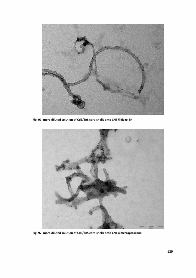
129
Fig. 91: more diluted solution of CdS/ZnS core-shells onto CNT@diazo-SH
Fig. 92: more diluted solution of CdS/ZnS core-shells onto CNT@mercaptosilane

130
Fig. 93: more diluted solution of CdS/ZnS core-shells onto CNT@mercaptosilane
Centrifugation cycles
As for the previous synthesis also this time we have used some excess of QDs when mixed with
CNTs. However the mixtures have undergone some low speed centrifugation cycles in order to
let only to heavier CNTs deposit on the tubes bottom with the aim of removing the excess
particles present in the supernatant.
TEM images of the gathered hybrids show still a big amount of NPs all around the CNTs which
probably aren’t all linked to the surface but just leant to each other (fig. 94 and 95).

131
Fig. 94: CdS/ZnS core-shells onto CNT@diazo-SH after centrifugation
Fig. 95: CdS/ZnS core-shells onto CNT@diazo-SH after centrifugation
On the other hand, from TEM analysis of the supernatant we can notice the presence of a
great deal of NPs and only few isolated CNTs: this could mean that the adopted technique
holds good. Perhaps the centrifugation rate can still be lowered.

132
12. Conclusion and future work
Our experimental work aimed at synthesizing two kinds of CNT/QDs nanohybrids.
On the one hand pristine CNTs have been oxidized and further functionalized with a
mercaptosilane, on the other hand, pristine CNTs have undergone a non-covalent
functionalization by means of diazonium compounds.
Functionalization with mercaptosilane has been accomplished on oxidized CNTs, thus it
involved principally the end parts of CNTs and the ones with defects. Diazonium salts allow to
better functionalize all the CNT walls. Despite this, it was difficult to create just a monolayer of
the aromatic compound and this could be penalizing for use in photovoltaic applications where
a direct contact between NP and CNT is more desirable.
However XPS and TEM measurements have confirmed the clear and fundamental presence of
thiol functions in anchoring NPs to CNT surface in both the obtained samples. In fact other
attempts have revealed a missing interaction between pristine and oxidized CNTs and the
nanoparticles.
The amount of NPs anchored to CNTs has to be optimized. We can follow two routes: either
functionalized CNTs can be directly dispersed into a colloidal solution of nanoparticles or an
imprecise quantity of quantum dots can be mixed to nanotubes and the hybrid centrifuged to
low rates in order to take the excess NPs out.
Photoluminescence spectroscopy has suggested CNT/QDs communication skills. In all samples
analyzed a decrease in the PL peak has been observed: it roughly halves in CNT@diazo-
SH@QDs nanohybrids and reaches almost one third of the original height in
CNT@mercaptosilane@QDs. This highlights an interaction between the semiconductors and
the nanotubes but it is impossible to determine whether the incomplete PL quenching is
effectively due to the core confinement of electrons in the type-I structures which hampers
the transfer of charge or to the type of CNT functionalization. Substitution with type-II core-
shells in the nanohybrids is stimulated.
As far as the CNT functionalization with a polyelectrolyte is concerned some promising results
have been obtained: that pushes to optimize the synthesis procedure and test the amine
function-QDs interaction with photoluminescence measurements.
Moreover it will be interesting to compare the electric communication in our nanohybrids with
other hybrids functionalized with some dithiol functions to see if their anchoring and transfer
of charge ability is higher.

133
The particular conformation of CNT@mercaptosilane hybrids suggests to exploit the
functionalization with organosilanes in CNT forests directly grown up on the electrodes. In fact
the simple deposition on single functionalized-CNTs on the surface of the electrodes or in
other matrices prevents obtaining high efficiencies in the respective devices because of charge
dispersion.
Substitution of CNTs with TiO2 nanotubes could be another practicable route that could be
exploited in DSSCs. Generally Grätzel cells make use of TiO2 nanoparticles and because of the
porous structure the transport of charge is not optimal; an electron acceptor tubular structure
could facilitate the electrons mobility.

134
13. Bibliography
1. F. Fievet, J.P. Lagier et al, Solid State Ionics, (1989)
2. C.Feldmann, Advance Functional Materials, 13, (2003), No.2, 101
3. C.Feldmann, C.Metzmacher, Journal of Material Chemistry, (2001), 11, 2603
4. Lydie Vivet, Incorporation d’ions Gd3+ dans des nanoparticules de semi-conducteurs pour
l’élaboration de sondes bimodales pour l’imagerie médicale, Rapport de stage, (2010)
5. Jin Shi, Zhe Wang, Hu-lin Li, Journal of Nanoparticlen Research, (2006), 8, 743
6. Jui-Ming Yeh, Kuan-Yeh Huang et al, Journal of Nanotechnology, (2009)
7. Jin Shi, Yu-Qi Hu, Yi-Xin Hua, Electroanalysis 20, (2008), 13, 1483
8. Dongfang Liu, Wei Wu, Shihe Yang, J. of Physics and Chemistry of Solids 70, (2009), 694
9. Dongfang Liu, Wei Wu et al, Journal of Physical Chemistry C, (2007), 111, 17713
10. Jun Wang, Jun Xu et al, Journal of Materials Chemistry, (2008), 18, 3270
11. M.Olek, T.Busgen et al, J. Phys. Chem. B, (2006), 110, 12901
12. Yunlong Zeng, Chunran Tang et al, Spectrochimica Acta Part 70, (2008), 966
13. X. Li, Yi Jia, A. Cao, AcsNano, vol.4, (2010), 1, 506
14. S.Jeong, H.C.Shim et al, AcsNano, vol.4, (2010), 324
15. H.Y.Si, C.H.Liu et al, Nanoscale Res Lett, (2009), 4, 1146
16. F.Li, S.H.Cho et al, Applied Physics Letters, (2009), 94, 111906
17. Miao Feng, R.Sun et al, Carbon 48, (2010), 1177
18. Z.Zhu, R.Yang et al, Anal Bioanal Chem, (2010), 396, 73
19. G.Mountrichas, A.S.D. Sandanayaka et al, J.Mater.Chem., (2009), 19, 8990
20. B.Farrow, P.V.Kamat, J.Am.Chem.Soc., (2009), 131, 11124
21. I.Robel, B.A.Bunker, P.V.Kamat., Adv. Mater. (2005) 17 2458
22. T.C.W.Mak, K.S.Jasim, C.Chieh, Can. J. Chem., 62 (1984), 808
23. L.A.Ramos, E.T.G.Cavalheiro, G.O.Chierice, Journal of Thermal Analysis and Calorimetry,
vol. 79, (2005), 349
24. Synthesis of new dithiocarbamates. Hu, Zhenshan et al. 1986.

135
25. S.Goubert-Renaudin, R.Schneider, A.Walcarius, Tetrahedron letters 48, (2007), 2113
26. V.K.Tiwari, A.Singh et al, Monatshefte fur Chemie, 138, (2007), 653
27. L.Sheeney-Haj-Ichia, et al, Angew. Chem. Int. Ed. (2005) 44, 78
28. C.A.Dyke, M.P.Stewart et al, Diazonium-based functionalization of Carbon Nanotubes. XPS
and GC-MS analysis and mechanistic implications, (2003)
29. P.R.Marcoux, P.Hapiot,P.Batail and J.Pinson, New. J. Chem, (2004), 28, 302
30. R.L.McCreery, B.L.Hurley and, Journal of the electrochemical society, (2004), 151(5), B252
31 L.Sheeney-Haj-Ichia, et al, Angew. Chem. Int. Ed. (2005) 44, 78
32 . D.Yu.Parashchuk, A.I.Kokorin, Russian Journal of General Chemistry (2009) 11 2543
33. P.Brown,K.Takechi, V.Kamat, J. Phys. Chem. C (2008) 112 4776
34. Chuan-Yu Yen, Yu-Feng Lin et al, Nanotechnology (2008) 19 375305
35. T.Y. Lee, P.S.Alegaonkar, Ji-Beom Yoo, Thin solid films (2006) 5131
36. I. Mora-Sero’,S.Giménez et al, Accounts of chemical research (2009)
37. D.M. Shewchuk, M.T. McDermott, Langmuir Article, (2009), 25(8), 4556
38. J.L Delgado, M.A. Herranz, N. Martin, Journal of Material Chemistry (2008) 18 1417.
39. D. Tasis, N. Tagmatarchis, et al, Chem. Rev. (2006) 106 1105.
40. Y. Xing, J. Phys. Chem. B (2004) 108 19255.
41. P.R. Marcoux, P. Hapiot et al, J. New J. Chem. 28 (2005) 302
42. W. Wu, N.V. Tsarevsky, et al, Small (2007) 3 1803.
43. M. Grzelczak, A. Correa-Duarte, L.M. Liz-Marzan, Small (2006) 2 1174
44. A.M. Gilmore, Nanophotonics, Proc. of Spie, Vol. 6195, (2006), 61950M-1
45. A. Hartschuh, H.N. Pedrosa et al, ChemPhysChem, (2005), 6, 1
46. S. Baskoutas, A.F. Terzis, J. Appl. Phys., (2006), 99, 013708
47. A.M.Smith, S. Nie, Accounts of chemical research, (2009)
48. O. Ovits, R. Tel-Vered et al, J. Mater. Chem., (2009), 19, 7650

136

137
Ringraziamenti
In ordine assolutamente sparso tengo a ringraziare
La prof.ssa Giovanna Brusatin, per avermi spedito in Francia con il rapido dell’11 marzo 2010
La prof.ssa Fayna Mammeri, per avermi accolto all’arrivo del rapido dell’11 marzo, nel
laboratorio multietnico che ha cominciato a farmi amare Parigi, dimenticando quella sana e
riconosciuta antipatia che accomuna i nostri due popoli
Marion Giraud, per aver sostenuto il mio lavoro, e per avere una casa a Parigi, che potrebbe
fare presto la mia conoscenza.
Il quarto, quinto, sesto, ottavo piano dell’Itodys, mi è mancato solo il settimo, ma mai dire mai.
Luciano, per essere italiano, ed anche per essersi sorbito le mie richieste assieme a Guillaume
M.Chehimi, Samia, Chantal, il China-team & dintorni e tutti quelli che in un modo o nell’altro
sono stati presenti durante il mio lavoro
Torniamo in Italia.. grazie ai miei compagni di corso, per essere tutti diversi l’uno dall’altro, e
scampare un po’ al prototipo di ingegnere “sfigato”
Grazie alla mia famiglia, perché è la mia famiglia
Grazie ad amici di oggi e di allora, perché mi sono sempre intorno
Grazie a chi non è incluso in questa lista, perché sarà incluso in un’altra, più approfondita, mai
stampata!