functionalizationofsi(111)surfacesandtheformationof...
TRANSCRIPT

Functionalization of Si(111) surfaces and the formation ofmixed monolayers for the covalent attachment of molecular
catalysts in photoelectrochemical devices
Thesis by
Judith Rebecca Cabelli Lattimer
In Partial Fulfillment of the Requirements
for the Degree of
Doctor of Philosophy
California Institute of Technology
Pasadena, California
2014
(Defended April 21, 2014)

ii
© 2014
Judith Rebecca Cabelli Lattimer
All Rights Reserved

iii
This work is dedicated to the memory of my beloved Saba, Victor Cabelli, who shared with
me his love for science, his love for family, and his birthday.

iv
Acknowledgments
My research advisor, Harry Gray, is one of the most outgoing and enthusiastic people I have
ever met. His overwhelming love of science and affection for his students made his group a
truly wonderful place to be a graduate student, and I can’t thank him enough for welcoming
me into his group. Thanks also to Bruce Brunschwig, who really directed my research project
and was always available to discuss my latest results, or lack thereof. Working together in
the MMRC I learned so much about instrumentation and the importance of plumbing. While
I was formally a member of Gray Nation, my research project grew out of work done in Nate
Lewis’s group, and I would like to thank Nate for allowing me to be an unofficial member of
the Lewis group. I learned so much from Nate and his students, and I am so grateful for that
opportunity. Thanks also to Mitchio Okamura and Theo Agapie for all the feedback and
advice they provided at my committee meetings and exams. The entire Caltech chemistry
faculty makes this school and division a truly welcoming place to be a graduate student, and
I could not have asked for a better committee.
I could not have joined a better research group than the Gray group. The depth and
breadth of knowledge exhibited by everyone in the group meant that there was always
someone who could provide insight on whatever problem had come up. Surface science is
hard, and I’m grateful to the many Gray and Lewis groupers with whom I tackled this
problem over the years. Leslie O’Leary showed me the ropes when it came to silicon surface
chemistry, got me started on my project, showed me how to do electrochemistry and how to
use all the surface science instruments, and has been an endless source of help for my entire
graduate career. Thank you. My collaboration with James Blakemore over the past few
years on the bipy work has been invaluable and I am so glad that we had this opportunity to
work together. My thanks also to Mike Rose, with whom I did much of the early work on the
cross-coupling project. Special thanks to Wesley Sattler and Maddie Radlauer (of the Agapie
group) for providing me with chemicals I did not have the expertise to synthesize myself.

v
Thanks to David Gleason-Rohrer for training me first to use the XPS, and then to maintain
it. Joseph Beardslee, my fellow XPS GLA, made instrument maintenance a lot more fun
and taught me a lot about high vacuum systems, for which I am grateful. Thanks to Adam
Nielander, Noah Plymale, and Amanda Shing for taking up the XPS GLA torch. Thanks to
Erik Johansson for training me on the FTIR. Thanks to Ron Grimm and his instrumentation
expertise, which kept the lab running, and training me on the SRV set-up. Thanks to Rob
Coridan for being a great and incredibly helpful officemate. Thanks to Gretchen and Oliver,
who made sure that there was no better party than a Gray group party.
Graduate school would have been unbearable if not for the incredible group of friends I
managed to find here at Caltech. Most of all, I want to thank Maggie Thompson. You’re
my best friend and you’re crazy. I love you. Ethan Van Arnam, Alex Goldberg, James
McKone, Kirsten Peterson, Taylor Lenton, Tim Mui, Sigrid and Dan Barklund, Kaycie
and Casey Deyle, Maraia Ener, and Rob Usiskin - Our Saturday morning farmer’s market
expeditions which morphed into brunches and “family” dinners were so much fun and kept life
in perspective. I got to call so many of you “roommate” over the years at so many different
addresses, and each of those experiences was special in its own way. The past year or so has
really been defined by my time with John Bruer, Scott Steger, Trevor Fowler, and Mark
Giacomantonio. I am so grateful to you guys for having a pool, being so generous with your
television, and letting me become an unofficial roommate. A special thanks to John for his
computer skills – I couldn’t have done it without you.
Finally, I want to thank my family. My parents are incredible role models, having gone
through grad school themselves, and were always supportive of my research, constantly asking
why I was talking to them and not in the lab. They are actually among my greatest scientific
resources, and I love and appreciate them more than I can say. My siblings, Jennifer, Julia,
and Jonathan, are the most important people in the world and I love that they all managed
to come out to visit me during my time at Caltech, despite the distance. Thanks also to
my entire extended family, from Savta and Grandma down through the generations to the
multitude of baby cousins I managed to acquire while in grad school. My trips back East to
see them, and my future brother-in-law Stephen and new niece Vivienne, made everything
seem better. I am so lucky to have such a wonderful and supportive family.

vi
Abstract
The functionalization of silicon surfaces with molecular catalysts for proton reduction is
an important part of the development of a solar-powered, water-splitting device for solar
fuel formation. The covalent attachment of these catalysts to silicon without damaging the
underlying electronic properties of silicon that make it a good photocathode has proven
difficult. We report the formation of mixed monolayer-functionalized surfaces that incor-
porate both methyl and vinylferrocenyl or vinylbipyridyl (vbpy) moieties. The silicon was
functionalized using reaction conditions analogous to those of hydrosilylation, but instead of
a H-terminated Si surface, a chlorine-terminated Si precursor surface was used to produce
the linked vinyl-modified functional group. The functionalized surfaces were characterized
by time-resolved photoconductivity decay, X-ray photoelectron spectroscopy (XPS), electro-
chemical, and photoelectrochemical measurements. The functionalized Si surfaces were well
passivated, exhibited high surface coverage and few remaining reactive Si atop sites, had a
very low surface recombination velocity, and displayed little initial surface oxidation. The
surfaces were stable toward atmospheric and electrochemical oxidation. The surface coverage
of ferrocene or bipyridine was controllably varied from 0 up to 30% of a monolayer without
loss of the underlying electronic properties of the silicon. Interfacial charge transfer to the
attached ferrocene group was relatively rapid, and a photovoltage of 0.4 V was generated upon
illumination of functionalized n-type silicon surfaces in CH3CN. The immobilized bipyridine
ligands bound transition metal ions, and thus enabled the assembly of metal complexes on
the silicon surface. XPS studies demonstrated that [Cp∗Rh(vbpy)Cl]Cl, [Cp∗Ir(vbpy)Cl]Cl,
and Ru(acac)2vbpy were assembled on the surface. For the surface prepared with iridium,
x-ray absorption spectroscopy at the Ir LIII edge showed an edge energy and post-edge
features virtually identical to a powder sample of [Cp∗Ir(bipy)Cl]Cl (bipy is 2,2´-bipyridyl).
Electrochemical studies on these surfaces confirmed that the assembled complexes were
electrochemically active.
vii
Contents
Acknowledgments iv
Abstract vi
1 Background and Motivation 1
1.1 Solar Energy . . . . . . . . . . . . . . . . . . . . . . . . . . . . . . . . . . . . 1
1.2 Semiconductor Photoelectrochemistry . . . . . . . . . . . . . . . . . . . . . . 4
1.3 Silicon Surface Modification . . . . . . . . . . . . . . . . . . . . . . . . . . . . 7
2 Cross Metathesis Reactions on Silicon Surfaces using the Grubbs’ Catalyst,
2nd Generation 11
2.1 Introduction . . . . . . . . . . . . . . . . . . . . . . . . . . . . . . . . . . . . . 11
2.2 Mixed Methyl/Allyl Surfaces and Reactions . . . . . . . . . . . . . . . . . . . 12
2.2.1 Cross-Coupling Reactions . . . . . . . . . . . . . . . . . . . . . . . . . 15
2.2.2 Bromination Reactions . . . . . . . . . . . . . . . . . . . . . . . . . . . 18
2.3 Mixed Butenyl/Methyl Surfaces . . . . . . . . . . . . . . . . . . . . . . . . . . 21
2.3.1 Sequential Reactions . . . . . . . . . . . . . . . . . . . . . . . . . . . . 23
2.4 Cross-coupling Reactions of Butenyl/Methyl Surfaces . . . . . . . . . . . . . . 28
2.4.1 4-VinylPhenyl Acetamide . . . . . . . . . . . . . . . . . . . . . . . . . 29
2.4.2 4-VinylPhenyl Isocyanide . . . . . . . . . . . . . . . . . . . . . . . . . 33
2.4.3 Vinylferrocene . . . . . . . . . . . . . . . . . . . . . . . . . . . . . . . 35
2.5 Conclusion . . . . . . . . . . . . . . . . . . . . . . . . . . . . . . . . . . . . . . 40
3 Formation and Characterization of Mixed Vinylferrocenyl/Methyl Mono-
layers on Si(111) Surfaces 41
3.1 Introduction . . . . . . . . . . . . . . . . . . . . . . . . . . . . . . . . . . . . . 41

viii
3.2 Methylation of H− and Cl−Si(111) . . . . . . . . . . . . . . . . . . . . . . . . 42
3.3 Thermal Reactions of H− and Cl−Si(111) with Vinylferrocene . . . . . . . . . 44
3.3.1 Electrochemistry of vFc-Terminated Si(111) Surfaces . . . . . . . . . . 45
3.3.2 Mixed Methyl/Vinylferrocenyl Surfaces . . . . . . . . . . . . . . . . . . 48
3.3.3 Electrochemistry of Mixed Methyl/Vinylferrocenyl Surfaces . . . . . . 50
3.3.4 Charge-Carrier Lifetimes of Mixed Methyl/Vinylferrocenyl Monolayers 53
3.3.5 Photoelectrochemistry of Mixed Methyl/Vinylferrocenyl Surfaces on
n-type Si . . . . . . . . . . . . . . . . . . . . . . . . . . . . . . . . . . 54
3.4 UV-Light Induced Reaction of Vinylferrocene with H- and Cl-Si(111) . . . . . 56
3.4.1 Electrochemistry of Surfaces Functionalized by UV Light . . . . . . . . 58
3.4.2 Radical Initiation with Benzoyl Peroxide . . . . . . . . . . . . . . . . . 60
3.4.3 Photoelectrochemistry . . . . . . . . . . . . . . . . . . . . . . . . . . . 64
3.4.4 Stability Testing . . . . . . . . . . . . . . . . . . . . . . . . . . . . . . 67
3.4.5 Aqueous Electrochemistry of Mixed Methyl/vFc Surfaces . . . . . . . . 69
3.5 Conclusion . . . . . . . . . . . . . . . . . . . . . . . . . . . . . . . . . . . . . . 71
4 Assembly, Characterization, and Electrochemical Properties of Immobi-
lized Metal Bipyridyl Complexes on Silicon(111) Surfaces 72
4.1 Introduction . . . . . . . . . . . . . . . . . . . . . . . . . . . . . . . . . . . . . 72
4.2 Mixed Vinylbipyridyl/Methyl Surfaces . . . . . . . . . . . . . . . . . . . . . . 74
4.2.1 Metallation with Rhodium Complexes . . . . . . . . . . . . . . . . . . 75
4.2.2 Control Reactions . . . . . . . . . . . . . . . . . . . . . . . . . . . . . 77
4.2.3 Attachment of [Cp∗Rh(vbpy)CH3CN](PF6)2 . . . . . . . . . . . . . . . 80
4.3 Modification to Mixed Methyl/Vinylbipyridyl Monolayer Formation . . . . . . 82
4.3.1 Metallation of Mixed Methyl/vbpy Surfaces with [Cp∗RhCl2]2 . . . . . 82
4.3.2 Charge-Carrier Lifetimes of Mixed Methyl/vbpy Surfaces . . . . . . . 83
4.3.3 Electrochemistry of Surface-Bound [Cp∗Rh(bipy)Cl]Cl . . . . . . . . . 84
4.3.4 Electrocatalysis of [Cp∗Rh(bipy)Cl]Cl . . . . . . . . . . . . . . . . . . 87
4.3.5 Metallation of Mixed Methyl/vbpy Surfaces with [Cp∗IrCl2]2 . . . . . 90
4.3.6 Metallation of Mixed Methyl/vbpy Surfaces with Ru(acac)2(coe)2 . . . 92
4.3.7 Electrochemistry of Surface-Bound [Ru(acac)2(bipy)]+ . . . . . . . . . 94
4.3.8 Discussion . . . . . . . . . . . . . . . . . . . . . . . . . . . . . . . . . . 97

ix
4.4 Butenylbipyridyl-Modified Surfaces . . . . . . . . . . . . . . . . . . . . . . . . 98
4.4.1 Mixed Methyl/butbipy Surfaces . . . . . . . . . . . . . . . . . . . . . . 100
4.4.2 Metallation of Butbipy-Modified Si Surfaces . . . . . . . . . . . . . . . 100
4.5 Conclusion . . . . . . . . . . . . . . . . . . . . . . . . . . . . . . . . . . . . . . 104
5 Discussion of the ‘Chlorosilylation’ Reaction Mechanism 105
5.1 Mechanism of the Hydrosilylation Reaction . . . . . . . . . . . . . . . . . . . 105
5.1.1 The “Chlorosilylation” Reaction Mechanism . . . . . . . . . . . . . . . 107
5.1.2 Addition of 1-Alkenes to Cl−Si(111) Surfaces . . . . . . . . . . . . . . 108
5.1.3 Addition of Bromohexene to H− and Cl−Si(111) . . . . . . . . . . . . 110
5.2 Evidence for Surface Attachment . . . . . . . . . . . . . . . . . . . . . . . . . 113
5.3 Conclusion . . . . . . . . . . . . . . . . . . . . . . . . . . . . . . . . . . . . . . 117
A Materials and Methods 118
A.1 Preparation of H-terminated and Cl-terminated Si(111) Wafers . . . . . . . . 118
A.2 Preparation of Methyl-Terminated Si(111) Surfaces . . . . . . . . . . . . . . . 119
A.3 Preparation of Allyl- and Mixed Methyl/Allyl-Terminated Si(111) Surfaces . . 119
A.4 Bromination of Functionalized Si(111) Surfaces . . . . . . . . . . . . . . . . . 120
A.5 Preparation of Butenyl- and Mixed Methyl/Butenyl-Terminated Si(111) Surfaces120
A.6 Cross-Coupling Reactions with 4-VinylPhenyl Acetamide, 4-VinylPhenyl Iso-
cyanide, and Vinylferrocene . . . . . . . . . . . . . . . . . . . . . . . . . . . . 120
A.7 Metallation of 4-VinylPhenyl Isocyanide with Codmg . . . . . . . . . . . . . . 121
A.8 Thermally-Induced Formation of Vinylferrocenyl-Terminated Si(111) Surfaces 121
A.9 Preparation of 4-Fluorostyrene-Modified Surfaces . . . . . . . . . . . . . . . . 122
A.10 UV-light Induced Formation of Vinylferrocenyl-Terminated Si(111) Surfaces . 122
A.11 Formation of Mixed Vinylbipyridyl/Methyl Surfaces . . . . . . . . . . . . . . 123
A.12 Attachment of [Cp∗Rh(vbpy)CH3CN](PF6)2 . . . . . . . . . . . . . . . . . . . 123
A.13 Formation of Mixed Methyl/Vinylbipyridyl Surfaces . . . . . . . . . . . . . . 123
A.14 Reaction of Butbipy with H− and Cl−Si(111) Surfaces . . . . . . . . . . . . . 124
A.15 Reaction of Hexene with H− and Cl−Si(111) Surfaces . . . . . . . . . . . . . 124
A.16 Formation of Phenylethyl- and 4-Fluorobenzyl-Modified Surfaces . . . . . . . 125

x
B Instrumentation 126
B.1 X-ray Photoelectron Spectroscopy . . . . . . . . . . . . . . . . . . . . . . . . . 126
B.1.1 Surface Coverage Quantification . . . . . . . . . . . . . . . . . . . . . 127
B.2 Fourier-Transform Infrared Spectroscopy . . . . . . . . . . . . . . . . . . . . . 129
B.3 Surface Recombination Velocity . . . . . . . . . . . . . . . . . . . . . . . . . . 130
B.4 Electrochemistry . . . . . . . . . . . . . . . . . . . . . . . . . . . . . . . . . . 130
B.4.1 Surface Coverage Quantification . . . . . . . . . . . . . . . . . . . . . 132
B.4.2 Electron Transfer Rate Calculation . . . . . . . . . . . . . . . . . . . . 132
B.4.3 Aqueous Electrochemistry . . . . . . . . . . . . . . . . . . . . . . . . . 133
B.5 X-ray Absorption Spectroscopy (XAS) Data Collection . . . . . . . . . . . . . 133
References 135
xi
List of Figures
1.1 A schematic of the solar water-splitting device proposed by the CCI Solar project 3
1.2 Band edge positions of several non-oxide semiconductors . . . . . . . . . . . . . 5
1.3 p-Type semiconductor-liquid junction . . . . . . . . . . . . . . . . . . . . . . . 6
1.4 STM image of methyl-terminated Si(111) . . . . . . . . . . . . . . . . . . . . . 9
2.1 Grubbs Catalyst, 1st and 2nd Generations . . . . . . . . . . . . . . . . . . . . . 12
2.2 XPS of a mixed methyl/allyl surface . . . . . . . . . . . . . . . . . . . . . . . . 13
2.3 FTIR spectra of a series of functionalized silicon surfaces . . . . . . . . . . . . 14
2.4 FTIR spectra of a series of mixed methyl/allyl silicon surfaces . . . . . . . . . . 16
2.5 XPS of methyl- and allyl-terminated silicon surfaces reacted with the Grubbs’
catalyst and 4-fluorostyrene . . . . . . . . . . . . . . . . . . . . . . . . . . . . . 17
2.6 Br 3d XPS of silicon surfaces exposed to Br2 . . . . . . . . . . . . . . . . . . . 19
2.7 Plot of surface coverage on mixed methyl/butenyl surfaces . . . . . . . . . . . . 22
2.8 FTIR spectra of a series of mixed methyl/butenyl surfaces . . . . . . . . . . . . 23
2.9 Surface recombination velocity of mixed methyl/butenyl monolayers . . . . . . 24
2.10 Surface coverage vs. reaction time in butenyl Grignard solution . . . . . . . . . 25
2.11 XPS of a partial butenyl and a mixed methyl/butenyl modified surface . . . . . 27
2.12 SRV vs. time in butenyl Grignard solution . . . . . . . . . . . . . . . . . . . . . 28
2.13 Structures of vFc, 4-VPA, 4-VPI, and Codmg . . . . . . . . . . . . . . . . . . . 29
2.14 Transmission infrared spectrum of 4-vinylphenyl acetamide (4-VPA) . . . . . . 30
2.15 FTIR spectra of mixed butenyl/methyl silicon surfaces modified by 4-VPA . . 31
2.16 XPS of the mixed butenyl/methyl + G2 + 4-VPA and butenyl/methyl + 4-VPA
surfaces . . . . . . . . . . . . . . . . . . . . . . . . . . . . . . . . . . . . . . . . 32
2.17 XPS of mixed butenyl/methyl surfaces with 4-VPI and Codmg . . . . . . . . . 34
2.18 XPS of vinylferrocene cross-coupled onto the surface . . . . . . . . . . . . . . . 36

xii
2.19 SRV measured on a series of cross-coupled surfaces . . . . . . . . . . . . . . . . 37
2.20 CVs of cross-coupled vFc on mixed butenyl/methyl surfaces . . . . . . . . . . . 38
2.21 XPS of the butenyl/methyl surface with vFc after electrochemistry . . . . . . . 39
3.1 XPS of H−Si(111) and Cl−Si(111) surfaces after reaction with CH3MgCl . . . 43
3.2 XPS of H−Si(111) and Cl−Si(111) surfaces reacted thermally with vFc . . . . 44
3.3 Cyclic voltammetry of p+-type H−Si(111) and Cl−Si(111) reacted with vFc . . 46
3.4 XPS data for partial vFc− and mixed methyl/vFc− modified Si(111) surfaces . 47
3.5 Cyclic voltammetry of partial vFc- and mixed methyl/vFc-terminated p+ Si(111)
surfaces . . . . . . . . . . . . . . . . . . . . . . . . . . . . . . . . . . . . . . . . 49
3.6 Reaction time vs. surface coverage of vFc on mixed methyl/vFc surfaces . . . . 51
3.7 XPS of the partial vFc- and mixed methyl/vFc- modified surfaces after electro-
chemistry . . . . . . . . . . . . . . . . . . . . . . . . . . . . . . . . . . . . . . . 51
3.8 Photoelectrochemistry of a mixed methyl/vFc n-type Si(111) electrode . . . . . 55
3.9 Cyclic voltammetry of mixed methyl/vinylferrocenyl electrode surfaces on n-type
Si(111) under illumination and on p+-type Si(111) in the dark . . . . . . . . . 55
3.10 XPS of Si−H and Si−Cl surfaces reacted with vFc under UV light . . . . . . . 57
3.11 Electrochemistry and XPS of a mixed vFc/methyl surface . . . . . . . . . . . . 59
3.12 Electrochemistry and XPS of a mixed vFc/methyl surface formed with BP . . . 62
3.13 Reductive stability of a mixed methyl/vinylferrocenyl surface in acetonitrile . . 68
3.14 Cyclic voltammetry of a mixed methyl/vFc surface with acid . . . . . . . . . . 68
3.15 Electrochemistry of a mixed methyl/vinylferrocenyl surface in water . . . . . . 70
4.1 Structures of 1-5 . . . . . . . . . . . . . . . . . . . . . . . . . . . . . . . . . . . 73
4.2 XPS of a mixed vbpy/methyl surface . . . . . . . . . . . . . . . . . . . . . . . . 75
4.3 XPS of a mixed vbpy/methyl surface after metallation with [Cp∗RhCl2]2 . . . 77
4.4 XPS of a mixed methyl/vbpy surface and a methyl surface after metallation
with [Cp∗RhCl2]2 . . . . . . . . . . . . . . . . . . . . . . . . . . . . . . . . . . . 78
4.5 Comparison of N 1s XPS . . . . . . . . . . . . . . . . . . . . . . . . . . . . . . 79
4.6 XPS of [Cp∗Rh(vbpy)CH3CN](PF6)2 after attachment to Cl−Si(111) . . . . . 81
4.7 XPS of a mixed methyl/vbpy surface . . . . . . . . . . . . . . . . . . . . . . . . 83
4.8 XPS of a mixed methyl/vbpy surface after metallation with [Cp∗RhCl2]2 . . . 84
4.9 Solution Electrochemistry of [Cp∗Rh(bipy)Cl]Cl . . . . . . . . . . . . . . . . . 85

xiii
4.10 Electrochemistry of a mixed methyl/vbpy surface metallated with [Cp∗RhCl2]2 85
4.11 Electrochemistry of surface-attached [Cp∗Rh(bipy)Cl]Cl scanned over a limited
potential range . . . . . . . . . . . . . . . . . . . . . . . . . . . . . . . . . . . . 86
4.12 Electrocatalysis of solution-phase [Cp∗Rh(bipy)Cl]Cl . . . . . . . . . . . . . . . 88
4.13 Electrocatalysis on surface-bound [Cp∗Rh(vbpy)Cl]Cl . . . . . . . . . . . . . . 89
4.14 Electrocatalysis on surface-bound [Cp∗Rh(vbpy)Cl]Cl after electrolyte replace-
ment . . . . . . . . . . . . . . . . . . . . . . . . . . . . . . . . . . . . . . . . . . 91
4.15 Survey XPS of a mixed methyl/vbpy surface metallated with [Cp∗IrCl2]2 . . . 91
4.16 High res XPS of a mixed methyl/vbpy surface metallated with [Cp∗IrCl2]2 . . . 92
4.17 Comparison of Ir LIII-edge XAS results for the mixed methyl/vbpy surface
exposed to [Cp∗IrCl2]2 and the [Cp∗Ir(bipy)Cl]Cl model complex . . . . . . . . 93
4.18 XPS of the mixed methyl/vbpy surface exposed to Ru(acac)2(coe)2 . . . . . . . 94
4.19 Comparison of the electrochemistry of [Ru(acac)2(bipy)]PF6 and the mixed
methyl/vbpy surface metallated with Ru(acac)2(coe)2 . . . . . . . . . . . . . . 95
4.20 XPS of surface-bound Ru(acac)2(vbpy) after electrochemistry . . . . . . . . . . 96
4.21 4-(3-Butenyl),4′-methyl-2,2′-bipyridine . . . . . . . . . . . . . . . . . . . . . . . 98
4.22 XPS of silicon modified with butbipy . . . . . . . . . . . . . . . . . . . . . . . . 99
4.23 XPS of mixed methyl/butbipy surfaces . . . . . . . . . . . . . . . . . . . . . . . 101
4.24 XPS of Rh-Metallated butbipy surfaces . . . . . . . . . . . . . . . . . . . . . . 102
4.25 Electrochemistry on Rh-metallated butbipy surfaces . . . . . . . . . . . . . . . 103
5.1 Proposed hydrosilylation chain reaction radical mechanism . . . . . . . . . . . 106
5.2 XPS of 1-hexene-modified H− and Cl−Si(111) . . . . . . . . . . . . . . . . . . 110
5.3 XPS of bromohexene-modified H− and Cl−Si(111) . . . . . . . . . . . . . . . . 111
5.4 XPS of 4-fluorostyrene-modified silicon . . . . . . . . . . . . . . . . . . . . . . . 114
5.5 Structures of surface-bound phenylethyl, 4-fluorobenzyl, and 4-fluorostyrene . . 115
5.6 XPS of phenylethyl- and 4-fluorobenzyl-modified surfaces . . . . . . . . . . . . 116

xiv
List of Schemes
2.1 Formation of mixed methyl/allyl monolayers on Si(111) surfaces starting from
the H-terminated surface . . . . . . . . . . . . . . . . . . . . . . . . . . . . . . 12
2.2 Formation of mixed methyl/butenyl monolayers on Si(111) surfaces sequentially,
starting from the H-terminated surface. . . . . . . . . . . . . . . . . . . . . . . 24
2.3 Reaction scheme for the 2-step cross-coupling of 4-VPA onto a mixed methyl/butenyl
surface using the Grubbs’ 2nd generation catalyst . . . . . . . . . . . . . . . . 30
3.1 Reaction scheme for the formation of a mixed methyl/vFc monolayer on chlori-
nated Si(111) starting from a H-terminated Si(111) surface . . . . . . . . . . . 42
4.1 Route for formation of mixed methyl/vbpy monolayer . . . . . . . . . . . . . . 73
4.2 Route for formation of mixed vbpy/methyl monolayer . . . . . . . . . . . . . . 74
4.3 Proposed reaction scheme for metallation of mixed vbpy/methyl . . . . . . . . 75
4.4 Reaction sequence showing the attachment of [Cp∗Rh(vbpy)CH3CN](PF6)2 to
silicon . . . . . . . . . . . . . . . . . . . . . . . . . . . . . . . . . . . . . . . . . 80

xv
List of Tables
2.1 Surface coverage in monolayers of carbon and bromine on various silicon surfaces
functionalized with varying amounts of methyl and allyl groups . . . . . . . . . 20
3.1 Properties of modified silicon surfaces . . . . . . . . . . . . . . . . . . . . . . . 52
3.2 Properties of vFc-modified Cl-terminated Si surfaces using UV-light induced
reaction . . . . . . . . . . . . . . . . . . . . . . . . . . . . . . . . . . . . . . . . 63
3.3 Properties of n-type silicon electrodes modified by mixed methyl/vinylferrocenyl
monolayers . . . . . . . . . . . . . . . . . . . . . . . . . . . . . . . . . . . . . . 66
4.1 Surface coverage of selected elements on mixed vbpy/methyl surfaces . . . . . . 76

1
Chapter 1
Background and Motivation
1.1 Solar Energy
The development of solar energy as a commercially viable and scalable energy source is a major
focus of academic and industrial research. The limitations of current fossil fuel technologies—
in terms of the availability, cost, environmental impact, and geopolitical uncertainty involved
in maintaining the levels of fuel production and use currently in place—have become more
apparent, making the case for developing solar technologies. While there are certainly other
renewable energy sources available (e.g., wind, water, and biofuels), none has the scale and
ubiquity of solar energy. The challenge of solar energy lies in converting it into forms of
energy that can be used directly or stored for use during periods of time when sunlight is
not available.
There are several methods for converting sunlight into more usable forms of energy. Two
of the most widespread of these methods are photosynthesis, used by plantlife globally, and
photovoltaics, used in most commercially available solar energy systems. Photosynthesis
uses sunlight to do energetically-uphill chemical reactions via complex biological molecules,
creating high-energy chemical bonds. Thus solar energy is converted into chemical energy and
stored in stable molecules. Photovoltaics, on the other hand, use semiconductors to create
electron–hole pairs upon the excitation of those materials with light, creating electricity from
the generated voltage. This electricity can then be used to power devices directly. Other
methods of generating storable energy from sunlight, such as solar-thermal and solar battery
technologies,1 have also been demonstrated, but were not the focus of this work and will not
be discussed here.
While photosynthesis managed to exclusively support virtually all life on earth for billions

2
of years, it is an extremely inefficient process. Alone, photosynthesis cannot support current
energy needs in real time. Instead we rely on fossil fuels, the byproduct of billions of years of
photosynthesis. Therefore, we would like to combine the science behind both photosynthesis
and photovoltaics to carry out artificial photosynthesis, wherein solar energy is converted to
chemical energy by using semiconductors to facilitate energetically-uphill chemical reactions.
Most of the work discussed herein was supported by the NSF-funded Solar Fuel Center
for Chemical Innovation (CCI Solar).2 This center was designed to fund the research and
development of a device for the direct conversion of sunlight into chemical energy by splitting
water into hydrogen and oxygen. Hydrogen was chosen as the chemical fuel to be generated
for several reasons. For one, combustion of hydrogen in a fuel cell releases only water, which
makes it a clean energy source without carbon emissions. There is a growing interest in
utilizing clean energy sources to minimize the environmental impact of fossil fuel consumption.
For instance, California has mandated the reduction of statewide greenhouse gas emissions
to 1990 levels by 2020 and requires that 33% of electricity be generated using renewable
resources through the Clean Energy Future initiative. Water-splitting is also a relatively
simple chemical reaction, which makes it attractive as a starting point for the development of
a new technology. Hydrogen-formation in particular is a well-studied reaction involving the
simplest of all processes: the reduction of two protons with two electrons.3 Having a relatively
well-understood reaction as the basis for a research effort with so many new components
could help to minimize the inevitable problems to be encountered. Ideally, the methods and
devices developed by this project will be applied to the formation of more complex fuels
from sunlight as well.
The original concept for the device to be developed by the CCI Solar program was of a
tandem-cell consisting of a photocathode and a photoanode separated by a membrane. The
membrane was optically transparent, both proton- and electron-conducting, and separated
the hydrogen and oxygen generated in situ by catalysts appended to the photocathode and
photoanode, respectively. These catalysts were attached to the semiconductor surfaces to
facilitate efficient charge transfer of the photogenerated charge carriers from the cathode or
anode to the catalyst for fuel formation. A schematic of the proposed device, affectionately
referred to as “the Liz” after the student who created the graphic, is shown in Figure 1.1.4 The
semiconducting photocathode and photoanode are shown as rods for axial light absorption
and radial charge collection. The rods provided the necessary depth of substrate for high light-

3
Photoanode with O2-evolving catalyst
Semi-permeable membrane
Photocathode with H2-evolving catalyst
Figure 1.1: A schematic of the solar water-splitting device proposed by the CCI Solarproject, adapted from a graphic by E. Santori.4

4
absorption and charge-carrier generation. Radial charge collection minimized the necessary
carrier diffusion length and lead to increased charge collection by the catalysts. In addition,
the increased surface area of this design over a planar equivalent allowed for up to ten times
the catalyst loading in the device. The focus of the present work is on the interface between
the hydrogen-evolution catalyst and the photocathode, which in this case is assumed to be
p-type silicon.
1.2 Semiconductor Photoelectrochemistry
Silicon is a semiconductor, which means that it is neither conductive nor insulating, but
somewhere in between. The atomic orbitals of the silicon atoms combine in the crystal,
forming bands of energy levels rather than discrete orbitals.5 In a semiconductor, there is an
energy gap between the filled valence band of the crystal and the empty conduction band
above it. The size of this band gap is what determines the energetics of the semiconductor.
In silicon, the band gap is 1.1 eV, which corresponds to light with a wavelength of 1100 nm.6
This is in the infrared region of the light spectrum, which means that silicon can absorb
infrared, visible, and higher energy light. This makes it ideal for use in a solar energy
conversion device, which should cover as much of the solar spectrum as possible. When a
photon with enough energy hits the semiconductor, it can be absorbed, thus exciting an
electron from the valence band into the conduction band and leaving a hole in its place. If
these excited electrons can be collected before they recombine with the holes in the valence
band, then their excess energy can be harnessed as chemical or electrical energy. Electrons
that have been excited into the silicon conduction band have 1.1 eV of excess energy, which is
enough to drive the reduction of protons in water into hydrogen. This is shown schematically
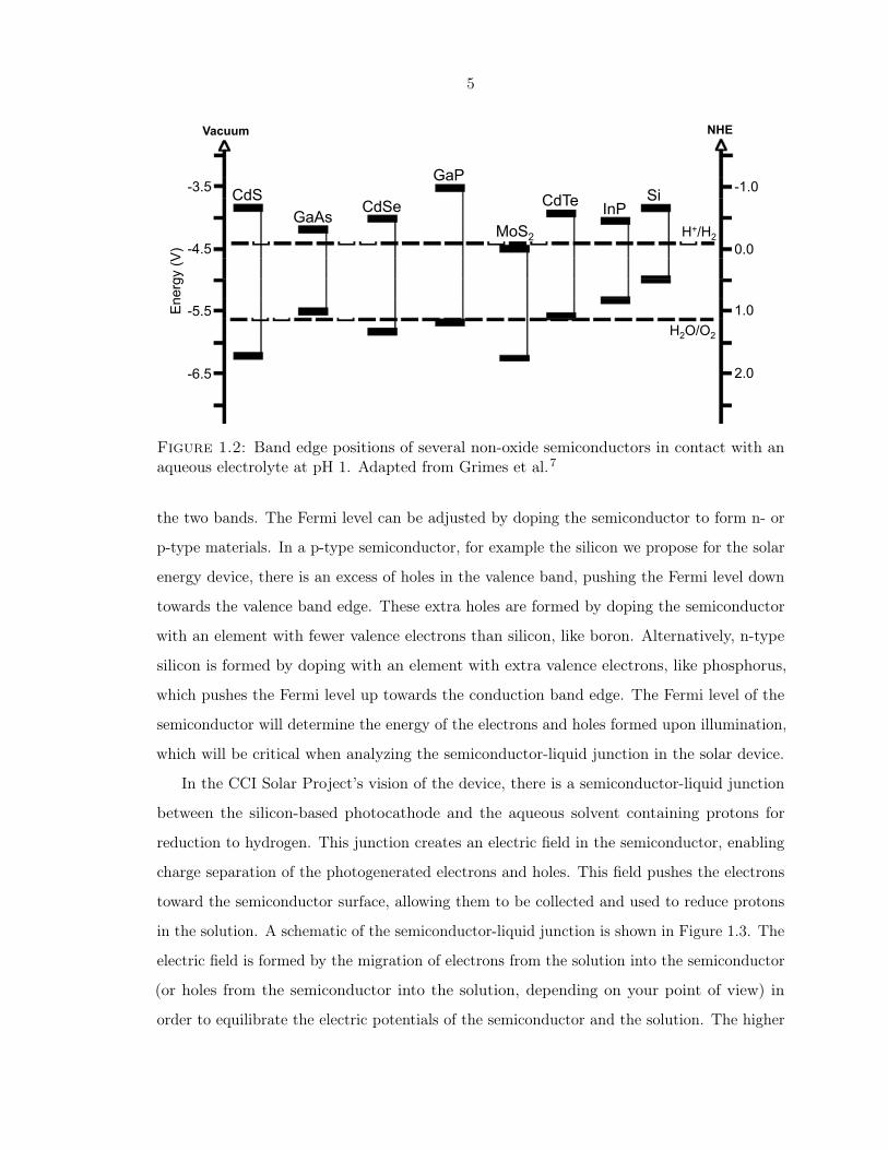
in Figure 1.2 as a comparison of the energy levels of several different materials that have
been considered for use as a photocathode. As can be seen in the figure, the silicon band gap
straddles the H+/H2 redox potential, which means that electrons in the conduction band
will have enough energy to reduce protons to hydrogen.7
The Fermi level of a semiconductor is defined as the electrochemical potential of an
electron in the material, or the energy at which the probability of finding an electron is
1/2.5 In an pure, undoped semiconductor at 0K, where the valence band is completely filled
and the conduction band is completely empty, the Fermi level would be halfway between
5
-3.5
-4.5
-5.5
-6.5
-1.0
0.0
1.0
2.0
CdS GaAs
CdSe
GaP
MoS2
CdTe InP Si
H+/H2
H2O/O2
Vacuum NHE
Ene
rgy
(V)
Figure 1.2: Band edge positions of several non-oxide semiconductors in contact with anaqueous electrolyte at pH 1. Adapted from Grimes et al.7
the two bands. The Fermi level can be adjusted by doping the semiconductor to form n- or
p-type materials. In a p-type semiconductor, for example the silicon we propose for the solar
energy device, there is an excess of holes in the valence band, pushing the Fermi level down
towards the valence band edge. These extra holes are formed by doping the semiconductor
with an element with fewer valence electrons than silicon, like boron. Alternatively, n-type
silicon is formed by doping with an element with extra valence electrons, like phosphorus,
which pushes the Fermi level up towards the conduction band edge. The Fermi level of the
semiconductor will determine the energy of the electrons and holes formed upon illumination,
which will be critical when analyzing the semiconductor-liquid junction in the solar device.
In the CCI Solar Project’s vision of the device, there is a semiconductor-liquid junction
between the silicon-based photocathode and the aqueous solvent containing protons for
reduction to hydrogen. This junction creates an electric field in the semiconductor, enabling
charge separation of the photogenerated electrons and holes. This field pushes the electrons
toward the semiconductor surface, allowing them to be collected and used to reduce protons
in the solution. A schematic of the semiconductor-liquid junction is shown in Figure 1.3. The
electric field is formed by the migration of electrons from the solution into the semiconductor
(or holes from the semiconductor into the solution, depending on your point of view) in
order to equilibrate the electric potentials of the semiconductor and the solution. The higher

6
Ene
rgy
Semiconductor Solution
Depletion width
Helmholtz Layer
ECB
EVB
EF ES +
-
Figure 1.3: p-Type semiconductor-liquid junction. ECB and EVB indicate the energy of theconduction and valence bands, respectively. EF indicates the Fermi level of the semiconductorand ES indicates the redox potential of the solution, which have equilibrated by chargetransfer. The excess of electrons in the depletion width creates an electric field in thesemiconductor, causing bending of the conduction and valence bands.
relative concentration of charge carriers in the solution dictates that the solution potential
will remain nearly unchanged after the charge transfer, with a build-up of positive charges at
the interface, called the Helmholtz layer. Conversely, the relatively low density of charge
carriers in the semiconductor leads to a region of diffuse negative charge, called the depletion
region. The negative charge build-up in the depletion region gives rise to the electric field,
which causes the band bending that drives the electrons towards the surface, as illustrated
by the curved lines in the figure. Thus, when the semiconductor is illuminated, electron-hole
pairs are generated and then separated by the electric field. If the electrons reach the surface
without recombining with holes, they can be used to reduce the protons in solution to
hydrogen. The electric field also moves the holes toward the semiconductor bulk, where they
can be captured and converted to electrical energy at an electrode, or transferred through
the membrane to the photoanode and used to oxidize water.5
For our purposes then, this semiconductor-liquid junction will determine the efficiency of
charge-carrier collection at the surface. We would like to maximize the number of electrons
that reach the surface and are transferred to a catalyst for hydrogen-formation. Silicon

7
surface functionalization can be used to improve the quality of this junction by extending
the charge-carrier lifetime, controlling the energetics of the electrons at the surface, and
facilitating the transfer of those electrons to a catalyst. Our efforts to modify silicon surfaces
to enable solar fuel generation is the subject of this thesis.
1.3 Silicon Surface Modification
Several methods have been developed to functionalize Si surfaces, primarily by exploiting the
reactivity of a H-terminated Si surface.8–10 The H-terminated Si(111) surface is atomically
flat, which makes it an excellent surface for studying the fundamental chemical properties
and reactivity of silicon. This surface is electronically passivated, implying that it has low
charge-carrier recombination rates at the surface. Surface recombination of charge carriers is
a problem for any device in which the collection of charges at the surface is important, such
as a solar cell. Low surface recombination results in longer charge-carrier lifetimes, making
the charges available for collection by catalysts or redox centers at the surface. Conversely,
high surface recombination means that charge-carriers that do get to the surface are trapped
there and rapidly recombine with holes, making them unavailable for further reactions.
The electronic passivation of the H-terminated surface is fleeting, however, as surface
oxidation under aqueous conditions occurs within minutes, resulting in a decrease in charge-
carrier lifetime.11 This can be seen when measuring the surface recombination velocity (SRV)
of a freshly prepared H-terminated Si(111) surface. The SRV, which is calculated from
the charge-carrier lifetime (measured using microwave conductance spectroscopy; details in
Appendix B.3), is an indirect measure of the surface defect density. Fresh H-terminated silicon
has an SRV of <10 cm s−1, corresponding to a charge-carrier lifetime of >1ms.12 However,
after several hours in air, the SRV increases dramatically, to >1000 cm s−1, corresponding to
a charge-carrier lifetime of <10µs.13
Various methods of surface functionalization have been employed to passivate silicon un-
der aqueous and ambient conditions, including thermal14-, radical15,16-, ultraviolet17,18- and
white light19,20- initiated hydrosilylation processes, as well as metal-catalyzed routes.21 Al-
though synthetically versatile, hydrosilylation leaves a significant fraction of unfunctionalized
sites on the Si surface due to the steric bulk of the functional groups. The unfunctionalized
Si sites, which typically consist of residual Si−H bonds, are easily oxidized and therefore

8
result in non-ideally terminated surfaces that exhibit undesirable chemical, electrochemical,
and electrical properties.
Complete termination of Si(111) atop sites by carbon bonds is therefore desirable, and
can be achieved by use of a two-step halogenation/alkylation procedure.11,22–25 In this
method, H-terminated Si surfaces are first halogenated and then reacted with an alkyl-
Grignard or alkyl-Li reagent to yield an alkylated Si surface. Methyl Grignard can be
used via this process to functionalize the surface with methyl groups, which are the only
saturated alkyl groups small enough to be capable of terminating essentially 100% of the
atop sites on an unreconstructed Si(111) surface.26,27 Hydrosilylation, on the other hand,
cannot be used to methylate a silicon surface. This complete termination of the silicon
atop sites can be seen in an STM image of a methyl-terminated silicon surface, shown in
Figure 1.4.28 Methyl-terminated Si surfaces are well passivated against oxidation in air,29
and exhibit low SRVs even after weeks of exposure to ambient atmospheric conditions.30
In addition, CH3−Si(111) surfaces have a low density of mid-gap states, as revealed by
scanning tunneling spectroscopy,26 and exhibit resistance to oxidation in electrochemical and
photoelectrochemical cell applications.29,30
While methyl-terminated silicon has some excellent photoelectrochemical properties, it
is not ideal for use in a water-splitting solar device. Silicon is a poor catalyst for proton
reduction and will require an efficient hydrogen-evolution catalyst to do the actual proton-
reduction reaction on the surface. This catalyst would ideally be tethered to the surface
to minimize catalyst loading in the device and maximize electron-transfer kinetics to the
catalyst from the silicon. In addition, the methyl group on the silicon surface results in a
negative shift in the interfacial dipole. For p-type silicon, this increases the ohmic behavior
of CH3−Si(111) relative to H−Si(111), resulting in lower photovoltages being measured on
the methyl-terminated surface than on the H-terminated surface.31 For these reasons, a
methyl-terminated silicon surface, while exhibiting many of the desirable properties for a
photocathode, will require some additional functionality before it can be incorporated into a
water-splitting device.
Further functionalization, to introduce desirable dipoles and/or molecular catalysts, is
limited on CH3−Si(111) surfaces, owing to the lack of controllable reactivity of the terminal
methyl groups. Therefore, other means are necessary to attach catalytic groups to the
surface. The halogenation/alkylation procedure can be used to attach other functional

9
Figure 1.4: STM image of methyl-terminated Si(111) (4.7K, sample bias Vs = −2.5 V,constant current of 0.050 nA). The color range (dark = low; bright = high) is 0.05 nm. Thelow-index planes of this crystal are indicated in the lower right by directional arrows. Thedrawn parallelogram represents the surface unit cell. Superimposed onto the image are four–CH3 group drawings illustrating their position and relative orientation. The distance between–CH3 groups (L–L′) is 0.38 cm. (Inset) STM image (77K) of the same surface. Image size:1 nm× 1 nm. Adapted from Yu et al.28

10
groups directly to the surface, but these groups are generally larger than methyl groups.
Even a two-carbon ethyl chain is too large to allow for complete termination of the surface
by the chemically inert Si−C bonds, leaving unreacted sites on the surface.13 Synthetic
strategies to produce mixed monolayers have therefore been developed to simultaneously
impart stability and functionality to Si(111) surfaces by forming monolayers composed of
both functional and methyl groups.32,33 The mixed monolayers produced by these methods
possess the resistance to oxidation typically observed for methyl-terminated silicon, and
incorporate desired functional species that are covalently bound to surface silicon atoms.
In this work, we will discuss the formation of several new classes of mixed monolayers
on silicon surface and their uses for solar-fuel forming devices. In Chapter 2, we expanded
on the work done using mixed methyl/allyl monolayers as the starting point for secondary
functionalization. We developed and characterized a new class of mixed methyl/butenyl
monolayers on which we performed cross-coupling reactions using the Grubbs’ catalyst.
The surfaces formed by this method were electroactive and had excellent photoelectronic
properties. In Chapter 3, we developed a new method for forming mixed monolayers on silicon
by combining different modes of reactivity. We showed that the mixed methyl/vinylferrocenyl
monolayers formed using this new method had high electroactive surface coverage, low SRVs,
and resistance to oxidation in air. In addition, these surfaces displayed rapid charge transfer
to the surface-attached redox couple and generated photovoltages of 400mV. In Chapter 4,
we expanded the scope the reaction developed in Chapter 3 to form a new class of mixed
methyl/bipyridyl monolayers that were used as the starting point for the development of
surface-attached hydrogen-evolution catalysts for solar fuel formation. We showed that
these complexes could be assembled on the surface by a variety of spectroscopic techniques,
and that the resultant structures were electroactive and catalytic under acidic conditions.
In Chapter 5, possible mechanisms for the new reaction developed in Chapters 3 and 4
were discussed. Portions of the preceding chapter have been adapted with permission from
Lattimer et al.34 Copyright 2013 American Chemical Society.

11
Chapter 2
Cross Metathesis Reactions on SiliconSurfaces using the Grubbs’ Catalyst,2nd Generation
2.1 Introduction
Carbon-carbon bond formation can be an important tool for the covalent attachment of func-
tional groups to silicon surfaces. Cross-metathesis of two terminal olefins is a well-established
method for the formation of new C−C bonds.35,36 Terminal olefins can be prepared on silicon
surfaces by reacting vinyl or allyl Grignard reagents with chlorine or bromine terminated
silicon surfaces. These surfaces have been prepared and characterized by Plass et al.37 and
O’Leary et al.32 Some work has indicated that surface-terminal olefins are reactive with termi-
nal olefins, via a cross-metathesis reaction using the Grubbs’ catalyst.38,39 The Grubbs’ cata-
lyst, 1st generation (G1), is more formally known as Bis(tricyclohexylphosphine)benzylidine
ruthenium(IV) dichloride (Figure 2.1-G1). Initial experiments used this catalyst as a cross-
coupling agent to react the allyl-terminated Si(111) surface with 4-fluorostyrene, a terminal
aryl olefin. The fluorine acts as a spectroscopic tag to measure the efficacy of the reaction.37
Methyl-terminated Si(111) was used as a control surface to ensure that non-specific binding
did not occur. This work suggested that G1 could be used as a cross-coupling agent to
covalently attach fluorostyrene selectively to allyl-terminated silicon surfaces.
12
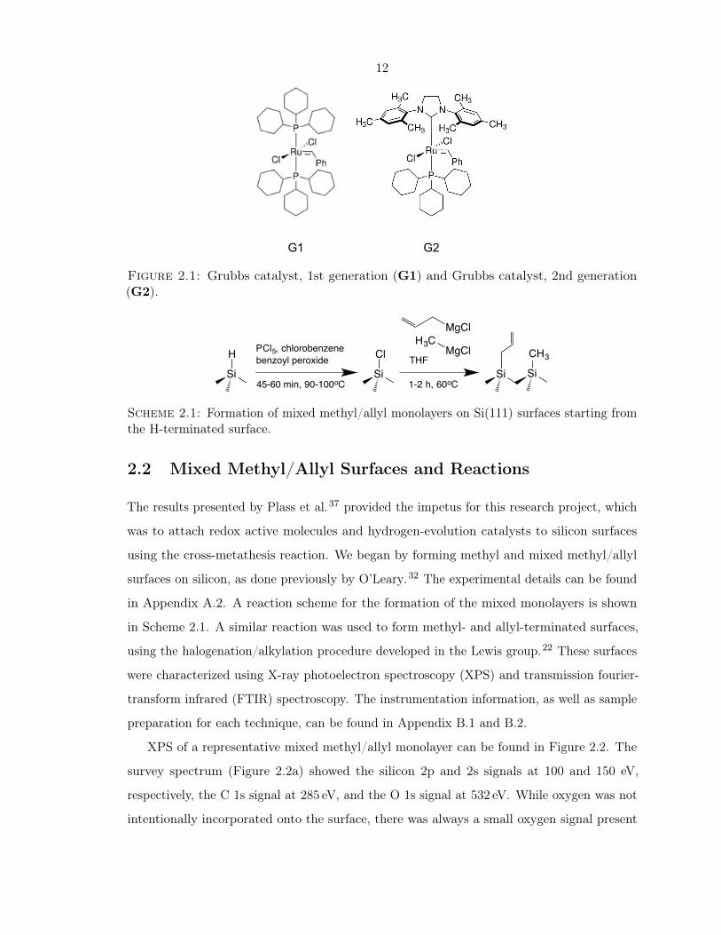
G1 G2
Figure 2.1: Grubbs catalyst, 1st generation (G1) and Grubbs catalyst, 2nd generation(G2).
THF
1-2 h, 60oC
CH3
SiCl
Si Si
H
Si
PCl5, chlorobenzenebenzoyl peroxide
45-60 min, 90-100oC
MgClH3C MgCl
Scheme 2.1: Formation of mixed methyl/allyl monolayers on Si(111) surfaces starting fromthe H-terminated surface.
2.2 Mixed Methyl/Allyl Surfaces and Reactions
The results presented by Plass et al.37 provided the impetus for this research project, which
was to attach redox active molecules and hydrogen-evolution catalysts to silicon surfaces
using the cross-metathesis reaction. We began by forming methyl and mixed methyl/allyl
surfaces on silicon, as done previously by O’Leary.32 The experimental details can be found
in Appendix A.2. A reaction scheme for the formation of the mixed monolayers is shown
in Scheme 2.1. A similar reaction was used to form methyl- and allyl-terminated surfaces,
using the halogenation/alkylation procedure developed in the Lewis group.22 These surfaces
were characterized using X-ray photoelectron spectroscopy (XPS) and transmission fourier-
transform infrared (FTIR) spectroscopy. The instrumentation information, as well as sample
preparation for each technique, can be found in Appendix B.1 and B.2.
XPS of a representative mixed methyl/allyl monolayer can be found in Figure 2.2. The
survey spectrum (Figure 2.2a) showed the silicon 2p and 2s signals at 100 and 150 eV,
respectively, the C 1s signal at 285 eV, and the O 1s signal at 532 eV. While oxygen was not
intentionally incorporated onto the surface, there was always a small oxygen signal present

13
0 200 400 600 800 1000
Cou
nts
Binding Energy (eV)
97 101 105
Cou
nts
Binding Energy (eV) 281 285 289
Cou
nts
Binding Energy (eV)
Si 2p C 1s
Si 2p Si 2s
C 1s
O 1s
a
b c
Figure 2.2: XPS of a mixed methyl/allyl surface. a) Survey spectrum, with the Si 2p, Si 2s,C 1s, and O 1s peaks labeled. b) High-resolution C 1s peak, showing the three componentsof the signal. The lowest energy peak, at 284 eV, was from the carbon directly bound tosilicon. The peak at 285 eV was from the allylic carbons as well as adventitiously adsorbedhydrocarbons. The highest energy peak at 287 eV was from adventitiously adsorbed CO andCO2. c) High-resolution Si 2p peak, with the doublet shown. There was no peak at 103 eV,indicating that the surface was not oxidized during the formation of this mixed monolayer.
due to adventitiously adsorbed water and CO2 from the air onto the surface. High-resolution
spectra of the C 1s and Si 2p peaks are found in Figure 2.2b and c, respectively. The Si 2p
signal consisted of a doublet of peaks at 99 and 100 eV, with an area ratio of 2:1. When
the silicon surface was oxidized, a Si−O peak appeared between 102 and 104 eV.40 The
high-resolution Si 2p XPS signal (Figure 2.2c) showed that there was little to no surface
oxidation present on these mixed monolayers. The C 1s XPS signal (Figure 2.2b) consisted
of three peaks, at 284, 285, and 287 eV. These corresponded to carbon directly bound to
silicon at 284 eV,13,29 carbon bound to carbon or hydrogen at 285 eV, and carbon bound to
more electronegative elements like oxygen at 287 eV. The peak at 287 eV was ascribed to
adventitiously adsorbed species like CO and CO2, while the peak at 285 eV resulted from a
combination of the allyl carbons on the surface and adventitiously adsorbed species like CH4
and higher-order hydrocarbons. These species were present in small quantities even under
ultra high vacuum conditions from the atmosphere of the lab or from residual pump oil in
the instrument.
14
Hydride
Methyl
Allyl
Mixed Methyl/Allyl
Si-H
Si-H
Si-O
CH
3
CH
3
C=C
CO
2
C-H
12
Abs
orba
nce
(mA
u)
8
4
0 3,500 2,500 1,500 500
Wavenumbers (cm-1)
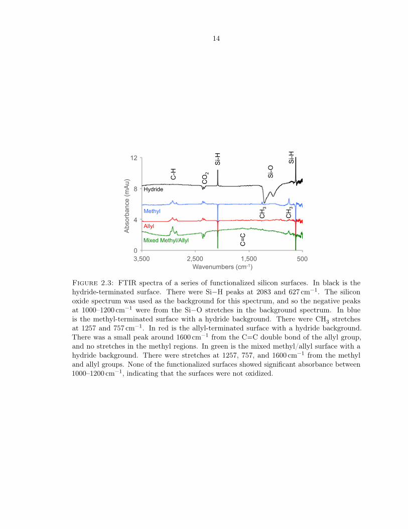
Figure 2.3: FTIR spectra of a series of functionalized silicon surfaces. In black is thehydride-terminated surface. There were Si−H peaks at 2083 and 627 cm−1. The siliconoxide spectrum was used as the background for this spectrum, and so the negative peaksat 1000–1200 cm−1 were from the Si−O stretches in the background spectrum. In blueis the methyl-terminated surface with a hydride background. There were CH3 stretchesat 1257 and 757 cm−1. In red is the allyl-terminated surface with a hydride background.There was a small peak around 1600 cm−1 from the C−−C double bond of the allyl group,and no stretches in the methyl regions. In green is the mixed methyl/allyl surface with ahydride background. There were stretches at 1257, 757, and 1600 cm−1 from the methyland allyl groups. None of the functionalized surfaces showed significant absorbance between1000–1200 cm−1, indicating that the surfaces were not oxidized.

15
These surfaces were further characterized by transmission Fourier-transform infrared
spectroscopy (FTIR), shown in Figure 2.3. First, the surface was cleaned with piranha (1 : 2
v/v 10.1 M hydrogen peroxide (H2O2, aq) : 18 M sulfuric acid (H2SO4)), resulting in a thin
silicon oxide layer on the silicon wafer. An FTIR spectrum of this surface was collected
and used as the background for subsequent spectra. Next, the surface was etched with HF
and NH4F, resulting in atomically flat H-terminated silicon. An FTIR spectrum of this
surface with the oxide surface as a background is shown in Figure 2.3. The characteristic
Si−H stretches at 2083 and 627 cm−1 were clearly visible, as are the negative Si−O peaks
at 1224 and 1058 cm−1.41 This demonstrates that the surface had lost all Si−O bonds,
which were replaced by Si−H bonds. After functionalization of the Si−H surface to form
a methyl-terminated surface, a mixed methyl/allyl surface, or an allyl-terminated surface,
more FTIR spectra were collected, as shown in Figure 2.3. The hydride-terminated surface
was used for background subtraction in these spectra.
The experimental details for the preparation of these surfaces can be found in Appen-
dices A.1, A.2, and A.3. There were peaks from the methyl groups at 1257 and 757 cm−1,41
and a small peak from the terminal olefin of the allyl group at ∼1600 cm−1.37 In addition, a
negative peak at 2083 cm−1 can be seen in the spectra with a hydride background, indicating
that the Si−H bonds have been replaced by Si−C bonds. There was no significant absorp-
tion around 1000–1200 cm−1, indicating that the surface had not been oxidized during the
formation of these monolayers, verifying our Si 2p XPS observations.
A series of surfaces with varying allyl:methyl ratios was formed by varying the amount of
methyl and allyl Grignard in each 1M solution. A series of such surfaces was analyzed using
FTIR spectroscopy, and the results are shown in Figure 2.4. While the methyl peaks at 1257
and 757 cm−1 were fairly well defined, the allylic peak at ∼1600 cm−1 was much harder to
see.
2.2.1 Cross-Coupling Reactions
These mixed methyl/allyl surfaces were then used as the substrate for the cross-coupling
reaction seen by Plass et al.37 using the Grubbs’ catalyst, 2nd generation. This newer catalyst
was used rather than G1 by recommendation from Leslie O’Leary because the 2nd generation
catalyst had shown increased activity under solution conditions. The Grubbs’ catalyst, 2nd
generation (G2, Figure 2.1-G2) is also known as Benzylidene[1,3-bis(2,4,6-trimethylphenyl)-2-

16
-0.010
-0.005
0.000
0.005
580 1080 1580 2080 2580 3080 3580
Abs
orba
nce
(Au)
wavenumber (cm-1)
H2O
CO
2
Si-H
CH
3
CH
3
C-H
C=C
-H
CH
3 S
i-H
Methyl
2% Allyl/98% Methyl
5% Allyl/95% Methyl
10% Allyl/90% Methyl
Allyl
Figure 2.4: Surface transmission FTIR spectra of a series of mixed methyl/allyl functional-ized silicon surfaces. Each spectra is labeled by the formulation of the 1M Grignard solutionused to functionalize the surface. The surfaces containing methyl groups had peaks at 1257and 757 cm−1, while the surfaces with allyl groups had small absorbances around 1600 cm−1.
imidazolidinylidene]dichloro(tricyclohexylphosphine)ruthenium. The reaction was performed
in an Ar-filled glove box, and was done by placing the functionalized silicon wafer in a
solution of 1M catalyst in dichloromethane (CH2Cl2) at 50C overnight. The wafer was then
rinsed with CH2Cl2 and placed under 4-fluorostyrene at 50 C for 12–24 additional hours.
After the reaction, the wafer was rinsed with CH2Cl2, and cleaned by sequential sonication
in CH2Cl2, CH3OH, and water before analysis by XPS. However, none of the many surfaces
exposed to these conditions displayed any fluorine signal in XPS.
After observing these disappointing results, we tried to replicate the results seen by Plass
et al.37 using allyl surfaces for the cross-coupling reaction, and methyl-terminated silicon as
the control surface. In addition, the control reaction without using the Grubbs’ catalyst was
done. The results are shown in Figure 2.5. From the F 1s XPS signals on these four surfaces,
it was clear that the cross-coupling reaction did not proceed as expected. Surface coverages
of fluorostyrene on these surfaces were quantified based on the F 1s and Si 2p XPS signals,
as described in Appendix B.1.1. On the methyl surface exposed to G2 and 4-fluorostyrene
(4-FS), the surface coverage of 4-FS on the surface was 0.04± 0.05 monolayers. For the
methyl surface exposed only to 4-FS, the surface coverage was 0.03± 0.05. These values
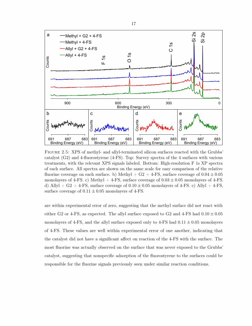
17
0 300 600 900
Cou
nts
Binding Energy (eV)
Methyl + G2 + F Methyl + F Allyl + G2 + F Allyl + F
O 1
s C 1
s Si 2
s
Si 2
p
F 1s
683 687 691
Cou
nts
Binding Energy (eV) 683 687 691
Cou
nts
Binding Energy (eV) 683 687 691
Cou
nts
Binding Energy (eV)
e
683 687 691
Cou
nts
Binding Energy (eV)
a
b c d
Methyl + G2 + 4-FS Methyl + 4-FS Allyl + G2 + 4-FS Allyl + 4-FS
Figure 2.5: XPS of methyl- and allyl-terminated silicon surfaces reacted with the Grubbs’catalyst (G2) and 4-fluorostyrene (4-FS). Top: Survey spectra of the 4 surfaces with varioustreatments, with the relevant XPS signals labeled. Bottom: High-resolution F 1s XP spectraof each surface. All spectra are shown on the same scale for easy comparison of the relativefluorine coverage on each surface. b) Methyl + G2 + 4-FS, surface coverage of 0.04± 0.05monolayers of 4-FS. c) Methyl + 4-FS, surface coverage of 0.03± 0.05 monolayers of 4-FS.d) Allyl + G2 + 4-FS, surface coverage of 0.10± 0.05 monolayers of 4-FS. e) Allyl + 4-FS,surface coverage of 0.11± 0.05 monolayers of 4-FS.
are within experimental error of zero, suggesting that the methyl surface did not react with
either G2 or 4-FS, as expected. The allyl surface exposed to G2 and 4-FS had 0.10± 0.05
monolayers of 4-FS, and the allyl surface exposed only to 4-FS had 0.11± 0.05 monolayers
of 4-FS. These values are well within experimental error of one another, indicating that
the catalyst did not have a significant affect on reaction of the 4-FS with the surface. The
most fluorine was actually observed on the surface that was never exposed to the Grubbs’
catalyst, suggesting that nonspecific adsorption of the fluorostyrene to the surfaces could be
responsible for the fluorine signals previously seen under similar reaction conditions.

18
2.2.2 Bromination Reactions
At this point, we determined that endeavoring to reproduce the results from Plass et al.37 was
not a constructive use of time, and instead began to explore other methods to characterize
the mixed methyl/allyl surfaces. Bromination of the allyic groups on the surface could help to
differentiate between the allyl and methyl groups, and thus better enable the quantification of
the various components of the mixed monolayers. Knowledge of how much of each species is
actually on the mixed monolayer surfaces could help explain why the cross coupling reactions
do not appear to proceed as expected.
Silicon-attached terminal alkenes have been brominated previously using Br2.42 Alkene
bromination has been demonstrated to occur using a dilute solution of Br2 in methanol,43
and so we used this method for the bromination of the mixed methyl/alkyl monolayers.
Bromination of a series of surfaces was done by immersing the prepared surface in a 5%
solution of Br2 in anhydrous methanol in a N2-purged flush box; this is a glove box with a
constant flow of N2 to maintain an inert atmosphere, or an O2 and H2O-free environment. This
was done to minimize oxidation of the surface and to control the bromination reaction. The
experimental details of the bromination reaction can be found in Appendix A.4. Hydrogen-
terminated silicon was used as a control surface look at silicon-bromine reactivity, and to
study the Br 3d peak at 70 eV in XPS to see how bromine bonded to silicon would appear.
While reaction between the Br2 and methyl groups was expected to be minimal, reaction
of unfunctionalized silicon sites in the mixed monolayer with Br2 was likely. Distinguishing
between the bromine bound to silicon (Br−Si) and bromine bound to carbon (Br−C) signals
via XPS was thus critical to these experiments.
Figure 2.6 shows the high-resolution Br 3d XPS signals from a series of silicon surfaces
reacted with 5% Br2 in methanol (v/v) for 5min, with normalized counts for ease of com-
parison. There were clearly two sets of doublets within the peaks, most likely corresponding
to Br−Si (blue) and Br−C (red), though residual Br2 from the reaction cannot be ruled out
completely, despite the low probability of any remaining on the surfaces after the rigorous
sonication and rinsing to which the surfaces were all exposed during the cleaning procedure,
as well as the ultra high vacuum atmosphere of the XPS chamber. The brominated Si−H
surface is shown in Figure 2.6a, and the dominant peaks in this Br 3d spectrum were at
69 and 70 eV, in the 3:2 ratio expected for a d-type XPS signal. Thus we assigned the

19
65 70 75
Cou
nts
Binding Energy (eV)
SI-H
66 70 74
Cou
nts
Binding Energy (eV)
5% Allyl/Methyl
66 70 74 C
ount
s
Binding Energy (eV)
10% Allyl/Methyl
66 70 74
Cou
nts
Binding Energy (eV)
Allyl
a b c
d e f
66 70 74
Cou
nts
Binding Energy (eV)
Methyl
66 70 74
Cou
nts
Binding Energy (eV)
2% Allyl/Methyl b c
Figure 2.6: High-resolution Br 3d XPS of a series of silicon surfaces exposed to Br2 inmethanol for 5min. The counts in all panels are normalized for ease of comparison, with thedoublet corresponding to Br−Si in blue and the doublet corresponding to Br−C in red. a)H-terminated silicon had a large doublet at 69 and 70 eV, indicating that the surface washighly susceptible to attack by Br2 to form Si−Br. b) Methyl-terminated silicon showed verylittle reaction with the Br2, as expected. c,d,e) Mixed monolayers formed with 2, 5, and 10%allyl Grignard in 1M Grignard reaction solutions, with the remainder made up by methylGrignard. Increasing allyl concentration lead to increased surface coverage of bromine boundto both silicon and carbon. f) Allyl-terminated silicon had two doublets, at 69/70 eV fromBr−Si, and 70/71 eV from Br−C due to bromination of the allylic group.
doublet at 69/70 eV to be the one arising from bromine bound to the silicon surface, or
Br−Si. The methyl-terminated surface exposed to Br2 (Figure 2.6b) shows very little Br
3d signal, as expected, corresponding to 0.01± 0.01 monolayers. Details of the monolayer
coverage calculations can be found in Appendix B.1.1.
Mixed methyl/allyl surfaces formed by varying the relative ratios of methyl and allyl
Grignard in the reaction solution were prepared and then reacted with Br2 in methanol, with
the results shown in Figure 2.6c-e. These surfaces showed increasing amounts of bromination
as the allyl Grignard concentration in the reaction solution was increased. This suggested
that by increasing the allyl Grignard concentration of the reaction solution, more allyl groups
were incorporated into the mixed monolayer, as had been shown previously by O’Leary et
al.32 The increased allyl concentration on the surface then lead to higher levels of bromination
of those surfaces. However, both the Br−Si and Br−C components of the Br 3d peak seemed

20
C−Sia C−Sib Br−Cb Br−SibMethyl 1.00 0.97 0.02 0.01
2% Allyl 0.90 0.94 0.04 0.065% Allyl 0.82 0.66 0.11 0.1410% Allyl 0.73 0.65 0.13 0.11
100% Allyl 0.70 0.64 0.25 0.16aSurface as prepared.bSurface after reaction with Br2 in methanol.
Table 2.1: Surface coverage in monolayers of carbon and bromine on various silicon surfacesfunctionalized with varying amounts of methyl and allyl groups. The error in all reportednumbers is ±0.1. C−Si was calculated using the C 1s peak at 284 eV corresponding to surface-bound carbon. Br−C was calculated using the Br 3d doublet at 70 and 71 eV, correspondingto the bromine bound to carbon. Br−Si was calculated using the Br 3d doublet at 69 and70 eV, corresponding to the bromine bound to the silicon surface.
to be increasing, suggesting that the silicon surface had become more susceptible to attack
by the Br2 than in the case for the methyl-terminated surface, probably because the larger
allyl group prevented 100% termination of the silicon atop sites,13 leading to larger numbers
of unfunctionalized sites as the allyl incorporation into the mixed monolayer was increased.
This was supported by the apparent decrease in surface coverage of carbon bound to silicon
on the surface after the bromination reaction. Table 2.1 contains the surface coverage of
selected elements for all samples shown in Figure 2.6.
Finally, an allyl-terminated surface was prepared and reacted with Br2 in methanol,
shown in Figure 2.6f. This surface had the largest Br−C and Br−Si peaks, as expected.
However, this surface had only ∼25% surface coverage of Br−C, which was much lower than
the total amount of allyl-group coverage measured using the C 1s XPS signal. This suggested
that the reaction was incomplete or that the sterics of the allyl-terminated surface did not
allow for all the allyl groups to react with the Br2. However, the large amount of Br−Si seen
on this and the mixed surfaces suggested that increasing the reaction time could result in
damage to the mixed monolayer by reaction of the Br2 with the silicon surface.
We tested the stability of the surfaces to Br2 over time by exposing methyl-, allyl-, and
mixed monolayer-terminated surfaces to the Br2 in methanol solution for 0–60min. The
methyl surface was quite stable to bromination, with effectively no loss of the C−Si peak and
very low (0.01± 0.01 monolayers) bromination of the surface after 60min in a 5% Br2 in
methanol (v/v) solution. Thus we concluded that the silicon-methyl bond was not particularly
reactive with Br2. The allyl surface showed immediate reactivity with Br2, and after 60min

21
did not change significantly. The C−Si and Br−C coverages were nearly identical, and
hovered around 0.5± 0.1 monolayers from 2–60min exposure to Br2 in methanol, indicating
that the allyl group reacted quickly. The Br-Si coverage also remained fairly constant, around
0.20± 0.05 monolayers, indicating that both the unreacted silicon atop sites and some Si−C
bonds reacted with Br2. However, this reaction appeared self-limiting, which was indicative
of the stability of the allyl surface. On a mixed monolayer made from a 2% allyl and 98%
methyl Grignard solution (2% allyl surface), the reaction also proceeded rapidly, with little
change to the surface from 2–60min of exposure to Br2 in methanol. The C−Si coverage
dropped from 0.9± 0.1 to 0.7± 0.1 monolayers over the hour, with a concomitant increase
in Br−Si to 0.10± 0.05 monolayers. The Br−C coverage also stayed fairly constant around
0.08± 0.10 monolayers. This suggested that allyl coverage was quite low, but previous
studies using 2% allyl surfaces indicated that allyl coverage is closer to 0.4 monolayers.32
From these results, it appeared that there was an olefin on the surface that was available
to react, at least with Br2. However, the allylic concentration on the 2% allyl surface may
have been much lower than initial estimates. Based on these results, the absence of reactivity
of the allyl surface with G2 could have been a steric problem. To test this hypothesis, we
studied how longer-chain olefins reacted on the surface.
2.3 Mixed Butenyl/Methyl Surfaces
The 4-carbon chain terminal olefin, or butenyl Grignard, was used to form mixed monolayers
with methyl Grignard. This reagent was chosen because it had an additional carbene
group extending the olefin from the surface, and was also commercially available. Mixed
butenyl/methyl surfaces were formed by mixing the Grignard reagents in various ratios
in solution to form a 1M Grignard solution and allowing the chlorine-terminated silicon
wafers to react for 1–2 h at 65 C. The experimental details can be found in Appendix A.5.
These mixed monolayers were characterized using XPS, FTIR, and microwave conductance
spectroscopy to measure surface recombination velocity (SRV). The experimental details for
these techniques can be found in Appendices B.1, B.2, and B.3.
XPS was used to determine the total carbon surface coverage on these surfaces. Figure 2.7
shows the C−Si coverage of a series of mixed monolayers formed by varying the ratio of
butenyl and methyl Grignards in the reaction mixure. These surfaces were functionalized in

22
0.5
0.6
0.7
0.8
0.9
1
0 20 40 60 80 100
Sur
face
Cov
erag
e (m
onol
ayer
s)
Percent butenyl Grignard in reaction solution
Figure 2.7: Plot of total surface coverage as measured using the C−Si peak from the C 1sXPS data collected on a series of mixed monolayers on silicon formed by varying the ratioof methyl to butenyl Grignard in solution. Dashed line shown as guide for the eye. Totalsurface coverage decreased nonlinearly from 1.0± 0.1 monolayers to 0.6± 0.1 monolayers asthe butenyl Grignard concentration in solution increased from 0 to 100%.
solutions with butenyl Grignard concentrations ranging from 0–100% in solution, hereafter
referred to as X%ButMM, where X is the percentage of butenyl Grignard in the reaction
solution. The remainder of the solution comprised methyl Grignard, for a final concentration
of 1M Grignard in THF. The high-resolution C 1s XPS was composed of both the methyl
and butenyl groups of the mixed monolayers and therefore the quantification of the relative
amounts of each component could not be determined by XPS. The surface oxidation could
be measured using the high-resolution Si 2p XPS regions of each surface, and the absence
of any surface oxide peak at 103 eV was used to ensure high quality surfaces for subsequent
reactivity.
FTIR spectra of a series of mixed monolayers containing various amounts of methyl and
butenyl Grignard in the reaction solution were analyzed to look for the terminal olefin peak
at ∼1600 cm−1, as well as the methyl peaks at 1257 and 757 cm−1. These spectra are shown
in Figure 2.8. All four surfaces had distinct signals at 1257 and 757 cm−1, indicating that all
four surfaces had methyl groups on the surface, as expected. While there was some indication
of the C−−C stretch in the spectrum of the 15%ButMM surface, it was small and difficult
to distinguish. There was very little surface oxidation based on the absence of a significant
absorbance around 1000 to 1200 cm−1 on all the surfaces. This agreed well with the XPS
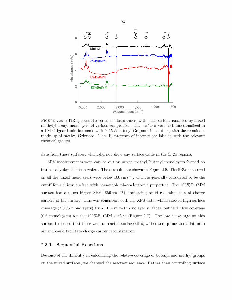
23
0.000
0.002
0.004
0.006
0.008
500 1000 1500 2000 2500 3000
8
Abs
orba
nce
(mA
u) 6
4
0 2,500 1,500 500
Wavenumbers (cm-1) C
O2
Si-H
CH
3
CH
3
C-H
C=C
-H
CH
3 S
i-H
2
3,000 2,000 1,000
Methyl
2%ButMM
5%ButMM
15%ButMM
Figure 2.8: FTIR spectra of a series of silicon wafers with surfaces functionalized by mixedmethyl/butenyl monolayers of various composition. The surfaces were each functionalized ina 1M Grignard solution made with 0–15% butenyl Grignard in solution, with the remaindermade up of methyl Grignard. The IR stretches of interest are labeled with the relevantchemical groups.
data from these surfaces, which did not show any surface oxide in the Si 2p regions.
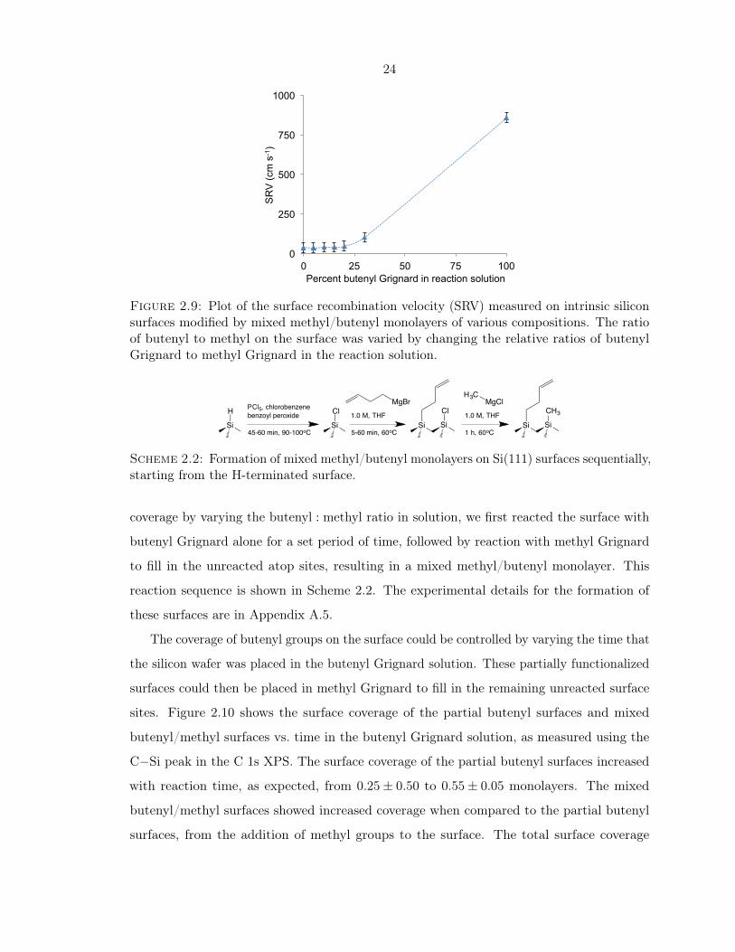
SRV measurements were carried out on mixed methyl/butenyl monolayers formed on
intrinsically doped silicon wafers. These results are shown in Figure 2.9. The SRVs measured
on all the mixed monolayers were below 100 cm s−1, which is generally considered to be the
cutoff for a silicon surface with reasonable photoelectronic properties. The 100%ButMM
surface had a much higher SRV (850 cm s−1), indicating rapid recombination of charge
carriers at the surface. This was consistent with the XPS data, which showed high surface
coverage (>0.75 monolayers) for all the mixed monolayer surfaces, but fairly low coverage
(0.6 monolayers) for the 100%ButMM surface (Figure 2.7). The lower coverage on this
surface indicated that there were unreacted surface sites, which were prone to oxidation in
air and could facilitate charge carrier recombination.
2.3.1 Sequential Reactions
Because of the difficulty in calculating the relative coverage of butenyl and methyl groups
on the mixed surfaces, we changed the reaction sequence. Rather than controlling surface
24
0
250
500
750
1000
0 25 50 75 100 Percent butenyl Grignard in reaction solution
SR
V (c
m s
-1)
Figure 2.9: Plot of the surface recombination velocity (SRV) measured on intrinsic siliconsurfaces modified by mixed methyl/butenyl monolayers of various compositions. The ratioof butenyl to methyl on the surface was varied by changing the relative ratios of butenylGrignard to methyl Grignard in the reaction solution.
1.0 M, THF
5-60 min, 60oC
Cl
SiCl
Si Si
H
Si
PCl5, chlorobenzenebenzoyl peroxide
45-60 min, 90-100oC
MgBr1.0 M, THF
1 h, 60oC
H3C MgClCH3
SiSi
Scheme 2.2: Formation of mixed methyl/butenyl monolayers on Si(111) surfaces sequentially,starting from the H-terminated surface.
coverage by varying the butenyl : methyl ratio in solution, we first reacted the surface with
butenyl Grignard alone for a set period of time, followed by reaction with methyl Grignard
to fill in the unreacted atop sites, resulting in a mixed methyl/butenyl monolayer. This
reaction sequence is shown in Scheme 2.2. The experimental details for the formation of
these surfaces are in Appendix A.5.
The coverage of butenyl groups on the surface could be controlled by varying the time that
the silicon wafer was placed in the butenyl Grignard solution. These partially functionalized
surfaces could then be placed in methyl Grignard to fill in the remaining unreacted surface
sites. Figure 2.10 shows the surface coverage of the partial butenyl surfaces and mixed
butenyl/methyl surfaces vs. time in the butenyl Grignard solution, as measured using the
C−Si peak in the C 1s XPS. The surface coverage of the partial butenyl surfaces increased
with reaction time, as expected, from 0.25± 0.50 to 0.55± 0.05 monolayers. The mixed
butenyl/methyl surfaces showed increased coverage when compared to the partial butenyl
surfaces, from the addition of methyl groups to the surface. The total surface coverage
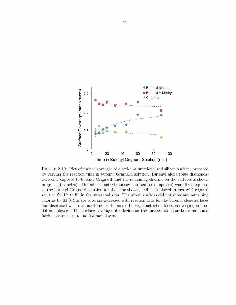
25
0
0.3
0.6
0.9
0 20 40 60 80 100
Sur
face
Cov
erag
e (m
onol
ayer
s)
Time in Butenyl Grignard Solution (min)
Butenyl alone Butenyl + Methyl Chlorine
Figure 2.10: Plot of surface coverage of a series of functionalized silicon surfaces preparedby varying the reaction time in butenyl Grignard solution. Butenyl alone (blue diamonds)were only exposed to butenyl Grignard, and the remaining chlorine on the surfaces is shownin green (triangles). The mixed methyl/butenyl surfaces (red squares) were first exposedto the butenyl Grignard solution for the time shown, and then placed in methyl Grignardsolution for 1 h to fill in the unreacted sites. The mixed surfaces did not show any remainingchlorine by XPS. Surface coverage increased with reaction time for the butenyl alone surfacesand decreased with reaction time for the mixed butenyl/methyl surfaces, converging around0.6 monolayers. The surface coverage of chlorine on the butenyl alone surfaces remainedfairly constant at around 0.3 monolayers.

26
decreased with reaction time in butenyl Grignard, however, from 0.80± 0.05 to 0.60± 0.05
monolayers. This suggested that with high enough butenyl coverage, there were some surface
sites that could not be functionalized by the methyl group, probably for steric reasons. The
remaining chlorine on the partial butenyl surfaces, as measured using the Cl 2s XPS signal, is
also shown in Figure 2.10. The surface coverage of chlorine remained fairly constant around
0.30± 0.05 monolayers, though it did decrease slightly with reaction time in butenyl Grignard
solution. The total coverage of butenyl and chlorine on the partial butenyl surfaces did not
add up to 1.0 monolayers, however. This suggested that the chlorine coverage measured by
XPS may have been be influenced by some outside factor which could artificially decrease
the amount of chlorine remaining on the surface, possibly during the cleaning process. The
surfaces were all sonicated in CH3OH prior to analysis by XPS, which could have replaced
some of the chlorine groups on the surface, or the chlorine sites could have reacted with
water or oxygen in the air. After methylation of the partial butenyl surfaces, there was no
measureable Cl 2s signal by XPS, indicating that the methyl Grignard had reacted with the
remaining chlorinated surface sites.
Representative high-resolution XPS of the Si 2p, C 1s, and Cl 2s peaks of a partial butenyl
and a mixed methyl/butenyl surface are shown in Figure 2.11. These surfaces were both
reacted with 1.0M butenyl Grignard at 65 C for 20min. The mixed methyl/butenyl surface
was then reacted with 1.0M methyl Grignard at 65 C for 2 h. The Si 2p region of both
surfaces did not have a silicon oxide peak at 103 eV, indicating that the surfaces were not
oxidized during functionalization. The C 1s region of both surfaces were composed of three
peaks, at 284, 285.5, and 287 eV. The C-Si component at 284 eV was larger for the mixed
methyl/butenyl surface than for the partial butenyl surface, corresponding to 0.78± 0.05 and
0.35± 0.05 monolayers, respectively. This increase in surface coverage suggested that the
methyl Grignard reacted with the chlorine groups remaining on the partial butenyl surface,
resulting in a surface that was composed of both butenyl and methyl groups. The partial
butenyl surface showed a large chlorine signal in the Cl 2s region, at 270 eV, corresponding to
0.30± 0.05 monolayers. The Cl 2s region of the mixed methyl/butenyl surface did not show
any chlorine remaining on the surface, which supported the idea that the methyl Grignard
could react with the remaining chlorine groups on the partial butenyl surface, forming a
mixed monolayer.
The SRVs measured on partial butenyl and mixed methyl/butenyl surfaces are shown in
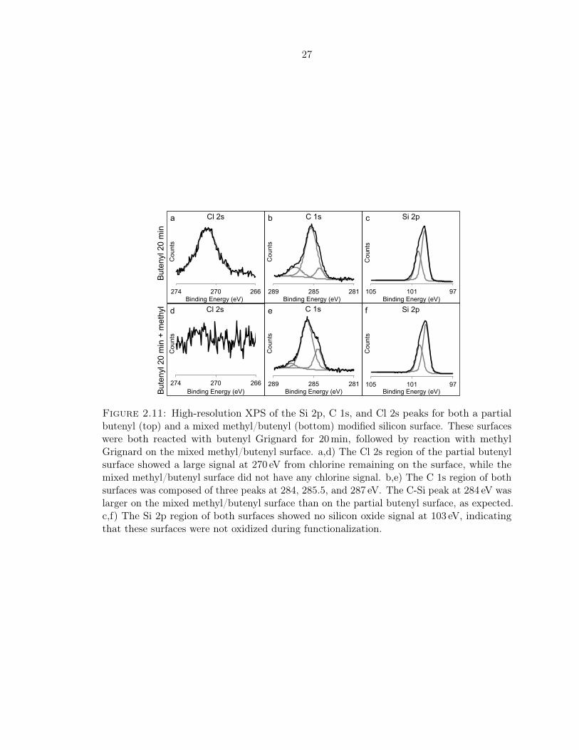
27
281 285 289
Cou
nts
Binding Energy (eV)
C 1s
97 101 105
Cou
nts
Binding Energy (eV)
Si 2p
266 270 274
Cou
nts
Binding Energy (eV)
Cl 2s
281 285 289
Cou
nts
Binding Energy (eV)
C 1s
97 101 105
Cou
nts
Binding Energy (eV)
Si 2p
266 270 274
Cou
nts
Binding Energy (eV)
Cl 2s
a b c
d e f
But
enyl
20
min
B
uten
yl 2
0 m
in +
met
hyl
Figure 2.11: High-resolution XPS of the Si 2p, C 1s, and Cl 2s peaks for both a partialbutenyl (top) and a mixed methyl/butenyl (bottom) modified silicon surface. These surfaceswere both reacted with butenyl Grignard for 20min, followed by reaction with methylGrignard on the mixed methyl/butenyl surface. a,d) The Cl 2s region of the partial butenylsurface showed a large signal at 270 eV from chlorine remaining on the surface, while themixed methyl/butenyl surface did not have any chlorine signal. b,e) The C 1s region of bothsurfaces was composed of three peaks at 284, 285.5, and 287 eV. The C-Si peak at 284 eV waslarger on the mixed methyl/butenyl surface than on the partial butenyl surface, as expected.c,f) The Si 2p region of both surfaces showed no silicon oxide signal at 103 eV, indicatingthat these surfaces were not oxidized during functionalization.

28
0
500
1000
1500
2000
0 20 40 60 80 100
SR
V (c
m s
-1)
Time in Butenyl Grignard solution (min)
without Me
with Me
10
30
50
0 50 100
SR
V (c
m s
-1)
Time in Butenyl Grignard (min)
Figure 2.12: Plot of the SRV vs. time in butenyl Grignard solution measured on a seriesof functionalized silicon surfaces. Shown in blue (squares) are the surfaces that were onlyexposed to butenyl Grignard. In red (diamonds) are the surfaces that were first reacted withbutenyl Grignard solution for the given amount of time, and then placed in methyl Grignardfor 2 h. The inset shows the SRVs of the mixed methyl/butenyl surfaces on an expandedscale for clarity.
Figure 2.12. The surfaces formed by varying the time in butenyl Grignard all had large SRVs,
of >1000 cm s−1, indicating fast charge carrier recombination at the surface, and therefore
poor photoelectronic properties. However, the same treatment with butenyl Grignard followed
by reaction with methyl Grignard resulted in SRVs of <50 cm s−1. These long charge-carrier
lifetimes indicated that charge-carrier recombination at the surface was slow, suggesting
that these surfaces had excellent photoelectronic properties. All of this data indicated that
methylation of the partial butenyl surfaces formed a mixed monolayer of butenyl and methyl
groups on the surface, resulting in surfaces that had high total surface coverage as well as
high coverage of the functional moiety (namely butenyl). These mixed monolayers did not
show any surface oxidation by XPS or FTIR and displayed low SRVs, indicating that they
had good photoelectronic properties.
2.4 Cross-coupling Reactions of Butenyl/Methyl Surfaces
Based on the above data, we have developed a method for forming mixed butenyl/methyl
monolayers on silicon with high coverage of butenyl groups and good photoelectronic proper-
ties. Cross-coupling of functional groups onto the surface using the Grubbs’ 2nd generation
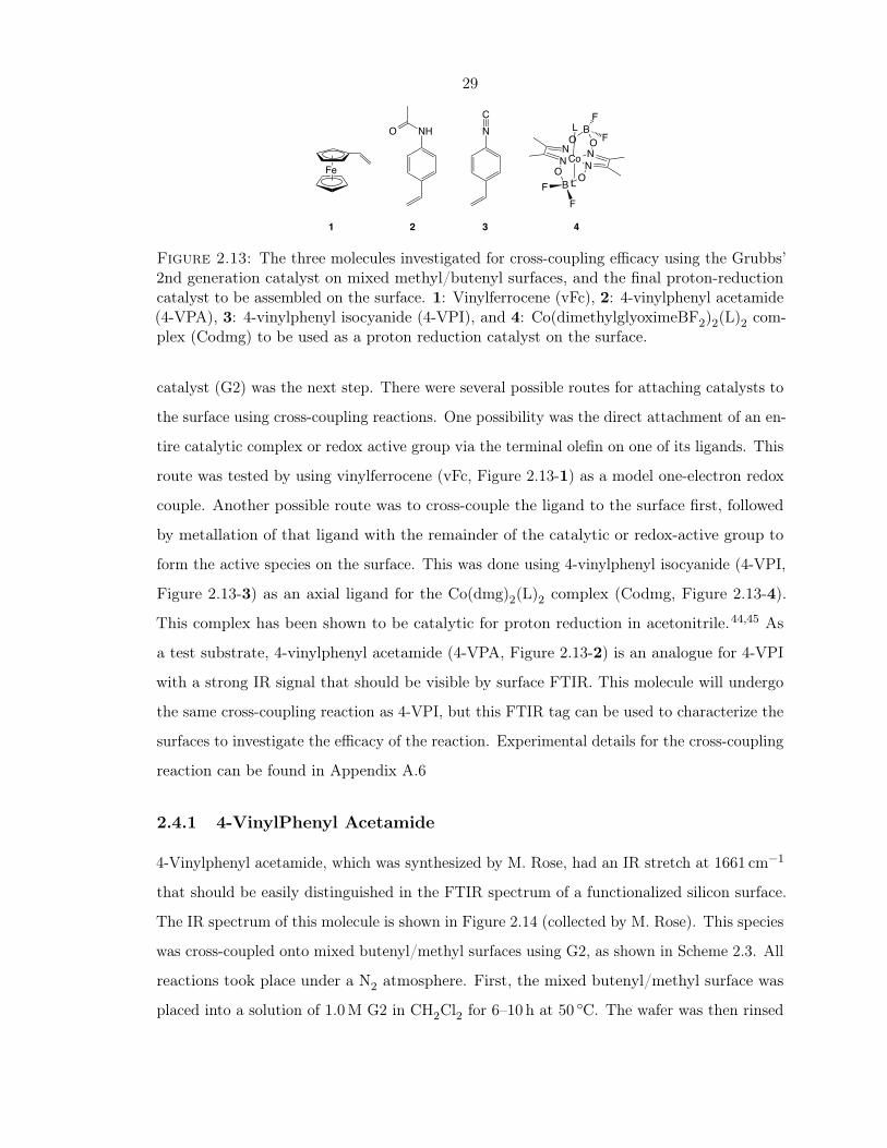
29
LFe
NHO NC
1 2 3 4
CoNN N
NO O
BF
F
OOB
FF
L
Figure 2.13: The three molecules investigated for cross-coupling efficacy using the Grubbs’2nd generation catalyst on mixed methyl/butenyl surfaces, and the final proton-reductioncatalyst to be assembled on the surface. 1: Vinylferrocene (vFc), 2: 4-vinylphenyl acetamide(4-VPA), 3: 4-vinylphenyl isocyanide (4-VPI), and 4: Co(dimethylglyoximeBF2)2(L)2 com-plex (Codmg) to be used as a proton reduction catalyst on the surface.
catalyst (G2) was the next step. There were several possible routes for attaching catalysts to
the surface using cross-coupling reactions. One possibility was the direct attachment of an en-
tire catalytic complex or redox active group via the terminal olefin on one of its ligands. This
route was tested by using vinylferrocene (vFc, Figure 2.13-1) as a model one-electron redox
couple. Another possible route was to cross-couple the ligand to the surface first, followed
by metallation of that ligand with the remainder of the catalytic or redox-active group to
form the active species on the surface. This was done using 4-vinylphenyl isocyanide (4-VPI,
Figure 2.13-3) as an axial ligand for the Co(dmg)2(L)2 complex (Codmg, Figure 2.13-4).
This complex has been shown to be catalytic for proton reduction in acetonitrile.44,45 As
a test substrate, 4-vinylphenyl acetamide (4-VPA, Figure 2.13-2) is an analogue for 4-VPI
with a strong IR signal that should be visible by surface FTIR. This molecule will undergo
the same cross-coupling reaction as 4-VPI, but this FTIR tag can be used to characterize the
surfaces to investigate the efficacy of the reaction. Experimental details for the cross-coupling
reaction can be found in Appendix A.6
2.4.1 4-VinylPhenyl Acetamide
4-Vinylphenyl acetamide, which was synthesized by M. Rose, had an IR stretch at 1661 cm−1
that should be easily distinguished in the FTIR spectrum of a functionalized silicon surface.
The IR spectrum of this molecule is shown in Figure 2.14 (collected by M. Rose). This species
was cross-coupled onto mixed butenyl/methyl surfaces using G2, as shown in Scheme 2.3. All
reactions took place under a N2 atmosphere. First, the mixed butenyl/methyl surface was
placed into a solution of 1.0M G2 in CH2Cl2 for 6–10 h at 50 C. The wafer was then rinsed

30
CH3
SiSiG2, 1.0 M
CH2Cl26-10 h, 50 oC
CH3
SiSi
Ru
CH2Cl212-18 h, 50 oC
NHO
CH3
SiSi
NHO
Scheme 2.3: Reaction scheme for the 2-step cross-coupling of 4-VPA onto a mixedmethyl/butenyl surface using the Grubbs’ 2nd generation catalyst.
Figure 2.14: Transmission infrared spectrum of 4-vinylphenyl acetamide (4-VPA), collectedby M. Rose. There was a strong C−N stretch in this molecule at 1661 cm−1.
with CH2Cl2 and placed in 1.0M 4-VPA in CH2Cl2 for 12–18 h at 50 C. After reaction, the
wafer was rinsed with CH2Cl2 and sonicated sequentially in CH2Cl2, methanol, and water
to clean the surface and remove unreacted starting material. Experimental details for the
cross-coupling reaction can be found in Appendix A.6.
The surfaces were analyzed by FTIR and XPS. Figure 2.15 shows the FTIR spectra
collected on a mixed butenyl/methyl surface, a mixed butenyl/methyl surface reacted with
G2 and 4-VPA, and a mixed butenyl/methyl surface reacted with only 4-VPA to control for
non-specific adsorption. The butenyl/methyl surface had a small signal around 1600 cm−1,
possibly from the butenyl olefin, and there was no signal around 1661 cm−1, as expected
for a surface that was not exposed to 4-VPA. The butenyl/methyl + G2 + 4-VPA surface
had a strong series of signals between 1500 to 1700 cm−1, including a significant absorbance
at 1661 cm−1. The butenyl/methyl + 4-VPA had the same series of signals between 1500
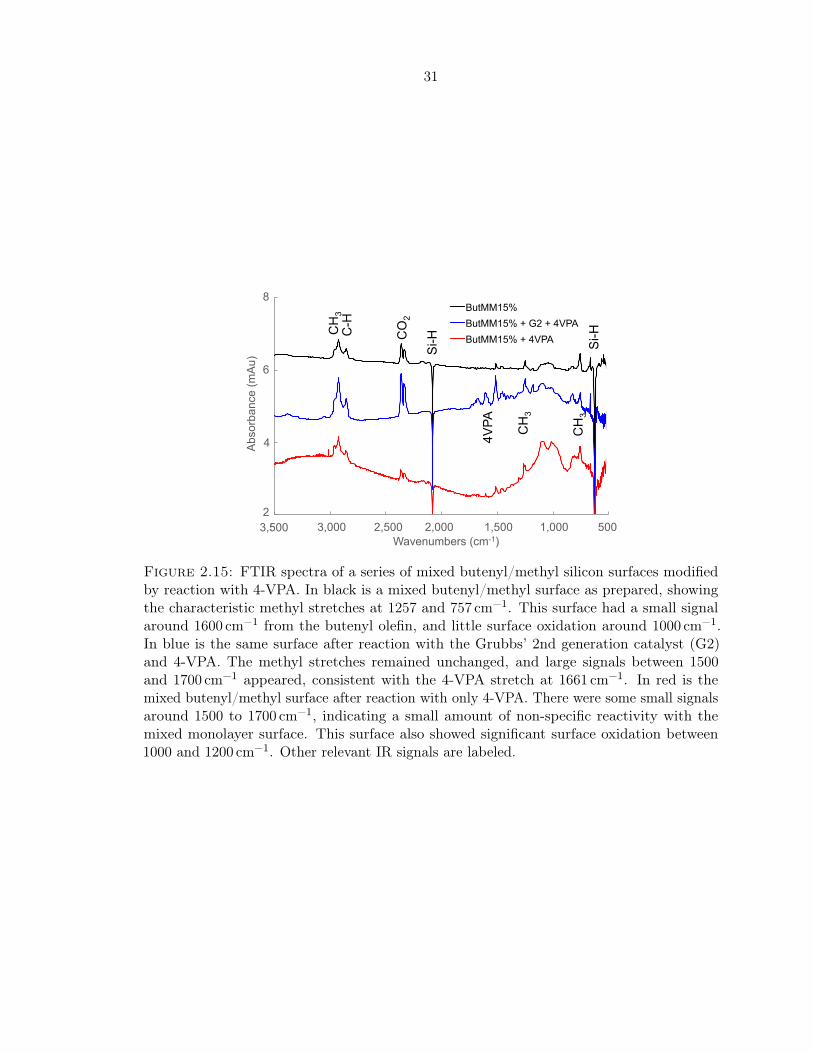
31
0.002
0.004
0.006
0.008
500 1,000 1,500 2,000 2,500 3,000 3,500
ButMM15% ButMM15% + G2 + 4VPA ButMM15% + 4VPA
2,500 1,500 500 Wavenumbers (cm-1)
3,000 2,000 1,000
8
Abs
orba
nce
(mA
u)
6
4
2 3,500
CO
2
Si-H
CH
3
CH
3
C-H
4VPA
CH
3 S
i-H
Figure 2.15: FTIR spectra of a series of mixed butenyl/methyl silicon surfaces modifiedby reaction with 4-VPA. In black is a mixed butenyl/methyl surface as prepared, showingthe characteristic methyl stretches at 1257 and 757 cm−1. This surface had a small signalaround 1600 cm−1 from the butenyl olefin, and little surface oxidation around 1000 cm−1.In blue is the same surface after reaction with the Grubbs’ 2nd generation catalyst (G2)and 4-VPA. The methyl stretches remained unchanged, and large signals between 1500and 1700 cm−1 appeared, consistent with the 4-VPA stretch at 1661 cm−1. In red is themixed butenyl/methyl surface after reaction with only 4-VPA. There were some small signalsaround 1500 to 1700 cm−1, indicating a small amount of non-specific reactivity with themixed monolayer surface. This surface also showed significant surface oxidation between1000 and 1200 cm−1. Other relevant IR signals are labeled.
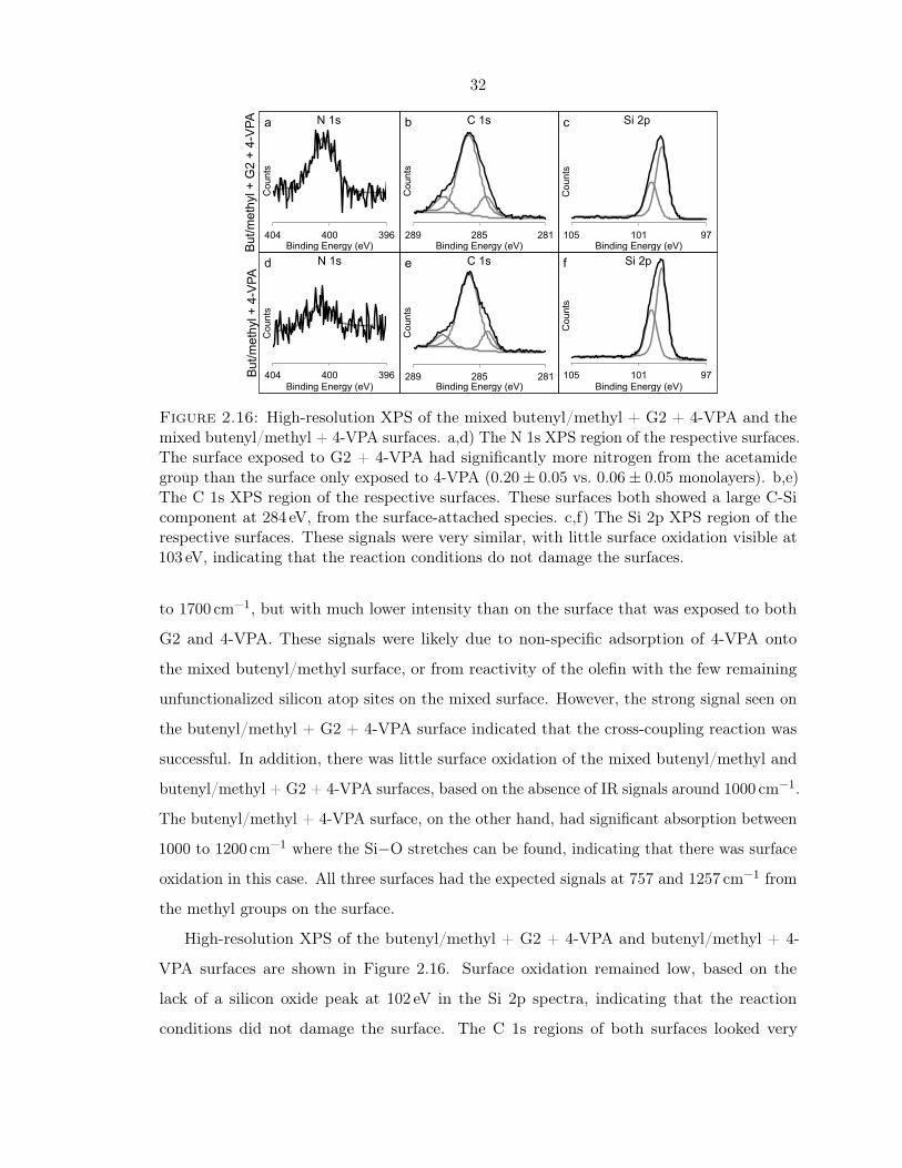
32
97 101 105
Cou
nts
Binding Energy (eV)
Si 2p
281 285 289
Cou
nts
Binding Energy (eV)
C 1s
396 400 404
Cou
nts
Binding Energy (eV)
N 1s
97 101 105
Cou
nts
Binding Energy (eV)
Si 2p
281 285 289
Cou
nts
Binding Energy (eV)
C 1s
396 400 404
Cou
nts
Binding Energy (eV)
N 1s
a b
d e
c
f B
ut/m
ethy
l + G
2 +
4-V
PA
But
/met
hyl +
4-V
PA
Figure 2.16: High-resolution XPS of the mixed butenyl/methyl + G2 + 4-VPA and themixed butenyl/methyl + 4-VPA surfaces. a,d) The N 1s XPS region of the respective surfaces.The surface exposed to G2 + 4-VPA had significantly more nitrogen from the acetamidegroup than the surface only exposed to 4-VPA (0.20± 0.05 vs. 0.06± 0.05 monolayers). b,e)The C 1s XPS region of the respective surfaces. These surfaces both showed a large C-Sicomponent at 284 eV, from the surface-attached species. c,f) The Si 2p XPS region of therespective surfaces. These signals were very similar, with little surface oxidation visible at103 eV, indicating that the reaction conditions do not damage the surfaces.
to 1700 cm−1, but with much lower intensity than on the surface that was exposed to both
G2 and 4-VPA. These signals were likely due to non-specific adsorption of 4-VPA onto
the mixed butenyl/methyl surface, or from reactivity of the olefin with the few remaining
unfunctionalized silicon atop sites on the mixed surface. However, the strong signal seen on
the butenyl/methyl + G2 + 4-VPA surface indicated that the cross-coupling reaction was
successful. In addition, there was little surface oxidation of the mixed butenyl/methyl and
butenyl/methyl + G2 + 4-VPA surfaces, based on the absence of IR signals around 1000 cm−1.
The butenyl/methyl + 4-VPA surface, on the other hand, had significant absorption between
1000 to 1200 cm−1 where the Si−O stretches can be found, indicating that there was surface
oxidation in this case. All three surfaces had the expected signals at 757 and 1257 cm−1 from
the methyl groups on the surface.
High-resolution XPS of the butenyl/methyl + G2 + 4-VPA and butenyl/methyl + 4-
VPA surfaces are shown in Figure 2.16. Surface oxidation remained low, based on the
lack of a silicon oxide peak at 102 eV in the Si 2p spectra, indicating that the reaction
conditions did not damage the surface. The C 1s regions of both surfaces looked very

33
similar, with a peak at 284 eV from the silicon-bound carbons. The butenyl/methyl + G2
+ 4-VPA surface had a N 1s peak at 401 eV corresponding to 0.20± 0.05 monolayers of
4-VPA on the surface. Details of surface coverage calculations using XPS can be found in
Appendix B.1.1. The butenyl/methyl + 4-VPA surface also had a small N 1s peak at 401 eV
corresponding to 0.06± 0.05 monolayers of 4-VPA on the surface. This number was almost
within experimental error, suggesting that nonspecific adsorption or reaction of the 4-VPA
with the mixed butenyl/methyl surface was limited. This was consistent with the FTIR data,
which showed a larger 4-VPA signal on the surface exposed to both G2 and 4-VPA than on
the surface exposed to 4-VPA only. This indicated that the cross-coupling reaction with
G2 was successful on the mixed butenyl/methyl surface under these conditions, with little
non-specific reaction of the 4-VPA with the surface.
2.4.2 4-VinylPhenyl Isocyanide
The attachment of 4-VPA to the surface via cross-coupling with G2 was apparently successful.
4-VPI, which can act as a ligand to the Codmg complex shown in Figure 2.13-4, is an analogue
of 4-VPA and should react with the mixed butenyl/methyl surface in a similar manner. This
molecule does not have an easily distinguished IR signal, but the nitrogen of the isocyanide
group can be used as an XPS tag to characterize the reaction product. Cross-coupling of
4-VPI to the surface was done similarly to the 4-VPA, in a two-step process starting from
the mixed butenyl/methyl surface. Experimental details for this reaction can be found in
Appendix A.6. High-resolution XPS of a mixed methyl/butenyl surface modified with 4-VPI
is shown in Figure 2.17a-c. The N 1s signal of the butenyl/methyl + G2 + 4-VPI surface had
a peak corresponding to 0.15± 0.05 monolayers, indicating that the cross-coupling reaction
was successful on this surface. The Si 2p region had no peak at 103 eV, indicating that the
surface was not oxidized during the functionalization and cross-coupling reactions. The C 1s
region retained the peak at 284 eV from the carbon directly bound to silicon from the methyl
and butenyl groups.
Metallation of the surface with the Codmg complex was performed by soaking the
butenyl/methyl + G2 + 4-VPI modified surface in a solution of 10mg Codmg in 8mL
CH3CN for 2.5 h at RT. The experimental details for metallation with Codmg can be found
in Appendix A.7. The XPS of the metallated surface is shown in Figure 2.17d-f. A F 1s
peak at 688 eV appeared from the BF2 groups in the Codmg complex, corresponding to

34
97 101 105
Cou
nts
Binding Energy (eV)
Si 2p
281 285 289 C
ount
s Binding Energy (eV)
C 1s
397 401 405
Cou
nts
Binding Energy (eV)
N 1s
397 401 405
Cou
nts
Binding Energy (eV)
N 1s
683 688 693
Cou
nts
Binding Energy (eV)
F 1s
773 787 801 C
ount
s Binding Energy (eV)
Co 2p
But
/met
hyl/4
-VP
I B
ut/m
etth
yl/4
-VP
I + C
odm
g
a b
d e
c
f
Figure 2.17: High-resolution XPS of mixed butenyl/methyl surfaces modified by cross-coupling with 4-VPI and metallated with Codmg. a, b, c) The N 1s, C 1s, and Si 2phigh-resolution XPS, respectively, of the mixed butenyl/methyl + G2 + 4-VPI surface. a)The N 1s peak at 400 eV from the isocyanide group indicated that the cross-coupling reactionwith 4-VPI was successful. This peak corresponded to 0.15± 0.05 monolayers of 4-VPI onthe surface. b) The C 1s peak had a large C−Si component at 284 eV, corresponding to0.75± 0.05 monolayers, indicative of high surface coverage. c) The Si 2p region showed littleoxidation of the silicon surface based on the absence of a Si−O peak at 103 eV. d, e, f) TheN 1s, F 1s, and Co 2p high-resolution XPS, respectively, of the butenyl/methyl + G2 +4-VPI surface after metallation with the Codmg complex. d) The N peak shifted to slightlyhigher energy, at 401 eV, consistent with ligation by Co. This peak also increased in intensity,to 0.20± 0.05 monolayers of nitrogen. e) The F 1s region had a peak at 688 eV from theBF2 groups of the Codmg complex. f) The Co 2p region had a doublet of peaks at 782 and797 eV from the Codmg complex, indicating that the complex is intact on the surface.
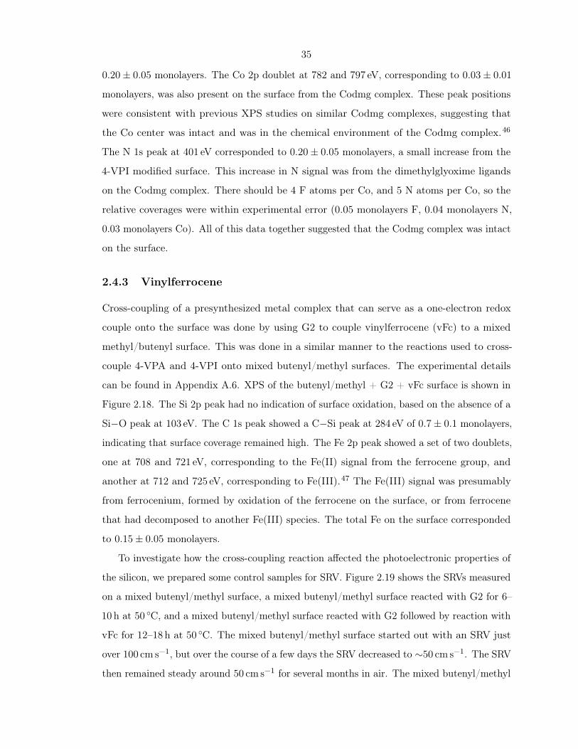
35
0.20± 0.05 monolayers. The Co 2p doublet at 782 and 797 eV, corresponding to 0.03± 0.01
monolayers, was also present on the surface from the Codmg complex. These peak positions
were consistent with previous XPS studies on similar Codmg complexes, suggesting that
the Co center was intact and was in the chemical environment of the Codmg complex.46
The N 1s peak at 401 eV corresponded to 0.20± 0.05 monolayers, a small increase from the
4-VPI modified surface. This increase in N signal was from the dimethylglyoxime ligands
on the Codmg complex. There should be 4 F atoms per Co, and 5 N atoms per Co, so the
relative coverages were within experimental error (0.05 monolayers F, 0.04 monolayers N,
0.03 monolayers Co). All of this data together suggested that the Codmg complex was intact
on the surface.
2.4.3 Vinylferrocene
Cross-coupling of a presynthesized metal complex that can serve as a one-electron redox
couple onto the surface was done by using G2 to couple vinylferrocene (vFc) to a mixed
methyl/butenyl surface. This was done in a similar manner to the reactions used to cross-
couple 4-VPA and 4-VPI onto mixed butenyl/methyl surfaces. The experimental details
can be found in Appendix A.6. XPS of the butenyl/methyl + G2 + vFc surface is shown in
Figure 2.18. The Si 2p peak had no indication of surface oxidation, based on the absence of a
Si−O peak at 103 eV. The C 1s peak showed a C−Si peak at 284 eV of 0.7± 0.1 monolayers,
indicating that surface coverage remained high. The Fe 2p peak showed a set of two doublets,
one at 708 and 721 eV, corresponding to the Fe(II) signal from the ferrocene group, and
another at 712 and 725 eV, corresponding to Fe(III).47 The Fe(III) signal was presumably
from ferrocenium, formed by oxidation of the ferrocene on the surface, or from ferrocene
that had decomposed to another Fe(III) species. The total Fe on the surface corresponded
to 0.15± 0.05 monolayers.
To investigate how the cross-coupling reaction affected the photoelectronic properties of
the silicon, we prepared some control samples for SRV. Figure 2.19 shows the SRVs measured
on a mixed butenyl/methyl surface, a mixed butenyl/methyl surface reacted with G2 for 6–
10 h at 50 C, and a mixed butenyl/methyl surface reacted with G2 followed by reaction with
vFc for 12–18 h at 50 C. The mixed butenyl/methyl surface started out with an SRV just
over 100 cm s−1, but over the course of a few days the SRV decreased to ∼50 cm s−1. The SRV
then remained steady around 50 cm s−1 for several months in air. The mixed butenyl/methyl
36
97 101 105
Cou
nts
Binding Energy (eV)
Si 2p
281 285 289
Cou
nts
Binding Energy (eV)
C 1s
702 712 722 732 C
ount
s Binding Energy (eV)
Fe 2p a b c
Figure 2.18: High-resolution XPS of the mixed butenyl/methyl surface with vinylferrocene(vFc) cross-coupled to the surface using the Grubbs’ 2nd generation catalyst. a) The Fe 2psignal, corresponding to 0.15± 0.05 monolayers, indicated that the cross-coupling reactionwas successful. b) The C 1s signal had a C−Si peak at 284 eV corresponding to 0.7± 0.1monolayers, indicating high surface coverage. c) The Si 2p peak showed little to no surfaceoxidation at 103 eV.
surface reacted with G2 had an SRV that remained steady at 40± 5 cm s−1 over the course
of several months. The mixed butenyl/methyl surface reacted with G2 followed by reaction
with vFc had an SRV of 55± 10 cm s−1 over several months. These surfaces all maintained
SRVs of around 50 cm s−1 for months while sitting in air. Silicon surfaces with SRVs of
<100 cm s−1 were generally considered to have reasonable photoelectronic properties. This
indicated that the photoelectronic properties of these surfaces were not adversely affected by
the cross-coupling reaction.
Electrochemistry on the mixed butenyl/methyl surfaces with cross-coupled vFc were
performed in an Ar-purged glove box. The experimental details of the electrochemistry setup
can be found in Appendix B.4. Figure 2.20 shows that there was a reversible electrochemical
signal at 0.1V vs. Ag/AgNO3 in CH3CN with 0.10M tetraethylammonium perchlorate
((NEt4)ClO4) as the supporting electrolyte from the surface-attached Fc/Fc+ couple. This
was consistent with previous studies on surface-attached ferrocene on silicon surfaces under
similar experimental conditions.48 Figure 2.20 shows the peak current density vs. the scan rate
and vs. the square root of the scan rate. The peak current had a linear dependence on scan
rate, indicating that the redox couple was surface-bound.49 The peak current was clearly non-
linear with the square root of the scan rate, which indicated that this was not a diffusional
process. Integration of the anodic and cathodic current vs. time gave the total charge
transferred to the redox couple, which was used as a measure of the electroactive material
on the surface. Details of this surface coverage calculation can be found in Appendix B.4.1.
The total coverage measured electrochemically was 0.03± 0.01 monolayers of ferrocene. This

37
0
50
100
0 10 20 30 40 50 60
SR
V (c
m s
-1)
Time (days)
Butenyl/methyl
Butenyl/methyl + G2
Butenyl/methyl + G2 + vFc
Figure 2.19: Surface recombination velocity (SRV) measured on a series of mixedbutenyl/methyl surfaces after cross-coupling reactions over 60 days in air. In blue (di-amonds), a mixed butenyl/methyl surface. In red (squares), a mixed butenyl/methyl surfacereacted with the Grubbs’ 2nd generation catalyst (G2). In green (triangles), a mixedbutenyl/methyl surface reacted with G2 followed by reaction with vinylferrocene (vFc). Allthree surfaces had SRVs of ∼50 cm s−1 over the course of several months, indicating thatthese surfaces had long charge-carrier lifetimes, and therefore excellent photoelectrochemicalproperties.
was significantly lower than the XPS measurement indicated, but it was possible that the
oxidized ferrocenium seen in the Fe 2p spectrum was not electroactive on this surface. In
that case, the surface coverage of Fe(II) seen by XPS was similar to the electroactive vFc
coverage measured here.
XPS of the surface collected after the electrochemical cycling is shown in Figure 2.21.
The Si 2p region had no Si−O peak at 103 eV. This indicated that the surface was stable
under electrochemical conditions and had not oxidized. The C 1s region had a C−Si peak
at 284 eV, indicating that there were still carbonaceous surface-attached species. The Fe
2p region showed increased Fe(III) and decreased Fe(II) components as compared with
the XPS collected prior to redox cycling. The total Fe coverage on the surface after the
electrochemistry was 0.10± 0.05 monolayers, which indicated that some of the Fe was lost
from the surface. However, the electrochemically active Fe(II) component from the ferrocene
was still present after the electrochemical cycling and cleaning procedure. There was also a
new N 1s peak at 400 eV following electrochemical cycling. This could be due to residual
solvent, CH3CN, remaining on the surface, or it could be from possible contamination by
the electrolyte, (NEt4)ClO4.

38
0 10 20−10
0
10
0 250 500−10
0
10
−0.3 0 0.3−10
0
10
20
Potential (vs Ag/AgNO3)
Cur
rent
Den
sity
(µA
cm-2
)
J (µ
A cm
-2)
J (µ
A cm
-2)
Scan Rate (mV s-1)
Scan Rate ( mV s-1)
υ
Figure 2.20: Cyclic voltammetry of a mixed butenyl/methyl monolayer on silicon withvinylferrocene cross-coupled on using the Grubbs’ 2nd generation catalyst. Left: Therewas a reversible redox couple at 0.1V vs. Ag/AgNO3. Increasing scan rate (v) from 10 to500mV s−1 is indicated by the black arrow. Top right: The peak current density (J) waslinear with the scan rate, as predicted for a surface-attached redox couple. Bottom right:The peak current density (J) was not linear with the square root of the scan rate, indicatingthat this was not a diffusional process.
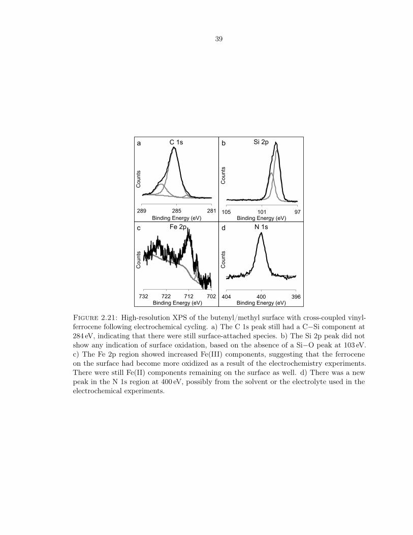
39
97 101 105
Cou
nts
Binding Energy (eV)
Si 2p
281 285 289
Cou
nts
Binding Energy (eV)
C 1s
396 400 404
Cou
nts
Binding Energy (eV)
N 1s
702 712 722 732
Cou
nts
Binding Energy (eV)
Fe 2p
a b
c d
Figure 2.21: High-resolution XPS of the butenyl/methyl surface with cross-coupled vinyl-ferrocene following electrochemical cycling. a) The C 1s peak still had a C−Si component at284 eV, indicating that there were still surface-attached species. b) The Si 2p peak did notshow any indication of surface oxidation, based on the absence of a Si−O peak at 103 eV.c) The Fe 2p region showed increased Fe(III) components, suggesting that the ferroceneon the surface had become more oxidized as a result of the electrochemistry experiments.There were still Fe(II) components remaining on the surface as well. d) There was a newpeak in the N 1s region at 400 eV, possibly from the solvent or the electrolyte used in theelectrochemical experiments.

40
2.5 Conclusion
These results showed that it was possible to cross-couple ferrocene to the mixed butenyl/methyl
surface using the Grubbs’ 2nd generation catalyst and form electrochemically active surfaces
with a surface-attached redox couple. We developed and characterized a new class of mixed
methyl/butenyl monolayers with controllable surface coverage of each species. We used the
Grubbs’ catalyst to form electroactive monolayers by cross-coupling vinylferrocene onto the
mixed methyl/butenyl surfaces. We showed that these mixed monolayers had excellent pho-
toelectronic properties, based on the low SRVs measured on mixed methyl/butenyl surfaces
before and after the cross-coupling reaction. This indicated that these electroactive surfaces
have the necessary properties for use in a solar-fuel forming device. However, many attempts
at this reaction with a variety of surfaces with varying amounts of butenyl never resulted in
greater than 0.05 monolayers of electrochemically active ferrocene on the surface. This could
be due to inherent steric constraints of the cross-coupling reaction, or it could be that the
reaction was simply inefficient. Our thorough investigations of this reaction have established
that this method of attachment for redox-active species resulted in low coverage, and was
therefore unlikely to be useful for photoelectrochemical devices.
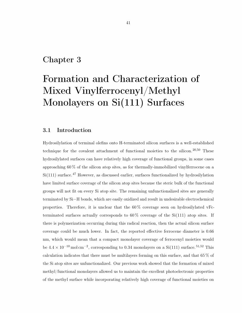
41
Chapter 3
Formation and Characterization ofMixed Vinylferrocenyl/MethylMonolayers on Si(111) Surfaces
3.1 Introduction
Hydrosilylation of terminal olefins onto H-terminated silicon surfaces is a well-established
technique for the covalent attachment of functional moieties to the silicon.20,50 These
hydrosilylated surfaces can have relatively high coverage of functional groups, in some cases
approaching 60% of the silicon atop sites, as for thermally-immobilized vinylferrocene on a
Si(111) surface.47 However, as discussed earlier, surfaces functionalized by hydrosilylation
have limited surface coverage of the silicon atop sites because the steric bulk of the functional
groups will not fit on every Si atop site. The remaining unfunctionalized sites are generally
terminated by Si−H bonds, which are easily oxidized and result in undesirable electrochemical
properties. Therefore, it is unclear that the 60% coverage seen on hydrosilylated vFc-
terminated surfaces actually corresponds to 60% coverage of the Si(111) atop sites. If
there is polymerization occurring during this radical reaction, then the actual silicon surface
coverage could be much lower. In fact, the reported effective ferrocene diameter is 0.66
nm, which would mean that a compact monolayer coverage of ferrocenyl moieties would
be 4.4× 10⁻¹⁰mol cm−2, corresponding to 0.34 monolayers on a Si(111) surface.51,52 This
calculation indicates that there must be multilayers forming on this surface, and that 65% of
the Si atop sites are unfunctionalized. Our previous work showed that the formation of mixed
methyl/functional monolayers allowed us to maintain the excellent photoelectronic properties
of the methyl surface while incorporating relatively high coverage of functional moieties on
42
5-60 min, 100oC
Fe
Fe
Cl
Si
Methyl GrignardTHF
60 min, 65oC
Cl
Si Si
H
Si
CH3
SiSi
PCl5, chlorobenzenebenzoyl peroxide
45-60 min, 90-100oC
Fe
Scheme 3.1: Reaction scheme for the formation of a mixed methyl/vFc monolayer onchlorinated Si(111) starting from a H-terminated Si(111) surface. Reprinted with permissionfrom Lattimer et al.34 Copyright 2013 American Chemical Society.
the surface as well. However, the steric requirements of the cross-coupling reactions described
in Chapter 2 limited the ultimate surface coverage of redox-active groups. Our aim in the
following chapter was to combine the high coverage of redox-active groups imparted by the
hydrosilylation reaction with the passivation and high surface coverage of methylation to
form a new class of mixed monolayers on silicon.
We describe herein the characterization of mixed monolayer surfaces that have been
prepared via radical reaction of an olefin with the Cl−Si(111) surface, followed by function-
alization of remaining reactive Si−Cl bonds with methyl groups via reaction with CH3MgCl
(Scheme 3.1). The approach is readily carried out with commercially available reagents
and avoids sterically demanding reagents or intermediates that could limit the coverage
of immobilized species. The method was demonstrated by incorporation of vinylferrocene
into a mixed vinylferrocenyl/methyl monolayer on Si(111) surfaces. Vinylferrocene has been
used frequently as a model redox couple for surface attachment due to the well-behaved
electrochemistry of vinylferrocene, as well as the ease of attaching vFc to silicon surfaces
via hydrosilylation.47,48,53 In this work, we show that the two-step halogenation/alkylation
method can be extended to allow the formation of a Si(111) surface that has electroactive
groups directly bound to the surface prior to the backfill of the remaining Cl−Si sites with
methyl groups, has a low interfacial charge-carrier recombination velocity, is protected against
oxidation, and displays photoelectrochemical activity that confirms facile charge transfer
from the silicon to the surface-attached redox species.
3.2 Methylation of H− and Cl−Si(111)
Methylation with a Grignard reagent requires a Cl−Si surface, while hydrosilylation requires
a H−Si surface. The obvious way to form a mixed monolayer using both these reactions

43
97 100 103 106
Cou
nts
Binding Energy (eV)
Si 2p Si-Cl + Me Si-H + Me
101 104
10x Mag
280 283 286 289
Cou
nts
(Offs
et)
Binding Energy (eV)
C 1s a b
Figure 3.1: Comparison of the high-resolution XPS data for the a) Si 2p and b) C 1s signalsof CH3−Si(111) surfaces produced by reaction of CH3MgCl with a Cl−Si(111) (blue, dashed)or H−Si(111) (black, solid) surface. The oxide peak at 102 eV in the Si 2p region is shownwith 10x magnification in the inset. The C 1s peak at 284 eV was ascribable to the carbonof the CH3 group that was directly bound to atop Si(111) sites. This peak on the surfaceformed on H−Si(111) had an area of ∼8% of the area of the peak for the CH3−Si(111)surfaces formed by reaction of CH3MgCl with Cl−Si(111). Adapted with permission fromLattimer et al.34 Copyright 2013 American Chemical Society.
would be to perform both of these reactions on the same starting surface. We used methyl
Grignard to functionalize both H- and Cl-terminated silicon to see if the reaction would be
equally successful on both starting surfaces. The results are shown in Figure 3.1.34 The
Si 2p region of both surfaces had little sign of surface oxidation, based on the very small
Si−O peak at 103 eV, corresponding to <0.1 monolayer of surface oxide. Details of the
surface coverage calculations using XPS can be found in Appendix B.1.1. The C 1s region
(Figure 3.1b) exhibited three peaks, with the lowest binding-energy component, at 284 eV,
corresponding to the carbon directly bound to silicon, and providing evidence that the surface
had been functionalized with Si−C bonds.13,29 The higher binding-energy signal, at 285 eV,
was ascribed to adventitious carbon bonded to carbon and/or hydrogen, and the 287 eV peak
was ascribed to adventitious carbon bonded to oxygen or other electronegative elements.13,29
In contrast, H−Si(111) surfaces that had been exposed to CH3MgCl, without formation of
the Cl−Si(111) intermediate surface, showed C 1s signals at 284 eV that had an area of ∼8%
of the corresponding peak on the CH3−Si(111) surfaces prepared by the two-step method
(Figure 3.1b). Hence H−Si(111) surfaces did not efficiently react with CH3MgCl, and so
the chlorination step was required under our reaction conditions to achieve a high yield of
surface functionalization.

44
97 101 105
Cou
nts
(nor
mal
ized
)
Binding Energy (eV)
Si 2p
101 103 105
10x mag
702 714 726
Cou
nts
(nor
mal
ized
, offs
et)
Binding Energy (eV)
Fe 2p Si-H + vFc 2h
Si-Cl + vFc 2h
282 285 288
Cou
nts
(nor
mal
ized
, offs
et)
Binding Energy (eV)
C 1s a b c
Figure 3.2: High-resolution XPS data of surfaces obtained by the thermal reaction of vFcwith H−Si(111) (black, solid) and Cl−Si(111) (blue, dashed) surfaces. The silicon oxidecomponent is shown expanded by 10x at 102–103 eV on both surfaces. The Fe 2p spectraexhibited large Fe(II) peaks at 708 and 721 eV that were ascribable to the presence of aferrocene moiety. The C 1s spectra of both surfaces had a single, broad peak at 285 eV.Reprinted with permission from Lattimer et al.34 Copyright 2013 American Chemical Society.
3.3 Thermal Reactions of H− and Cl−Si(111) with Vinylfer-
rocene
Figure 3.2 shows the high-resolution Si 2p, Fe 2p, and C 1s XPS data for H−Si(111) and
Cl−Si(111) surfaces that had been exposed to vFc for 3 h, followed by extensive rinsing
and sonication after synthesis and prior to characterization.34 Experimental details for the
preparation of these surfaces is found in Appendix A.8. The predominant state of iron on
both of these surfaces was Fe(II), with peaks arising from Fe(II)-derived ferrocene moieties
detected at 708 and 721 eV, with very minor Fe(III)-derived contributions at 712 and 725 eV
(Figure 3.2b).47 Less than 10% of a monolayer of Cl was detected on these surfaces. The C
1s region was best fit by a single peak at 285 eV (Figure 3.2c). No Fe was detected when
H−Si(111) or Cl−Si(111) surfaces were exposed to unsubstituted ferrocene under otherwise
the same reaction conditions.
The coverage of vinylferrocene-derived Fe on surfaces produced by the reaction of
H−Si(111) and Cl−Si(111) surfaces with vFc was calculated to be ηFe = 0.8 ± 0.1 and
ηFe = 1.1 ± 0.1 monolayers, or Fe atoms per Si atop site, respectively. Details of the surface
coverage quantification using XPS can be found in Appendix B.4.1. Because the subtended
area of a vFc molecule is much larger than the area of a Si atom on an unreconstructed
Si(111) surface, the measured Fe coverage indicates that multiple layers of vFc were attached
to the surface.51 Both surfaces contained submonolayer levels of oxidized Si, as evidenced by

45
a broad signal at 102 eV,40 whose area corresponded to 0.3± 0.1 and 0.4± 0.1 monolayers for
Cl−Si(111) and H−Si(111) surfaces, respectively, that had been exposed to vFc (Figure 3.2a).
A large C 1s signal at 285 eV was observed for the vFc-exposed surfaces (Figure 3.2c), and
this peak is attributable to a combination of the 12 carbon atoms from the ferrocene moiety,
as well as to adventitious carbon on the functionalized surface. We did not see a distinct
shoulder at 284 eV from surface-attached carbon, but the large peak at 285 eV may have
obscured a small signal.
3.3.1 Electrochemistry of vFc-Terminated Si(111) Surfaces
The cyclic voltammetry of H−Si(111) and Cl−Si(111) surfaces that had been treated with
vFc exhibited a reversible redox couple at +0.1V versus Ag/AgNO3 (Figure 3.3a,c). Under
virtually identical electrochemical conditions, the Fc/Fc+ couple has been observed at +0.08V
versus Ag/AgNO3 for vFc immobilized on Si(100) surfaces.48 The anodic and cathodic peak
current densities showed a linear dependence on the scan rate, indicating a surface-attached
redox reaction (Figure 3.3b,d).49 The total charge transferred was used to calculate the
number of electroactive Fc groups on the surface, which corresponded to ηFc = 0.9 ± 0.1 and
ηFc = 1.1 ± 0.1 Fc groups per Si atop site for H−Si(111) and Cl−Si(111) surfaces modified
with vFc, respectively. The details of this surface coverage calculation can be found in
Appendix B.4.1.
The separation of the anodic and cathodic peaks should be small, ideally equaling zero,
for a surface-bound redox couple, but will increase with scan rate if the rate of interfacial
charge-transfer is comparable to the voltammetric time scale.54 At a scan rate of 200mV s−1,
the anodic and cathodic peak separation was 50 and 46mV for H−Si(111) and Cl−Si(111)
surfaces, respectively. As a control, methyl-terminated p+-Si(111) electrodes were prepared
and used to investigate the electrochemistry of Fc in solution. These electrodes showed a
peak current density that depended on the square root of the scan rate, as expected for
freely diffusing redox couples in solution.49 The peak-to-peak separation was several hundred
mV at a scan rate of 100mV s−1, and increased with scan rate. Hence, the semiconductor
electrode contributed to the observed peak splitting for the ferrocene redox couple, precluding
a rigorous analysis by conventional methods used for metal electrodes. Nonetheless, the small
peak splitting observed on the vFc-modified H−Si(111) and Cl−Si(111) surfaces implied
relatively rapid charge transfer on the surface on this voltammetric time scale (∼50mV at

46
0 0.2 0.4−0.8
−0.4
0
0.4
0.8
0 0.5 1.0−0.6
−0.3
0
3
0.6
−0.2 0 0.2 0.4−2
−1
0
1
2
0 0.5 1.0−1
−0.5
0
0.5
1
Cur
rent
Den
sity
(mA
cm-2
) C
urre
nt D
ensi
ty (m
A cm
-2)
Cur
rent
Den
sity
(mA
cm-2
) C
urre
nt D
ensi
ty (m
A cm
-2)
Potential (vs. Ag/AgNO3)
Potential (vs. Ag/AgNO3)
Scan Rate (V s-1)
Scan Rate (V s-1)
a b
c d
υ
υ
Figure 3.3: Dark cyclic voltammetry of electrodes formed from reaction of p+-typeH−Si(111) or Cl−Si(111) reacted with vFc for 2 h at 140 C. a) Cyclic voltammetry of theH−Si(111) surface obtained at scan rates of 200 to 2000mV s−1, with increasing scan rate (v)indicated by the arrow. c) Cyclic voltammetry of the Cl−Si(111) surface obtained at scanrates of 150 to 3000mV s−1, with increasing scan rate indicated by the arrow. b,d) The linearrelationship between maximum current density and scan rate on the H−Si(111) surface (b)and Cl−Si(111) surface (d) is consistent with the presence of a surface-bound redox couple.Adapted with permission from Lattimer et al.34 Copyright 2013 American Chemical Society.
100mV s−1).
The similarity between these resultant surfaces indicated that the reaction between the
vFc and both the H- and Cl-terminated silicon surfaces was efficient and likely occurred via
similar mechanisms. The similarity of these surfaces suggested the presence of a mutually
similar link between the Fc group and both of these surfaces. The high surface coverage
of Fc on these surfaces suggested that the vFc polymerized on the surface. Polymerization
of similar aryl-olefins has been seen in other work on attaching groups to surfaces using
surface-initiated radical polymerization.55,56 The presence of multilayers made it difficult to
ascertain the exact termination of the silicon on these surfaces. We did not observe a C−Si
peak at 284 eV on these surfaces, and there was not significant surface oxidation. This left the
surface structure largely unknown, but the electrochemistry indicated that the vFc is attached

47
97 100 103 106
Cou
nts
Binding Energy (eV)
Si 2p
101 105
10x mag
266 270 274
Cou
nts
Binding Energy (eV)
Cl 2s
700 708 716 724
Cou
nts
Binding Energy (eV)
Fe 2p
280 283 286 289
Cou
nts
Binding Energy (eV)
C 1s
- Partial vFc - Mixed vFc/methyl
a
c
b
d
Figure 3.4: XPS data for partial vFc− (black) and mixed methyl/vFc− (blue) modifiedSi(111) surfaces. a) High-resolution Si 2p region. A Si−O peak at 103 eV was observed forthe partial vFc−Si(111) surface but was not observed on the mixed methyl/vFc−Si(111)surface. b) High-resolution C 1s region. The mixed methyl/vFc−Si(111) surface had a peakat 284 eV ascribable to the Si-bound CH3 group, shown in light blue, that was not resolvedin the spectrum of the partial vFc−Si(111) surface. c) High-resolution Cl 2s region. Morechlorine was observed on the partial vFc−Si(111)surface, as evidenced by the Cl 2s peakat 270 eV, than on the mixed methyl/vFc−Si(111)surface. d) High-resolution Fe 2p region,showing similar coverages of Fe on these two surfaces. Reprinted with permission fromLattimer et al.34 Copyright 2013 American Chemical Society.
to the surface through a stable linker. This was supported by studies using unsubstituted
ferrocene, which did not result in any surface attachment of the ferrocene moiety by XPS,
suggesting that the vinyl group was necessary for surface attachment. Surfaces terminated
by methyl groups prior to reaction with vFc showed no Fe signal by XPS, indicating that the
reaction between the vFc and the Cl-terminated surface occurred through the Cl−Si bond
and not by non-specific adsorption of the vFc group to the silicon. While these results were
promising regarding the ability to use the Cl-terminated silicon surface as a starting point
for the formation of mixed monolayers, we would have preferred a more controlled process
for surface attachment that did not result in multilayers and poorly characterized surface
species.
48
3.3.2 Mixed Methyl/Vinylferrocenyl Surfaces
Scheme 3.1 shows the reaction sequence for the formation of mixed methyl/vinylferrocenyl
surfaces. These surfaces were chlorinated, and the Cl−Si(111) surface was then first reacted
with vFc for a predetermined time period, followed by reaction with methyl Grignard.
Figure 3.4 presents the high-resolution XPS data for a Cl−Si(111) surface that was reacted
thermally with vFc for 30min (partial vFc) as well as for a Cl−Si(111) surface that was reacted
thermally with vFc for 20min and then methylated using CH3MgCl (mixed methyl/vFc).
Fe(II) peaks at 708 and 721 eV were observed in the Fe 2p region in both cases, with Fe
coverages of ηFe = 0.15 ± 0.05 and ηFe = 0.10 ± 0.05 monolayers for the partial vFc- and
mixed methyl/vFc-terminated surfaces, respectively (Figure 3.4d). The lower coverage of Fe
on these vFc-functionalized surfaces as compared to the vFc−Si(111) surfaces depicted in
Figure 3.2 was consistent with only partial functionalization of the Si surface occurring with
shorter reaction times (30min vs. 3 h). The surface oxide coverage, measured from the Si−O
peak at 102 eV from the Si 2p XPS signal, was ηSi−O = 0.8 ± 0.1 monolayers on the partially
vFc-terminated Si surface but was below the detection limit (<0.01 monolayer) on the mixed
methyl/vFc surface (Figure 3.4a). The C 1s signal on the partial vFc-terminated Si(111)
surface was a broad peak centered at 285 eV with a total area that corresponded to 4.0± 0.5
C per Si atop site. This would correspond to around 0.3 monolayers of ferrocene, which
indicated that there was some adventitious carbon contribution on this surface. The mixed
methyl/vFc−Si(111) surface C 1s signal also exhibited a large peak at 285 eV, corresponding
to 3.0± 0.5 monolayers of C, with a shoulder at 284 eV that yielded upon curve-fitting
analysis a best fit to 0.5± 0.1 monolayers of Si−CH3 per Si atop site (Figure 3.4b). The
peak at 284 eV indicates that there are methyl groups on the surface in addition to the
vFc groups seen by the Fe 2p signal.13,29 This indicates that we have successfully formed a
mixed methyl/vFc monolayer on the surface. Based on the Cl 2s XPS signal at 270 eV, the
partial vFc surface exhibited a Cl coverage of 0.5± 0.1 monolayers, compared to 0.1± 0.1
monolayers of Cl on the mixed methyl/vFc surface (Figure 3.4c). This was consistent with our
reaction scheme wherein the remaining chlorine groups on the surface after partial reaction
with vFc are available to react with methyl Grignard to form the mixed monolayer.

49
−0.2 0 0.2 0.4
−1
−0.5
0
0.5
1
−0.2 0 0.2
−0.4
0
0.4
0 25 50−1.0
−0.5
0
0.5
1.0
0 25 50−2
0
2
Cur
rent
Den
sity
(mA
cm-2
) C
urre
nt D
ensi
ty (m
A cm
-2)
Cur
rent
Den
sity
(mA
cm-2
) C
urre
nt D
ensi
ty (m
A cm
-2)
Potential (vs. Ag/AgNO3)
Potential (vs. Ag/AgNO3)
Scan Rate (V s-1)
Scan Rate (V s-1)
a b
c d
υ
υ
Figure 3.5: Cyclic voltammetry of partial vFc-terminated and mixed methyl/vFc-terminatedp+ Si(111) surfaces. a) Cyclic voltammetry of the partial vFc-terminated Si(111) surfaceat scan rates of 0.05 to 25V s−1, with increasing scan rate (v) indicated by the arrow. c)Cyclic voltammetry of the mixed methyl/vFc surface at scan rates of 0.05 to 25V s−1, withincreasing scan rate indicated by the arrow. b,d) The linear relationship between maximumcurrent density and scan rate on the partial vFc−Si(111) (b) and mixed methyl/vFc−Si(111)(d) electrodes is consistent with the presence of a surface-bound redox couple. Adapted withpermission from Lattimer et al.34 Copyright 2013 American Chemical Society.
50
3.3.3 Electrochemistry of Mixed Methyl/Vinylferrocenyl Surfaces
Figure 3.5 shows the cyclic voltammetric data for the partial vFc-functionalized and mixed
methyl/vFc-functionalized Si(111) surfaces. Both surfaces had a reversible redox couple
at +0.10V vs. Ag/AgNO3, with a linear dependence of the peak current density on the
scan rate, as expected for a surface-attached redox couple.49 After background subtraction,
integration of the anodic and cathodic current versus time was analyzed to obtain the total
charge transferred, giving an electrochemically active surface coverage of vFc, ηFc. The
details of this calculation can be found in Appendix B.4.1. The average surface coverage
of vFc on the partial vFc and mixed methyl/vFc surfaces at a variety of scan rates was
ηFc = 0.08± 0.03 and 0.03± 0.01 monolayers, respectively. The surface coverage did not
vary with the scan rate or the scan number, but remained steady throughout the course
of the electrochemical cycling, within experimental error, for both surfaces. This indicates
that the surface functionalization was stable to the electrochemical conditions, and there
was no loss of electroactive ferrocene from the surface due to the electrochemical cycling.
The peak-to-peak splitting at 200mV s−1 was 57mV for the partial vFc-terminated Si(111)
surface and 39mV for the mixed methyl/vFc-terminated Si(111) surface, indicating rapid
interfacial charge transfer on this time scale (200mV s−1).
Figure 3.6 shows the coverage of vFc incorporated into mixed methyl/vFc monolayers
as a function of the reaction time between vFc and the Cl−Si(111) surfaces, as measured
electrochemically by determination of ηFc. The coverage of electroactive vFc groups incorpo-
rated into the mixed monolayers increased from 0.01 to 0.3 monolayers with the duration of
the exposure to vFc from 10 to 60min, and could be reproducibly controlled by variation in
the duration of the exposure.
Figure 3.7a shows the Si 2p region of the partial vFc-terminated and mixed methyl/vFc-
terminated Si(111) surfaces after >30 redox cycles had been performed on the electrode
surfaces. The partial vFc-terminated Si(111) surface showed a large Si−O peak at 103 eV,
corresponding to 2.8± 0.5 monolayers of silicon oxide, which indicated that the surface had
been extensively oxidized during electrochemical cycling (cf Figure 3.3a). In contrast, the
mixed methyl/vFc-terminated Si(111) surface showed 0.4± 0.1 monolayers of surface oxide
after redox cycling. The Fe 2p regions of both surfaces were largely unchanged from the
spectra obtained before redox cycling (Figure 3.7b and Figure 3.4d). After electrochemistry,
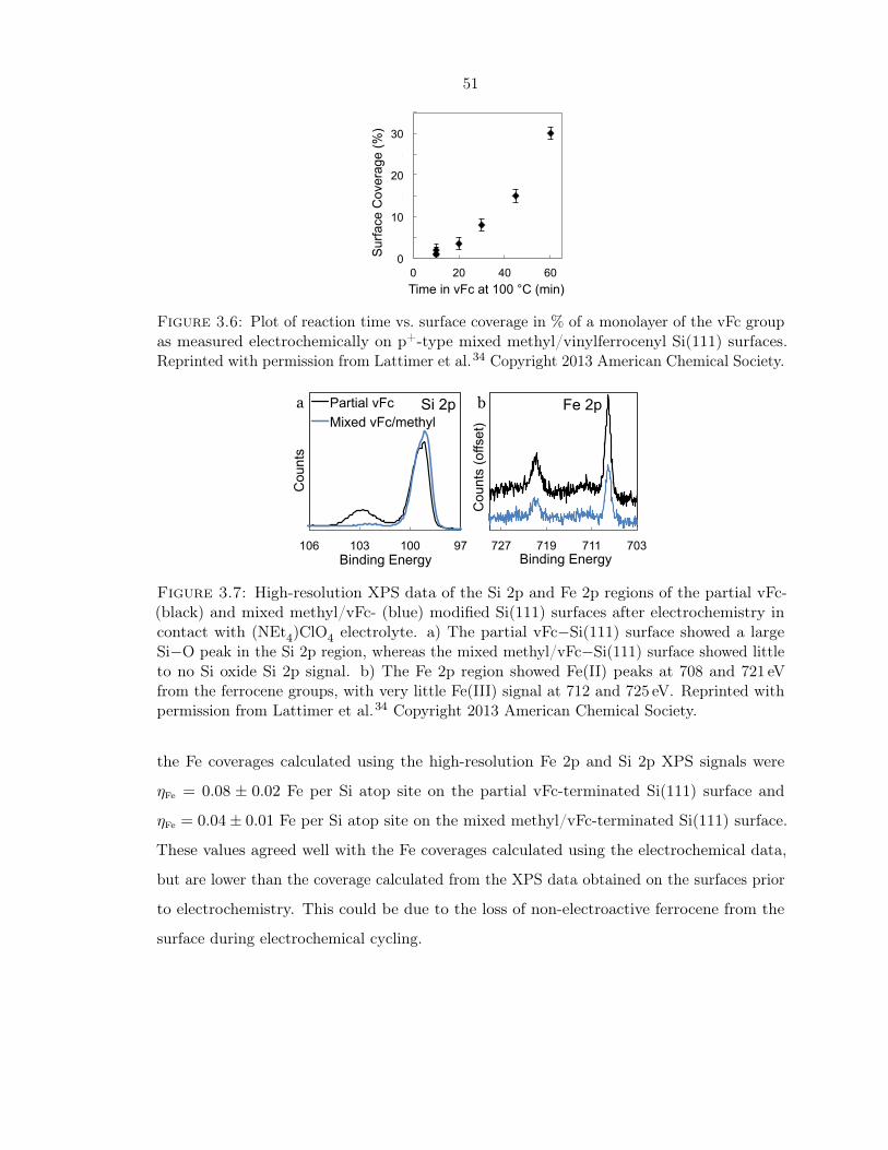
51
0
5
10
15
20
25
30
35
0 20 40 60
Sur
face
Cov
erag
e (%
)
Time in vFc 100 C (min) Time in vFc at 100 °C (min)
Figure 3.6: Plot of reaction time vs. surface coverage in % of a monolayer of the vFc groupas measured electrochemically on p+-type mixed methyl/vinylferrocenyl Si(111) surfaces.Reprinted with permission from Lattimer et al.34 Copyright 2013 American Chemical Society.
703 711 719 727
Cou
nts
(offs
et)
Binding Energy
Fe 2p
97 100 103 106
Cou
nts
Binding Energy
Si 2p Partial vFc Mixed vFc/methyl
b a
Figure 3.7: High-resolution XPS data of the Si 2p and Fe 2p regions of the partial vFc-(black) and mixed methyl/vFc- (blue) modified Si(111) surfaces after electrochemistry incontact with (NEt4)ClO4 electrolyte. a) The partial vFc−Si(111) surface showed a largeSi−O peak in the Si 2p region, whereas the mixed methyl/vFc−Si(111) surface showed littleto no Si oxide Si 2p signal. b) The Fe 2p region showed Fe(II) peaks at 708 and 721 eVfrom the ferrocene groups, with very little Fe(III) signal at 712 and 725 eV. Reprinted withpermission from Lattimer et al.34 Copyright 2013 American Chemical Society.
the Fe coverages calculated using the high-resolution Fe 2p and Si 2p XPS signals were
ηFe = 0.08 ± 0.02 Fe per Si atop site on the partial vFc-terminated Si(111) surface and
ηFe = 0.04 ± 0.01 Fe per Si atop site on the mixed methyl/vFc-terminated Si(111) surface.
These values agreed well with the Fe coverages calculated using the electrochemical data,
but are lower than the coverage calculated from the XPS data obtained on the surfaces prior
to electrochemistry. This could be due to the loss of non-electroactive ferrocene from the
surface during electrochemical cycling.
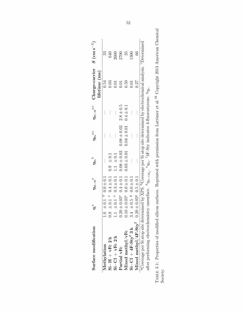
52
Surfacemod
ification
ηia
ηSi−
Oa
ηFcb
ηFea,c
ηSi−
Oa,c
Charge-carrier
S(cms−
1)
lifetime(m
s)Methy
lation
1.0
±0.1
d0.0±
0.1
——
—0.54
33Si−H
+vF
c2h
0.9
±0.1
e0.4±
0.1
0.9
±0.1
——
0.03
640
Si−Cl+
vFc2h
1.1
±0.1
e0.3±
0.1
1.1
±0.1
——
0.01
2600
Partial
vFc
0.20
±0.05
e0.4±
0.1
0.08
±0.03
0.08
±0.02
2.8±
0.5
0.01
2700
Mixed
methy
l/vF
c0.10
±0.05
e0.0±
0.1
0.03
±0.01
0.04
±0.01
0.4±
0.1
0.50
35Si−Cl+
4F-Sty
f3h
3.4
±0.5
g0.0±
0.1
——
—0.01
1300
Mixed
methy
l/4F
-Sty
f0.20
±0.05
g0.5±
0.1
——
—0.27
66a C
overag
epe
rSia
topsite
determ
ined
byXPS.
bCoverag
epe
rSia
topsite
determ
ined
byelectrochemical
analysis.c D
etermined
afterpe
rformingelectroche
mistryon
surface.
dη S
i−C
H3.e η
Fe.
f 4F-Sty
indicates4-flu
orostyrene
.g η
F.
Tabl
e3.
1:Prope
rtiesof
mod
ified
silicon
surfaces.Reprinted
withpe
rmission
from
Lattim
eret
al.34Cop
yright
2013
American
Chemical
Society.

53
3.3.4 Charge-Carrier Lifetimes of Mixed Methyl/Vinylferrocenyl Mono-
layers
Table 3.1 presents the observed charge-carrier lifetimes and inferred S values for the surfaces
described in this section. Details of the experimental set-up and S value calculations can
be found in Appendix B.3. H−Si(111) and Cl−Si(111) surfaces modified by vFc exhibited
photogenerated charge-carrier lifetimes of 27± 5ms and 7± 5ms, respectively, corresponding
to S = 640 ± 20 and S = 2600 ± 100 cm s−1, respectively. For comparison, CH3−Si(111)
surfaces had charge-carrier lifetimes of 550± 50ms, corresponding to S = 30±5 cm s−1. The
partial vFc-terminated and mixed methyl/vFc-terminated Si(111) surfaces exhibited charge-
carrier lifetimes of 10± 5 and 500± 50µs, respectively, corresponding to S = 2700± 100 and
S = 35 ± 5 cm s−1, respectively. The 4-fluorostyrene-functionalized Si(111) surface exhibited
a charge-carrier lifetime of 14± 5 µs, which corresponded to S = 1300 ± 100 cm s−1, whereas
the mixed methyl/4-fluorostyrene-terminated Si(111) surface had a charge-carrier lifetime
of 270± 50 µs, corresponding to S = 66 ± 5 cm s−1, which was similar to the value of S
measured on the mixed methyl/vFc-terminated Si(111) surface. Experimental details for the
formation of the 4-fluorostyrene modified surfaces can be found in Appendix A.9.
The low SRVs measured on the mixed methyl/vFc and mixed methyl/4-fluorostyrene
surfaces were comparable to the SRV of the methyl-terminated surface. This indicated that
these surfaces had good photoelectronic properties and did not facilitate fast charge-carrier
recombination at the surface. However, if holes were to transfer to the attached Fc upon
illumination of intrinsic silicon, the reduced concentration of holes on the surface could result
in extended charge-carrier lifetimes. 4-Fluorostyrene, which is chemically similar to the
vinyl-appended cyclopentadienyl (Cp) ring in vFc, is not redox active and cannot act as
a Faradaic hole acceptor. Mixed 4-fluorostyrene/methyl Si(111) surfaces also showed the
relatively long charge-carrier lifetimes and low S values characteristic of a well-passivated
and stable Si surface. Thus the low S values of the mixed methyl/vFc-terminated Si(111)
surfaces can be attributed to low rates of charge-carrier recombination on a well-passivated
surface, rather than the redox properties of the Fc molecule on the surface. These long
charge-carrier lifetimes should therefore make these electrons and holes available for chemical
reactions on these surfaces under photoelectrochemical conditions.

54
3.3.5 Photoelectrochemistry of Mixed Methyl/Vinylferrocenyl Surfaces
on n-type Si
Figure 3.8 shows cyclic voltammetric data in the dark and under illumination of a mixed
methyl/vinylferrocenyl n-type Si electrode in CH3CN. Details of the photoelectrochemical
experiment can be found in Appendix B.4. In the dark, the ferrocene redox couple was
observed at ∼0.1V vs. Ag/AgNO3, similar to mixed methyl/vinylferrocenyl surfaces on
p+-type silicon (Figure 3.5). The potential of the ferrocene redox couple was taken as the
average of the potentials of the anodic and cathodic peak currents. On n-type silicon at a
scan rate of 1V s−1 the peak separation was ∼400mV in the dark, due to slow charge-transfer
kinetics (Figure 3.8). When the sample was illuminated by visible light, the ferrocene
redox couple became more reversible and the redox peak shifted to −0.3V vs. Ag/AgNO3,
indicating a photovoltage generated by the Si(111) of ∼0.4V. The peak-to-peak separation
under illumination was 10mV at 1V s−1, indicating facile charge transfer to the surface-
attached ferrocene. The average photovoltage generated on this surface at a variety of
scan rates was 360± 50mV, as determined by the difference between the redox potential
of the Fc couple on illuminated n-type Si and the redox potential observed on p+-type Si
in the dark (0.10V vs. Ag/AgNO3 on all the samples studied herein).57 This comparison
is illustrated in Figure 3.9, which shows representative cyclic voltammetric scans of mixed
methyl/vinylferrocenyl surfaces on p+-type Si in the dark and n-type Si under illumination,
at 10V s−1. The photovoltage decreased by ∼20% over several hours of scanning, although
the coverage of electrochemically active ferrocene groups remained stable.
We have developed a new method for forming mixed methyl/vinylferrocene monolayers
on Si(111) surfaces with relative ease and with a potentially large substrate scope. As an
example reaction system, vinylferrocene was attached at up to a ratio of 30% of the Si(111)
atop sites. The functionalized surfaces were resistant to oxidation and permitted relatively
rapid interfacial charge transfer to the attached ferrocene group. The mixed monolayers
maintained the favorable electronic properties of the underlying silicon, as evidenced by
the low surface recombination velocities measured on the functionalized surfaces, as well
as the 0.4 V photovoltage generated on n-type silicon. However, this method required a
relatively large amount (grams) of a thermally-stable, olefin-appended liquid substrate for
functionalization of the silicon. While vinylferrocene was an excellent test substrate that

55
Cur
rent
Den
sity
(µA
cm-2
)
Potential (vs. Ag/AgNO3)
Figure 3.8: Cyclic voltammetry (scan rate of 1V s−1) of a mixed methyl/vinylferrocenyln-type Si(111) electrode under illumination (blue) and in the dark (black). The photovoltagewas 0.4V, as determined by the shift in the average of the anodic and cathodic peak positionson illuminated n-Si relative to the position on p+-Si in the absence of illumination. Reprintedwith permission from Lattimer et al.34 Copyright 2013 American Chemical Society.
−1 −0.5 0 0.5−0.2
−0.1
0
0.1
0.2
LightDark
Cur
rent
Den
sity
(mA
cm-2
)
Potential (vs. Ag/AgNO3)
Figure 3.9: Cyclic voltammetry (scan rate of 10V s−1) of mixed methyl/vinylferrocenylelectrode surfaces on n-type Si(111) under illumination (blue) and on p+-type Si(111) inthe dark (black). The photovoltage observed was 0.44V. Reprinted with permission fromLattimer et al.34 Copyright 2013 American Chemical Society.
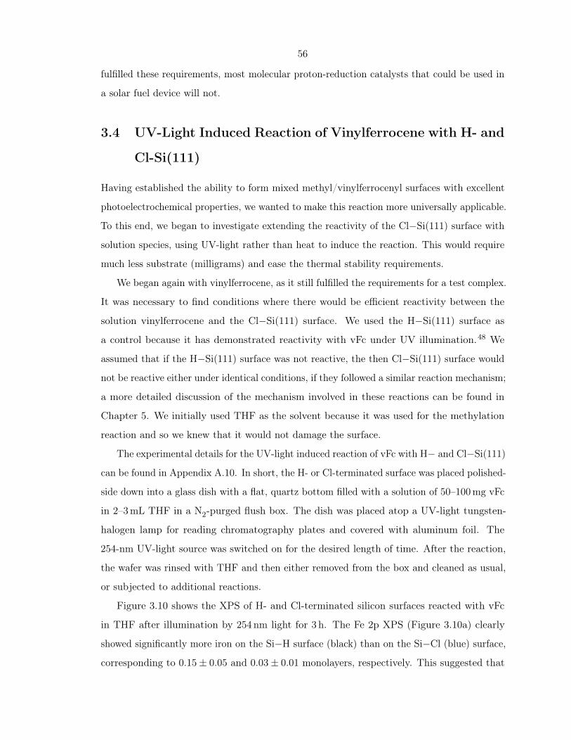
56
fulfilled these requirements, most molecular proton-reduction catalysts that could be used in
a solar fuel device will not.
3.4 UV-Light Induced Reaction of Vinylferrocene with H- and
Cl-Si(111)
Having established the ability to form mixed methyl/vinylferrocenyl surfaces with excellent
photoelectrochemical properties, we wanted to make this reaction more universally applicable.
To this end, we began to investigate extending the reactivity of the Cl−Si(111) surface with
solution species, using UV-light rather than heat to induce the reaction. This would require
much less substrate (milligrams) and ease the thermal stability requirements.
We began again with vinylferrocene, as it still fulfilled the requirements for a test complex.
It was necessary to find conditions where there would be efficient reactivity between the
solution vinylferrocene and the Cl−Si(111) surface. We used the H−Si(111) surface as
a control because it has demonstrated reactivity with vFc under UV illumination.48 We
assumed that if the H−Si(111) surface was not reactive, the then Cl−Si(111) surface would
not be reactive either under identical conditions, if they followed a similar reaction mechanism;
a more detailed discussion of the mechanism involved in these reactions can be found in
Chapter 5. We initially used THF as the solvent because it was used for the methylation
reaction and so we knew that it would not damage the surface.
The experimental details for the UV-light induced reaction of vFc with H− and Cl−Si(111)
can be found in Appendix A.10. In short, the H- or Cl-terminated surface was placed polished-
side down into a glass dish with a flat, quartz bottom filled with a solution of 50–100mg vFc
in 2–3mL THF in a N2-purged flush box. The dish was placed atop a UV-light tungsten-
halogen lamp for reading chromatography plates and covered with aluminum foil. The
254-nm UV-light source was switched on for the desired length of time. After the reaction,
the wafer was rinsed with THF and then either removed from the box and cleaned as usual,
or subjected to additional reactions.
Figure 3.10 shows the XPS of H- and Cl-terminated silicon surfaces reacted with vFc
in THF after illumination by 254 nm light for 3 h. The Fe 2p XPS (Figure 3.10a) clearly
showed significantly more iron on the Si−H surface (black) than on the Si−Cl (blue) surface,
corresponding to 0.15± 0.05 and 0.03± 0.01 monolayers, respectively. This suggested that

57
Si 2p C 1s Fe 2p a b c
280 285 290
Cou
nts
Binding Energy (eV) 96 101 106
Cou
nts
Binding Energy (eV) 700 715 730
Cou
nts
Binding Energy (eV)
Si-H Si-Cl Si-Cl+Methyl
Figure 3.10: XPS of Si−H and Si−Cl surfaces modified by reaction with vinylferrocene inTHF under illumination by UV light for 3 h. a) The high-resolution Fe 2p XPS of the Si−Hsurface after reaction with vFc (black), the Si−Cl surface after reaction with vFc (blue), andthe Si−Cl surface after reaction with vFc and methyl Grignard (red). There was significantlymore iron on the Si−H surface than the two Si−Cl surfaces, indicating that the Si−H surfacewas more reactive under these conditions. b) The high-resolution Si 2p XPS of the Si−Hsurface, in black, the Si−Cl surface, in blue, and the Si−Cl surface with addition reactionwith methyl Grignard, in red. The Si−Cl surface was extensively oxidized, as shown by thepeak at 103 eV, likely due to the lack of surface coverage by the vFc group leaving manyunfunctionalized Si atop sites. The lack of surface oxidation on the Si−Cl surface reactedwith both vFc and methyl Grignard indicated that the surface coverage on this surface washigher. c) The high-resolution C 1s XPS of the Si−H surface, in black, the Si−Cl surface,in blue, and the Si−Cl surface with additional reaction with methyl Grignard, in red. Theshoulder at 284 eV, which was only present on the Si−Cl surface reacted with both vFc andmethyl Grignard, indicated that a mixed methyl/vFc surface had been formed.
58
under the same conditions, the Si−H surface was more reactive than the Si−Cl surface.
This was not unexpected, based on the relatively long history of work on Si−H surface
functionalization.8 However, the attachment of any vFc to the Si−Cl surface allowed us to
use this reaction for mixed monolayer formation with methyl Grignard, which cannot be
done using the Si−H surface. This is shown in Figure 3.10, in red. The mixed monolayer
was formed by reacting the Si−Cl surface first with vFc for 3 h under UV illumination, and
then with methyl Grignard for 2 h. The Fe 2p XPS showed even less iron on this surface
than for the Cl−Si surface reacted with vFc without subsequent methylation, but there was
still some reactivity with vFc. The amount of Fe on this surface corresponded to 0.01± 0.01
monolayers.
The C 1s XPS of these three surfaces, shown in Figure 3.10b, looked very similar, with
more carbon on the Si−H surface (black) than the Si−Cl surfaces (blue and red) because the
vFc reacted more efficiently with that surface. However, the Si−Cl surface reacted with both
vFc and methyl Grignard (red) had a shoulder at 284 eV, which was missing in the other two
spectra. This extra peak was assigned to the methyl groups in this mixed monolayer.13,29
The Si 2p XPS of the three surfaces is shown in Figure 3.10c. The Si−H surface did not
show any sign of surface oxidation, but the Si−Cl surface had a significant peak at 103 eV.
This was likely due to the poor functionalization of the Si−Cl surface with vFc, which left
many surface sites chlorine-terminated; these sites are prone to oxidation in air. This was
confirmed with the Si−Cl surface reacted with both vFc and methyl Grignard, which had
no peak at 103 eV, indicating that the methylation of the partially vFc-modified surface
prevented oxidation.
3.4.1 Electrochemistry of Surfaces Functionalized by UV Light
Electrochemical experiments performed using these three types of surfaces confirmed the
successful immobilization of vFc. All three had a reversible, non-diffusional redox couple
at +0.1V vs. Ag/AgNO3 in CH3CN with 0.1M (NEt4)ClO4 as the electrolyte, consistent
with our previous work on thermal immobilization of vFc on silicon. The surface coverage of
electroactive ferrocene calculated from the electrochemical data was 0.04± 0.01 monolayers
on the Si−H surface, and 0.002± 0.001 monolayers on the two Si−Cl surfaces.
The XPS and electrochemical results here indicate that while the UV-induced reaction did
work on the chloride-terminated silicon surface, it did not proceed quickly under the initial

59
−0.5 0 0.5−1.0
−0.5
0
0.5
1.0υ
a
280 285 290
Cou
nts
B. E. (eV) 96 101 106
Cou
nts
B. E. (eV)
700 715 730
Cou
nts
Binding Energy (eV)
b c
d
C 1s Si 2p
Fe 2p
Cur
rent
Den
sity
(mA
cm-2
)
Potential (vs. Ag/AgNO3)
Figure 3.11: The electrochemistry and XPS of a mixed vFc/methyl surface produced byreaction with vFc in THF under UV light for 18 h, followed by reaction with methyl Grignard.a) Cyclic voltammetry showing the surface-attached ferrocene redox couple. Increasing scanrate from 0.3 to 100V s−1 is indicated by the black arrow. b) The high-resolution C 1s XPSof the surface, showing the methyl peak at 284 eV. c) The high-resolution Si 2p XPS of thesurface, showing a small surface oxide peak at 103 eV. d) The high-resolution Fe 2p XPSshowing the Fe(II) doublet at 708 and 721 eV, with little to no Fe(III) visible at 712 and725 eV.

60
test conditions. We screened a variety of conditions to improve the coverage of vFc. One such
modification was increasing the reaction time in vFc to 18 h followed by methylation, and the
results are shown in Figure 3.11. The cyclic voltammetry showed a reversible redox couple at
+0.1V vs. Ag/AgNO3, as expected for ferrocene. The peak current density was linear with
the scan rate, as expected for a surface-attached redox couple. Shown in Figure 3.11a are
cyclic voltammograms at various scan rates between 0.3 and 100V s−1. The peak separation
at 300mV s−1 was 52mV, indicating that there was rapid charge transfer at the surface at
this time scale. Integration of the current vs. time plots gave an electroactive ferrocene
coverage of 0.03± 0.01 monolayers. The high-resolution XPS of this surface is shown in
Figure 3.11b-d. The C 1s spectrum had a peak at 284 eV, assigned to the methyl groups
on the surface.13,29 The Si 2p spectrum had a small silicon oxide peak at 103 eV, possibly
because of the increased time under UV illumination. The Fe 2p spectrum had an Fe(II)
doublet at 708 and 721 eV, with no apparent Fe(III) component at 712 and 725 eV, indicating
that the ferrocene was intact and had not decomposed during surface functionalization. The
iron coverage by XPS corresponded to 0.07± 0.02 monolayers.
High-purity, intrinsically doped silicon was used to prepare two surfaces by reaction with
vFc in THF under UV light for 18 h, one of which was then reacted with methyl Grignard
for 2 h. The SRV measured on the purely vFc surface was 870 cm s−1, while the SRV on
the mixed vFc/methyl surface was 48 cm s−1 (Table 3.2). This suggested that the mixed
surface had good photoelectronic properties, and that the formation of the mixed monolayer
increased the surface passivation, allowing the charge carriers to have an extended lifetime
before recombination. Therefore, it seemed likely that we could use these surfaces formed
by the reaction under UV light for photoelectrochemical experiments as well. However, the
surface coverage even after 18 h of illumination was still quite low (<0.05 monolayers), and
so further experiments were performed to increase surface coverage of vFc without damaging
the photoelectronic properties of the surface.
3.4.2 Radical Initiation with Benzoyl Peroxide
We wanted to increase the surface coverage of electroactive ferrocene without damaging the
surface with excessive time under UV illumination. Because the mechanism of the reaction
under UV light is most likely a radical process, adding a radical initiator like benzoyl peroxide
(BP) to the solution should accelerate the reaction rate. BP was chosen because it was used
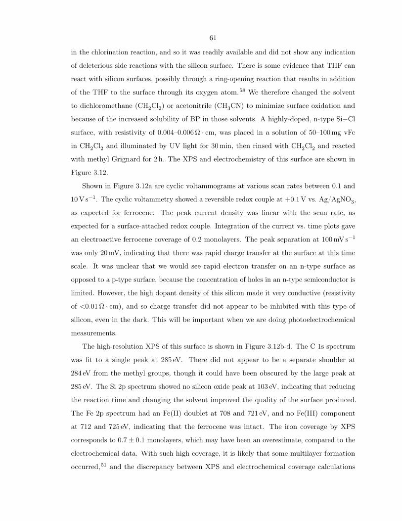
61
in the chlorination reaction, and so it was readily available and did not show any indication
of deleterious side reactions with the silicon surface. There is some evidence that THF can
react with silicon surfaces, possibly through a ring-opening reaction that results in addition
of the THF to the surface through its oxygen atom.58 We therefore changed the solvent
to dichloromethane (CH2Cl2) or acetonitrile (CH3CN) to minimize surface oxidation and
because of the increased solubility of BP in those solvents. A highly-doped, n-type Si−Cl
surface, with resistivity of 0.004–0.006Ω · cm, was placed in a solution of 50–100mg vFc
in CH2Cl2 and illuminated by UV light for 30min, then rinsed with CH2Cl2 and reacted
with methyl Grignard for 2 h. The XPS and electrochemistry of this surface are shown in
Figure 3.12.
Shown in Figure 3.12a are cyclic voltammograms at various scan rates between 0.1 and
10V s−1. The cyclic voltammetry showed a reversible redox couple at +0.1V vs. Ag/AgNO3,
as expected for ferrocene. The peak current density was linear with the scan rate, as
expected for a surface-attached redox couple. Integration of the current vs. time plots gave
an electroactive ferrocene coverage of 0.2 monolayers. The peak separation at 100mV s−1
was only 20mV, indicating that there was rapid charge transfer at the surface at this time
scale. It was unclear that we would see rapid electron transfer on an n-type surface as
opposed to a p-type surface, because the concentration of holes in an n-type semiconductor is
limited. However, the high dopant density of this silicon made it very conductive (resistivity
of <0.01Ω · cm), and so charge transfer did not appear to be inhibited with this type of
silicon, even in the dark. This will be important when we are doing photoelectrochemical
measurements.
The high-resolution XPS of this surface is shown in Figure 3.12b-d. The C 1s spectrum
was fit to a single peak at 285 eV. There did not appear to be a separate shoulder at
284 eV from the methyl groups, though it could have been obscured by the large peak at
285 eV. The Si 2p spectrum showed no silicon oxide peak at 103 eV, indicating that reducing
the reaction time and changing the solvent improved the quality of the surface produced.
The Fe 2p spectrum had an Fe(II) doublet at 708 and 721 eV, and no Fe(III) component
at 712 and 725 eV, indicating that the ferrocene was intact. The iron coverage by XPS
corresponds to 0.7± 0.1 monolayers, which may have been an overestimate, compared to the
electrochemical data. With such high coverage, it is likely that some multilayer formation
occurred,51 and the discrepancy between XPS and electrochemical coverage calculations
62
−0.2 0 0.2 0.4
−0.4
0
0.4
υ
Potential (vs. Ag/AgNO3)
Cur
rent
Den
sity
(mA
cm-2
)
280 285 290
Cou
nts
B. E. (eV) 97 101 105
Cou
nts
B. E. (eV)
702 717 732
Cou
nts
Binding Energy (eV)
a b c
d
C 1s Si 2p
Fe 2p
Figure 3.12: The electrochemistry and XPS of a mixed vFc/methyl surface produced byreaction with vFc in CH2Cl2 with BP, illuminated by UV light for 30min, followed by reactionwith methyl Grignard. a) Cyclic voltammetry showing the surface-attached ferrocene redoxcouple. Increasing scan rate from 0.1 to 10V s−1 is indicated by the black arrow. b) The highresolution C 1s XPS of the surface. This peak was fit to a single large peak around 285 eV,suggesting that any methyl peak at 284 eV was obscured by the large carbon componentfrom the ferrocene groups. c) The high-resolution Si 2p XPS of the surface, showing littleto no surface oxide peak at 103 eV. d) The high-resolution Fe 2p XPS showing the Fe(II)doublet at 708 and 721 eV, with little to no Fe(III) visible at 712 and 725 eV.

63
Solvent THF THF CH2Cl2 CH3CN CH3CNTime under UV 2 h 2 h 30 min 2 h 2 h
BP (y/n) no no yes yes yesMethyl (y/n) no yes yes no yes
Charge-carrier lifetime (ms) 0.02 0.37 0.38 0.05 0.40S (cm s−1) 870 48 46 350 43
ηFea 0.05 ± 0.02 0.01 ± 0.01 0.6 ± 0.1 0.3 ± 0.1 0.3 ± 0.1
acoverage of Fe per atop site determined by XPS.
Table 3.2: Properties of vFc-modified Cl-terminated Si surfaces using UV-light inducedreaction.
could be due to non-electroactive ferrocene sitting on the surface. This phenomenon has
been seen previously on vFc-modified silicon surfaces, where the surface coverage measured
using XPS was higher than the coverage measured electrochemically.47 Some of this ferrocene
could be non-electroactive because there was not a suitable pathway for the charges to reach
the redox center, or it could simply have fallen off the surface after immersion in electrolyte
because it was not actually covalently bound to the surface.
We wanted to ensure that the photoelectronic properties of these surfaces were not affected
by the addition of BP to the reaction solution or by changing the solvents. To this end, several
surfaces were prepared using intrinsically doped silicon under a variety of conditions for SRV
measurements. The results of these experiments are displayed in Table 3.2. All starting
surfaces were chlorine-terminated. The surfaces prepared using THF as the solvent, without
BP in solution, had low vFc surface coverage, as discussed above. The SRVs on these surfaces
that were not methylated with methyl Grignard were high, with S = 870 ± 50 cm s−1. When
these surfaces were methylated following reaction with vFc in THF, the SRVs were much
lower, with S = 48 ± 5 cm s−1. Changing the solvent to CH2Cl2 and adding BP to the vFc
solution greatly increased the vFc surface coverage, as discussed above. One surface modified
with vFc in CH2Cl2 with BP in solution under UV illumination for 30min, followed by
methylation with methyl Grignard, had S = 46 cm s−1. Several other surfaces functionalized
with vFc by illumination with UV light in CH2Cl2 with BP for between 20 and 180min,
followed by methylation, also had SRVs of between 40 and 70 cm s−1, depending on the time
spent under UV illumination (not shown in table). When CH3CN was used as the solvent,
surface coverage of vFc was also high, with the results shown in Table 3.2. For surfaces
prepared with vFc in CH3CN with BP under illumination for 2 h, surface coverage of Fe was
0.30± 0.05 monolayers. When these surfaces were methylated following UV illumination,
64
S = 43 ± 5 cm s−1, whereas when methylation did not occur, S = 350 ± 50 cm s−1. These
results made it clear that the addition of BP to the reaction solution and the use of CH2Cl2 or
CH3CN as the solvent did not adversely affect the photoelectronic properties of the surfaces.
Rather, using these solvents and adding BP to the reaction solution greatly increased the
surface coverage of vFc at moderate illumination times (30 to 120min) without adversely
affecting the photoelectronic properties of the surfaces.
3.4.3 Photoelectrochemistry
Photoelectrochemical experiments were carried out on silicon wafers with various levels of
doping, which changed the resistivity of the wafers. Details of the photoelectrochemistry
experiments can be found in Appendix B.4. We wanted to determine whether changing the
dopant density of the silicon would have an effect on the photovoltages or electron transfer rates
measured on these surfaces. Beginning with highly doped n+-Si(111), with resistivity 0.004–
0.006Ω · cm, we functionalized a series of silicon wafers with mixed methyl/vinylferrocenyl
monolayers and measured their photoelectrochemical properties. The results are summarized
in Table 3.3. There does not appear to be a clear correlation between dopant density and
photovoltage. Except for the highly doped sample (resistivity 0.004–0.006Ω · cm), all the
wafers generated photovoltages of 400± 50mV. The highly doped n-type silicon had a small
photovoltage of 50mV, suggesting that it may not actually be degenerate.
The charge transfer rates (ket) on the surfaces were measured using potential-step
chronoamperometry experiments.49 The details of these experiments and calculations can
be found in Appendix B.4.2. Independent measurements were made for the oxidation and
reduction reactions, allowing us to measure ket for both the oxidation (ket,ox) and reduction
(ket,red) of the vFc on the surface. These rates were measured both in the dark (ket,dark)
and under illumination (ket,light), allowing us to compare the efficacy of interfacial charge
transfer under these conditions. The relative magnitude of the charge transfer rate can also
be estimated using Epp, the peak-to-peak separation of the redox couple. For a surface
attached redox couple, Epp should be small, ideally zero. However, Epp will increase with
the scan rate if ket is comparable to the voltammetric time scale. A large Epp (>100mV)
indicates slower charge transfer, and small Epp (<50mV) indicates faster charge transfer,
on the timescale of the scan rate used for these experiments (100mV s−1 for the samples
described in Table 3.3).54

65
The charge transfer rate showed a moderate correlation with the dopant density of
the silicon wafers. The degenerately doped sample showed fast charge transfer (ket =
30± 10 s−1) and small Epp (20± 5mV) in the light and the dark, as one would expect for
a highly conductive sample. All other samples had low charge transfer rates for ferrocene-
oxidation in the dark (ket,ox,dark ≤5± 5 s−1), and fast charge transfer under illumination
(ket,light = 30± 10 s−1). Most interestingly, moderately doped n-type silicon (resistivity of
0.01–10Ω · cm) had fast ferrocenium-reduction kinetics in the dark (ket,red,dark = 20± 10 s−1).
This indicated that the ferrocenium-reduction reaction was not limited by electron availability
on these samples, though ferrocene-oxidation was limited by hole availability. However, for
samples with resistivity of >20Ω · cm, both ferrocene-oxidation and ferrocenium-reduction
were slow in the dark (ket,dark <5± 5 s−1), indicating that both electron and hole availability
were limiting factors for the charge transfer reaction. This agreed fairly well with predicted
behavior for n-type silicon.
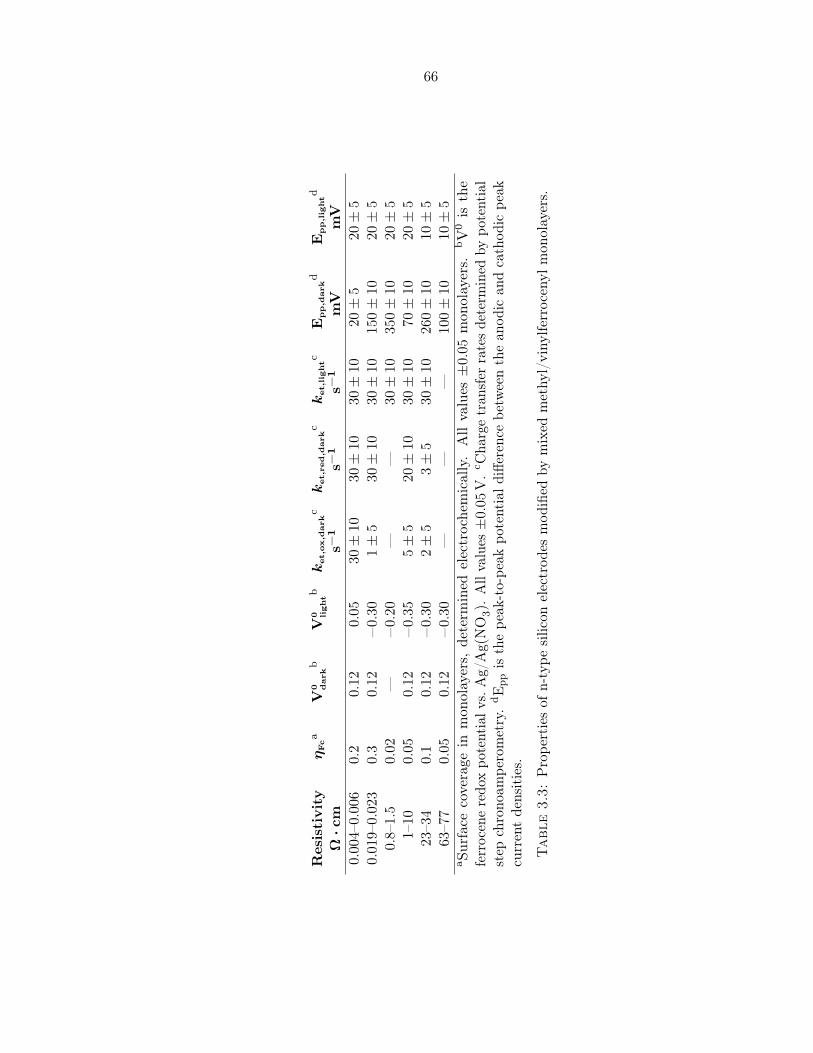
66
Resistivity
ηFca
V0 dar
kb
V0 lightb
ket
,ox,d
arkck
et,r
ed,d
arkc
ket
,lig
htc
Epp,d
arkd
Epp,lig
htd
Ω·cm
s−1
s−1
s−1
mV
mV
0.00
4–0.00
60.2
0.12
0.05
30±
1030
±10
30±
1020
±5
20±
50.01
9–0.02
30.3
0.12
−0.30
1±
530
±10
30±
1015
0±
1020
±5
0.8–
1.5
0.02
—−0.20
——
30±
1035
0±
1020
±5
1–10
0.05
0.12
−0.35
5±
520
±10
30±
1070
±10
20±
523
–34
0.1
0.12
−0.30
2±
53±
530
±10
260±
1010
±5
63–7
70.05
0.12
−0.30
——
—10
0±
1010
±5
a Surface
coverage
inmon
olayers,
determ
ined
electroche
mically.Allvalues
±0.05
mon
olayers.
bV
0is
the
ferrocen
eredo
xpo
tentialv
s.Ag/Ag(NO3).Allvalues
±0.05
V.c C
hargetran
sfer
ratesde
term
ined
bypo
tential
step
chrono
ampe
rometry.dEpp
isthepe
ak-to-pe
akpo
tentiald
ifferen
cebe
tweenthean
odic
andcathod
icpe
akcu
rrentde
nsities.
Tabl
e3.
3:Prope
rtiesof
n-type
silic
onelectrod
esmod
ified
bymixed
methy
l/viny
lferrocenyl
mon
olayers.

67
3.4.4 Stability Testing
While the surface-attached ferrocene was well behaved in non-aqueous solvents and at mod-
erate potentials under illumination, a water-splitting device will be used under quite different
conditions. Previous electrochemical experiments showed that mixed methyl/vinylferrocenyl
surfaces degraded rapidly at potentials more oxidizing than +0.4V vs. Fc/Fc+, resulting
in significant oxidation of the surface and loss of the ferrocene moiety. The silicon sur-
face, however, is predicted to be reductively stable. We tested this by cycling a mixed
methyl/vinylferrocenyl surface between +0.4 and −2.0V vs. Fc/Fc+ for an hour at a variety
of scan rates. The scan rate dependence of the peak current density was linear, indicating
that the ferrocene was surface-bound.49 Figure 3.13 shows the first and final CVs taken
on this surface. The scans were very similar, corresponding to 0.81± 0.05 and 0.74± 0.05
monolayers of ferrocene, respectively, indicating that the mixed monolayer is reductively
stable.
We also tested the stability of the surface under acidic conditions that would be used
for studies of proton reduction. We first soaked a mixed methyl/vinylferrocenyl surface in a
solution of 0.1M electrolyte and 40mM p-toluenesulfonic acid (tosic acid, Sigma, ≥98.5%)
in acetonitrile for 2 h to simulate model electrochemical conditions. XPS of the surface
before and after treatment resulted in a small decrease in iron coverage (0.08 monolayers
to 0.06 monolayers). This could indicate some acid instability, or could simply be due to
the additional handling, rinsing, and sonication to which the wafer was subjected after acid
treatment. Additionally, this experiment was performed under ambient conditions, and so
was exposed to oxygen from the air and in the solvent for the duration of the experiment.
To further explore the stability of the surface under acidic conditions, electrochemical
experiments were performed.
Figure 3.14 shows a series of cyclic voltammograms collected on a mixed methyl/ferrocenyl
surface as the acid concentration of the electrolyte solution was increased from 0 to 17mM
Tosic acid. This experiment was performed under inert atmospehere (N2) in nonaqueous
solvent (CH3CN, anhydrous). The shape and size of the ferrocene redox signal did not change
as the acid concentration was increased. Over the course of the experiment, the electroactive
ferrocene coverage on the surface remained essentially constant, with a decrease in ferrocene
coverage from the first to final scan of less than 0.01 monolayers. There was an increase

68
−2 −1 0−40
−20
0
20
40
First sweepLast sweep
Potential (vs. Fc/Fc+)
Cur
rent
Den
sity
(µA
cm-2
)
Figure 3.13: Cyclic voltammetry of a mixed methyl/vinylferrocenyl surface in acetonitrile.This surface is reductively stable to −2V vs. Fc/Fc+ with trace losses of electroactivematerial from the surface after an hour of cycling. In red, the first CV sweep performedon the surface. In blue, the final CV sweep performed on the surface. These two CVs arenearly identical, corresponding to 0.80± 0.05 and 0.75± 0.05 monolayers of surface-attachedferrocene, respectively.
−1 −0.5 0−4
−2
0
2
0 mM TsOH2 mM4 mM6 mM7 mM11 mM14 mM17 mM
Potential (vs. Fc/Fc+)
Cur
rent
Den
sity
(µA
cm-2
)
Figure 3.14: Cyclic voltammetry of a mixed methyl/vinylferrocenyl silicon surface underacidic conditions. This experiment was performed under inert atmosphere in anhydrousMeCN with 0.1M (NEt4)ClO4 as the electrolyte and Tosic acid (TsOH) as the proton source.The acid concentration was increased from 0 to 17mM and sequential CVs were collected ata scan rate of 100mV s−1.
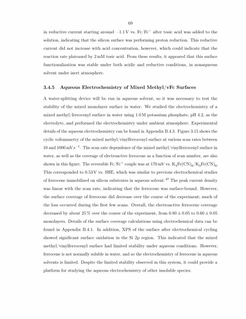
69
in reductive current starting around −1.1V vs. Fc/Fc+ after tosic acid was added to the
solution, indicating that the silicon surface was performing proton reduction. This reductive
current did not increase with acid concentration, however, which could indicate that the
reaction rate plateaued by 2mM tosic acid. From these results, it appeared that this surface
functionalization was stable under both acidic and reductive conditions, in nonaqueous
solvent under inert atmosphere.
3.4.5 Aqueous Electrochemistry of Mixed Methyl/vFc Surfaces
A water-splitting device will be run in aqueous solvent, so it was necessary to test the
stability of the mixed monolayer surface in water. We studied the electrochemistry of a
mixed methyl/ferrocenyl surface in water using 1.0M potassium phosphate, pH 4.2, as the
electrolyte, and performed the electrochemistry under ambient atmosphere. Experimental
details of the aqueous electrochemistry can be found in Appendix B.4.3. Figure 3.15 shows the
cyclic voltammetry of the mixed methyl/vinylferrocenyl surface at various scan rates between
10 and 1000mV s−1. The scan rate dependence of the mixed methyl/vinylferrocenyl surface in
water, as well as the coverage of electroactive ferrocene as a function of scan number, are also
shown in this figure. The reversible Fc/Fc+ couple was at 170mV vs. K4Fe(CN)6/K3Fe(CN)6.
This corresponded to 0.53V vs. SHE, which was similar to previous electrochemical studies
of ferrocene immobilized on silicon substrates in aqueous solvent.47 The peak current density
was linear with the scan rate, indicating that the ferrocene was surface-bound. However,
the surface coverage of ferrocene did decrease over the course of the experiment; much of
the loss occurred during the first few scans. Overall, the electroactive ferrocene coverage
decreased by about 25% over the course of the experiment, from 0.80± 0.05 to 0.60± 0.05
monolayers. Details of the surface coverage calculations using electrochemical data can be
found in Appendix B.4.1. In addition, XPS of the surface after electrochemical cycling
showed significant surface oxidation in the Si 2p region. This indicated that the mixed
methyl/vinylferrocenyl surface had limited stability under aqueous conditions. However,
ferrocene is not normally soluble in water, and so the electrochemistry of ferrocene in aqueous
solvents is limited. Despite the limited stability observed in this system, it could provide a
platform for studying the aqueous electrochemistry of other insoluble species.
70
0 0.2 0.4
−0.3
−0.2
−0.1
0
0.1
0.2
5 10 15 200
0.3
0.6
0.9
−0.5 0 0.5
−0.2
0
0.2
Cur
rent
Den
sity
(mA
cm-2
)
J (m
A cm
-2)
Potential (vs. K3Fe(CN)6/K4Fe(CN)6)
Scan Rate (V s-1)
Scan Number
η Fc (
mon
olay
ers)
υ a b
c
Figure 3.15: Electrochemistry of a mixed methyl/vinylferrocenyl surface in water. a) Cyclicvoltammetry of the surface from 10 to 1000mV s−1, with increasing scan rate indicated by theblack arrow. b) Peak current density as a function of scan rate, showing a linear dependenceas expected for a surface-attached redox couple. c) Surface coverage of electroactive ferroceneas a function of scan number. The surface coverage decreased from 0.80± 0.05 to 0.60± 0.05monolayers, which meant that approximately 25% of the ferrocene was lost from the surfaceover the course of the experiment.

71
3.5 Conclusion
Mixed methyl/vinylferrocene monolayers have been formed on Si(111) surfaces via a straight-
forward route. Our methodology has a potentially large substrate scope and applicability
to other redox-active molecules. The UV-light initiated reaction allowed us to dramatically
decrease the amount of vinylferrocene necessary for surface attachment, and the addition of
BP to the reaction solution drastically decreased the reaction time necessary for high surface
coverage. The electroactive surface coverage of the ferrocene in these mixed monolayers
could be varied from <1 to 100% of the silicon atop sites. The functionalized surfaces were
resistant to oxidation and permitted relatively rapid interfacial charge transfer to the attached
ferrocene group. The mixed monolayers maintained the favorable electronic properties of
the underlying silicon, as evidenced by the low surface recombination velocities measured
on the functionalized surfaces, as well as the 400± 50mV photovoltage generated on n-type
silicon. This method is therefore an attractive approach for the attachment of electrocata-
lysts and other functional groups to silicon surfaces, without introducing deleterious surface
recombination sites or chemical instability to the resulting Si/organic interface.
Portions of the preceding chapter have been adapted with permission from Lattimer et
al.34 Copyright 2013 American Chemical Society.
72
Chapter 4
Assembly, Characterization, andElectrochemical Properties ofImmobilized Metal BipyridylComplexes on Silicon(111) Surfaces
4.1 Introduction
The ability to prepare a catalyst-functionalized silicon surface that is free of both electronic
defects and chemically reactive sites will be a necessary development for the advancement of
any silicon-based solar-fuels device. If complex organometallic catalysts can be immobilized
on semiconductor-electrode surfaces without loss of catalytic activity, these assembled
photocathodes could perform reductive, fuel-forming reactions, such as the conversion of
protons to dihydrogen, or the reduction of CO2 to liquid fuels.59 60 61 Retaining the activity
of surface-bound molecular catalysts remains challenging due to the limited compatibility of
most molecular catalysts with conditions that are suitable for covalently attaching ligands
to the silicon surface.56 Furthermore, the proper coordination environment around the
metal center must be maintained during electrochemical cycling to prevent ligand-exchange
processes which may cause either the loss of catalyst molecules from the surface, or the
formation of secondary heterogeneous materials.62 63
We used the method for preparing mixed monolayers on Si(111) that combines the chlorine-
termination route with UV light-induced attachment of vinyl-tagged reagents discussed in
Chapter 3 to form a new class of mixed monolayers suitable for catalyst attachment, as shown
in Scheme 4.1. We used this method based on the structural similarity between vinylferrocene

73
Scheme 4.1: Route for formation of mixed methyl/vbpy monolayer. Reproduced bypermission of The Royal Society of Chemistry (RSC).64
OO
OORu
NN
+
ClRhNN
+
Cl-ClIrN
N
+
Cl-PF6-
NN
Fe
1 2
3 4 5
Figure 4.1: Structures of 1-5. 1) 4′-vinyl-2,2′-bipyridyl, vbpy. 2) vinylferrocene, vFc.3) [Cp*Rh(bipy)Cl]Cl. 4) [Cp*Ir(bipy)Cl]Cl. 5) [Ru(acac)2(bpy)]PF6. Reproduced bypermission of The Royal Society of Chemistry (RSC).64
(2) and 4′-vinyl-2,2′-bipyridyl (vbpy, 1, see Figure 4.1), which we anticipated would result
in similar reactivity with the silicon surface. The chlorinated surface (i.e., all atop sites
terminated as Si−Cl) was briefly exposed to CH3MgCl to yield a predominantly methyl-
terminated surface with some remaining unreacted Si−Cl bonds. This partially methylated
surface was then reacted with vbpy under UV light to produce a mixed methyl/vbpy
monolayer on the silicon surface. This surface was characterized and shown to display
good photoelectronic properties, low surface oxidation, and high bipyridine (bipy) coverages
(between 0.1 and 0.35 monolayers).
Using these surfaces, we subsequently demonstrated that this immobilized ligand can
form complexes with metal reagents on the surface. We assembled immobilized analogues of
pentamethylcyclopentadienyl (Cp∗) rhodium (3) and iridium (4) complexes of bipyridine, as
well as a ruthenium complex (5, Figure 4.1) on the surface. As the rhodium complexes have
been shown by Grätzel, Kölle, and others to serve as proton-reduction catalysts,65–70 we
investigated the stability of the Rh system in the presence of p-toluenesulfonic acid. Much of
the work discussed in this chapter was done in collaboration with Dr. James Blakemore.

74
Clacetonitrile
benzoyl peroxide254-nm light0.5-3 h
Cl
Si SiSi
NN
1.0 M, THF
2 h, 65 oC
CH3MgClCl
Si
4'-vinyl-2,2'-bipyridylCH3
SiSi
NN
Scheme 4.2: Initial route used for the formation of mixed vbpy/methyl monolayer.
4.2 Mixed Vinylbipyridyl/Methyl Surfaces
We formed our first mixed vinylbipyridyl/methyl monolayers by mimicking the reaction
sequence used for forming mixed methyl/vinylferrocenyl monolayers. This was done by
chlorinating a H−Si(111) surface, placing the wafer in a solution of vbpy in acetonitrile
(CH3CN) with benzoyl peroxide (BP) added as a radical initiator, and exposing it to UV
light for 30 to 180 min. The surface was then rinsed with CH3CN to remove residual reactant
and placed in 1 M CH3MgCl in THF at 60 C for 2 h. This reaction scheme is shown in
Scheme 4.2. Experimental details can be found in Appendix A.11. The surfaces formed by
this method had between 0.1 and 0.9± 0.1 monolayers of bipy and showed significant surface
oxidation. The surface coverage of silicon oxide and bipy for mixed monolayers prepared by
varying the reaction time with vbpy is shown in Table 4.1. Bipy coverage was quantified using
the N 1s signal, with two nitrogen atoms per bipy molecule. Details of the quantification
methodology can be found in Appendix B.1.1.
High-resolution XPS of a typical mixed vbpy/methyl surface formed using this reaction
sequence is shown in Figure 4.2. These mixed vbpy/methyl surfaces all had some surface
oxidation, as seen by the Si 2p peak at 103 eV. This peak increased in intensity with reaction
time in the vbpy solution under UV illumination. The C 1s region for all these surfaces had a
distinct peak at 284 eV, indicating that there are methyl groups on the surface, and a larger,
broader peak at 285 eV from the vbpy moiety on the surface, as well as adventitious carbon
contributions. The N 1s region of these surfaces had a single peak at 399.8 eV from the bipy
groups, indicating that the attachment of the vbpy group was successful. This nitrogen
signal increased with reaction time in the vbpy solution, indicating increased attachment of
vbpy to the surface.

75
282 286 290
Cou
nts
Binding Energy (eV) 97 101 105
Cou
nts
Binding Energy (eV) 395 400 405
Cou
nts
Binding Energy (eV)
Si 2p C 1s N 1s a b c
Figure 4.2: High-resolution XPS of a mixed vbpy/methyl surface. a) The Si 2p regionhad a small oxide peak at 103 eV. b) The C 1s region had a peak at 284 eV from the methylgroups and a larger components at 285 and 287 eV from the vbpy groups and adventitiouslyadsorbed carbon. c) The N 1s region had a single peak at 399.8 eV from the bipy groupsattached to the surface through the vinyl moiety.
CH3dichloromethane
10 mM, r.t., 1hSiSi
NN
CH3
SiSi
NN
RhCl
Cl-
[Cp*RhCl2]2
Scheme 4.3: Proposed reaction scheme for the ligation of [Cp∗RhCl2]2 by surface-boundbipy in a mixed vbpy/methyl monolayer.
4.2.1 Metallation with Rhodium Complexes
These surfaces were then metallated by submersion in a solution of 10mM [Cp∗RhCl2]2 in
dichloromethane (CH2Cl2) for 1 h, followed by sonication for 10min each in CH2Cl2, methanol
(CH3OH), and water. The proposed reaction scheme for the ligation of [Cp∗RhCl2]2 by
surface-bound bipy is shown in Scheme 4.3. [Cp∗RhCl2]2 was prepared following published
methods by J. Blakemore.71 These surfaces were then analyzed using XPS to quantify the
Rh that was bound to the surface through the bipy ligand. Table 4.1 shows the quantification
of selected elements for a series of mixed vbpy/methyl surfaces that were formed by varying
the time of exposure to vbpy under UV light. These surfaces were subsequently metallated
by [Cp∗RhCl2]2, and the amount of Rh bound to the bipy ligand is displayed in the table.
Details of the quantification methodology can be found in Appendix B.1.1.
Based on the surface coverages of >0.6 monolayers of bipy measured on some of the
surfaces, it is likely that multilayers of vbpy are forming. Bipy is a relatively large molecule

76
Reaction time in vbpy (min)30 60 120 180
mixed vbpy/methyl surfacesSi−O 0.2 ± 0.1 0.6 ± 0.1 0.9 ± 0.1 1.1 ± 0.1bipy 0.11± 0.05 0.16± 0.05 0.65± 0.05 0.85± 0.05
after reaction with [Cp∗RhCl2]Cl2Si−O 1.9 ± 1.0 1.9 ± 0.1 1.6 ± 0.1 1.6 ± 0.1bipy−Rh 0.17± 0.05 0.24± 0.05 0.25± 0.05 0.28± 0.05bipy-free 0.03± 0.01 — 0.39± 0.05 0.66± 0.05Rh 0.17± 0.05 0.21± 0.05 0.28± 0.05 0.33± 0.05
Table 4.1: Surface coverage in monolayers of selected elements on mixed vbpy/methylsurfaces, quantified by XPS. Si−O is the coverage of silicon oxide on the surface calculatedfrom the Si 2p peak at 103 eV. Bipy-free is the coverage of bipy on the surface calculatedfrom the N 1s peak at 399.8 eV. Bipy−Rh is the coverage of metallated bipy on the surfacecalculated from the N 1s peak at 400.7 eV. Rh is the coverage of Rh(III) on the surfacecalculated from the Rh 3d peaks at 310.1 and 314.8 eV.
and, like vFc, cannot fit on every Si atop site.51 This implies that there will be some bipy
that is buried or solvent-inaccessible, which could explain the relatively low coverage of Rh
(0.3 monolayers) measured on surfaces with high bipy coverage (0.9 monolayers). This is
further supported when comparing the surface coverage of Rh to the surface coverage of
metallated bipy (calculated from the N 1s peak at 400.7 eV). These values generally agree
within experimental error, suggesting that the N 1s component at 400.7 eV results from
Rh-ligated surface-attached bipy. The remaining unmetallated free-base bipy on the surfaces
is likely from surface-attached bipy that cannot be ligated by the Rh complex for steric
reasons. These multilayers of bipy may also explain why there was such a large Si−O signal
on these surfaces. It was possible that the methyl Grignard could not reach the surface to
react efficiently with the remaining Cl−Si sites on the surface, leaving them available for
surface oxidation after the wafers were removed from the flush box and exposed to atmosphere
and water during the cleaning procedure.
High-resolution XPS of a mixed vbpy/methyl surface metallated with Rh is shown in
Figure 4.3. The Si 2p region showed some surface oxidation, similar to the amount seen prior
to metallation (see Table 4.1). This indicated that the surface oxidation occurred during the
initial surface functionalization and not as a result of the metallation procedure. The N 1s
region was composed of two peaks, at 399.8 and 400.7 eV, corresponding to free-base and
bound bipy, respectively. The Rh 3d region had a doublet of peaks at 310.1 and 314.8 eV,

77
97 101 105
Cou
nts
Binding Energy (eV) 395 400 405
Cou
nts
Binding Energy (eV) 305 313 321
Cou
nts
Binding Energy (eV)
Si 2p N 1s Rh 3d a b c
Figure 4.3: High-resolution XPS of a mixed vbpy/methyl surface after metallation with[Cp∗RhCl2]2. a) The Si 2p region showed an increased silicon oxide peak at 103 eV aftermetallation. b) The N 1s region had two peaks, at 399.8 and 400.7 eV. The peak at 399.9 eVwas from free bipy on the surface, while the new peak at 400/7 eV was from metallated bipy.c) The Rh 3d region had a doublet of peaks at 310.1 and 314.8 eV, consistent with Rh(III).
with the 4.7 eV spit-orbit splitting and area ratio of 3:2 expected for a Rh 3d doublet. These
peak positions were consistent with rhodium in the +3 oxidation state, and were each fit
to a single component, indicating that there was a single species of rhodium on the surface.
In addition, [Cp∗Rh(bipy)Cl]Cl was prepared using published methods from [Cp∗RhCl2]2and bipy by J. Blakemore, and characterized by XPS.65 This Rh 3d region of this complex
consisted of a doublet of peaks at 310.1 and 314.8 eV with an area ratio of 3:2, which agreed
well with the Rh 3d region of our surface-attached complex.
4.2.2 Control Reactions
Several control experiments were performed to ensure that the rhodium was bound to the
surface through the bipy moiety, rather than nonspecifically adsorbed onto the surface.
Methyl-terminated silicon was immersed in a 10mM solution of [Cp∗RhCl2]2 in CH2Cl2 for
1 h, and then cleaned as described previously. XPS of this surface, shown in Figure 4.4,
revealed no rhodium or nitrogen signals. High-resolution XPS of the N 1s and Rh 3d regions
of the methyl surface also showed no above background signal, indicating that there was no
surface adsorption of the rhodium complex. Also shown in Figure 4.4 is a mixed methyl/vbpy
surface after metallation with [Cp∗RhCl2]]2. This surface had Rh 3d and N 1s signals at 312
and 400 eV, respectively, from the Rh-complex bound to the surface through the bipy ligand.
This implied that the bipy on the surface was necessary to bind the rhodium complex to the
surface.
A mixed methyl/vbpy surface was immersed in 20mM [Cp∗Rh(bipy)Cl]Cl (instead of
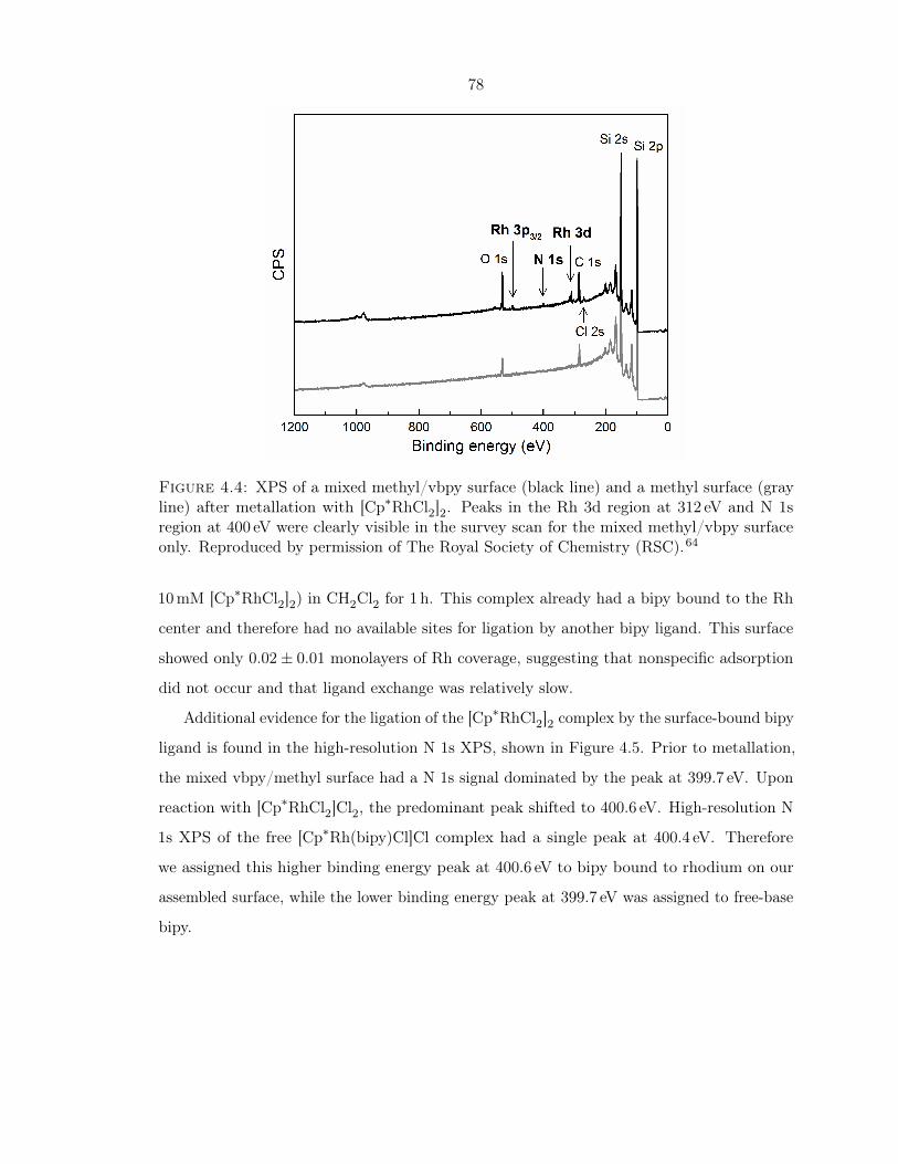
78
Figure 4.4: XPS of a mixed methyl/vbpy surface (black line) and a methyl surface (grayline) after metallation with [Cp∗RhCl2]2. Peaks in the Rh 3d region at 312 eV and N 1sregion at 400 eV were clearly visible in the survey scan for the mixed methyl/vbpy surfaceonly. Reproduced by permission of The Royal Society of Chemistry (RSC).64
10mM [Cp∗RhCl2]2) in CH2Cl2 for 1 h. This complex already had a bipy bound to the Rh
center and therefore had no available sites for ligation by another bipy ligand. This surface
showed only 0.02± 0.01 monolayers of Rh coverage, suggesting that nonspecific adsorption
did not occur and that ligand exchange was relatively slow.
Additional evidence for the ligation of the [Cp∗RhCl2]2 complex by the surface-bound bipy
ligand is found in the high-resolution N 1s XPS, shown in Figure 4.5. Prior to metallation,
the mixed vbpy/methyl surface had a N 1s signal dominated by the peak at 399.7 eV. Upon
reaction with [Cp∗RhCl2]Cl2, the predominant peak shifted to 400.6 eV. High-resolution N
1s XPS of the free [Cp∗Rh(bipy)Cl]Cl complex had a single peak at 400.4 eV. Therefore
we assigned this higher binding energy peak at 400.6 eV to bipy bound to rhodium on our
assembled surface, while the lower binding energy peak at 399.7 eV was assigned to free-base
bipy.
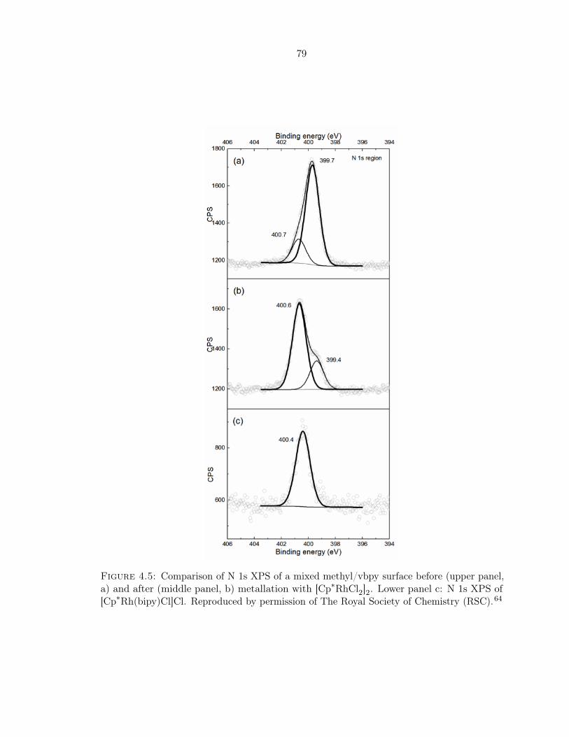
79
Figure 4.5: Comparison of N 1s XPS of a mixed methyl/vbpy surface before (upper panel,a) and after (middle panel, b) metallation with [Cp∗RhCl2]2. Lower panel c: N 1s XPS of[Cp∗Rh(bipy)Cl]Cl. Reproduced by permission of The Royal Society of Chemistry (RSC).64

80
5-60 min, 100oC
Cl
SiCl
Si Si
H
Si
PCl5, chlorobenzenebenzoyl peroxide
45-60 min, 90-100oC
N NRh
NCMe N
NRh
NCMe
(PF6)2
Scheme 4.4: Reaction sequence for the attachment of [Cp∗Rh(vbpy)CH3CN](PF6)2 toCl−Si(111).
4.2.3 Attachment of [Cp∗Rh(vbpy)CH3CN](PF6)2
In addition to metallation of the bound bipy ligand by Rh complexes, we simultaneously
pursued the direct attachment of the complete Rh catalyst to the surface. This was done using
the vinyl-tagged analog of the [Cp∗Rh(bipy)Cl]Cl species. [Cp∗Rh(vbpy)CH3CN](PF6)2 was
prepared by J. Blakemore using vbpy synthesized by W. Sattler. The chlorinated Si(111)
surface was reacted with this complex under UV light for 2 h in CH3CN with trace BP, as
shown in Scheme 4.4. Experimental details can be found in Appendix A.12.
Figure 4.6 shows the high-resolution XPS of [Cp∗Rh(vbpy)CH3CN](PF6)2 after attach-
ment to the silicon surface. The Si 2p region showed some surface oxidation at 103 eV,
corresponding to <1 monolayer of silicon oxide. The N 1s region had a predominant peak at
400.7 eV, corresponding to 0.35± 0.05 monolayers of nitrogen, with a shoulder at 399.8 eV,
corresponding to 0.06± 0.05 monolayers of nitrogen. This complex had three nitrogens bound
to the Rh center, and so 0.35 monolayers of nitrogen corresponds to 0.12± 0.03 monolayers of
the complex on the surface. The shoulder at 399.8 eV, corresponding to free-base bipy, could
be from vbpy that attached to the surface and subsequently lost its Rh center. The Rh 3d
region had two sets of doublets, at 308.5 and 312.8 eV and 310.5 and 315.1 eV. This indicates
that there were two kinds of Rh on the surface, most likely a Rh(I) and a Rh(III) species.
The Rh(III) is probably the same complex we have seen previously on similar surfaces, but
the Rh(I) species is unknown. The Rh(III) component, at 310.5 and 315.1 eV, corresponded
to 0.12± 0.02 monolayers, while the Rh(I) component, at 308.5 and 312.8 eV, corresponded
to 0.05± 0.02 monolayers. This agreed well with the quantification of the nitrogen signal.
There should be 12 F atoms per Rh atom (6 from each of the two PF–6 groups). Analysis of
the F 1s region gave 0.15± 0.05 monolayers, which corresponded to only 0.013 monolayers
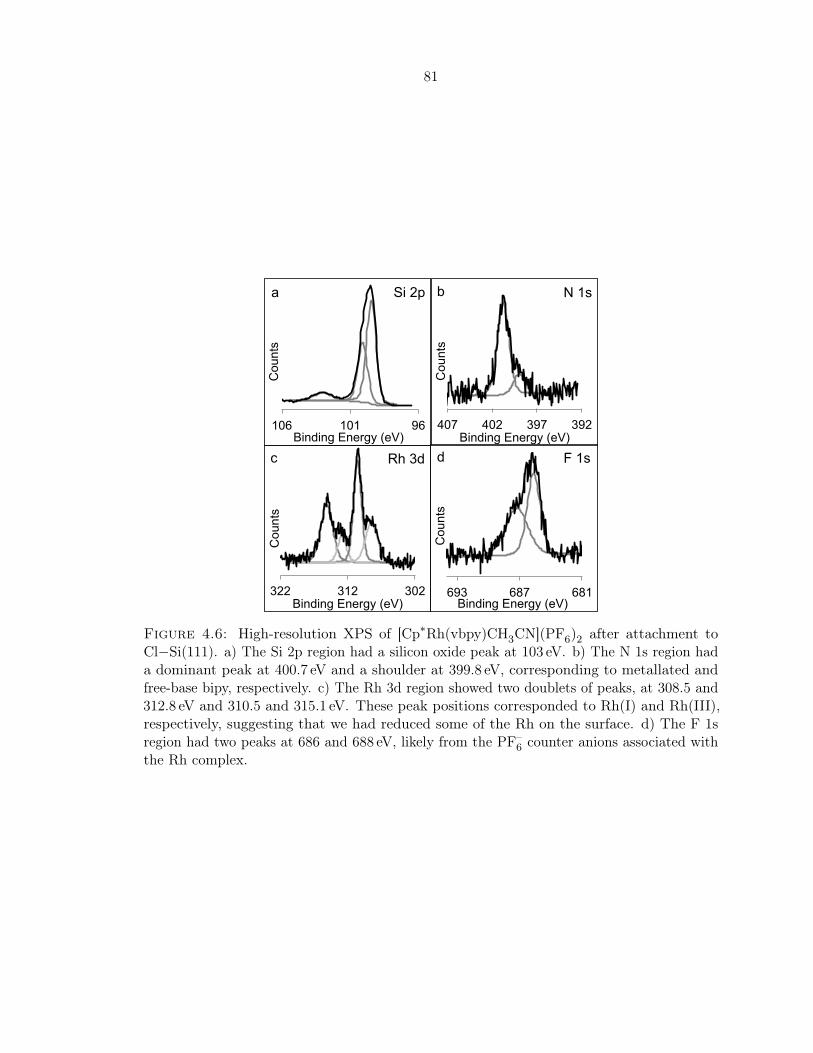
81
96 101 106
Cou
nts
Binding Energy (eV) 392 397 402 407
Cou
nts
Binding Energy (eV)
302 312 322
Cou
nts
Binding Energy (eV)
Si 2p N 1s
Rh 3d
a b
c
681 687 693
Cou
nts
Binding Energy (eV)
F 1s d
Figure 4.6: High-resolution XPS of [Cp∗Rh(vbpy)CH3CN](PF6)2 after attachment toCl−Si(111). a) The Si 2p region had a silicon oxide peak at 103 eV. b) The N 1s region hada dominant peak at 400.7 eV and a shoulder at 399.8 eV, corresponding to metallated andfree-base bipy, respectively. c) The Rh 3d region showed two doublets of peaks, at 308.5 and312.8 eV and 310.5 and 315.1 eV. These peak positions corresponded to Rh(I) and Rh(III),respectively, suggesting that we had reduced some of the Rh on the surface. d) The F 1sregion had two peaks at 686 and 688 eV, likely from the PF–
6 counter anions associated withthe Rh complex.

82
of complex. This indicated that the PF–6 anion was lost from the surface, possibly through
anion-exchange in solution, or because the complex has decomposed. Electrochemistry on
this surface was performed, but we did not observe any redox events. Our inability to see an
electrochemical signal for the redox couple on this surface suggested that decomposition may
be an issue.
4.3 Modification to Mixed Methyl/Vinylbipyridyl Monolayer
Formation
Our difficulty in preventing multilayer formation of the vbpy ligand and the significant surface
oxide observed on the resultant surfaces led us to modify the reaction sequence used to form
mixed methyl/vbpy monolayers. Following the reaction sequence shown in Scheme 4.1, we
first did a partial methylation of the Cl−Si(111) surface by immersing the wafer in 1M
CH3MgCl in THF at room temperature (r.t.) for 5min, followed by rinsing with THF. The
wafer was then placed in a solution of vbpy in CH2Cl2 with trace BP under UV illumination
for 1–2 h. Experimental details can be found in Appendix A.13.
This method resulted in better control over bipy surface coverage and lower surface
oxidation, as seen in Figure 4.7. The Si 2p region had no surface oxide, as evidenced by the
lack of a peak at 103 eV. The C 1s region had a broad peak at 285 to 288 eV with a small
shoulder at 284 eV, corresponding to carbon directly bound to silicon, assigned to the methyl
groups on the surface.29 13 The larger peak was a mixture of the carbon signals from the
vbpy group and any adventitious carbon on the surface. The N 1s region had a predominant
peak at 399.8 eV corresponding to 0.40± 0.05 monolayers of bipy, and a smaller shoulder at
400.7 eV corresponding to 0.13± 0.05 monolayers of bipy. The peak at 399.8 eV was from the
free bipy ligand on the surface, and the higher energy component was likely bipy metallated
by trace contaminants on the surface.
4.3.1 Metallation of Mixed Methyl/vbpy Surfaces with [Cp∗RhCl2]2
Having established a reproducible method of forming mixed methyl/vbpy surfaces with
low surface oxidation and high bipy coverage, metallation of the bipy ligand to form metal
complexes and catalysts on the surface could proceed. Mixed methyl/vbpy surfaces were
immersed in 10mM [Cp∗RhCl2]2 in CH2Cl2 for 1 h, with the results shown in Figure 4.8.

83
Cou
nts
105 102 99Binding Energy (eV)
Cou
nts
288 284Binding Energy (eV)
Si 2p C 1s N 1s a b c
Cou
nts
405 400 395Binding Energy (eV)
Figure 4.7: High-resolution XPS of a mixed methyl/vbpy surface. a) The Si 2p region didnot have a peak at 103 eV, indicating that the surface was not oxidized during the formationof this mixed monolayer. b) The C 1s region had a large, broad peak between 285 and 288 eV,with a distinct shoulder at 284 eV. c) The N 1s region had a predominant peak at 399.8 eVand a shoulder at 400.7 eV.
The Si 2p region did not have a surface oxide peak at 103 eV, indicating that the metallation
did not damage the surface. The N 1s region had a predominant peak at 400.7 eV and
a smaller peak at 399.6 eV, corresponding to metallated and free-base bipy, respectively.
Quantification of these peaks gave 0.40± 0.05 monolayers of metallated bipy and 0.13± 0.05
monolayers of free-base bipy. The Rh 3d region showed a doublet of peaks at 310.1 and 314.8
eV, each fit to a single component which corresponded to 0.5± 0.1 monolayers. The peak
positions were consistent with Rh(III) and agreed well with the values seen previously for the
[Cp∗Rh(bipy)Cl]Cl complex in XPS. The amount of Rh and metallated bipy measured on
this surface agreed within experimental error, suggesting that the complex was intact on the
surface. In addition, there was a distinct Cl 2s peak visible in the survey and high-resolution
Cl 2s spectra (not shown), indicating that the inner-sphere Cl– ligand and outer-sphere Cl–
anion remained bound to the surface with the complex. The C 1s spectrum (not shown) still
had a small shoulder at 284 eV from the methyl groups, but the signal was dominated by
a broad peak at 286 eV which contained the carbon signals from the bipy groups and the
metal complex, as well as any adventitious carbon on the surface.
4.3.2 Charge-Carrier Lifetimes of Mixed Methyl/vbpy Surfaces
Intrinsically-doped silicon was used to form mixed methyl/vbpy surfaces for SRV experiments.
The experimental details of the SRV set-up can be found in Appendix B.3. On a mixed
methyl/vbpy surface, the charge-carrier lifetime was 0.38± 0.01 ms, corresponding to an
SRV of 46± 5 cm s−1. This compared well to a methylated silicon surface, prepared and

84
Cou
nts
105 102 99Binding Energy (eV)
Cou
nts
320 312 304Binding Energy (eV)
Si 2p N 1s Rh 3d a b c
Cou
nts
405 400 395Binding Energy (eV)
Figure 4.8: High-resolution XPS of a mixed methyl/vbpy surface after metallation with[Cp∗RhCl2]2. a) The Si 2p region did not have a peak at 103 eV, indicating that the surfacewas not oxidized during metallation. b) The N 1s region had a predominant peak at 400.7 eVwith a shoulder at 399.6 eV, corresponding to metallated and free-base bipy, respectively. c)The Rh 3d region contained a doublet of peaks at 310.1 and 314.8 eV, consistent with Rh(III).These peaks were each fit to a single component, suggesting that we have one Rh(III) specieson the surface.
measured simultaneously for comparative purposes. The methylated silicon surface had a
charge-carrier lifetime of 0.77± 0.01 ms, corresponding to an SRV of 23± 5 cm s−1. The
mixed methyl/vbpy was metallated with [Cp∗RhCl2]2 and had a charge-carrier lifetime of
0.43± 0.01 ms, corresponding to an SRV of 41± 5 cm s−1. These numbers were all well
below the 100 cm s−1 limit indicative of good photoelectronic properties for Si(111) surfaces,
implying that these surfaces had good photoelectrochemical properties.
4.3.3 Electrochemistry of Surface-Bound [Cp∗Rh(bipy)Cl]Cl
Electrochemistry of the rhodium complexes was carried out in a N2-purged glovebox. All
solvents were anhydrous and all materials were furnace-dried before being brought into
the box. These experiments were carried out using 0.10M (NBu4)PF6 in CH3CN as the
electrolyte solution. Experimental details can be found in Appendix B.4.
In acetonitrile solution, [Cp∗Rh(bipy)Cl]Cl undergoes a chemically-reversible net two-
electron reduction from the starting rhodium(III) state to form a low-valent rhodium(I)
complex with loss of coordinated counterions or solvent.62,72 This complex shows a well-
behaved, reversible redox couple near −1.2V vs. Fc/Fc+, with basal-plane graphite as the
working electrode, shown in Figure 4.9. A plot of the peak current density vs. the square
root of the scan rate is linear, as expected for a freely-diffusing redox couple in solution.49
Similar CVs were collected using methyl-terminated silicon as the working electrode, with a
small shift in the redox couple to −1.1V vs. Fc/Fc+.

85
Figure 4.9: Solution Electrochemistry of [Cp∗Rh(bipy)Cl]Cl. Reproduced by permission ofThe Royal Society of Chemistry (RSC).64
Figure 4.10: Electrochemistry of a mixed methyl/vbpy surface after metallation with[Cp∗RhCl2]2. Reproduced by permission of The Royal Society of Chemistry (RSC).64

86
Figure 4.11: Electrochemistry of surface-attached [Cp∗Rh(bipy)Cl]Cl scanned over a limitedpotential range, from −0.2 to −1.3V vs. Fc/Fc+. An unmetallated mixed methyl/vbpysurface is shown in gray for comparative purposes. This suface did not display any redoxactivity at potentials more positive than −1.4V vs. Fc/Fc+. Reproduced by permission ofThe Royal Society of Chemistry (RSC).64
Figure 4.10 shows the first three cyclic voltammograms collected on a mixed methyl/vbpy
surface metallated by [Cp∗RhCl2]2. There was a redox couple at −1.0V vs. Fc/Fc+ with a
peak-to-peak separation of 10mV. This small peak separation was indicative of a surface-
bound, non-diffusive redox couple.49 The couple at −1.0V vs. Fc/Fc+ was consistent with the
solution electrochemistry of [Cp∗Rh(bipy)Cl]Cl. On the very first voltammetric scan from
−0.4 to 1.5V, there was background current flow in a second redox process around −1.3V
(possibly reduction of free bipyridine). On the return anodic scan, there was a non-diffusional
wave near −1V. Upon continued cycling, the current flow in the key redox process decreased
precipitously, suggesting that the species was lost from the electrode surface during cycling.
On the fourth and subsequent cycles, very low above-background current was visible. If the
scan limits were changed such that the potential was scanned only from −0.2 to −1.3V,
the observed process was more stable and was observed for up to six complete cycles of
voltammetry (see Figure 4.11). This figure also shows a CV collected on an unmetallated
mixed methyl/vbpy surface, for comparative purposes. This surface did not show any redox
activity prior to the free-base bipy reduction at −1.4V vs. Fc/Fc+.
The surface coverage of electroactive Rh was estimated to be 0.002± 0.001 of a monolayer

87
using integrated current-time data from the cyclic voltammetry (averaging both the anodic
and cathodic currents over three complete cycles). Details of this surface coverage calculation
can be found in Appendix B.4.1. This was only ∼1% of the coverage estimated from the
XPS data (0.21 monolayers), suggesting that not all of the metal present on the surface
was electroactive. The XP spectra collected after electrochemical cycling for the Rh-treated
mixed surface showed no signal in the Rh 3d region and a trace nitrogen signal in the N 1s
region. This indicated that both rhodium and bipyridine were lost from the surface upon
redox cycling. Notably, when the mixed surface was run reductively without metallation,
bipyridine was lost from that surface as well. Thus, the mechanism of loss of bipyridine from
the surface was not necessarily metal-catalyzed but rather occurred independently of the
presence of metal when the surface was cycled reductively. This reductive instability was in
marked contrast to mixed methyl/vFc surfaces, which were stable to −2V vs. Fc/Fc+ (see
Figure 3.13), suggesting that the reduction of the bipy ligand itself may play some role in
this instability.
4.3.4 Electrocatalysis of [Cp∗Rh(bipy)Cl]Cl
Despite the apparent loss of electroactive Rh from our surfaces upon reductive cycling,
catalytic reduction of protons to hydrogen could still occur. In solution, addition of p-
toluenesulfonic acid (tosic acid) to a solution of [Cp∗Rh(bipy)Cl]Cl results in loss of re-
versibility of the redox couple and an increase in the reductive current, corresponding to
catalysis. This is shown in Figure 4.12.
Addition of tosic acid to our surface-attached [Cp∗Rh(bipy)Cl]Cl should result in the
same reductive current at −1.0V vs. Fc/Fc+. In fact, we do see this catalytic current on a
mixed methyl/vbpy surface metallated with Rh. This surface was previously cycled between
−0.4 and −1.5V vs. Fc/Fc+ several times, resulting in loss of the redox event. However,
when tosic acid was added to the electrochemical cell, a reductive event starting at −1.0V
vs. Fc/Fc+ was observed. Figure 4.13 shows the reductive events on both a fresh mixed
methyl/vbpy surface and a Rh-metallated mixed methyl/vbpy surface. The silicon wafer
itself was catalytic for proton reduction at sufficiently negative potentials, as seen on the
mixed methyl/vbpy surface. However, the onset of catalysis occurred at a less negative
potential on the metallated surface, and the catalytic current was larger, suggesting that the
Rh complex was doing above-background proton reduction catalysis on this surface. The
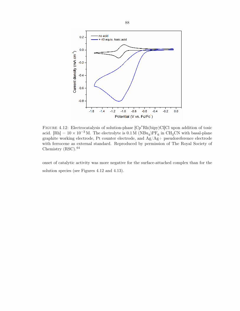
88
Figure 4.12: Electrocatalysis of solution-phase [Cp∗Rh(bipy)Cl]Cl upon addition of tosicacid. [Rh] = 10× 10−3M. The electrolyte is 0.1M (NBu4)PF6 in CH3CN with basal-planegraphite working electrode, Pt counter electrode, and Ag/Ag+ pseudoreference electrodewith ferrocene as external standard. Reproduced by permission of The Royal Society ofChemistry (RSC).64
onset of catalytic activity was more negative for the surface-attached complex than for the
solution species (see Figures 4.12 and 4.13).

89
Fig
ure
4.13
:Electrocatalysison
surface-bo
und[C
p∗Rh(vb
py)C
l]Clu
ponad
dition
oftosicacid.Le
ftpa
nel:
Backg
roun
delectrocatalysis
observed
onamixed
methy
l/vb
pysurfacein
thepresen
ceof
increasing
tosicacid
conc
entration.
Right
panel:
Abo
ve-backg
roun
delectrocatalysis
observed
onamixed
methy
l/vb
pysurfacemetallatedwith[C
p∗RhC
l 2] 2
withincreasing
tosicacid
concentration.
Dotted
lineis
hydrogen
redu
ctioncatalysiswithaPtwireworking
electrod
e.The
electrolyteis
0.1M
(NBu 4)P
F6in
CH3C
Nwithba
sal-p
lane
grap
hite
coun
terelectrod
e,an
dAg/
Ag+
pseu
doreferenceelectrod
ewithferroceneas
external
stan
dard.

90
We tested whether the Rh complex responsible for the above background catalytic activity
observed on the Rh-metallated mixed methyl/vbpy surface had fallen off the surface and
into solution. This was done by removing the electrolyte from the electrochemical cell
and rinsing the cell and working electrode with clean electrolyte solution, then refilling the
cell with fresh electrolyte solution with 0.723mM tosic acid added. Figure 4.14 shows the
electrocatalytic behavior observed on the Rh-metallated mixed methyl/vbpy surface before
and after replacing the electrolyte solution. As can be seen clearly in the figure, the catalytic
current was the same in both scans. This implied that the catalytic species was surface
bound.
4.3.5 Metallation of Mixed Methyl/vbpy Surfaces with [Cp∗IrCl2]2
Mixed methyl/vbpy surfaces were metallated by submersion in 10mM [Cp∗IrCl2]2 in CH2Cl2for 1 h at r.t. in air. They were then rinsed with CH2Cl2 to remove excess reagent and sonicated
sequentially in CH2Cl2, CH3OH, and water prior to characterization. [Cp∗IrCl2]2 was
prepared following published methods by J. Blakemore.71 These surfaces were characterized
by XPS, with the results shown in Figures 4.15 and 4.16. The survey scan showed new peaks
for Ir 4f at 65 eV, Ir 4d at 307 eV, and Ir 4p at 498 eV, in addition to the usual Si 2p, Si 2s,
C 1s, O 1s, N 1s, and Cl 2p and 2s signals.
The Si 2p region had a small peak at 103 eV, indicating that the surface was not
significantly oxidized during the metallation process. The surface oxide was quantified
and increased from 0.13± 0.05 monolayers to 0.21± 0.05 monolayers upon metallation, an
insignificant increase. The Ir 4f region consisted of a doublet of peaks at 62.9 and 65.9 eV,
each fit to a single component, with an area ratio of 4:3, as expected for a 4f peak. This peak
corresponded to 0.34± 0.05 monolayers of Ir. This matched well with the Ir 4f XP spectra
obtained for the model compound [Cp∗Ir(bpy)Cl]Cl (synthesized according to literature
procedures by J. Blakemore), which exhibited peaks at 62.9 and 65.9 eV.73
The N 1s region showed three contributions: a large peak at 400.8 eV, a smaller peak
at 399.6 eV, and a small peak (visible as a minor shoulder) at 402.2 eV. For comparison,
the model compound [Cp∗Ir(bipy)Cl]Cl showed a single N 1s peak at 400.7 eV, and so
the dominant peak at 400.8 eV for the metallated surface corresponded to iridium-bound
bipyridine on the surface, while the signal at 399.6 eV matched well with that for metal-free
immobilized bipyridine. These peaks corresponded to 0.17± 0.05 monolayers of metallated
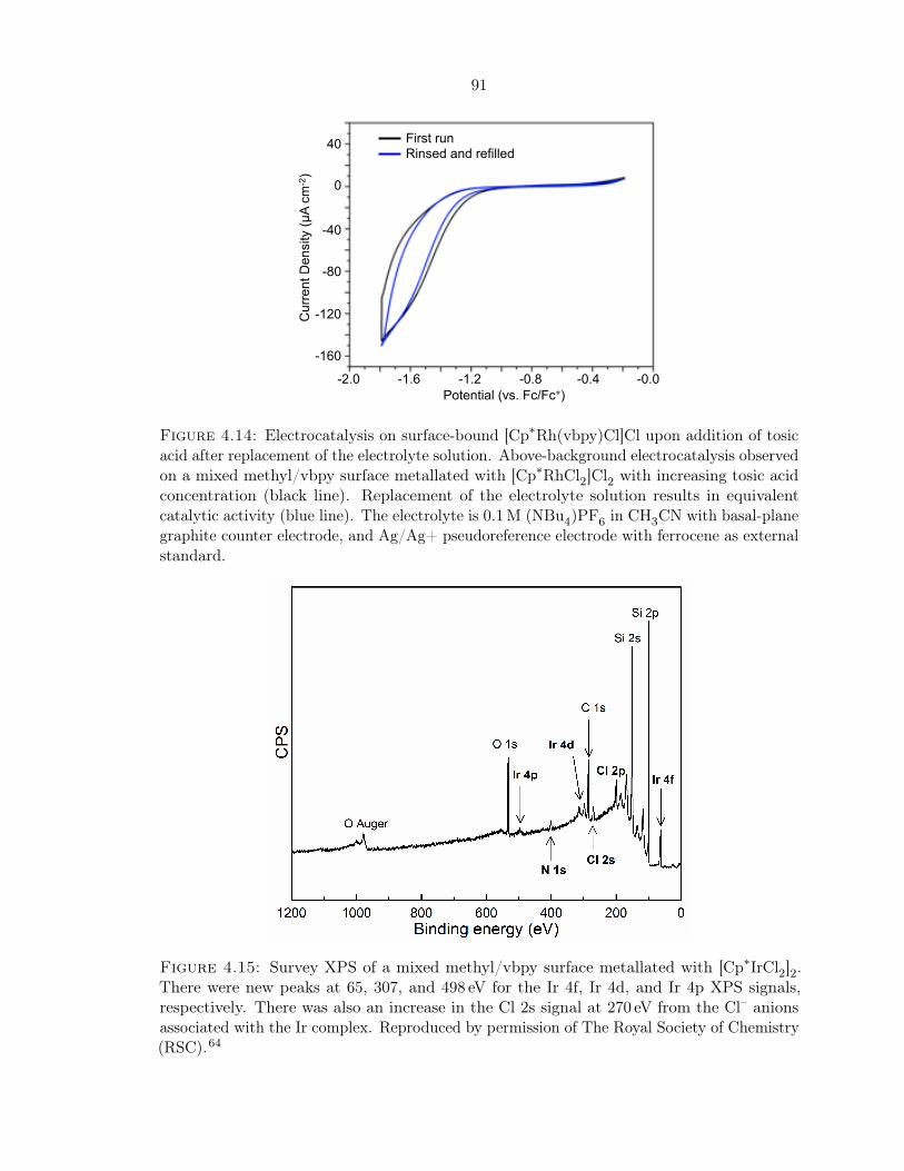
91
First run Rinsed and refilled
Cur
rent
Den
sity
(µA
cm-2
)
40
0
-40
-80
-120
-160
-2.0 -1.6 -1.2 -0.8 -0.4 -0.0 Potential (vs. Fc/Fc+)
Figure 4.14: Electrocatalysis on surface-bound [Cp∗Rh(vbpy)Cl]Cl upon addition of tosicacid after replacement of the electrolyte solution. Above-background electrocatalysis observedon a mixed methyl/vbpy surface metallated with [Cp∗RhCl2]Cl2 with increasing tosic acidconcentration (black line). Replacement of the electrolyte solution results in equivalentcatalytic activity (blue line). The electrolyte is 0.1M (NBu4)PF6 in CH3CN with basal-planegraphite counter electrode, and Ag/Ag+ pseudoreference electrode with ferrocene as externalstandard.
Figure 4.15: Survey XPS of a mixed methyl/vbpy surface metallated with [Cp∗IrCl2]2.There were new peaks at 65, 307, and 498 eV for the Ir 4f, Ir 4d, and Ir 4p XPS signals,respectively. There was also an increase in the Cl 2s signal at 270 eV from the Cl– anionsassociated with the Ir complex. Reproduced by permission of The Royal Society of Chemistry(RSC).64

92
Cou
nts
105 102 99 96Binding Energy (eV)
Cou
nts
70 65 60Binding Energy (eV)
Cou
nts
404 400 396Binding Energy (eV)
Si 2p N 1s Ir 4f a b c
Figure 4.16: High res XPS of a mixed methyl/vbpy surface metallated with [Cp∗IrCl2]2.a) The Si 2p region showed a small surface oxide contribution at 103 eV, indicating thatthe surface was slightly oxidized by the metallation procedure. b) The N 1s region had apredominant peak at 400.8 eV, corresponding to metallated bipy. There was also a smallshoulder at 399.6 eV, corresponding to free-base bipy, and an unassigned shoulder at 402.2 eV.c) The Ir 4f region had a doublet of peaks at 62.9 and 65.9 eV, each of which was fit to asingle component. This indicates that there is a single Ir species on the surface.
bipy and 0.07± 0.05 monolayers of free-base bipy, respectively.
Ir LIII-edge X-ray absorption spectroscopy (XAS) provided further evidence for assembly
of the desired complex on the surface. In Figure 4.17, the edge and post-edge data are
shown for a powder of isolated [Cp∗Ir(bipy)Cl]Cl (black line), while the data for analogous
immobilized [Cp∗Ir(vbpy)Cl]Cl are shown in blue circles. The iridium in both cases was
characterized by a peak-top energy of 11 215 eV. These edge-energy values were consistent
with iridium in the +3 oxidation state. In addition, the post-edge features were similar for
[Cp∗Ir(bipy)Cl]Cl and the silicon-immobilized analogue, suggesting a similar environment in
the first coordination shell for the iridium centers in both cases. These spectra were collected
with J. Blakemore at the Stanford Synchrotron Radiation Lightsource (SSRL) at the SLAC
National Accelerator Laboratory in Menlo Park, CA with the generous assistance of S. Gul,
R. Chatterjee, V. Yachandra, and J. Yano. Experimental details of the XAS experiments
can be found in Appendix B.5.
4.3.6 Metallation of Mixed Methyl/vbpy Surfaces with Ru(acac)2(coe)2
The reductive instability displayed by the surface-attached [Cp∗Rh(vbpy)Cl]Cl led us to
study a less reductive couple on the surface. [Ru(acac)2(bipy)]PF6 (acac is acetylacetonate)
was prepared and displayed a well-behaved, one-electron Ru(II)/Ru(III) couple at −0.5V vs.
Fc/Fc+, where the mixed methyl/vbpy surface should be stable (see Figure 4.19).74 Addition
of 2,2´-bipyridyl to Ru(acac)2(coe)2 (coe is cis-cyclooctene) gives Ru(acac)2(bipy) at r.t.75

93
Figure 4.17: Comparison of Ir LIII-edge XAS results for the mixed methyl/vbpy surfaceexposed to [Cp∗IrCl2]2 (blue circles) and the [Cp∗Ir(bipy)Cl]Cl model complex (black line).Reproduced by permission of The Royal Society of Chemistry (RSC).64
We wanted to form the oxidized version of this complex on the mixed methyl/vbpy surface.
However, the Ru(III) species, [Ru(acac)2(bipy)]PF6, could only be prepared at elevated
temperature in solution.74,76 To prepare a Ru-metallated surface, a mixed methyl/bipyridyl-
functionalized Si(111) sample was immersed in a ∼6mM solution of Ru(acac)2(coe)2 in THF
under Ar gas and heated to 100 C overnight in a sealed pressure vessel. This reaction was
first attempted at r.t., but it did not proceed. Following the reaction, the pressure vessel
was opened to room air after cooling, presumably resulting in oxidation of Ru(II) to Ru(III),
and the samples were then sonicated for 10min each in CH2Cl2, CH3OH, and water prior to
surface characterization.
High-resolution XPS of the surface after metallation with Ru(acac)2(coe)2 is shown in
Figure 4.18. The Si 2p region showed a small oxide peak at 103 eV, corresponding to 0.6± 0.1
monolayers. The wafer was subjected to rather harsh conditions (refluxing overnight in THF),
and so an increase in surface oxidation was not unexpected. The Ru 3p region showed a
doublet of peaks at 463.2 and 485.4 eV, each fit to a single component. These peak positions
corresponded to Ru(III), and agreed well with the Ru 3d peaks observed at 463.3 and 485.6 eV
for [Ru(acac)2(bipy)]PF6. These peaks had an area ratio of 2:1, as expected for a 3p doublet
in XPS. The Ru 3d peak corresponded to 0.21± 0.05 monolayers of Ru on the surface.
The N 1s region had a dominant signal at 400.5 eV and a smaller peak at 399.6 eV,

94
Cou
nts
104 100 96Binding Energy (eV)
Cou
nts
490 480 470 460Binding Energy (eV)
Si 2p N 1s Ru 3p a b c
Cou
nts
404 400 396Binding Energy (eV)
Figure 4.18: High-resolution XPS of the mixed methyl/vbpy surface exposed toRu(acac)2(coe)2 by refluxing at 100 C overnight in THF. a) The Si 2p region had a smalloxide peak at 103 eV. b) The N 1s region had a dominant peak at 400.5 eV and a shoulder at399.6 eV, corresponding to metallated and free-base bipy respectively. c) The Ru 3p regionhad a doublet of peaks at 363.2 and 485.4 eV, each fit to a single component, indicating thatthere was one Ru species on the surface.
corresponding to 0.26± 0.05 and 0.06± 0.02 monolayers, respectively. The model complex
[Ru(acac)2(bipy)]PF6 had a N 1s signal at 400.5 eV, and so we assigned the peak at 400.5 eV
to metallated bipy and the peak at 399.6 eV to free-base bipy. These coverages agreed well,
indicating that the Ru complex was intact on the surface. The counter-ion that should be
associated with this complex in the Ru(III) oxidation state is, however, unknown. While
no explicit counter ions were added to the reaction mixture, the total amount of the Ru
complex on the surface is quite low, and so trace anionic species in the reaction solution or
rinsing solvents could have become associated with the complex to balance the charges.
4.3.7 Electrochemistry of Surface-Bound [Ru(acac)2(bipy)]+
The ruthenium complex [Ru(acac)2(bipy)]PF6 underwent a single one-electron transfer,
cycling between the +3 and +2 oxidation states, at around −0.48V vs. Fc/Fc+ (Fig-
ure 4.19, upper panel) in a well-behaved, chemically reversible redox process. Similarly to
[Cp∗Rh(bipy)Cl]Cl, this complex showed the expected square-root dependence of peak cur-
rent on scan rate (see Figure 4.9). Redox cycling of surface-attached [Ru(acac)2(vbpy)]+ was
performed using mixed methyl/vbpy surfaces metallated with Ru(acac)2(coe)2 (Figure 4.19,
lower panel). We observed a redox couple on this surface with the half-wave potential
centered at −0.49V vs. Fc/Fc+, and with a peak-to-peak separation of 171mV. Details
of the electrochemical setup can be found in Appendix B.4. The peak-to-peak separation
of model complex [Ru(acac)2(bpy)]PF6 in solution was 71mV, suggesting slower electron

95
Figure 4.19: Comparison of the electrochemistry of [Ru(acac)2(bipy)]PF6 (upper panel) andthe mixed methyl/vbpy surface metallated with Ru(acac)2(coe)2 (lower panel). These CVswere collected in 0.1M (NBu4)PF6) in CH3CN, with a Ag/Ag+ pseudoreference electrodeand a basal-plane graphite counter electrode. The electrochemistry of the solution-phase[Ru(acac)2(bipy)]PF6 was collected on a basal-plane graphite working electrode. The scanrate in both cases was 100mV s−1. Reproduced by permission of The Royal Society ofChemistry (RSC).64

96
Cou
nts
104 100 96Binding Energy (eV)
Cou
nts
404 400 396Binding Energy (eV)
Si 2p Ru 3p a c N 1s b
Cou
nts
490 480 470 460Binding Energy (eV)
Figure 4.20: High-resolution XPS of the mixed methyl/vbpy surface exposed toRu(acac)2(coe)2 following electrochemical cycling. a) The Si 2p region had an oxide peakat 103 eV. b) The N 1s region had a dominant peak at 400.5 eV and a shoulder at 399.6 eV,corresponding to metallated and free-base bipy, respectively. There was also a small peak at402.2 eV that remains unassigned at this time. c) The Ru 3p region had a doublet of peaks at363.2 and 485.4 eV, each fit to a single component, indicating that there was one Ru specieson the surface. The amount of Ru on the surface decreased following electrochemical cycling,as is consistent with the loss of some electroactive material from the surface.
transfer to the immobilized complex than for the solution complex. While this redox couple
persisted beyond ten complete cycles of voltammetry from −0.2 to −0.9V, the redox couple
was not sufficiently long-lived to allow more extensive characterization. Integration of the
current-time data gave 0.002± 0.001 of a monolayer of electroactive ruthenium on the surface,
similar to the case of the rhodium complex discussed above.
The XP spectra of the ruthenium-treated electrode collected following the electrochemical
cycling indicated that some of the attached complex remained on the surface. This data
is shown in Figure 4.20. Before electrochemical cycling, the surface coverage of ruthenium
was 0.21± 0.05 monolayers, in good agreement with the estimated 0.26± 0.05 monolayers
of metal-bound bipy based on the N 1s signal; the coverage of silicon oxide was 0.6± 0.1
monolayers, and the coverage by free-base bipy was estimated as 0.06± 0.02 monolayers.
Following electrochemistry, the apparent coverage of silicon oxide increased slightly to
0.75± 0.10, while the free-base bipy coverage was essentially invariant at 0.05± 0.02. The
metal-bound bipy coverage dropped slightly to 0.22± 0.05 monolayers, and the ruthenium
coverage dropped to 0.11± 0.05. The decreases in metal-bound bipy and Ru coverages were
thus consistent with the eventual loss of the electrochemical signal. However, the lack of
electroactivity of the remaining material suggested nonideal interfacial electron transfer.
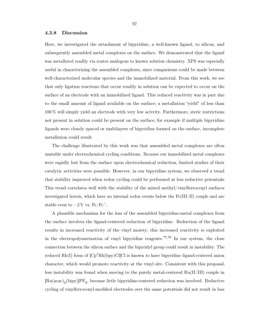
97
4.3.8 Discussion
Here, we investigated the attachment of bipyridine, a well-known ligand, to silicon, and
subsequently assembled metal complexes on the surface. We demonstrated that the ligand
was metallated readily via routes analogous to known solution chemistry. XPS was especially
useful in characterizing the assembled complexes, since comparisons could be made between
well-characterized molecular species and the immobilized material. From this work, we see
that only ligation reactions that occur readily in solution can be expected to occur on the
surface of an electrode with an immobilized ligand. This reduced reactivity was in part due
to the small amount of ligand available on the surface; a metallation “yield” of less than
100% will simply yield an electrode with very low activity. Furthermore, steric restrictions
not present in solution could be present on the surface; for example if multiple bipyridine
ligands were closely spaced or multilayers of bipyridine formed on the surface, incomplete
metallation could result.
The challenge illustrated by this work was that assembled metal complexes are often
unstable under electrochemical cycling conditions. Because our immobilized metal complexes
were rapidly lost from the surface upon electrochemical reduction, limited studies of their
catalytic activities were possible. However, in our bipyridine system, we observed a trend
that stability improved when redox cycling could be performed at less reductive potentials.
This trend correlates well with the stability of the mixed methyl/vinylferrocenyl surfaces
investigated herein, which have no internal redox events below the Fe(III/II) couple and are
stable even to −2V vs. Fc/Fc+.
A plausible mechanism for the loss of the assembled bipyridine-metal complexes from
the surface involves the ligand-centered reduction of bipyridine. Reduction of the ligand
results in increased reactivity of the vinyl moiety; this increased reactivity is exploited
in the electropolymerization of vinyl bipyridine reagents.77,78 In our system, the close
connection between the silicon surface and the bipyridyl group could result in instability. The
reduced Rh(I) form of [Cp∗Rh(bpy)Cl]Cl is known to have bipyridine ligand-centered anion
character, which would promote reactivity at the vinyl site. Consistent with this proposal,
less instability was found when moving to the purely metal-centered Ru(II/III) couple in
[Ru(acac)2(bipy)]PF6, because little bipyridine-centered reduction was involved. Reductive
cycling of vinylferrocenyl-modified electrodes over the same potentials did not result in loss
98
N N
Figure 4.21: 4-(3-Butenyl),4′-methyl-2,2′-bipyridine.
of the redox couple from the surface, likely because the Cp ligand was not involved in any
reduction events at reductive potentials. Future studies on surface immobilization could be
benefitted by selection of partially insulating linkers between the immobilized ligand and the
surface itself. Balancing the linker length and electron-transfer rate, however, may prove
challenging.
4.4 Butenylbipyridyl-Modified Surfaces
The reductive instability of the mixed methyl/vbpy surfaces, as well as the apparent lack
of electroactive metal centers on these surfaces, led us to explore other bipy-based ligands
that could be attached to the surface. The hope was that by adding an ethylene bridge
between the vinyl group and the bipy moiety, we would distance the bipy-based reduction
from any connection with the vinyl group used for attachment, leading to greater reductive
stability of the surface. We used butenylbipyridyl (butbipy), synthesized by M. Radlauer and
graciously provided for our experiments, to test this hypothesis. This compound is shown in
Figure 4.21.
H− and Cl−Si(111) were modified with butbipy by reaction in CH2Cl2 with trace BP
under UV illumination for 1 h. Experimental details can be found in Appendix A.14. High-
resolution XPS of these surfaces is shown in Figure 4.22. The Si 2p regions of these two
surfaces were similar, with a small surface oxide peak at 103 eV. These peaks corresponded
to 1.0± 0.1 and 1.4± 0.1 monolayers of surface oxide for the H- and Cl-terminated surfaces,
respectively. There was more oxide on the Cl-terminated surface, suggesting that the reaction
was less efficient on this surface, allowing more oxide to form.
The N 1s region showed strong signals on both the H- and Cl-terminal surfaces, suggesting
that the reaction was successful on these surfaces. There were 0.34± 0.05 monolayers of bipy
on the H-terminated surface and 0.17± 0.05 monolayers of bipy on the Cl-terminated surface,

99
Cou
nts
105 102 99 96Binding Energy (eV)
Cou
nts
291 288 285 282 279Binding Energy (eV)
Cou
nts
405 402 399 396Binding Energy (eV)
Cou
nts
274 272 270 268 266Binding Energy (eV)
Si 2p a C 1s b
N 1s c Cl 2p d
Figure 4.22: High-resolution XPS of H-terminated (black) and Cl-terminated (red) siliconmodified with butbipy. a) The Si 2p region of both surfaces showed a surface oxide peakat 103 eV. b) The C 1s region of both surfaces had a large, broad peak around 286 eV. TheH-terminated surface had a larger peak, suggesting that there was more butbipy attached tothis surface. Neither surface had a Si-C peak at 284 eV. c) The N 1s region of both surfaceshad a signal around 400 eV from the surface-attached butbipy group. There was a largerpeak on the H-terminated surface, suggesting that there was more butbipy attached to thissurface. d) The Cl 2s region showed a signal on both the H- and Cl-terminated surfaces.

100
suggesting that the reaction was less efficient on the Cl-terminated surfaces. The C 1s region
showed multicomponent peaks around 285 eV on both surfaces, with about twice as much
carbon signal on the H-terminated surface compared to the Cl-terminated surface. Both
surfaces did not have a peak at 284 eV, which is usually associated with the Si-C bond.13
However, the relatively low surface oxide and the large C 1s and N 1s signals indicate that
the reaction did proceed on these surfaces. This peak at 284 eV was not observed on surfaces
modified by vFc or vbpy either.
Interestingly, both the H- and Cl-terminated surfaces showed a signal in the Cl 2s region,
despite the fact that the H-terminated surface was never chlorinated and so any Cl on the
surface must be contamination. This contamination could be from the CH2Cl2 used as
the reaction solvent, from cleaning solvents, or from the Cl-terminated surface through a
radical exchange process. The H- and Cl-terminated surfaces were functionalized together in
the same reaction vessel, making radical exchange a possibility, particularly if there was a
long-lived solution radical species involved in the reaction mechanism.
4.4.1 Mixed Methyl/butbipy Surfaces
Mixed methyl/butbipy surfaces were also formed by reaction of Cl-terminated silicon with
methyl Grignard, followed by reaction with butbipy in CH2Cl2 with trace BP under UV
illumination for 1 h. High-resolution XPS of the mixed methyl/butbipy surface is shown in
Figure 4.23. The mixed surface had a weak N 1s signal, suggesting that the reaction did not
proceed efficiently on this surface. This surface also displayed significant surface oxidation,
shown by the Si 2p region, which had a surface oxide peak at 103 eV, corresponding to
1.0± 0.1 monolayers. The N 1s region had a signal at 400.2 eV, corresponding to 0.09± 0.05
monolayers of bipy on the surface. The C 1s region had a peak at 285 eV from the bipy
groups, but very little Si-C signal at 284 eV from the methyl groups. This is consistent with
the surface oxidation, and suggests that coverage by methyl groups was lower on this surface
than expected. There was no Cl 2s signal at 270 eV from residual chloride groups on the
surface, however, and so it was unclear why the methylation was less efficient than usual.
4.4.2 Metallation of Butbipy-Modified Si Surfaces
The butbipy-modified surfaces were metallated with [Cp∗RhCl2]2, with the results shown in
Figure 4.23 and 4.24. The Rh 3d region showed the expected peaks at 310.5 and 315.2 eV

101
Cou
nts
105 102 99 96Binding Energy (eV)
Cou
nts
291 288 285 282 279Binding Energy (eV)
Cou
nts
405 402 399 396Binding Energy (eV)
Cou
nts
320 316 312 308 304Binding Energy (eV)
Si 2p a C 1s b
N 1s c Rh 3d d
Figure 4.23: High-resolution XPS of a mixed methyl/butbipy suface (black) and a mixedmethyl/butbipy surface metallated with [Cp∗RhCl2]2 (red). a) The Si 2p region of bothsurfaces showed a surface oxide peak at 103 eV. b) The C 1s region of both surfaces had alarge, broad peak around 286 eV. The surface showed a significantly decreased carbon signalon the metallated surface. c) The N 1s region of the mixed methyl/butbipy surface had asignal around 400 eV from the surface-attached butbipy group. The peak shifted to 400.7 eVupon metallation by the Rh complex. d) The Rh 3d region of the metallated surface showeda doublet of peaks at 310.4 and 315.4 eV corresponding to Rh(III).

102
Cou
nts
105 102 99 96Binding Energy (eV)
Cou
nts
405 400 395Binding Energy (eV)
Cou
nts
320 315 310 305Binding Energy (eV)
Si 2p a N 1s b Rh 3d c
Figure 4.24: High-resolution XPS of Rh-metallated butbipy surfaces formed on H-terminated (black) and Cl-terminated (red) silicon. a) The Si 2p region showed somesurface oxidation, with a silicon oxide peak on both surfaces at 103 eV. b) The N 1s regionwas similar on both surfaces, with a dominant peak around 400.6 eV and a shoulder at399.6 eV, corresponding to metallated and free-base bipy, respectively. c) The Rh 3d regionshowed a doublet of peaks at 310.5 and 315.2 eV on both surfaces, corresponding to Rh(III).
for Rh(III), corresponding to 0.08± 0.02, 0.06± 0.02, and 0.04± 0.02 monolayers of Rh on
the H-terminated, Cl-terminated, and mixed surfaces, respectively. The N 1s region of these
surfaces had a dominant peak at 400.7 eV and a smaller shoulder at 399.7 eV, corresponding
to metallated and free-base bipy, respectively. Surface coverage on the H-terminated surface
was 0.32± 0.05 and 0.06± 0.02 monolayers of Ru-bound and free bipy, respectively. On the
Cl-terminated surface, the coverage was 0.33± 0.05 and 0.30± 0.02 monolayers of Ru-bound
and free bipy, respectively. The mixed surface had 0.06± 0.02 monolayers of Ru-bound
bipy, and had no peak for free bipy. All the surfaces metallated with [Cp∗RhCl2]2 had a
silicon oxide peak at 103 eV, but it remained unchanged before and after metallation. The
C 1s region of the metallated mixed methyl/butbipy surface showed a significant decrease
in intensity following metallation, which was unexpected. This suggested that the mixed
methyl/butbipy surface, as prepared, had a significant amount of adventitious carbon on the
surface which was removed during the metallation procedure.
Electrochemistry of the Rh-complex on these surfaces was performed, but no redox event
was observed prior to the bipy-based reduction at −1.3V vs. Fc/Fc+. Some typical CVs of
various surfaces modified with butbipy are shown in Figure 4.25. The mixed methyl/butbipy
surface as prepared and after metallation with [Cp∗RhCl2]2 look very similar, with the
same bipy-based reduction event around −1/3V vs. Fc/Fc+. There was no indication of
any Rh-centered redox activity on the metallated mixed methy/butbipy surface, which
should have appeared at −1.0V vs. Fc/Fc+. The metallated mixed methyl/butbipy surface

103
−1.5 −1 −0.5
−6
−3
0
Mixed Methyl/ButbipyMixed Methyl/Butbipy+RhH−Cl+Butbipy+Rh
Potential (vs. Fc/Fc+)
Cur
rent
Den
sity
(µA
cm-2
)
Figure 4.25: Electrochemistry on Rh-metallated butbipy surfaces. In black, the mixedmethyl/butbipy surface as prepared. In red, the mixed methyl/butbipy surface after met-allation with [Cp∗RhCl2]2. In blue, the H-terminated surface modified with butbipy andmetallated with [Cp∗RhCl2]2. All CVs were collected at a scan rate of 100mV s−1 in 0.1M(NBu4)PF6 in CH3CN, using a basal-plane graphite counter electrode and a Ag/Ag+ pseu-doreference electrode. Fc/Fc+ was added to the cell after each silicon surface was tested asan internal standard for the potential of the reference electrode.
had a slightly lower background current and more negative bipy-based reduction than the
unmetallated mixed methyl/bipy surface. The H-terminated surface modified with butbipy
and then metallated with [Cp∗RhCl2]2 also had no Rh-based redox event visible at −1.0V
vs. Fc/Fc+. The bipy-based reduction at −1.3V vs. Fc/Fc+ is larger on this surface than
the other two, which is consistent with the relative coverage of bipy quantified by XPS
on this surface compared with the mixed methyl/bipy surface (0.38± 0.05 vs. 0.06± 0.02
monolayers of bipy). The absence of any Rh-based redox event on these surfaces suggests
that either electron transfer to the surface-attached complex was impeded in some way, or
the complex as formed on these surfaces was not electroactive. The spectroscopy of the Rh
complex formed on these surfaces appeared identical to that on the vbpy-modified surfaces,
however, and the bipy-based reduction did not appear affected. Thus we are unable to
explain the lack of electrochemical signal on these surfaces at this time.
104
4.5 Conclusion
We have demonstrated a route to forming mixed methyl/bipyridyl monolayers on silicon(111)
surfaces. The mixed monolayers are capable of binding metal ions via chelation of surface-
immobilized bipyridine to the metal centers. We assembled analogues of [Cp∗Rh(bpy)Cl]Cl,
[Cp∗Ir(bpy)Cl]Cl, and Ru(acac)2(bpy) on silicon surfaces. Extensive XPS and XAS studies
indicated that the metal complexes were intact on the surface. In the case of the Cp∗Rh and
Ru(acac)2 systems, electrochemistry confirmed assembly of the molecular complexes on the
surface, but stability of the assembled surfaces was sufficiently limited to preclude further
study of their catalytic activity. This work illustrated that redox-active compounds could
be assembled on silicon by attachment of the desired ligand(s) to the surface followed by
metallation. However, more stable ligand architectures must be developed to enable catalytic
monolayers assembled in this fashion to be used in photoelectrocatalytic devices. Portions of
the preceding chapter have been adapted by permission of The Royal Society of Chemistry
(RSC).64
105
Chapter 5
Discussion of the ‘Chlorosilylation’Reaction Mechanism
5.1 Mechanism of the Hydrosilylation Reaction
Si(111) surfaces have been functionalized by 1-alkenes via hydrosilylation reactions for the
past 20 years.16 This reaction is thought to proceed through a radical mechanism, based on
early work by Linford et al. that formed close-packed alkyl monolayers on Si(111) surfaces
through the thermal decomposition of acyl peroxides.15 A similar reaction, using acyl peroxide
as a radical initiator, was used to form highly compact alkyl monolayers on H-terminated
Si(111) surfaces with 1-alkenes.16 The reaction mechanism proposed therein was that the
acyl peroxide forms a radical in solution, which then abstracts a H-atom from the Si(111)
surface, leaving a dangling bond. An olefin then adds to this dangling bond, resulting in a
surface-bonded, secondary carbon radical. This radical can then abstract a H-atom from
an olefin in solution or from a neighboring H−Si site on the surface. This generates a new
radical on the surface or in solution that can propagate the reaction, ultimately resulting in
functionalization of the silicon surface with an alkyl monolayer.
Some evidence for this surface chain reaction mechanism was found by Cicero et al.
during STM studies of styrene attachment to H−Si(111) surfaces under ultra high vacuum
(UHV) conditions.79 In these studies, dangling bonds were created on a H-terminated Si(111)
surface using an STM tip under UHV. Styrene was then introduced into the UHV chamber,
where it reacted with the dangling bonds on the surface to form adsorbate islands of about
20Å in diameter. These islands were centered on the sites of the dangling bonds and were
self-limited in size, indicating that the reaction terminated when there were no adjacent
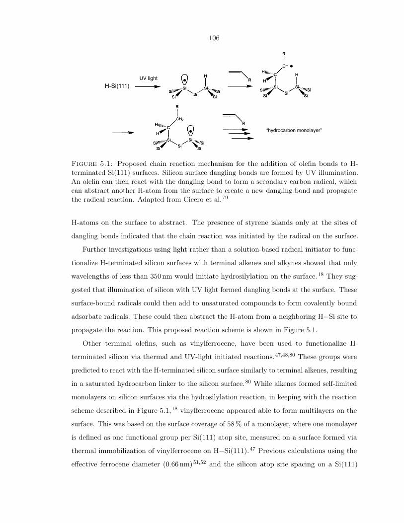
106
H-Si(111)!UV light!
“hydrocarbon monolayer”!
Figure 5.1: Proposed chain reaction mechanism for the addition of olefin bonds to H-terminated Si(111) surfaces. Silicon surface dangling bonds are formed by UV illumination.An olefin can then react with the dangling bond to form a secondary carbon radical, whichcan abstract another H-atom from the surface to create a new dangling bond and propagatethe radical reaction. Adapted from Cicero et al.79
H-atoms on the surface to abstract. The presence of styrene islands only at the sites of
dangling bonds indicated that the chain reaction was initiated by the radical on the surface.
Further investigations using light rather than a solution-based radical initiator to func-
tionalize H-terminated silicon surfaces with terminal alkenes and alkynes showed that only
wavelengths of less than 350 nm would initiate hydrosilylation on the surface.18 They sug-
gested that illumination of silicon with UV light formed dangling bonds at the surface. These
surface-bound radicals could then add to unsaturated compounds to form covalently bound
adsorbate radicals. These could then abstract the H-atom from a neighboring H−Si site to
propagate the reaction. This proposed reaction scheme is shown in Figure 5.1.
Other terminal olefins, such as vinylferrocene, have been used to functionalize H-
terminated silicon via thermal and UV-light initiated reactions.47,48,80 These groups were
predicted to react with the H-terminated silicon surface similarly to terminal alkenes, resulting
in a saturated hydrocarbon linker to the silicon surface.80 While alkenes formed self-limited
monolayers on silicon surfaces via the hydrosilylation reaction, in keeping with the reaction
scheme described in Figure 5.1,18 vinylferrocene appeared able to form multilayers on the
surface. This was based on the surface coverage of 58% of a monolayer, where one monolayer
is defined as one functional group per Si(111) atop site, measured on a surface formed via
thermal immobilization of vinylferrocene on H−Si(111).47 Previous calculations using the
effective ferrocene diameter (0.66 nm)51,52 and the silicon atop site spacing on a Si(111)

107
surface had shown that a closely-packed monolayer of ferrocene would occupy 34% of the atop
sites, and so a surface coverage of >34% of a monolayer indicated multilayer formation of
vinylferrocene.47 Similar results were seen in this work where H-terminated surfaces modified
by vinylferrocene via thermal and UV-light initiated reactions had surface coverages of up to
1 monolayer (see Figure 3.2). This suggested that the hydrosilylation reaction mechanism
was somewhat more complicated for vinyl-appended species like vinylferrocene, possibly
because of polymerization by the vinyl group.
5.1.1 The “Chlorosilylation” Reaction Mechanism
Our development of a new method for mixed monolayer formation hinged on our ability to
perform a hydrosilylation-like reaction wherein a vinyl-appended functional group was reacted
with a Cl-terminated silicon surface. This reaction is hereafter referred to as “chlorosilylation.”
We hypothesized that this reaction occurred through a similar radical mechanism to the
hydrosilylation reaction based on the similarity of the resultant structures for H−Si and
Cl−Si surfaces reacted thermally with vFc. This reaction appeared successful, using both
thermal and UV-light initiated approaches, much like the hydrosilylation reaction.14,17,18
The addition of a radical initiator, benzoyl peroxide, to the reaction solution dramatically
increased the reaction rate, which supported our hypothesis of a radical mechanism for this
reaction.
A similar radical chain reaction mechanism on the Cl−Si surface would require the
abstraction of a neighboring Cl-atom, rather than a H-atom, by the surface-bonded secondary
carbon radical. This would result in the addition of the chlorine to the β-carbon of the newly
attached alkyl chain. There was frequently a chlorine signal by XPS on surfaces modified
by the chlorosilylation reaction, but the Cl 2s peak was too broad to distinguish between
residual Cl−Si and newly-formed Cl−C (see Figure 3.4). In addition, surfaces that were
exposed to methyl Grignard following the chlorosilylation reaction did not generally have a
Cl 2s XPS signal, presumably because any remaining Cl−Si sites would have reacted with
the methyl Grignard. However, it is possible that a chlorine on the β-carbon of the alkyl
group would also be reactive with methyl Grignard. It is also possible that having a chlorine
group on the linker facilitated β-hydride elimination, resulting in a double bond and loss of a
H−Cl group. We saw no evidence for a double bond on the surface, however. Thus we were
unable to definitively characterize the linker between the silicon surface and the ferrocene or
108
bipyridine moiety, making it difficult to determine whether the chain reaction mechanism
was the mechanism for the chlorosilylation reaction occurring on our surfaces.
The decreased efficiency of the UV-light induced reaction on the Cl−Si vs. the H−Si
surfaces also presented a problem if these reactions were proceeding through similar mech-
anisms. The Si−H and Si−Cl bond energies are 70.4 and 85.7 kcalmol−1, respectively, for
non-hindered silanes.81 These energies correspond to light of 406 and 333 nm, respectively,
which are both much lower in energy than the 254 nm UV-light source used in the reaction.
However, previous work using UV-light to initiate hydrosilylation on H-terminated silicon
determined that the reaction did not proceed efficiently if light with wavelengths of ≥350 nm
was used.18 This implies that the energy required to form a dangling bond on the Si−H
surface is actually higher than the non-hindered Si−H bond energy by at least 11.5 kcalmol−1.
There is a 15 kcalmol−1 difference in energy between the H−Si and Cl−Si bond energies,
which corresponds to a difference of ∼70 nm. This energy difference could explain why
illumination with 254 nm light initiates the hydrosilylation reaction, but is much less efficient
for the chlorosilylation reaction. Using a higher-energy, shorter-wavelength UV-light source
could increase the reactivity of the Cl−Si surface. Addition of the radical initiator, benzoyl
peroxide, to the reaction solution alleviated this problem, resulting in efficient reaction of
the Cl−Si surface with vinyl-appended reactants. However, it is unclear whether the radical
initiator is increasing the reaction rate by creating dangling bonds on the surface, or by
creating reactive vinyl radicals in solution.
5.1.2 Addition of 1-Alkenes to Cl−Si(111) Surfaces
Polymerization of the vinyl-appended reagents used to modify our Cl−Si surfaces often
resulted in multilayer formation (see Table 4.1). Limiting the reaction time allowed us to
control the surface coverage of the vinyl-appended moieties on the surface, but the surface
characterization techniques available could not preclude the presence of some polymerized
product on our surfaces. While the mixed methyl/bipyridyl surfaces formed using the
chlorosilylation reaction displayed excellent photoelectrochemical properties, charge transfer
to the attached species often did not proceed readily, and polymerization of the bipyridyl
groups could be one explanation for that. Hydrosilylation of 1-alkenes does not result in
polymerized product on the surface because there is no mechanism for the polymerization
of these species in solution. We therefore decided to extend the chlorosilylation reaction to

109
include 1-alkenes and thus prevent polymerization of the reactant on the surface.
Figure 5.2 shows the high-resolution XPS of H−Si and Cl−Si surfaces reacted with
1-hexene under UV illumination for 1–2 h. Experimental details of this reaction can be found
in Appendix A.15. The Si 2p region of both surfaces have the typical doublet around 99 and
100 eV, with an area ratio of 2:1. The Cl−Si surface had a small Si−O component at 103 eV
that was absent on the H−Si surface. This suggested that the surface coverage of hexene
was higher on the H−Si surface than on the Cl−Si surface. The C 1s region of the H−Si
surface had a large peak at 285 eV, with smaller shoulders at 284, 286, and 287 eV. The
signal at 284 eV was from the surface-bound carbon of the hexene group and corresponded
to 0.28± 0.05 monolayers.13,29 The total carbon coverage on this surface corresponded to
0.8± 0.1 monolayers of hexene, which indicated that there is some non-specific adsorption of
the hexene onto the surface as well, or a large adventitious carbon contribution. The C 1s
region of the Cl−Si surface had a peak at 285 eV, with smaller shoulders at 286 and 287 eV.
There was no C−Si component at 284 eV on this surface, which indicated that there was
little to no covalent attachment of the hexene under these reaction conditions. The total C 1s
signal on this surface corresponded to 0.40± 0.05 monolayers of hexene, which could be from
non-specific adsorption or from adventitious carbon. Both surfaces had a similar amount of
non-covalently bound hexene, which suggested a similar mechanism for nonspecific adsorption
of adventitious carbon. The Cl 2s region of the Cl−Si surface had a large peak at 270 eV,
presumably from residual Cl−Si remaining on the surface, corresponding to 0.45± 0.05
monolayers. It was also possible that this Cl signal was from Cl-atoms that were transferred
to the hexene chain during the radical chain reaction mechanism. However, the peak was
too broad to distinguish multiple components or to detect any significant binding energy
shift in the signal. The H−Si surface had a small chlorine signal at 271 eV, which was likely
from residual solvent because this surface was not chlorinated.
These results indicated that 1-hexene reacted efficiently with the H−Si surface through a
hydrosilylation reaction under UV illumination. The Cl−Si surface did not appear to react
efficiently with 1-hexene under the same reaction conditions based on the absence of a C−Si
peak in the C 1s region, which suggested that the chlorosilylation reaction did not proceed.
However, the large adventitious contributions to the C 1s signal on both surfaces made an
accurate assessment of the surface coverage of hexene complicated.
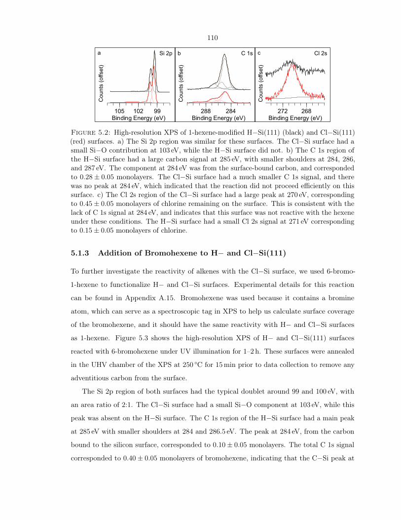
110
Cou
nts
105 102 99Binding Energy (eV)
Cou
nts
288 284Binding Energy (eV)
Cou
nts
272 268Binding Energy (eV)
Cou
nts
(offs
et)
Cou
nts
(offs
et)
Cou
nts
(offs
et)
Si 2p C 1s Cl 2s a b c
Figure 5.2: High-resolution XPS of 1-hexene-modified H−Si(111) (black) and Cl−Si(111)(red) surfaces. a) The Si 2p region was similar for these surfaces. The Cl−Si surface had asmall Si−O contribution at 103 eV, while the H−Si surface did not. b) The C 1s region ofthe H−Si surface had a large carbon signal at 285 eV, with smaller shoulders at 284, 286,and 287 eV. The component at 284 eV was from the surface-bound carbon, and correspondedto 0.28± 0.05 monolayers. The Cl−Si surface had a much smaller C 1s signal, and therewas no peak at 284 eV, which indicated that the reaction did not proceed efficiently on thissurface. c) The Cl 2s region of the Cl−Si surface had a large peak at 270 eV, correspondingto 0.45± 0.05 monolayers of chlorine remaining on the surface. This is consistent with thelack of C 1s signal at 284 eV, and indicates that this surface was not reactive with the hexeneunder these conditions. The H−Si surface had a small Cl 2s signal at 271 eV correspondingto 0.15± 0.05 monolayers of chlorine.
5.1.3 Addition of Bromohexene to H− and Cl−Si(111)
To further investigate the reactivity of alkenes with the Cl−Si surface, we used 6-bromo-
1-hexene to functionalize H− and Cl−Si surfaces. Experimental details for this reaction
can be found in Appendix A.15. Bromohexene was used because it contains a bromine
atom, which can serve as a spectroscopic tag in XPS to help us calculate surface coverage
of the bromohexene, and it should have the same reactivity with H− and Cl−Si surfaces
as 1-hexene. Figure 5.3 shows the high-resolution XPS of H− and Cl−Si(111) surfaces
reacted with 6-bromohexene under UV illumination for 1–2 h. These surfaces were annealed
in the UHV chamber of the XPS at 250 C for 15min prior to data collection to remove any
adventitious carbon from the surface.
The Si 2p region of both surfaces had the typical doublet around 99 and 100 eV, with
an area ratio of 2:1. The Cl−Si surface had a small Si−O component at 103 eV, while this
peak was absent on the H−Si surface. The C 1s region of the H−Si surface had a main peak
at 285 eV with smaller shoulders at 284 and 286.5 eV. The peak at 284 eV, from the carbon
bound to the silicon surface, corresponded to 0.10± 0.05 monolayers. The total C 1s signal
corresponded to 0.40± 0.05 monolayers of bromohexene, indicating that the C−Si peak at
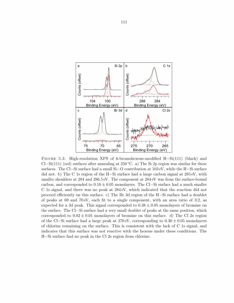
111
Cou
nts
75 70 65Binding Energy (eV)
Cou
nts
104 100Binding Energy (eV)
Cou
nts
288 284Binding Energy (eV)
Cou
nts
275 270 265Binding Energy (eV)
Cou
nts
(offs
et)
Cou
nts
(offs
et)
Cou
nts
(offs
et)
Cou
nts
(offs
et)
Si 2p C 1s a b
Br 3d Cl 2s c d
Figure 5.3: High-resolution XPS of 6-bromohexene-modified H−Si(111) (black) andCl−Si(111) (red) surfaces after annealing at 250 C. a) The Si 2p region was similar for thesesurfaces. The Cl−Si surface had a small Si−O contribution at 103 eV, while the H−Si surfacedid not. b) The C 1s region of the H−Si surface had a large carbon signal at 285 eV, withsmaller shoulders at 284 and 286.5 eV. The component at 284 eV was from the surface-boundcarbon, and corresponded to 0.10± 0.05 monolayers. The Cl−Si surface had a much smallerC 1s signal, and there was no peak at 284 eV, which indicated that the reaction did notproceed efficiently on this surface. c) The Br 3d region of the H−Si surface had a doubletof peaks at 69 and 70 eV, each fit to a single component, with an area ratio of 3:2, asexpected for a 3d peak. This signal corresponded to 0.38± 0.05 monolayers of bromine onthe surface. The Cl−Si surface had a very small doublet of peaks at the same position, whichcorresponded to 0.02± 0.01 monolayers of bromine on this surface. d) The Cl 2s regionof the Cl−Si surface had a large peak at 270 eV, corresponding to 0.30± 0.05 monolayersof chlorine remaining on the surface. This is consistent with the lack of C 1s signal, andindicates that this surface was not reactive with the hexene under these conditions. TheH−Si surface had no peak in the Cl 2s region from chlorine.
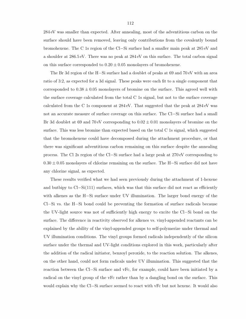
112
284 eV was smaller than expected. After annealing, most of the adventitious carbon on the
surface should have been removed, leaving only contributions from the covalently bound
bromohexene. The C 1s region of the Cl−Si surface had a smaller main peak at 285 eV and
a shoulder at 286.5 eV. There was no peak at 284 eV on this surface. The total carbon signal
on this surface corresponded to 0.20± 0.05 monolayers of bromohexene.
The Br 3d region of the H−Si surface had a doublet of peaks at 69 and 70 eV with an area
ratio of 3:2, as expected for a 3d signal. These peaks were each fit to a single component that
corresponded to 0.38± 0.05 monolayers of bromine on the surface. This agreed well with
the surface coverage calculated from the total C 1s signal, but not to the surface coverage
calculated from the C 1s component at 284 eV. That suggested that the peak at 284 eV was
not an accurate measure of surface coverage on this surface. The Cl−Si surface had a small
Br 3d doublet at 69 and 70 eV corresponding to 0.02± 0.01 monolayers of bromine on the
surface. This was less bromine than expected based on the total C 1s signal, which suggested
that the bromohexene could have decomposed during the attachment procedure, or that
there was significant adventitious carbon remaining on this surface despite the annealing
process. The Cl 2s region of the Cl−Si surface had a large peak at 270 eV corresponding to
0.30± 0.05 monolayers of chlorine remaining on the surface. The H−Si surface did not have
any chlorine signal, as expected.
These results verified what we had seen previously during the attachment of 1-hexene
and butbipy to Cl−Si(111) surfaces, which was that this surface did not react as efficiently
with alkenes as the H−Si surface under UV illumination. The larger bond energy of the
Cl−Si vs. the H−Si bond could be preventing the formation of surface radicals because
the UV-light source was not of sufficiently high energy to excite the Cl−Si bond on the
surface. The difference in reactivity observed for alkenes vs. vinyl-appended reactants can be
explained by the ability of the vinyl-appended groups to self-polymerize under thermal and
UV illumination conditions. The vinyl groups formed radicals independently of the silicon
surface under the thermal and UV-light conditions explored in this work, particularly after
the addition of the radical initiator, benzoyl peroxide, to the reaction solution. The alkenes,
on the other hand, could not form radicals under UV illumination. This suggested that the
reaction between the Cl−Si surface and vFc, for example, could have been initiated by a
radical on the vinyl group of the vFc rather than by a dangling bond on the surface. This
would explain why the Cl−Si surface seemed to react with vFc but not hexene. It would also
113
explain why multilayers formed on H−Si surfaces modified thermally with vinylferrocene,47
for which the chain reaction mechanism is insufficient.79
5.2 Evidence for Surface Attachment
Direct proof of the Si-C bond on surfaces formed via hydrosilylation was generally difficult to
find. Much of the evidence for the covalent attachment of alkenes to silicon surfaces was based
on the robustness of the resultant structures.16,82 Direct proof of covalent attachment was
more straightforward for methyl-terminated silicon formed by the halogenation/alkylation
method, where spectroscopic evidence of the Si-C bond can be obtained.13,29,83 The C 1s
XPS signal at 284 eV, attributed to carbon from the Si−CH3 group, provided strong evidence
for a covalent linkage between the methyl group and the surface. Further studies with other
alkyl chains attached via the halogen/alkylation method also showed this signal at 284 eV,
indicating that these longer chains were attached through a C−Si linkage.32,37 This C−Si
peak at 284 eV was also seen on some alkylated silicon surfaces formed via hydrosilylation of
terminal olefins, providing further evidence of the covalent attachment.18,82
However, surfaces modified by styrene and vinylferrocene via thermal immobilization did
not have this peak at 284 eV in the high-resolution C 1s XPS region.47,84 The absence of
this peak was given as evidence for a saturated hydrocarbon linkage between the ferrocene
group and the silicon surface. This was consistent with results seen in this work on H- and
Cl-terminated surfaces modified by vinylferrocene, vinylbipyridine, and 4-fluorostyrene via
thermal and UV-light initiated reactions. These surfaces did not have peaks at 284 eV in the
high-resolution C 1s XPS region. It was unclear why silicon surfaces terminated by alkyl
groups like methyl, allyl, or octyl would have this peak at 284 eV, ostensibly attributed to
the C−Si carbon, but silicon surfaces terminated by styrene or vinylferrocene, which were
also covalently attached to the surface through a C−Si group, did not.
One possible explanation was that the presence of an electron-withdrawing group, like the
fluorophenyl ring of 4-fluorostyrene or the Cp∗ of vinylferrocene, could shift the binding energy
of the carbon bound to silicon. The electronegativity of Si is less than that of C, and so the
carbon bound to the Si surface was more negatively charged, or reduced, compared to the rest
of the carbons in the alkyl chain, which decreased the binding energy of the surface attached
carbon to 284 eV from 285 eV. On the other hand, when an electron-withdrawing group

114
0
10
20
30
40
282 285 288 Cou
nts
(Tho
usan
ds)
Binding Energy (eV)
0
5
10
684 687 690 693 Cou
nts
(Tho
usan
ds)
Binding Energy (eV)
F 1s a b
C 1s
Figure 5.4: High-resolution F1s and C 1s XPS of silicon surfaces formed by thermal-immobilization of 4-fluorostyrene on Cl−Si(111). a) The F 1s region had a single peak at688 eV from the fluorine group of the 4-fluorostyrene moiety. b) The C 1s region had alarge peak at 286 eV from the carbon atoms of the styrene group. There was also a smallercomponent at 288 eV from the carbon bound to the fluorine. This peak was shifted to higherbinding energy because the fluorine group is more electron-withdrawing than the carbon.Adapted with permission from Lattimer et al.34 Copyright 2013 American Chemical Society.
was bound to carbon, the carbon becomes more positively charged, or oxidized, resulting in
increased binding energy, as for the carbon bound to fluorine seen on 4-fluorostyrene-modified
silicon surfaces (Figure 5.4). The experimental details for the formation of the 4-fluorostyrene-
terminated silicon surface can be found in Appendix A.9. The binding energy of this carbon
was shifted from 286 eV to 288 eV because of the fluorine group. When the surface-bound
carbon is also bound to an electron-withdrawing group, like a hydroxide or fluorine group,
these two effects could be offset, resulting in the absence of the expected C−Si peak at
284 eV. Some evidence for this theory was given by Yaffe et al. in their work on the reaction
between 1-alcohols and H−Si(111).85 They showed that the C 1s region of a surface formed
via the UV-light initiated radical chain reaction between H−Si(111) and 1-decanol had no
peak at 284 eV because the surface-bound carbon had bonds to both the silicon surface and
to the alcohol group. These competing groups had opposite effects on the binding energy of
the surface-bound carbon, resulting in an intermediate shift that was indistinguishable from
the bulk C 1s signal. They performed DFT computations which supported this assertion,
calculating that the C−Si binding energy shift was −1.1 eV, while the C−O binding energy
shift was +1 eV. This agreed well with their experimental results, and with our observations
on methyl-terminated surfaces. Fluorine is even more electronegative than oxygen, and so a
larger shift in the C−F binding energy was not unexpected.
These competing shifts in the binding energy could explain why the C 1s peak at 284 eV
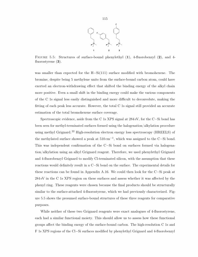
115
Si Si
F
1 2 3
Si
F
Figure 5.5: Structures of surface-bound phenylethyl (1), 4-fluorobenzyl (2), and 4-fluorostyrene (3).
was smaller than expected for the H−Si(111) surface modified with bromohexene. The
bromine, despite being 5 methylene units from the surface-bound carbon atom, could have
exerted an electron-withdrawing effect that shifted the binding energy of the alkyl chain
more positive. Even a small shift in the binding energy could make the various components
of the C 1s signal less easily distinguished and more difficult to deconvolute, making the
fitting of each peak less accurate. However, the total C 1s signal still provided an accurate
estimation of the total bromohexene surface coverage.
Spectroscopic evidence, aside from the C 1s XPS signal at 284 eV, for the C−Si bond has
been seen for methyl-terminated surfaces formed using the halogenation/alkylation procedure
using methyl Grignard.22 High-resolution electron energy loss spectroscopy (HREELS) of
the methylated surface showed a peak at 510 cm−1, which was assigned to the C−Si bond.
This was independent confirmation of the C−Si bond on surfaces formed via halogena-
tion/alkylation using an alkyl Grignard reagent. Therefore, we used phenylethyl Grignard
and 4-fluorobenzyl Grignard to modify Cl-terminated silicon, with the assumption that these
reactions would definitely result in a C−Si bond on the surface. The experimental details for
these reactions can be found in Appendix A.16. We could then look for the C−Si peak at
284 eV in the C 1s XPS region on these surfaces and assess whether it was affected by the
phenyl ring. These reagents were chosen because the final products should be structurally
similar to the surface-attached 4-fluorostyrene, which we had previously characterized. Fig-
ure 5.5 shows the presumed surface-bound structures of these three reagents for comparative
purposes.
While neither of these two Grignard reagents were exact analogues of 4-fluorostyrene,
each had a similar functional moiety. This should allow us to assess how these functional
groups affect the binding energy of the surface-bound carbon. The high-resolution C 1s and
F 1s XPS regions of the Cl−Si surfaces modified by phenylethyl Grignard and 4-fluorobenzyl

116
Cou
nts
288 284Binding Energy (eV)
Cou
nts
692 688 684Binding Energy (eV)
Cou
nts
288 284Binding Energy (eV)
C 1s a C 1s b F 1s c
Figure 5.6: High-resolution C 1s and F 1s XPS of Cl−Si(111) surfaces after reaction with4-fluorobenzyl Grignard (black) and phenylethyl Grignard (red). a) The C 1s region of the4-fluorobenzyl-modified surface was fit to a broad peak at 285 eV and a smaller peak at 287 eV.The peak at 287 eV can be attributed to the carbon bound to the fluorine group, while thebroad peak at 285 eV contains contributions from the benzene ring and the surface-attachedcarbon. There was no distinct C−Si peak at 284 eV in this spectrum. b) The C 1s region ofthe phenylethyl-modified surface was fit to a large peak at 285 eV, with two shoulders at 284and 286 eV. The peak at 284 eV, corresponding to 0.30± 0.05 monolayers, was attributed tothe surface-bound carbon. c) The F 1s region of the 4-fluorobenzyl-modified surface had asingle peak at 687 eV, while the phenylethyl surface had no peak in the F 1s region.
Grignard are shown in Figure 5.6. The C 1s region of the 4-fluorobenzyl-modified surface
appeared similar to the 4-fluorostyrene-modified surface shown in Figure 5.4. There was one
large, broad peak at 285 eV and a smaller peak at 287 eV, which was attributed to the carbon
bound to the fluorine group. This indicated that the fluorine group shifted the C−F binding
energy by about 2 eV, as seen on the 4-fluorostyrene-modified surface. The total carbon signal
corresponded to 0.45± 0.05 monolayers of 4-fluorobenzyl on the surface. The F 1s region of
this surface had a single peak at 687 eV from the fluorine on the surface-bound 4-fluorobenzyl
group, corresponding to 0.34± 0.05 monolayers. This indicated that the 4-fluorobenzyl was
intact on the surface, and that there was some adventitious carbon. The Cl 2s region (not
shown) had a signal corresponding to 0.28± 0.05 monolayers, indicating that there were still
unreacted Cl−Si sites on the surface, which was not unexpected since the surface coverage
of 4-fluorobenzyl was only ∼35% of the Si atop sites.
The C 1s region of the phenylethyl-modified surface was fit to a large peak at 285 eV, with
two shoulders at 284 and 286 eV. The peak at 284 eV, which corresponded to 0.30± 0.05
monolayers, was attributed to the surface-bound carbon of the phenylethyl group.13,29 The
total C 1s signal corresponded to 0.47± 0.05 monolayers, indicating that the phenylethyl
group was intact on the surface and that there was some adventitious carbon. The phenylethyl-
modified surface did not have any signal in the F 1s region, as expected.

117
These results indicated that the presence of the phenylethyl group did not significantly
obscure the C 1s peak at 284 eV from the surface-attached carbon. This suggested that the
phenyl group did not shift the binding energy of that surface-attached carbon. However, the
fluorine group did seem to have some effect, obscuring the C 1s peak at 284 eV on surfaces
modified by both 4-fluorobenzyl and 4-fluorostyrene. This suggested that the fluorine group,
possibly in conjunction with the phenyl ring, exerted some effect on the binding energy of the
surface-bound carbon, shifting it back toward 285 eV from 284 eV. This gave some credence
to the theory proposed by Yaffe et al. about the effects of electron-withdrawing groups on
the binding energy of alkyl groups bound to silicon surfaces, and could explain why we often
do not see a peak at 284 eV on surfaces with covalently-bound carbon groups.85
5.3 Conclusion
Determination of the reaction mechanism for the chlorosilylation reaction developed in this
dissertation was ultimately inconclusive. We began with the hypothesis that the reaction
occurred through a similar mechanism to that proposed for hydrosilylation of terminal alkenes
onto silicon surfaces. We had some evidence for a radical mechanism, based on the increase
in reaction rate observed upon the addition of radical initiators to the reaction solution.
The presence of a chlorine signal in XPS on surfaces modified by chlorosilylation suggested
that the radical chain reaction mechanism observed in hydrosilylation reactions could be
occurring on our surfaces as well. However, the Cl 2s signal was too broad to distinguish
between Cl−Si and Cl−C bonds, making it impossible to tell whether the chlorine on the
surface is from residual, unreacted Cl−Si sites or from chlorine that was abstracted by a
surface-bonded secondary carbon radical. The inability of our Cl−Si surfaces to react with
hexene under UV-illumination suggested that our reaction did not proceed via a UV-light
generated dangling-bond on the surface, unlike the hydrosilylation reaction. Rather, we only
saw reactivity of the Cl−Si bond with vinyl-appended functional groups that were capable
of self-polymerization. This suggested that the chlorosilylation reaction actually proceeded
via a vinyl-radical on the reactant species in solution which could add to the Cl−Si bond on
the surface. However, we currently have only circumstantial evidence that this is the case.
Further experiments, possibly using a shorter-wavelength UV-light source or reacting model
compounds in solution, could help to elucidate the reaction mechanism.
118
Appendix A
Materials and Methods
All chemicals were used as received, unless otherwise specified. Water with a resistivity
≥18.0MΩ · cm was obtained from a Barnstead E-pure system. Electrochemical experiments
were performed using single-side polished, degenerately B-doped p+-Si(111) wafers with
a resistivity of 0.01–0.03Ω · cm. Charge-carrier lifetime measurements were performed
using double-side polished monocrystalline, high-purity As-doped n-type Si(111) wafers
of 350± 25 µm thickness with resistivity of 4–8 kΩ · cm (Topsil, Santa Clara, CA). FTIR
and photoelectrochemical experiments were performed using double-side polished, float-
zone grown, n-type Si(111) wafers (Silicon Quest International, Santa Clara, CA) with
resistivity of 63–77Ω · cm and a thickness of 440± 10mm. Addition photoelectrochemical
experiments were performed using degenerately doped n+-type silicon with resistivity of
0.004–0.006Ω · cm, and n-type silicon with resistivities of 0.019–0.023Ω · cm, 0.8–1.5Ω · cm,
1–10Ω · cm, and 23–34Ω · cm (Silicon Quest International, Santa Clara, CA). All wafers were
modified using techniques described previously and characterized by XPS.13,22,32,34,37,58
A.1 Preparation of H-terminated and Cl-terminated Si(111)
Wafers
Si(111) wafers were cut into ∼1 cm2 pieces which were immersed in boiling piranha solution
(1:2 v/v 10.1M hydrogen peroxide (H2O2, aq):18M sulfuric acid (H2SO4)) for 10min, followed
by rinsing with H2O. The wafers were then etched for 18 s in buffered HF (aq) (NH4F/HF,
Transene) and placed for 15min, without rinsing, in a solution of 40% NH4F (aq) (Transene)
that had been degassed with Ar(g) for at least 30min. The resulting H−Si(111) samples
were rinsed with water and dried under a stream of N2(g). After being transferred to a
119
N2(g)-purged flush box, the H−Si(111) surfaces were placed in a saturated solution of PCl5(98%, Alfa Aesar) in chlorobenzene (99.8%, Sigma-Aldrich) with a few grains of benzoyl
peroxide (reagent grade, 97%, Sigma-Aldrich) added as a radical initiator. After 45–60min
at 90–100 C, the resulting Cl−Si(111) samples were removed from the solution, allowed to
cool, and rinsed with tetrahydrofuran (THF, ≥99.9%, inhibitor free, Sigma-Aldrich).
A.2 Preparation of Methyl-Terminated Si(111) Surfaces
CH3−Si(111) surfaces were produced in a N2-purged flush box by immersing Cl−Si(111)
surfaces in 1.0M CH3MgCl (diluted with THF from 3.0M CH3MgCl, Sigma-Aldrich) at
65 C for 2–3 h. To remove and quench any unreacted Grignard reagent, the samples were
rinsed with THF, then rinsed with CH3OH (Sigma-Aldrich, 99.8%), and removed from the
flush box. All subsequent Grignard-modified surfaces were also cleaned in this manner before
removal from the flush box. H−Si(111) surfaces were also reacted in the same manner with
methyl Grignard as a control. After removal from the flush box, all surfaces were subjected
to sonication sequentially in THF, CH3OH, and water for 10min each to clean the surfaces
prior to characterization by surface-sensitive spectroscopy.
A.3 Preparation of Allyl- and Mixed Methyl/Allyl-Termin-
ated Si(111) Surfaces
Allyl-Si(111) surfaces were produced in a N2-purged flush box by immersing Cl−Si(111)
surfaces in 1.0M C3H5MgCl (diluted with THF from 2.0M C3H5MgCl, Sigma-Aldrich) at
65 C for 2–3 h. Mixed methyl/allyl-terminated surfaces were produced by forming solutions
of 1.0M Grignard with varying ratios of methyl:allyl components. For example, the 10% allyl
solution was produced by combining 0.25mL 2.0M C3H5MgCl, 1.5mL 3.0M CH3MgCl, and
3.25mL THF to form 5mL of the 10% allyl solution. Cl−Si(111) surfaces were then immersed
in this solution at 65 C for 2–3 h to produce the mixed surface. After functionalization with
the Grignard solution, the surfaces were rinsed, removed from the flush box, and cleaned as
described above.
120
A.4 Bromination of Functionalized Si(111) Surfaces
Bromination reactions were all carried out in a N2-purged flush box. Surfaces were brominated
by immersion in a 5% Br2 solution in CH3OH. This solution was formed by dilution of
0.5mL Br2 (Sigma-Aldrich) with CH3OH to a final volume of 10mL. All reactions were
carried out at RT. Immersion time was varied between 2 and 60min, depending on the
desired product. Surfaces were rinsed with CH3OH before removal from the flush box, and
then sonicated sequentially in CH3OH and water for 10min each prior to characterization.
A.5 Preparation of Butenyl- and Mixed Methyl/Butenyl-Ter-
minated Si(111) Surfaces
Butenyl−Si(111) surfaces were produced by immersing Cl−Si(111) surfaces in a N2-purged
flush box in 0.5M C4H7MgBr (Sigma-Aldrich) at 65 C for 2–3 h. Mixed methyl/butenyl-
terminated surfaces were produced in a one-step synthesis by forming solutions of 1.0M
Grignard with varying ratios of methyl:butenyl components. For example, the 15% butenyl
solution was produced by combining 1.5mL 0.5M C4H7MgBr, 1.4mL 3.0M CH3MgCl,
and 2.1mL THF to form 5mL of the 15% butenyl solution. Cl−Si(111) surfaces were
then immersed in this solution at 65 C for 2–3 h to produce the mixed surface. Partial
butenyl-terminated surfaces were produced by decreasing the reaction temperature to room
temperature (r.t.) and decreasing the time in which the Cl−Si(111) surface was immersed in
the 0.5M C4H7MgBr solution to between 5 and 90min. Mixed methyl/butenyl-terminated
surfaces were produced in a two-step synthesis by first immersing Cl−Si(111) surfaces in
0.5M C4H7MgBr at r.t. for a predetermined period of time between 5 and 90min, followed
by immersion in 1.0M CH3MgCl at 65 C for 1–2 h. After functionalization all surfaces were
rinsed, removed from the flush box, and cleaned by sonication as described above.
A.6 Cross-Coupling Reactions with 4-VinylPhenyl Acetamide,
4-VinylPhenyl Isocyanide, and Vinylferrocene
Cross-coupling reactions with the mixed butenyl/methyl surfaces were performed in a two-step
process. All reaction steps were carried out under an Ar atmosphere in a dry glove box. First,

121
the mixed surface was immersed in 1.0M Grubbs’ catalyst, 2nd generation (Sigma-Aldrich) in
CH2Cl2 in a 15mL glass pressure vessel (Chemglass) with a Teflon screw-cap. The vessel was
held at 50 C in an oil bath for 6–10 h. After cooling, the surface was rinsed with CH2Cl2 and
immersed in 1.0M 4-vinylphenyl acetamide (4-VPA, synthesized by M. Rose), 4-vinylphenyl
isocyanide (4-VPI, synthesized by M. Rose), or vinylferrocene (vFc, Alfa Aesar) in CH2Cl2 in
a fresh 15mL glass pressure vessel. This vessel was held at 50 C in an oil bath for 12–18 h.
After cooling, the surface was rinsed with CH2Cl2 and removed from the dry box. The
surface was then sonicated sequentially in CH2Cl2, CH3OH, and water for 10min each prior
to characterization.
A.7 Metallation of 4-VinylPhenyl Isocyanide with Codmg
The mixed butenyl/methyl surface with cross-coupled 4-VPI was placed in a solution of
10mg Co(dimethylglyoxime)2(BF2)2 (Codmg, synthesized by M. Rose) in 8mL CH3CN at
r.t. for 2.5 h. The surface was then rinsed with CH3CN to remove unreacted Codmg prior to
characterization.
A.8 Thermally-Induced Formation of Vinylferrocenyl-Termin-
ated Si(111) Surfaces
Vinylferrocene-terminated Si surfaces were produced in a N2-purged flush box by immersing
H− and Cl−Si(111) surfaces in neat vFc for 2–3 h at 140 C in pressure vessels. As a separate
control reaction, the H−Si(111) and Cl−Si(111) surfaces were also exposed to ferrocene
(Fc, Sigma-Aldrich) for 2–3 h at 140 C in a N2(g)-purged glove box. Samples with a range
of surficial vFc coverage were prepared from Cl−Si(111) surfaces by lowering the reaction
temperature to 100 C and by decreasing the immersion time in vFc to between 10min and
1 h. To form mixed monolayers, these partially vFc-functionalized Si(111) samples were
then rinsed with THF and placed in 1.0M CH3MgCl in THF at 65 C for 2 h. As a control
reaction, CH3−Si(111) surfaces were immersed in vFc for 2–3 h at 140 C in a N2(g)-purged
glove box. After functionalization, all these surfaces were rinsed with THF and CH3OH, and
removed from the flush box. All functionalized surfaces were then sonicated sequentially in
THF, CH3OH, and H2O for at least 10min each, prior to characterization by surface-sensitive

122
spectroscopy.
A.9 Preparation of 4-Fluorostyrene-Modified Surfaces
In a N2-purged flush box, Cl−Si(111) wafers were immersed in neat 4-fluorostyrene (Aldrich,
99%, with tert-butylcatechol as an inhibitor) at 100 C for 3 h. Mixed 4-fluorostyrene/methyl
surfaces were prepared by immersion of Cl−Si(111) surfaces in neat 4-fluorostyrene at 100 C
for 5min. The samples were then rinsed with THF and immersed in 1.0M CH3MgCl in THF
at 65 C for 3 h. The resulting surfaces were rinsed with THF and CH3OH, removed from
the glove box, and then sonicated sequentially in THF, CH3OH, and H2O for at least 10min
each prior to surface characterization.
A.10 UV-light Induced Formation of Vinylferrocenyl-Termin-
ated Si(111) Surfaces
In a N2-purged flush box, H− and Cl−Si surfaces were placed polished-side down in a solution
of ∼50–100mg vinylferrocene in ∼3mL THF in a glass dish with a quartz bottom. The
wafers were illuminated from below with UV light (254 nm, 18.4W, Mineralight, Upland,
CA) for 1 h. The dish was covered with aluminum foil to minimize solvent evaporation.
After functionalization the wafers were rinsed with THF. Mixed monolayers were formed by
placing the vFc-modified wafer in 1M CH3MgCl in THF at 65 C. This procedure was later
modified by changing the solvent to dichloromethane (CH2Cl2, Sigma-Aldrich, anhydrous)
or acetonitrile (CH3CN, Sigma-Aldrich, anhydrous), adding a few grains of benzoyl peroxide
(Aldrich reagent grade, 97%, Sigma-Aldrich) as a radical initiator, decreasing the amount
of vFc used in solution to ∼10mg, and decreasing the illumination time to between 30 and
180min to control surface coverage. After functionalization, all wafers were rinsed with THF
and CH3OH, then removed from the flush box and sonicated sequentially for 10min each in
THF, CH3OH, and water prior to characterization.
123
A.11 Formation of Mixed Vinylbipyridyl/Methyl Surfaces
In a N2-purged flush box, H− and Cl−Si surfaces were immersed polished-side down in a
solution of ∼10–20mg vinylbipyridine (vbpy, synthesized by W. Sattler) in ∼3mL CH3CN
with a few grains of BP in a glass dish with a quartz bottom, and exposed to UV light
(254 nm, 18.4W, Mineralight, Upland, CA) from below for 0.5 to 3 h. The dish was covered
with aluminum foil to minimize solvent evaporation, with extra solvent added to the reaction
solution as needed to maintain volume. The surfaces were then rinsed with CH3CN and
placed in 1M CH3MgCl in THF at 65 C. The wafers were then rinsed with THF and
CH3OH and removed from the flush box, then cleaned by sonication as described above.
A.12 Attachment of [Cp∗Rh(vbpy)CH3CN](PF6)2
In a N2-purged flush box, Cl−Si surfaces were immersed polished-side down in a solution of
∼10–20mg [Cp∗Rh(vbpy)CH3CN](PF6)2 (synthesized by J. Blakemore) in ∼3mL CH3CN
with a few grains of BP in a glass dish with a quartz bottom, and exposed to UV light
(254 nm, 18.4W, Mineralight, Upland, CA) from below for 2 h. The dish was covered with
aluminum foil to minimize solvent evaporation. The surfaces were then rinsed with CH3CN
and CH3OH and removed from the flush box, then cleaned by sequential sonication for
10min each in CH3CN, CH3OH, and water.
A.13 Formation of Mixed Methyl/Vinylbipyridyl Surfaces
In a N2-purged flush box, H− and Cl−Si surfaces were immersed in a solution of 1M
CH3MgCl in THF at r.t. for 5min. These partially methylated surfaces were rinsed with
THF and then immersed in a solution of ∼10–20mg vinylbipyridine (vbpy, synthesized by
W. Sattler) in ∼3mL CH2Cl2 with a few grains of BP in a glass dish with a quartz bottom,
and exposed to UV light (254 nm, 18.4W, Mineralight, Upland, CA) from below for 1 to 2 h.
The dish was covered with aluminum foil to minimize solvent evaporation, with extra solvent
added as necessary to maintain the solution volume. The surfaces were then rinsed with
CH2Cl2 and CH3OH and removed from the flush box, then cleaned by sequential sonication
for 10min each in CH2Cl2, CH3OH, and water.

124
A.14 Reaction of Butbipy with H− and Cl−Si(111) Surfaces
In a N2-purged flush box, H- and Cl-terminated silicon wafers were placed polished-side
down in a glass dish with a quartz bottom filled with a solution of 10mg 4-(3-Butenyl),4′-
methyl-2,2′-bipyridine (butbipy, synthesized by M. Radlauer) in ∼3mL CH2Cl2 with trace
BP added as a radical initiator. This vessel was illuminated with UV light (254 nm, 18.4W,
Mineralight, Upland, CA) from below for 1 h. The dish was covered with aluminum foil to
minimize solvent evaporation. The surfaces were then removed from the dish and rinsed
with CH2Cl2 and CH3OH, and removed from the flush box. Mixed methyl/butbipy surfaces
were formed by placing a Cl-terminated silicon surface in 1.0M CH3MgCl in THF at r.t. for
5min. The wafer was then rinsed with THF and placed in a glass dish with a quartz bottom
filled with a solution of 10mg butbipy in CH2Cl2 with trace BP added as a radical initiator.
This dish was illuminated with UV light (254 nm, 18.4W, Mineralight, Upland, CA) from
below for 1 h, and covered with aluminum foil to minimize solvent evaporation. The surface
was then removed from the dish, rinsed with CH2Cl2 and CH3OH, and removed from the
flush box. All surfaces modified with butbipy were cleaned by sonication as described above
prior to surface characterization.
A.15 Reaction of Hexene with H− and Cl−Si(111) Surfaces
In a N2-purged flush box, H- and Cl-terminated silicon wafers were placed in an empty glass
dish with a quartz bottom. Three drops of neat 1-hexene (≥99%, Sigma-Aldrich) were placed
on top of each of the wafers, ensuring an even coating of the hexene over the entire surface.
The wafers were then illuminated with UV light (254 nm, 18.4W, Mineralight, Upland, CA)
from above for 1–2 h. The wafers were then removed from the vessel and rinsed with CH2Cl2and CH3OH to remove excess reactant, and removed from the flush box. H− and Cl−Si(111)
surfaces were reacted independently with 1-hexene to prevent cross-contamination of any
reactant between the wafers. 6-Bromo-1-hexene (95%, Sigma-Aldrich) was also reacted with
H− and Cl−Si(111) surfaces following this same procedure. All surfaces were sonicated
sequentially for 10min each in THF, CH3OH, and water prior to characterization.

125
A.16 Formation of Phenylethyl- and 4-Fluorobenzyl-Modified
Surfaces
In a N2-purged flush box, phenylethyl-modified surfaces were prepared by immersing a
Cl−Si(111) surface in a solution of 1.0M phenylethylmagnesium chloride (C6H5CH2CH2MgCl,
1.0M, Sigma-Aldrich) in THF at 65 C for 3 h. The surface was then rinsed with THF and
CH3OH, then removed from the flush box. 4-Fluorobenzyl-modified surfaces were prepared
in a similar manner, by placing a Cl-terminated silicon wafer in a solution of 0.25M 4-
fluorobenzylmagnesium chloride (FC6H4CH2MgCl, 0.25M, Sigma-Aldrich) in THF at 65 C
for 3 h. The surface was then rinsed with THF and CH3OH and removed from the flush box.
All surfaces were cleaned by sonication as described above prior to surface characterization.

126
Appendix B
Instrumentation
B.1 X-ray Photoelectron Spectroscopy
Two X-ray photoelectron spectrometers were used to collect data for this work. The first is
a Surface Science Instruments M-Probe system that has been described previously.24 The
sample chamber was kept at <5× 10⁻⁹ torr and ejected electrons were collected at an angle
of 55° from the surface normal. Survey scans were performed to identify the elements on
the surface of the silicon. Additionally, high-resolution spectra were collected for the Si 2p,
C 1s, Fe 2p, Cl 2s, Br 3d, N 1s, F 1s, Co 2p, and Rh 3d XPS regions. The XPS data were
analyzed using the Hawk Data Analysis Application (V7.03.04; Service Physics, Bend, OR).
The remainder of the X-ray photoelectron spectroscopy (XPS) data were collected using
a Kratos AXIS Ultra system, described previously.62 The pressure in the sample chamber
was kept at <5× 10⁻⁹ torr, and ejected electrons were collected at an angle of 90° from the
surface normal. Survey scans were performed to identify the elements on the surface of
the silicon. Additionally, high-resolution spectra were collected for the Si 2p, C 1s, Fe 2p,
Cl 2s, N 1s, Rh 3d, Ir 4f, Ru 3p, and Br 3d regions. The XPS data were analyzed using
the program Computer Aided Surface Analysis for X-ray Photoelectron Spectroscopy, or
CasaXPS. All XPS signals reported herein are binding energies and are reported in eV. For
spectra that exhibited multiple XPS peaks arising from a single element, the peak was fit to
multiple Voigt functions (80% Gaussian and 20% Lorentzian) when possible to quantitate
the amount of each detectable species for that specific element.

127
B.1.1 Surface Coverage Quantification
The surface coverages of carbon, iron, chlorine, bromine, nitrogen, fluorine, cobalt, rhodium,
iridium, ruthenium, and silicon oxide were calculated as described previously.32 To account
for any variation in the focus or power of the X-ray beam, the Si 2p bulk peak at 99–100 eV
was used to normalize the XPS signals during quantification of surface coverages. Spectra
were not used for quantification if the Si 2p signal showed any significant change in intensity
due to organic overlayers. Hence, an elemental peak, when corrected by its relative sensitivity
factor (RSF), which is a unique value for each elemental peak for each instrument, was
normalized by the observed area of the Si 2p peak. When using the M-probe data for
quantification, the RSF of the C 1s signal is defined as 1.0, while for the Kratos data the
RSF of the F 1s signal is defined as 1.0.
The CH3−Si(111) surface was used as a reference to provide a standard signal area
ratio, θMe, that corresponded to a complete monolayer wherein every Si atop site had been
functionalized by a CH3 group. Accordingly, on CH3−Si(111) surfaces, the area of the C 1s
peak at 284 eV, ascribable to carbon directly attached to silicon, was normalized by the area
of the Si 2p peak, and this ratio was used to determine the value of θMe.25
To calculate the fraction of a monolayer of Si−CH3 groups, ηSi−CH3, that were present on
the mixed-monolayer surfaces, the ratio of the area of the lowest-energy C 1s peak (at 284 eV)
to the Si 2p peak area on that surface was divided by the value of θMe, or ηSi−CH3= θSi−CH3
/θMe.
The total amount of C on a given surface was estimated by using the entire C 1s peak (i.e.,
adding the areas of all the C 1s components) normalized by the area of the Si 2p signal.
A ratio of at least 12:1 C:Fe on the surface (10 carbons from the Cp groups, and 2 from
the vinyl linker) was taken as confirmation of intact Fc groups on the surface for surfaces
modified by vFc.
The amount of Fe on Si(111) surfaces, θFe, was calculated by dividing the area of the Fe
2p3/2 peak at 708 eV, which corresponds to the Fe(II) signal,86 by the relative sensitivity
factor (RSF) of Fe and then by the area of the Si 2p signal on such surfaces. The ratio of θFe
to θMe gave the ratio of the number of Fe(II) atoms on the surface to the number of Si(111)
atop sites, ηFe, i.e., the fraction of the surface sites that were functionalized by vFc. A similar
calculation was performed using the Fe 2p1/2 peak at 721 eV. The two methods in general
gave values for the surface coverage of Fe that were within experimental error of each other.
128
The surface coverage of chlorine was calculated using the Cl 2s peak at 270 eV to calculate
θCl, by taking the area of the Cl 2s peak, dividing by its RSF, and normalizing that area
to the area of the Si 2p signal on that surface. The ratio of θCl to θMe gave the surface
coverage of chlorine as a fraction of Si atop sites, ηCl. The fluorine coverage was quantified
by taking the area of the F 1s peak at ∼688 eV, dividing by its RSF, and normalizing to
the area of its Si 2p peak. This process yielded a value for θF, which was then divided
by θMe to calculate the number of F atoms per Si atop site, ηF. For surfaces modified
by 4-fluorostyrene or 4-fluorobenzyl Grignard, this number was taken to equal the surface
coverage of 4-fluorostyrene or 4-fluorobenzyl. For surfaces modified by Codmg, that number
was divided by 4 to give the total coverage of Codmg on the surface, as there were 4 F
atoms per Codmg unit. For surfaces modified by [Cp∗Rh(vbpy)CH3CN]PF6, that number
was divided by 6 to give the total coverage of [Cp∗Rh(vbpy)CH3CN]PF6 on the surface.
The surface coverage of bromine was calculated using the Br 3d doublet at 69 and 70 eV
to calculated θBr, by taking the area of the Br 3d peak, dividing by its RSF, and normalizing
that area to the area of the Si 2p signal on that surface. The ratio of θBr to θMe gave the
surface coverage of bromine as a fraction of Si atop sites, ηBr. For surfaces with multiple
contributions in the Br 3d region, each set of doublets was analyzed separately to calculate
ηBr for each type of bromine.
The surface coverage of nitrogen was calculated using the N 1s peak at ∼400 eV to
calculate θN, by taking the area of the N 1s peak, dividing by its RSF, and normalizing that
area to the area of the Si 2p signal on that surface. The ratio of θN to θMe gave the surface
coverage of chlorine as a fraction of Si atop sites, ηN. On surfaces modified by 4-VPA or
4-VPI, ηN was taken as the coverage of the group on the surface. For surfaces modified by
Codmg, ηN was divided by 5 to get the coverage of Codmg on the surface]. For surfaces
modified by bipy or butbipy, ηN was divided by 2 to give the total bipy coverage, as there
were 2 N atoms per bpy unit. For surfaces with multiple contributions in the N 1s region,
each component was analyzed separately to calculate ηN for each component.
The surface coverage of cobalt was calculated using the Co 2p doublet at 782 and 797 eV
to calculate θCo, by taking the area of the Co 2p peak, dividing by its RSF, and normalizing
that area to the area of the Si 2p signal on that surface. The ratio of θCo to θMe gave the
surface coverage of chlorine as a fraction of Si atop sites, ηCo. For surfaces modified by
Codmg, ηCo is taken as the total coverage of the Codmg group on the surface.

129
The coverage of rhodium was calculated using the Rh 3d doublet at 310 and 315 eV, which
corresponded to Rh(III), to calculate θRh by taking the area of the Rh 3d peak, dividing
by its RSF, and normalizing that area to the area of the Si 2p signal on that surface. The
ratio of θRh to θMe gave the ratio of the number of Rh(III) atoms on the surface to Si(111)
atop sites, ηRh, which was taken as the surface coverage of any of the Rh(III) complexes,
which each contain one rhodium. A similar calculation was performed using the Rh(I) signal
at 308 and 313 eV to calculate the surface coverage of any Rh(I) formed by reduction or
decomposition of the Rh(III) complexes used in this work. The coverage of iridium was
calculated similarly using the Ir 4f peak at 64 and 65 eV, which corresponded to Ir(III), to
find ηIr. This was taken as the surface coverage of the Cp∗Ir complex, which contained one
iridium. The Ru 3p peaks at 463 and 485 eV, which corresponded to Ru(III), were similarly
used to calculate ruthenium coverage, ηRu. This was taken as the surface coverage of the
Ru(acac)2 complex, which contained one ruthenium.
The amount of silicon oxide on the surface was calculated by taking the area of the broad
Si 2p peak at 101–105 eV (corresponding to oxidized silicon),13 dividing by its RSF, and
normalizing to the area of the bulk Si 2p peak at 99–100 eV, to give θSi−O. This value was
then divided by θMe to give the surface coverage of silicon oxide as a fraction of Si atop sites,
ηSi−O.
B.2 Fourier-Transform Infrared Spectroscopy
Transmission infrared spectroscopy (FTIR) measurements were collected using a Thermo
Scientific Nicolet 6700 Optical Spectrometer that was equipped with a deuterated triglycine
sulfate (DTGS) detector and a purified air purge, described previously.32 FTIR spectra were
collected by mounting the samples at a fixed 74° angle, as measured between the incident
light and the surface normal. The sample chamber was purged with N2 for at least 1 h
before collection of spectra. All of the FTIR spectra represent averages of greater than 2000
consecutive scans. Double-side polished, n-type Si(111) wafers with resistivity of 63–77Ω · cm
and a thickness of 440± 10µm were used for all FTIR measurements. Samples were cut into
1 cm× 3 cm pieces and mounted horizontally. Wafers were prepared for FTIR by rinsing
with water and drying under a stream of N2.

130
B.3 Surface Recombination Velocity
Surface recombination velocity (S) measurements were made using a contactless microwave
conductivity apparatus.30,37 A 20-ns pulsed-diode laser with a wavelength of 905 nm (OSRAM
laser diode with an ETX-10A-93 driver) was used to generate electron-hole pairs in high-
purity, nearly intrinsically As-doped n-Si(111) wafers with resistivity of 4–8 kΩ · cm, with
both sides of the wafer polished and processed equivalently at all stages. The lifetime of the
photogenerated charge carriers was monitored using a PIN diode that detected the microwave
radiation reflected from the sample. Functionalized surfaces that had been prepared using
nearly intrinsically doped Si(111) wafers were tested immediately after preparation, and for
several days or weeks afterward. Between measurements, the samples were stored in the
dark, in air.
Charge-carrier lifetimes were measured by fitting the excess charge-carrier density, A =
∆n + ∆p, where ∆n and ∆p are the photogenerated electron and hole concentrations,
respectively, to a single-exponential decay:
A = y0 + ae−t/τ . (B.1)
The extracted lifetime, τ , was converted to a surface recombination velocity, S, using:
1
τ=
1
τB+
2S
d, (B.2)
where τ and τB are the measured and bulk lifetimes, respectively, and d is the wafer
thickness.32 For high-purity Si, the bulk-carrier lifetime is much larger than the measured τ
(τ−1B τ−1) which allowed the simplification:
S =d
2τ. (B.3)
B.4 Electrochemistry
Nonaqueous electrochemistry of vinylferrocene-modified surfaces was performed in an argon-
filled glove box with acetonitrile (CH3CN, JT Baker, 99.8%) as the solvent and 0.10M
tetraethylammonium perchlorate ((NEt4)ClO4, Alfa Aesar, 98% dry wt, 10% water) as
131
the supporting electrolyte. Prior to use, the (NEt4)ClO4 was recrystallized from CH3OH
and diethyl ether, and was stored under Ar(g). All measurements were made in a three-
electrode cell connected to a Gamry Instruments Reference 600 potentiostat controlled by
Gamry Instruments Framework v.5.61 (2010) software. The counterelectrode was a Pt
mesh and the reference electrode was Ag/AgNO3 (Ag wire immersed in 0.01M AgNO3 in
electrolyte), separated from the solution by a porous Teflon tip (CH Instruments). Ohmic
contact to the p+-Si(111), n+-Si(111), and n-Si(111) samples, for electrochemistry and
photoelectrochemistry, was made by scratching the back of the functionalized wafer with a
Ga-In eutectic and placing the wafer on Cu foil on a stainless steel base. The wafers were
then secured in a custom-made Teflon cell with an O-ring seal used to define the electrode
area (0.28 cm2), as described previously.34 A methyl-terminated Si(111) surface was used
to confirm the absence of redox activity on the surface and in the electrolyte between −1V
and +0.4V vs. Ag/AgNO3. Photoelectrochemistry experiments were performed using an
ELH-type W-halogen bulb with a dichroic rear reflector, adjusted to produce an effective
light intensity of ∼250mW · cm−2 at the electrode surface. The light and dark scans were
alternated to minimize heating of the materials by the lamp.
Electrochemistry of bipy-modified surfaces was performed in a nitrogen-filled glove
box using alumina-dried acetonitrile as the solvent and 0.10M tetrabutylammonium hex-
afluorophosphate ((NBu4)PF6, Fluka electrochemical grade) as the supporting electrolyte.
Measurements were made using a three-electrode configuration and a Princeton Applied
Research Parstat 4000 potentiostat controlled by Princeton Applied Research VersaStudio
v.2.2 (2012) software. The counter electrode was basal plane graphite (BPG) and the
reference electrode was Ag/Ag+ (silver wire immersed in electrolyte, separated from the
solution by a porous Vycor tip (Bioanalytical Systems, Inc.)). Ferrocene (99%, Alfa Aesar)
was added to the electrolyte solution at the conclusion of each experiment ([Fc] ∼1mM);
the ferrocene/ferrocenium couple served as an internal standard for comparing potentials.
Voltammetry on the functionalized surfaces was carried out by first scanning cathodically to
sufficiently reducing potentials to examine redox events for the immobilized metal complexes.
Generally, the sweep width was from 0 to −1.5V vs. Fc/Fc+ at a scan rate of 100mV s−1.
Ohmic contact to the Si wafers was made as described above. Electrochemistry was performed
in the Teflon cell described above.
132
B.4.1 Surface Coverage Quantification
A linear fit was used to subtract the background current from the voltammetric scans
to remove capacitive current from our calculations. The anodic and cathodic waves were
integrated independently to estimate the surface coverage of the electroactive groups. The area
under the background-subtracted current-versus-time plot gave the total charge transferred
to the redox couple, which was then divided by the projected electrode area (0.28 cm2) to
yield the number of electroactive groups per cm2. The integrated areas of the anodic and
cathodic peaks, respectively, were generally within 10% of each other. Multiple scan rates
were used to ensure the reproducibility of the data. For vFc-modified surfaces, the total
number of electrochemically active Fc groups per cm2 divided by the surface density of
silicon atop atoms on a Si(111) surface, 7.8× 10¹⁴ atoms per cm2,25 yielded the fraction of
the Si atop sites covered by electroactive Fc groups, ηFc. 1.0 monolayers of coverage in this
case refers to a situation in which the electrochemically detected coverage corresponded to
7.8× 10¹⁴ electroactive Fc groups per cm2 of projected electrode area. Similar calculations
were performed for bipy-modified surfaces metallated with rhodium and ruthenium complexes
to get the electroactive surface coverage of the Rh or Ru complexes.
B.4.2 Electron Transfer Rate Calculation
Potential-step chronoamperometry was used to measure the electron transfer rate on Si
surfaces modified with vFc. In these experiments, the potential was held at a potential below
the ferrocene redox couple for 3 s, then stepped to a potential above the redox couple and
held for 5 s, then stepped back to a potential below the redox couple. The current follows a
simple exponential decay:
i(t) = kQ exp(−kt), (B.4)
where i is the current in amps as a function of time, k is the charge transfer rate in s−1, and
Q = nFAηFc, where n is the number of electrons in the reaction (one for the Fc/Fc+ couple),
F is Faraday’s constant, A is the area of the electrode, and ηFc is the surface coverage of
electroactive centers. A plot of log(i) vs. t will be linear for the portion of the transient after
double-layer charging, with a slope of −k and an intercept of log(kQ). Because n, F , and A
are all known, and ηFc can be calculated as described in Appendix B.4.1, k can be found for
both the oxidation and reduction of the surface-attached ferrocene redox couple in the dark

133
and in the light.
B.4.3 Aqueous Electrochemistry
Aqueous electrochemistry of vFc-modified surfaces was carried out under ambient conditions
using 1.0M potassium phosphate dibasic (KH2PO4, 99.95%, Sigma-Aldrich) in 18MΩ · cm
water, at pH 4.2, as the electrolyte. Measurements were made using a three-electrode
configuration and a Princeton Applied Research Parstat 4000 potentiostat controlled by
Princeton Applied Research VersaStudio v.2.2 (2012) software. The counter electrode was a
platinum wire and the reference electrode was Ag/Ag+ (silver wire immersed in saturated KCl
(≥99.0%, Sigma-Aldrich), separated from the solution by a porous Vycor tip (Bioanalytical
Systems, Inc.)). The reference electrode was stored in 3.0M NaCl when not in use and had a
potential of 0.197V vs. NHE. Potassium ferricyanide ((K3Fe(CN)6, 99.98%, Sigma-Aldrich)
was added to the electrolyte solution at the conclusion of each experiment to serve as an
internal standard for comparing potentials. Ohmic contact to the Si wafers was made as
described above, and electrochemistry was performed in the Teflon cell described above
(Appendix B.4).
B.5 X-ray Absorption Spectroscopy (XAS) Data Collection
Ir LIII XAS measurements were performed at the Stanford Synchrotron Radiation Laboratory
(SSRL) on Beamline 7-3 at an electron energy of 3.0GeV and an average current of 500mA.
The intensity of the incident X-ray beam was monitored using a N2-filled ion chamber (I0)
in front of the sample. A Si(220) double-crystal monochromator was used to detune to 50%
of the maximum flux to attenuate higher harmonics. The data was collected as fluorescence
excitation spectra with a Ge 30-element detector (Canberra). The monochromator energy
was calibrated using Ir foil (a rising edge energy of 11 215.00 eV).
The powder sample was diluted with boron nitride (1% w/w). The mixture was packed
into 0.5mm thick aluminum sample holders and sealed with Mylar tape. To ensure that no
X-ray induced radiation damage occurred, the LIII edge position was closely monitored for
any reduction.
Data reduction of the XANES spectra was performed using SamView (SixPACK software,
Dr. Samuel M. Webb, SSRL). The pre-edge and post-edge backgrounds were subtracted

134
from the XAS spectra using Athena (IFEFFIT software), and the resulting spectra were
normalized with respect to the edge height.

135
References
[1] Ibrahim, H.; Ilinca, A.; Perron, J. Energy storage systems—Characteristics and compar-isons. Renew. Sust. Energ. Rev. 2008, 12, 1221–1250.
[2] Gray, H. B. Powering the planet with solar fuel. Nat. Chem. 2009, 1, 7–7.
[3] Tran, P. D.; Barber, J. Proton reduction to hydrogen in biological and chemical systems.Phys. Chem. Chem. Phys. 2012, 14, 13772–13784.
[4] Santori, E. A. Si microwire array photoanodes for artificial photosynthetic devices. Ph.D.thesis, California Institute of Technology, 2013.
[5] Tan, M. X.; Laibinis, P. E.; Nguyen, S. T.; Kesselman, J. M.; Stanton, C. E.; Lewis, N. S.Principles and Applications of Semiconductor Photoelectrochemistry. Prog. Inorg. Chem.1994, 41, 21–144.
[6] Streetman, B. G.; Banerjee, S. Solid state electronic devices; Prentice Hall: UpperSaddle River, N.J., 2000.
[7] Grimes, C. A.; Varghese, O. K.; Ranjan, S. Light, water, hydrogen; The Solar Generationof Hydrogen by Water Photoelectrolysis; Springer: New York, NY, 2008.
[8] DeBenedetti, W.; Chabal, Y. J. Functionalization of oxide-free silicon surfaces. J. Vac.Sci. Technol. A 2013,
[9] Pike, A. R.; Lie, L. H.; Eagling, R. A.; Ryder, L. C.; Patole, S. N.; Connolly, B. A.;Horrocks, B. R.; Houlton, A. DNA On Silicon Devices: On-Chip Synthesis, Hybridization,and Charge Transfer. Angew. Chem. Int. Ed. 2002, 41, 615–617.
[10] Strother, T.; Cai, W.; Zhao, X. S.; Hamers, R. J.; Smith, L. M. Synthesis and char-acterization of DNA-modified silicon (111) surfaces. J. Am. Chem. Soc. 2000, 122,1205–1209.
[11] Bansal, A.; Lewis, N. S. Stabilization of Si photoanodes in aqueous electrolytes throughsurface alkylation. J. Phys. Chem. B 1998, 102, 4058–4060.
[12] Yablonovitch, E.; Allara, D.; Chang, C.; Gmitter, T.; Bright, T. Unusually low surface-recombination velocity on silicon and germanium surfaces. Phys. Rev. Lett. 1986, 57,249–252.
[13] Nemanick, E. J.; Hurley, P. T.; Brunschwig, B. S.; Lewis, N. S. Chemical and electricalpassivation of silicon (111) surfaces through functionalization with sterically hinderedalkyl groups. J. Phys. Chem. B 2006, 110, 14800–14808.

136
[14] Sieval, AB,; Demirel, A. L.; Nissink, J.; Linford, M. R.; van der Maas, J. H.; de Jeu, W. H.;Zuilhof, H.; Sudholter, E. Highly stable Si-C linked functionalized monolayers on thesilicon (100) surface. Langmuir 1998, 14, 1759–1768.
[15] Linford, M. R.; Chidsey, C. E. D. Alkyl monolayers covalently bonded to silicon surfaces.J. Am. Chem. Soc. 1993, 115, 12631–12632.
[16] Linford, M. R.; Fenter, P.; Eisenberger, P. M.; Chidsey, C. Alkyl Monolayers on SiliconPrepared From 1-Alkenes and Hydrogen-Terminated Silicon. J. Am. Chem. Soc. 1995,117, 3145–3155.
[17] Terry, J.; Linford, M. R.; Wigren, C.; Cao, R. Y.; Pianetta, P.; Chidsey, C. Determinationof the bonding of alkyl monolayers to the Si(111) surface using chemical-shift, scanned-energy photoelectron diffraction. Appl. Phys. Lett. 1997, 71, 1056–1058.
[18] Cicero, R. L.; Linford, M. R.; Chidsey, C. Photoreactivity of unsaturated compoundswith hydrogen-terminated silicon(111). Langmuir 2000, 16, 5688–5695.
[19] Stewart, M. P.; Buriak, J. M. Photopatterned hydrosilylation on porous silicon. Angew.Chem. Int. Ed. 1998, 37, 3257–3260.
[20] Sun, Q. Y.; de Smet, L.; van Lagen, B.; Giesbers, M.; Thune, P. C.; van Engelenburg, J.;de Wolf, F. A.; Zuilhof, H.; Sudholter, E. Covalently attached monolayers on crystallinehydrogen-terminated silicon: Extremely mild attachment by visible light. J. Am. Chem.Soc. 2005, 127, 2514–2523.
[21] Lewis, L. N. On the Mechanism of Metal Colloid Catalyzed Hydrosilylation - ProposedExplanations for Electronic Effects and Oxygen Cocatalysis. J. Am. Chem. Soc. 1990,112, 5998–6004.
[22] Bansal, A.; Li, X. L.; Lauermann, I.; Lewis, N. S.; Yi, S. I.; Weinberg, W. H. Alkylationof Si surfaces using a two-step halogenation Grignard route. J. Am. Chem. Soc. 1996,118, 7225–7226.
[23] Bansal, A.; Lewis, N. S. Electrochemical properties of (111)-oriented n-Si surfacesderivatized with covalently-attached alkyl chains. J. Phys. Chem. B 1998, 102, 1067–1070.
[24] Bansal, A.; Li, X. L.; Yi, S. I.; Weinberg, W. H.; Lewis, N. S. Spectroscopic studies ofthe modification of crystalline Si(111) surfaces with covalently-attached alkyl chainsusing a chlorination/alkylation method. J. Phys. Chem. B 2001, 105, 10266–10277.
[25] Webb, L. J.; Lewis, N. S. Comparison of the electrical properties and chemical stabilityof crystalline silicon(111) surfaces alkylated using grignard reagents or olefins with Lewisacid catalysts. J. Phys. Chem. B 2003, 107, 5404–5412.
[26] Yu, H.; Webb, L. J.; Heath, J. R.; Lewis, N. S. Scanning tunneling spectroscopy ofmethyl- and ethyl-terminated Si(111) surfaces. Appl. Phys. Lett. 2006, 88 .
[27] Nemanick, E. J.; Solares, S. D.; Goddard, W. A.; Lewis, N. S. Quantum mechanics calcu-lations of the thermodynamically controlled coverage and structure of alkyl monolayerson Si(111) surfaces. J. Phys. Chem. B 2006, 110, 14842–14848.

137
[28] Yu, H. B.; Webb, L. J.; Ries, R. S.; Solares, S. D.; Goddard, W. A.; Heath, J. R.;Lewis, N. S. Low-temperature STM images of methyl-terminated Si(111) surfaces. J.Phys. Chem. B 2005, 109, 671–674.
[29] Hunger, R.; Fritsche, R.; Jaeckel, B.; Jaegermann, W.; Webb, L.; Lewis, N. Chemicaland electronic characterization of methyl-terminated Si(111) surfaces by high-resolutionsynchrotron photoelectron spectroscopy. Phys. Rev. B 2005, 72, 045317.
[30] Royea, W. J.; Juang, A.; Lewis, N. S. Preparation of air-stable, low recombinationvelocity Si (111) surfaces through alkyl termination. Appl. Phys. Lett. 2000,
[31] Grimm, R. L.; Bierman, M. J.; O’Leary, L. E. Comparison of the PhotoelectrochemicalBehavior of H-Terminated and Methyl-Terminated Si (111) Surfaces in Contact with aSeries of One-Electron, Outer-Sphere . . . . J. Phys. Chem. C 2012,
[32] O’Leary, L. E.; Johansson, E.; Brunschwig, B. S.; Lewis, N. S. Synthesis and charac-terization of mixed methyl/allyl monolayers on Si(111). J. Phys. Chem. B 2010, 114,14298–14302.
[33] O’Leary, L. E.; Rose, M. J.; Ding, T. X.; Johansson, E.; Brunschwig, B. S.; Lewis, N. S.Heck Coupling of Olefins to Mixed Methyl/Thienyl Monolayers on Si(111) Surfaces. J.Am. Chem. Soc. 2013, 135, 10081–10090.
[34] Lattimer, J. R. C.; Brunschwig, B. S.; Lewis, N. S.; Gray, H. B. Redox Properties ofMixed Methyl/Vinylferrocenyl Monolayers on Si(111) Surfaces. J. Phys. Chem. C 2013,117, 27012–27022.
[35] Schwab, P.; France, M. B.; Ziller, J. W.; Grubbs, R. H. A Series of Well-DefinedMetathesis Catalysts - Synthesis of [Rucl2(=Chr’)(Pr(3))(2)] and Its Reactions. Angew.Chem. Int. Ed. 1995, 34, 2039–2041.
[36] Schwab, P.; Grubbs, R. H.; Ziller, J. W. Synthesis and applications ofRuCl2(=CHR’)(PR(3))(2): The influence of the alkylidene moiety on metathesis activity.J. Am. Chem. Soc. 1996, 118, 100–110.
[37] Plass, K. E.; Liu, X.; Brunschwig, B. S.; Lewis, N. S. Passivation and secondaryfunctionalization of allyl-terminated Si(111) surfaces. Chem. Mater. 2008, 20, 2228–2233.
[38] Juang, A.; Scherman, O. A.; Grubbs, R. H.; Lewis, N. S. Formation of covalently attachedpolymer overlayers on Si(111) surfaces using ring-opening metathesis polymerizationmethods. Langmuir 2001, 17, 1321–1323.
[39] Dutta, S.; Perring, M.; Barrett, S.; Mitchell, M.; Kenis, P. J. A.; Bowden, N. B. Crossmetathesis on olefin-terminated monolayers on Si(111) using the Grubbs’ catalyst.Langmuir 2006, 22, 2146–2155.
[40] Haber, J. A.; Lewis, N. S. Infrared and X-ray photoelectron spectroscopic studies of thereactions of hydrogen-terminated crystalline Si(111) and Si(100) surfaces with Br-2, I-2,and ferrocenium in alcohol solvents. J. Phys. Chem. B 2002, 106, 3639–3656.

138
[41] Webb, L. J.; Rivillon, S.; Michalak, D. J.; Chabal, Y. J.; Lewis, N. S. Transmissioninfrared spectroscopy of methyl- and ethyl-terminated silicon(111) surfaces. J. Phys.Chem. B 2006, 110, 7349–7356.
[42] Ohashi, M.; Nakato, Y.; Mashima, K. Surface modification of n-Si(111) electrodes withbrominated and sulfonylated alkyl chains and their photoelectrochemical characteristics.Chem. Lett. 2006, 35, 1360–1361.
[43] Chretien, J. R.; Coudert, J. D. Solvation and steric effects on electrophilic reactivity ofethylenic compounds. 3. Stereo-, regio-, and chemoselectivity of alkene bromination inmethanol. J. Org. Chem. 1993,
[44] Connolly, P.; Espenson, J. H. Cobalt-Catalyzed Evolution of Molecular Hydrogen. Inorg.Chem. 1986, 25, 2684–2688.
[45] Baffert, C.; Artero, V.; Fontecave, M. Cobaloximes as functional models for hydrogenases.2. Proton electroreduction catalyzed by difluoroborylbis(dimethylglyoximato)cobalt(II)complexes in organic media. Inorg. Chem. 2007, 46, 1817–1824.
[46] Strutz, J.; Diegruber, H.; Jaeger, N. I.; Moseler, R. X-Ray Photoelectron-Spectroscopyof Ni-Bis and Co-Bis (Dimethylglyoximato)-Complexes Within a Na-X Matrix. Zeolites1983, 3, 102–105.
[47] Tajimi, N.; Sano, H.; Murase, K.; Lee, K.-H.; Sugimura, H. Thermal immobilization offerrocene derivatives on (111) surface of n-type silicon: parallel between vinylferroceneand ferrocenecarboxaldehyde. Langmuir 2007, 23, 3193–3198.
[48] Dalchiele, E. A.; Aurora, A.; Bernardini, G.; Cattaruzza, F.; Flamini, A.; Pallavicini, P.;Zanoni, R.; Decker, F. XPS and electrochemical studies of ferrocene derivatives anchoredon n- and p-Si(100) by Si-O or Si-C bonds. J. Electroanal. Chem. 2005, 579, 133–142.
[49] Bard, A. J.; Faulkner, L. R. Electrochemical Methods, 2nd ed.; fundamentals andapplications; Wiley: New York, 2001.
[50] Langner, A.; Panarello, A.; Rivillon, S.; Vassylyev, O.; Khinast, J. G.; Chabal, Y. J.Controlled silicon surface functionalization by alkene hydrosilylation. J. Am. Chem. Soc.2005, 127, 12798–12799.
[51] Chidsey, C.; Bertozzi, C. R.; Putvinski, T. M.; Mujsce, A. M. Coadsorption of Ferrocene-Terminated and Unsubstituted Alkanethiols on Gold - Electroactive Self-AssembledMonolayers. J. Am. Chem. Soc. 1990, 112, 4301–4306.
[52] Seiler, P.; Dunitz, J. D. A new interpretation of the disordered crystal structure offerrocene. Acta Crystallogr. 1979, B 35, 1068–1074.
[53] Buriak, J. M. Organometallic chemistry on silicon and germanium surfaces. Chem. Rev.2002, 102, 1271–1308.
[54] Laviron, E. General expression of the linear potential sweep voltammogram in the caseof diffusionless electrochemical systems. J. Electroanal. Chem. 1979, 101, 19–28.
[55] Li, L.; Kang, E.; Neoh, K. Preparation of well-defined polymer-silicon wafer hybrids viasurface-initiated RAFT-mediated process. Appl. Surf. Sci. 2008, 254, 2600–2604.
139
[56] Krawicz, A.; Yang, J.; Anzenberg, E.; Yano, J.; Sharp, I. D.; Moore, G. F. Photofunc-tional construct that interfaces molecular cobalt-based catalysts for H2 production to avisible-light-absorbing semiconductor. J. Am. Chem. Soc. 2013, 135, 11861–11868.
[57] Santangelo, P. G.; Miskelly, G. M.; Lewis, N. S. Cyclic Voltammetry at SemiconductorPhotoelectrodes .1. Ideal Surface-Attached Redox Couples with Ideal SemiconductorBehavior. J. Phys. Chem. 1988, 92, 6359–6367.
[58] Amy, S. R.; Michalak, D. J.; Chabal, Y. J.; Wielunski, L.; Hurley, P. T.; Lewis, N. S.Investigation of the reactions during alkylation of chlorine-terminated silicon (111)surfaces. J. Phys. Chem. C 2007, 111, 13053–13061.
[59] Walter, M. G.; Warren, E. L.; McKone, J. R.; Boettcher, S. W.; Mi, Q.; Santori, E. A.;Lewis, N. S. Solar Water Splitting Cells. Chem. Rev. 2010, 110, 6446–6473.
[60] McKone, J. R.; Warren, E. L.; Bierman, M. J.; Boettcher, S. W.; Brunschwig, B. S.;Lewis, N. S.; Gray, H. B. Evaluation of Pt, Ni, and Ni–Mo electrocatalysts for hydrogenevolution on crystalline Si electrodes. Energy Environ. Sci. 2011, 4, 3573–3583.
[61] Song, W.; Chen, Z.; Brennaman, M. K.; Concepcion, J. J.; Patrocinio, A. O. T.;Murakami Iha, N. Y.; Meyer, T. J. Making solar fuels by artificial photosynthesis. Pureand Applied Chemistry 83 .
[62] Blakemore, J. D.; Gupta, A.; Warren, J. J.; Brunschwig, B. S.; Gray, H. B. Noncovalentimmobilization of electrocatalysts on carbon electrodes for fuel production. J. Am. Chem.Soc. 2013, 135, 18288–18291.
[63] Schley, N. D.; Blakemore, J. D.; Subbaiyan, N. K.; Incarvito, C. D.; D’Souza, F.;Crabtree, R. H.; Brudvig, G. W. Distinguishing homogeneous from heterogeneouscatalysis in electrode-driven water oxidation with molecular iridium complexes. J. Am.Chem. Soc. 2011, 133, 10473–10481.
[64] Lattimer, J. R. C.; Blakemore, J. D.; Sattler, W.; Gul, S.; Yachandra, V.; Yano, J.;Brunschwig, B. S.; Lewis, N. S.; Gray, H. B. Assembly, Characterization, and Electro-chemical Properties of Immobilized Metal Bipyridyl Complexes on Silicon(111) Surfaces.Dalton Trans. 2014, submitted .
[65] Kölle, U.; Grützel, M. Organometallic Rhodium(III) Complexes as Catalysts for thePhotoreduction of Protons to Hydrogen on Colloidal TiO2. Angew. Chem. Int. Ed. 1987,26, 567–570.
[66] Kölle, U.; Kang, B.-S.; Infelta, P.; Comte, P.; Grätzel, M. Elektrochemische undpulsradiolytische Reduktion von (Pentamethylcyclopentadienyl)(polypyridyl)rhodium-Komplexen. Chem. Ber. 1989, 122, 1869–1880.
[67] Cosnier, S.; Deronzier, A.; Vlachopoulos, N. Carbon/poly pyrrole-[(C5Me5)Rh III(bpy)Cl]+ modified electrodes; a molecularly-based material for hydrogen evolution (bpy= 2,2?-bipyridine). J. Chem. Soc., Chem. Commun. 1989, 1259–1261.
[68] Mestroni, G.; Zassinovich, G.; Camus, A. Complexes of rhodium(I) and iridium(I) with2,2´-bipyridine and similar ligands as hydrogenation catalysts. Journal of OrganometallicChemistry 1977, 140, 63–72.
140
[69] Steckhan, E.; Herrmann, S.; Ruppert, R.; Dietz, E.; Frede, M.; Spike, E. AnalyticalStudy of a Series of Substituted (2,2’-Bipyridyl)(Pentamethylcyclopentadienyl)Rhodiumand Iridium Complexes with Regard to Their Effectiveness as Redox Catalysts for theIndirect Electrochemical and Chemical-Reduction of Nad(P)+. Organometallics 1991,10, 1568–1577.
[70] Lo, H. C.; Leiva, C.; Buriez, O.; Kerr, J. B.; Olmstead, M. M.; Fish, R. H.Bioorganometallic Chemistry. 13. Regioselective Reduction of NAD +Models, 1-Benzylnicotinamde Triflate and β-Nicotinamide Ribose-5‘-methyl Phosphate, with inSitu Generated [Cp*Rh(Bpy)H] +: Structure−Activity Relationships, Kinetics, andMechanistic Aspects in the Formation of the 1,4-NADH Derivatives †. Inorg. Chem.2001, 40, 6705–6716.
[71] White, C.; Yates, A.; Maitlis, P. M.; Heinekey, D. M. (η5-Pentamethylcyclopentadienyl)Rhodium and -Iridium Compounds; Inorganic Syntheses;John Wiley & Sons, Inc.: Hoboken, NJ, USA, 2007; Vol. 29.
[72] Kaim, W.; Reinhardt, R.; Waldho r, E.; Fiedler, J. Electron transfer and chloride liganddissociation in complexes [(C5Me5)ClM(bpy)]+/[(C5Me5)M(bpy)]n (M=Co, Rh, Ir;n =2+, +, 0, −): A combined electrochemical and spectroscopic investigation. Journal ofOrganometallic Chemistry 1996, 524, 195–202.
[73] Ziessel, R. Efficient homogeneous photochemical water gas shift reaction catalysed underextremely mild conditions by novel iridium(III) complexes: [(η5-Me5C5)Ir(bpy)Cl]+,[(η5-Me5C5)Ir(bpy)H]+, and [(η5-Me5C5)Ir(phen)Cl]+(bpy = 2,2´-bipyridine; phen =1,10-phenanthroline). J. Chem. Soc., Chem. Commun. 1988, 16–17.
[74] El-Hendawy, A. M.; Alqaradawi, S. Y.; Al-Madfa, H. A. Ruthenium(III) mono (2,2´-bipyridine) complexes containing O,O-donor ligands and their oxidation properties fororganic compounds. Transition Metal Chemistry 2000, 25, 572–578.
[75] Bennett, M. A.; Chung, G.; Hockless, D. C. R.; Neumann, H.; Willis, A. C.Bis(acetylacetonato)bis(cyclooctene)ruthenium(II), cis-[Ru(acac)2(η2-C8H14)2]: a syn-thetic precursor to trans- and cis-bis(acetylacetonato)ruthenium(II) complexes†. DaltonTrans. 1999, 3451–3462.
[76] Wu, A.; Masland, J.; Swartz, R. D.; Kaminsky, W.; Mayer, J. M. Synthesis andCharacterization of Ruthenium Bis(β-diketonato) Pyridine-Imidazole Complexes forHydrogen Atom Transfer. Inorg. Chem. 2007, 46, 11190–11201.
[77] Harrison, D. P.; Lapides, A. M.; Binstead, R. A.; Concepcion, J. J.; Méndez, M. A.;Torelli, D. A.; Templeton, J. L.; Meyer, T. J. Coordination Chemistry of Single-SiteCatalyst Precursors in Reductively Electropolymerized Vinylbipyridine Films. Inorg.Chem. 2013, 52, 4747–4749.
[78] Calvert, J. M.; Schmehl, R. H.; Sullivan, B. P.; Facci, J. S.; Meyer, T. J.; Murray, R. W.Synthetic and Mechanistic Investigations of the Reductive Electrochemical Polymeriza-tion of Vinyl-Containing Complexes of Iron(Ii), Ruthenium(Ii), and Osmium(Ii). Inorg.Chem. 1983, 22, 2151–2162.

141
[79] Cicero, R. L.; Chidsey, C. E. D.; Lopinski, G. P.; Wayner, D. D. M.; Wolkow, R. A.Olefin Additions on H−Si(111): Evidence for a Surface Chain Reaction Initiated atIsolated Dangling Bonds. Langmuir 2002, 18, 305–307.
[80] Decker, F.; Cattaruzza, F.; Coluzza, C.; Flamini, A.; Marrani, A. G.; Zanoni, R.;Dalchiele, E. A. Electrochemical reversibility of vinylferrocene monolayers covalentlyattached on H-terminated p-Si(100). J. Phys. Chem. B 2006, 110, 7374–7379.
[81] Pauling, L. The nature of the chemical bond and the structure of molecules and crystals:an introduction to modern structural chemistry ; Cornell University Press: Ithaca, N.Y.,1960.
[82] Wallart, X.; Henry de Villeneuve, C.; Allongue, P. Truly Quantitative XPS Character-ization of Organic Monolayers on Silicon: Study of Alkyl and Alkoxy Monolayers onH−Si(111). J. Am. Chem. Soc. 2005, 127, 7871–7878.
[83] Jaeckel, B.; Hunger, R.; Webb, L. J. High-resolution synchrotron photoemission studiesof the electronic structure and thermal stability of CH3-and C2H5-functionalized Si(111) surfaces. J. Phys. Chem. C 2007,
[84] Harada, Y.; Koitaya, T.; Mukai, K.; Yoshimoto, S.; Yoshinobu, J. Spectroscopic Charac-terization and Transport Properties of Aromatic Monolayers Covalently Attached toSi(111) Surfaces. J. Phys. Chem. C 2013, 117, 7497–7505.
[85] Yaffe, O.; Ely, T.; Har-Lavan, R.; Egger, D. A.; Johnston, S.; Cohen, H.; Kronik, L.;Vilan, A.; Cahen, D. Effect of Molecule-Surface Reaction Mechanism on the ElectronicCharacteristics and Photovoltaic Performance of Molecularly Modified Si. J. Phys. Chem.C 2013, 117, 22351–22361.
[86] Woodbridge, C. M.; Pugmire, D. L.; Johnson, R. C.; Boag, N. M.; Langell, M. A.HREELS and XPS studies of ferrocene on Ag(100). J. Phys. Chem. B 2000, 104,3085–3093.