fundamentals of computer systems - memorysedwards/classes/2012/3827-s… · ·...
TRANSCRIPT

Fundamentals of Computer SystemsMemory
Stephen A. Edwards
Columbia University
Spring 2012
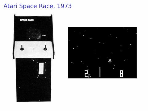
Atari Space Race, 1973

Atari Space Race PCB
Front Back (mirrored)

Read-Only Memories: Combinational Functions
2k × nROM
A0
A1
A2
...
Ak−1
D0
D1
...
Dn−1
General ROM:2k words
n bits per word
128× 1ROM
A0
A1
A2
A3
A4
A5
A6
D
Example:Space Race ROM
column
row

Implementing ROMs
0/1
0
Z: “notconnected”
0
1
0
1
1
1
Add. Data
00 01101 11010 10011 010
2-to-4Decoder
A1A0
0 1 1
1 1 0
1 0 0
0 1 0
Wordline 00
Wordline 11
Wordline 22
Wordline 33
Bitline 0
D0
Bitline 1
D1
Bitline 2
D2

Implementing ROMs
0/1
0
Z: “notconnected”
0
1
0
1
1
1
Add. Data
00 01101 11010 10011 010
2-to-4Decoder
1A10A0
0 1 1
1 1 0
1 0 0
0 1 0
Wordline 00
Wordline 11
Wordline 22
Wordline 33
Bitline 0
D0
Bitline 1
D1
Bitline 2
D2
1 0 0
0
0
1
0

Implementing ROMs
0/1
0
Z: “notconnected”
0
1
0
1
1
1
Add. Data
00 01101 11010 10011 010
2-to-4Decoder
A1A0
0
1
2
3
D0D1D2

Implementing ROMs
0/1
0
Z: “notconnected”
0
1
0
1
1
1
Add. Data
00 01101 11010 10011 010
2-to-4Decoder
A1A0
0
1
2
3
D0D1D2
0 01
1
1
0
1

Atari Space Race Schematic

The 1971 DEC M792-YB Bootstrap Diode Matrix
32-word, 16-bit (64-byte) ROM diode matrix
CMOS Mask-Programmed ROMs
Add. Data
00 01101 11010 10011 010
ROM “programmed”by selectivelyconnecting drainwires
Active-highwordlines

Mask ROM Die Photo

Color PROM in Pac-Man
00 0001 0702 6603 EF04 0005 F806 EA07 6F08 0009 3F0A 000B C90C 380D AA0E AF0F F610 00...
...1F 00

A Floating Gate MOSFET
Cross section of a NOR FLASH transistor. Kawai et al., ISSCC 2008 (Renesas)

Floating Gate n-channel MOSFET
Channel
Drain Source
Floating Gate
Control GateSiO2
Floating gate uncharged; Control gate at 0V: Off

Floating Gate n-channel MOSFET
Channel
Drain Source
Floating Gate
Control GateSiO2+++++++++
−−−−−−−−+++++++++
−−−−−−−−
Floating gate uncharged; Control gate positive: On

Floating Gate n-channel MOSFET
Channel
Drain Source
Floating Gate
Control GateSiO2
−−−−
−−−−++++
++++
Floating gate negative; Control gate at 0V: Off

Floating Gate n-channel MOSFET
Channel
Drain Source
Floating Gate
Control GateSiO2++++++++
−−−−−−−
−−++
Floating gate negative; Control gate positive: Off

EPROMs and FLASH use Floating-Gate MOSFETs

Static Random-Access Memory Cell
Word line
Bit line Bit line

Layout of a 6T SRAM Cell
��
���
!� !�$%� $%�&$
'()�
�����"#�����
Weste and Harris. Introduction to CMOS VLSI Design.Addison-Wesley, 2010.

Intel’s 2102 SRAM, 1024 × 1 bit, 1972

2102 Block Diagram

SRAM Timing
A12A11
A2A1A0
CS2
D7D6
D1D0
......
CS1
WEOE
62648K × 8SRAM
CS1
CS2
WE
OE
Addr 1 2
Data write 1 read 2

6264 SRAM Block Diagram
CY6264-1
A1A2A3A4A5A6A7A8
I/O0
256 x 32 x 8ARRAY
INPUT BUFFER
COLUMN DECODERPOWERDOWN
I/O1
I/O2
I/O3
I/O4
I/O5
I/O6
I/O7CE1CE2WE
OE

Galaga CPU detail (Namco/Midway 1981)

Dynamic RAM Cell
Word line
Bit line

Our Old Pal, the Space Race ROM0
1
2
3
4
5
6
7
8
9
10
11
12
13
14
15
A0A1A2A3 D0 D1 D2 D3 D4 D5 D6 D7
means
and
means

Our Old Pal, the Space Race ROM0
1
2
3
4
5
6
7
8
9
10
11
12
13
14
15
A0A1A2A3 D0 D1 D2 D3 D4 D5 D6 D7
The decoder or“AND plane”
In a RAM or ROM,computes everyminterm
Pattern is notprogrammable

Our Old Pal, the Space Race ROM0
1
2
3
4
5
6
7
8
9
10
11
12
13
14
15
A0A1A2A3 D0 D1 D2 D3 D4 D5 D6 D7
The decoder or“OR plane”
One term for everyoutput
Pattern isprogrammable =the contents of theROM

Our Old Pal, the Space Race ROM0
1
2
3
4
5
6
7
8
9
10
11
12
13
14
15
A0A1A2A3 D0 D1 D2 D3 D4 D5 D6 D7
Can we do better?

Simplifying the Space Race ROM
0 0 0 00 0 0 00 1 0 00 0 0 0
A0
A1
A2A3
0 0 0 00 0 0 01 1 0 00 0 0 0
0 0 0 00 0 0 00 1 0 00 0 1 0
0 0 0 01 0 0 00 1 1 10 0 0 1
0 0 1 01 0 0 00 0 1 00 1 0 0
0 0 0 11 1 1 10 1 1 11 0 0 0
0 1 0 00 0 0 00 1 0 00 0 0 0
1 0 0 00 0 0 00 1 0 00 0 0 0
Essential minterms mean don’t expand these

Our New PAL, the Space Race ROM0
1
2
3
4
5
6
7
8
9
10
11
12
13
14
15
A0A1A2A3 D0 D1 D2 D3 D4 D5 D6 D7
3210D0=3210
D1=321
D2=3210+ 3210
D3=3210+ 310+3210+ 3210
D4=3210+ 3210+3210+ 3210
D5=310+ 20+ 21+3210+ 3210
D6=3210+ 3210
D7=3210+ 3210
Saved two ANDs

Our New PAL, the Space Race ROM0
1
2
3
4
5
6
7
8
9
10
11
12
13
14
15
A0A1A2A3 D0 D1 D2 D3 D4 D5 D6 D7
3210
321D0=3210
D1=321
D2=3210+ 3210
D3=3210+ 310+3210+ 3210
D4=3210+ 3210+3210+ 3210
D5=310+ 20+ 21+3210+ 3210
D6=3210+ 3210
D7=3210+ 3210
Saved two ANDs

Our New PAL, the Space Race ROM0
1
2
3
4
5
6
7
8
9
10
11
12
13
14
15
A0A1A2A3 D0 D1 D2 D3 D4 D5 D6 D7
3210
321
3210
D0=3210
D1=321
D2=3210+ 3210
D3=3210+ 310+3210+ 3210
D4=3210+ 3210+3210+ 3210
D5=310+ 20+ 21+3210+ 3210
D6=3210+ 3210
D7=3210+ 3210
Saved two ANDs

Our New PAL, the Space Race ROM0
1
2
3
4
5
6
7
8
9
10
11
12
13
14
15
A0A1A2A3 D0 D1 D2 D3 D4 D5 D6 D7
3210
321
3210
3210
310
3210
D0=3210
D1=321
D2=3210+ 3210
D3=3210+ 310+3210+ 3210
D4=3210+ 3210+3210+ 3210
D5=310+ 20+ 21+3210+ 3210
D6=3210+ 3210
D7=3210+ 3210
Saved two ANDs

Our New PAL, the Space Race ROM0
1
2
3
4
5
6
7
8
9
10
11
12
13
14
15
A0A1A2A3 D0 D1 D2 D3 D4 D5 D6 D7
3210
321
3210
3210
310
3210
3210
3210
D0=3210
D1=321
D2=3210+ 3210
D3=3210+ 310+3210+ 3210
D4=3210+ 3210+3210+ 3210
D5=310+ 20+ 21+3210+ 3210
D6=3210+ 3210
D7=3210+ 3210
Saved two ANDs

Our New PAL, the Space Race ROM0
1
2
3
4
5
6
7
8
9
10
11
12
13
14
15
A0A1A2A3 D0 D1 D2 D3 D4 D5 D6 D7
3210
321
3210
3210
310
3210
3210
3210
310
20
21
3210
3210
3210
D0=3210
D1=321
D2=3210+ 3210
D3=3210+ 310+3210+ 3210
D4=3210+ 3210+3210+ 3210
D5=310+ 20+ 21+3210+ 3210
D6=3210+ 3210
D7=3210+ 3210
Saved two ANDs

A 22V10 PAL: Programmable AND/Fixed OR0 4 8 12 16 20 24 28
Increments
FirstFuseNumbers
32 36 40
Macro-cell
R = 5809P = 5808
R = 5811P = 5810
R = 5813P = 5812
R = 5815P = 5814
R = 5817P = 5816
Asynchronous Reset
23
22
21
20
19
1
2
3
4
5
(to all registers)
396
0
440
880
924
1452
1496
2112
2156
2860
I/O/Q
I/O/Q
I/O/Q
I/O/Q
I/O/Q
I
I
I
I
CLK/I
Macro-cell
Macro-cell
Macro-cell
Macro-cell

Field-Programmable Gate Arrays (FPGAs)
Switch BlockLE LE LE
SB SB
LE LE LE
LUT
16×1 RAMprogrammable switch
Switch Box: 6programmable
switches