fundamentals of signal and power integrity - …emc/20130530p1.pdf · fundamentals of signal and...
TRANSCRIPT
Fundamentals of Signal and Power Integrity
Christian Schuster
Distinguished Lecturer for the IEEE EMC Society 2012-13
Institute of Electromagnetic Theory
Hamburg University of Technology (TUHH)

Christian Schuster – 2
Acknowledgements
Renato Rimolo-Donadio, Xiaomin Duan,
Sebastian Müller, Miroslav Kotzev,
Heinz-Dietrich Brüns
Young Kwark, Xiaoxiong Gu, Mark Ritter,
Bruce Archambeault, Dale Becker,
Thomas-Michael Winkel, Hubert Harrer
… and many others!
Christian Schuster – 3
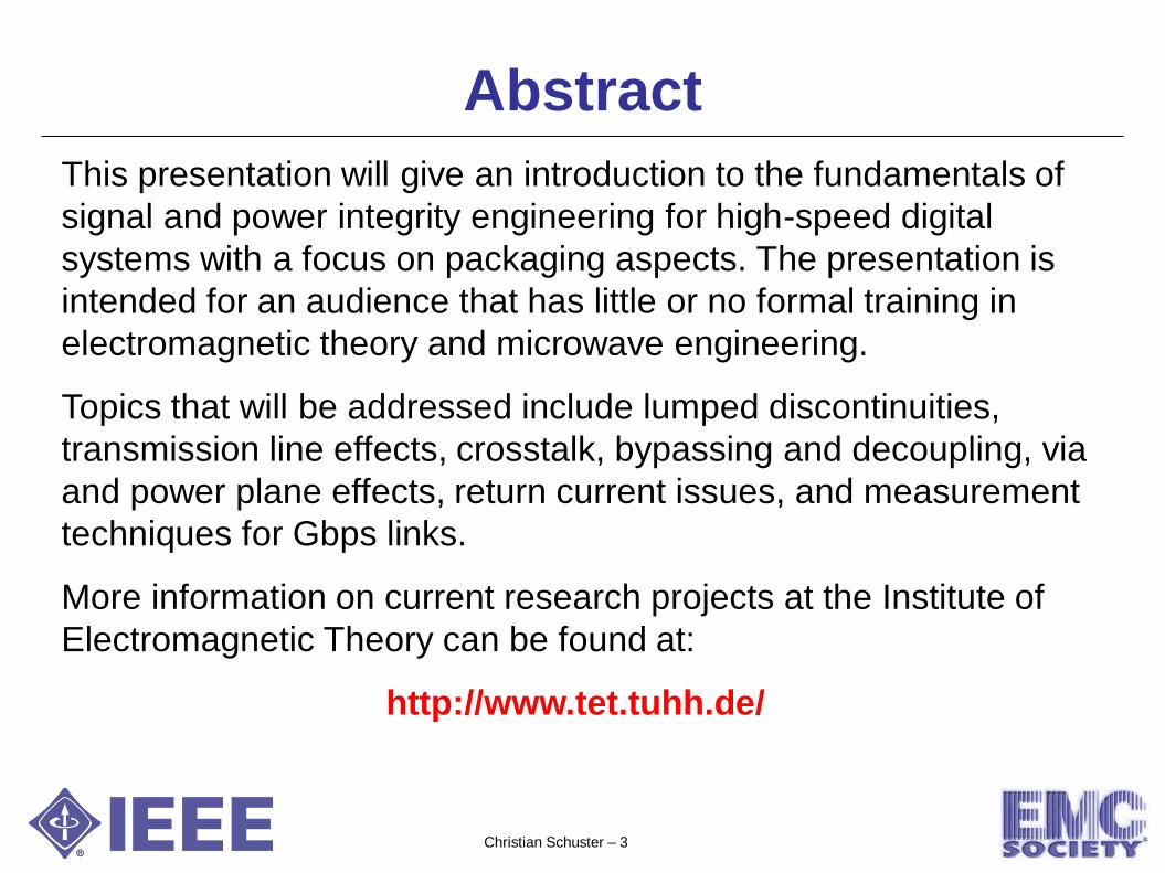
Abstract
This presentation will give an introduction to the fundamentals of
signal and power integrity engineering for high-speed digital
systems with a focus on packaging aspects. The presentation is
intended for an audience that has little or no formal training in
electromagnetic theory and microwave engineering.
Topics that will be addressed include lumped discontinuities,
transmission line effects, crosstalk, bypassing and decoupling, via
and power plane effects, return current issues, and measurement
techniques for Gbps links.
More information on current research projects at the Institute of
Electromagnetic Theory can be found at:
http://www.tet.tuhh.de/

Christian Schuster – 4
Power Plane Ground Plane
Driver Via
Receiver
A Bird‘s Eye View on SI, PI & EMC
DC Power Supply
PCB

Christian Schuster – 5
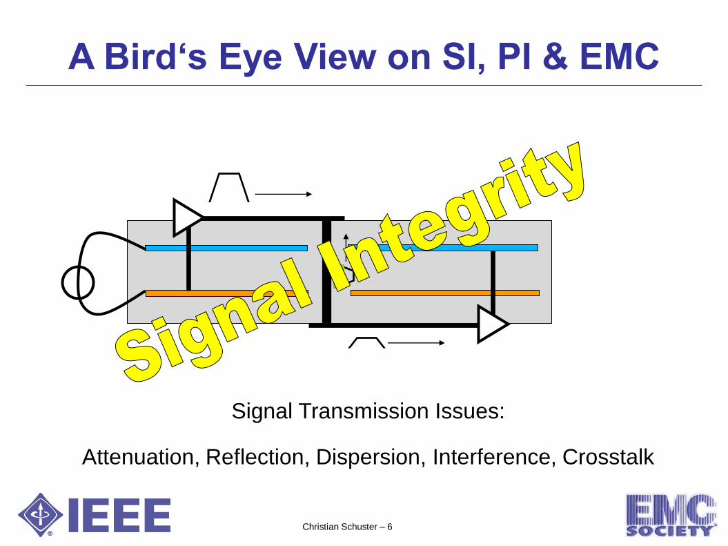
A Bird‘s Eye View on SI, PI & EMC
Signal Transmission Issues:
Attenuation, Reflection, Dispersion, Interference, Crosstalk
Christian Schuster – 6
A Bird‘s Eye View on SI, PI & EMC
Signal Transmission Issues:
Attenuation, Reflection, Dispersion, Interference, Crosstalk

Christian Schuster – 7
A Bird‘s Eye View on SI, PI & EMC
Power Delivery Issues:
Voltage Drop, Switching Noise, Crosstalk

Christian Schuster – 8
A Bird‘s Eye View on SI, PI & EMC
Power Delivery Issues:
Voltage Drop, Switching Noise, Crosstalk

Christian Schuster – 9
A Bird‘s Eye View on SI, PI & EMC
Electromagnetic Compatibility Issues:
Near Field Coupling, Radiated Emissions

Christian Schuster – 10
A Bird‘s Eye View on SI, PI & EMC
Electromagnetic Compatibility Issues:
Near Field Coupling, Radiated Emissions

Christian Schuster – 11
SI + PI + EMC = “Electrical Integrity“

Christian Schuster – 12
(1) Hamburg and TUHH
(2) Signal Integrity
(3) Power Integrity
(4) Vias and Return Currents
(5) Measurement Techniques
(6) Wrapping Up
Outline

Christian Schuster – 13
(1)
Hamburg and TUHH

Christian Schuster – 14

Christian Schuster – 15
Hamburg University of Technology © TUHH
Downtown
Founded 1978
Approx. 6000 Students
Approx. 100 Faculty Members

Christian Schuster – 16
Hamburg University of Technology © TUHH

Christian Schuster – 17
D
0 B
t
BE
t
DJH
Printed circuit board layout
Maxwell‘s Equations
What We Do at TUHH

Christian Schuster – 18
(2)
Signal Integrity

Christian Schuster – 19
Electrical Integrity of Digital Systems

Christian Schuster – 20
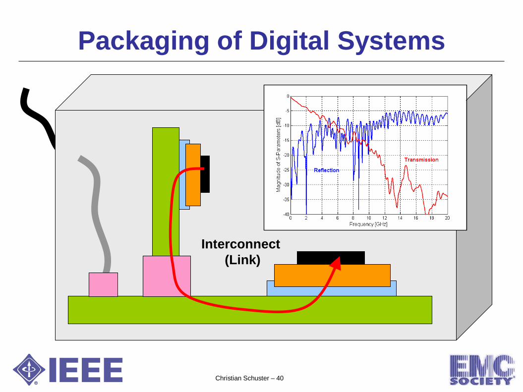
Packaging of Digital Systems
Housing / Chassis
Connector
Package / Module
IC (Transmitter)
IC (Receiver)
Connector
Cable
Backplane / Motherboard
Socket
Dau
gh
terc
ard

Christian Schuster – 21
Packaging of Digital Systems
Connector
Interconnect
(Link)

Christian Schuster – 22
The ideal interconnect will simply delay the signal:
Any real interconnect will additionally change timing and amplitude:
t
Tx Rx
t
Tx Rx
Effect of Interconnects

Christian Schuster – 23
Effect of Interconnects
The deviations in timing and amplitude are in general called:
t
Timing jitter or simply: JITTER
Amplitude noise or simply: NOISE

Christian Schuster – 24
Signal Bandwidth
s
)(ts
t
2/s
RTBT
timerise
5.0..3.01
R
max T
f
periodbit
5.0
2
1
B
0 T
f
Maximum Frequency
Fundamental Frequency

Christian Schuster – 25
Maintaining Signal Integrity
1. Match terminations
2. Manage discontinuities
3. Reduce Coupling
4. Limit attenuation
5. Equalize signals
Christian Schuster – 26
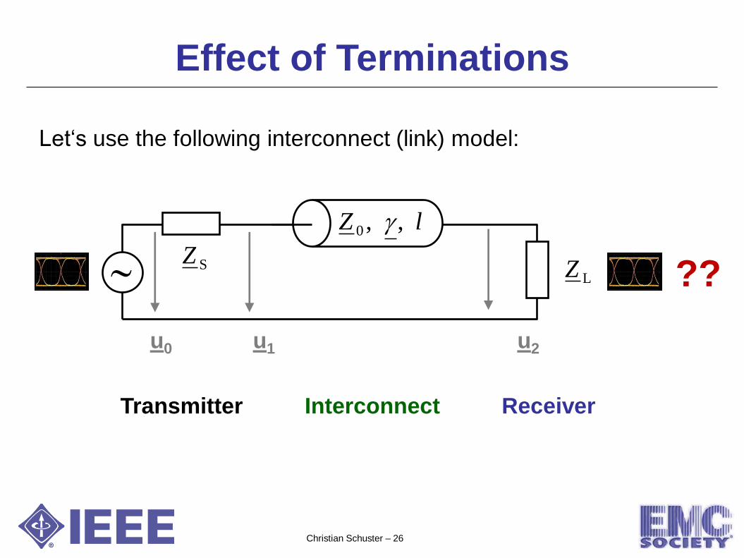
Effect of Terminations
Let‘s use the following interconnect (link) model:
lZ ,,0
u0 u1 u2
LZSZ
Transmitter Receiver Interconnect
??

Christian Schuster – 27
Metal Dielectric
Microstrip
Line
Stripline
(symmetric)
(h = height of dielectric,
w = conductor width,
t = conductor thickness)
tw
hZ
8.0
98.5ln
41.1
87
r
0
tw
hZ
8.0
9.1ln
60
r
0
(h = height of dielectric,
w = conductor width,
t = conductor thickness)
Transmission Lines in Digital Systems

Christian Schuster – 28
Typical trace length
≈ 5 – 75 cm
Velocity of propagation
≈ 150 000 km/s
Operating frequency
≈ 5 GHz
Corrsponding wavelength
≈ 3 cm
…
up to 25 wavelengths on a trace!
Delay ≈ 5 ns
Transmission Lines in Digital Systems
Printed circuit board layout

Christian Schuster – 29
Let‘s use the following interconnect (link) model:
lZ ,,0
u0 u1 u2
LZSZ??
!max. and const.0
2 u
u
Effect of Terminations

Christian Schuster – 30
lZ ,,0
LZSZ
input acceptance
0S
0
ZZ
Za
Effect of Terminations

Christian Schuster – 31
lZ ,,0
LZSZ
input acceptance TL transfer function
)exp( lH
Effect of Terminations

Christian Schuster – 32
lZ ,,0
LZSZ
input acceptance TL transfer function
load transmission
load reflection
LL 1 rt
0L
0LL
ZZ
ZZr
Effect of Terminations

Christian Schuster – 33
lZ ,,0
LZSZ
input acceptance TL transfer function
source transmission load transmission
source reflection load reflection
0S
0SS
ZZ
ZZr
SS 1 rt
Effect of Terminations

Christian Schuster – 34
lZ ,,0
LZSZ
??1 SL
2
L
0
2
rrH
tHa
u
u
Effect of Terminations

Christian Schuster – 35
Hu
u
2
1
0
2 0LS ZZZ
lZ ,,0
LZSZ
0L ZZ Hau
u
0
2
Effect of Terminations
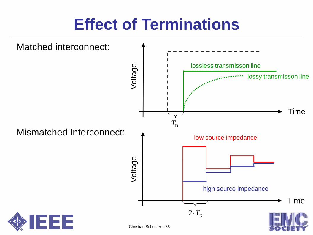
Christian Schuster – 36
Matched interconnect:
Mismatched Interconnect:
Time
low source impedance
high source impedance
D2 T
Time
Voltage
lossless transmisson line
Voltage
DT
lossy transmisson line
Effect of Terminations

Christian Schuster – 37
3
4
2
5 6
1
1 kΩ1,Ω50,Ω10 L0S ZZZ
zero losses
2 Ω100,Ω50,Ω50 L0S ZZZ
zero losses
3 Ω50,Ω50,Ω50 L0S ZZZ
zero losses
4 Ω100,Ω50,Ω100 L0S ZZZ
zero losses
kΩ1,Ω50,Ω10 L0S ZZZ
non-zero losses
5
6 Ω50,Ω50,Ω50 L0S ZZZ
non-zero losses
(all lines have a delay of 0.1 ns)
Effect of Terminations

Christian Schuster – 38
Matching Terminations
Check your interconnect length !
Check your interconnect impedance!
Match receiver input impedance!
Match transmitter output impedance!
!
)2( RD TT

Christian Schuster – 39
Tx
The technology is typically CMOS with the links being voltage
mode, unidirectional, serial, point-to-point, and source-
synchronous. For improved bandwidth equalization is typically used
in the Tx, Rx, or both.
CDR
.
.
.
Deserializer
Clock & Data Recovery
Data .
.
.
Serializer
Data
Clock
Equalizer
Equalizer
+ Slicer
Rx
Real World Interconnect (Link)
Christian Schuster – 40
Packaging of Digital Systems
Connector
Interconnect
(Link)

Christian Schuster – 41
Effect of Lumped Discontinuities
Signal
Out Signal
In
u1 u2 50
50 2.5
nH
Tx-Output Bond Wire Rx-Input
Source
Voltage
Received
Voltage

Christian Schuster – 42
Effect of Lumped Discontinuities
u1 u2
Signal
In Signal
Out
50 50 1 pF
Tx-Output Via Rx-Input
Source
Voltage
Received
Voltage

Christian Schuster – 43
Effect of Lumped Discontinuities
Attenuation of high frequency signal components
„Slowing down" of the edges of a digital signal
Frequency [GHz] Time [ps]
Magnitude o
f u
2 / u
1
u2(t
) / u
1(t
)
Frequency Response Step Response
f0 ≈ 6.37 GHz t 1/w0 = 25 ps

Christian Schuster – 44
Effect of Distributed Discontinuities
lZ ,, 0Z0Z
GHzl
cf 952.2
4
1 inch, 45 Ohm mismatched transmission line at c0 /2
Frequency Response
(Scattering Parameters)
Christian Schuster – 45
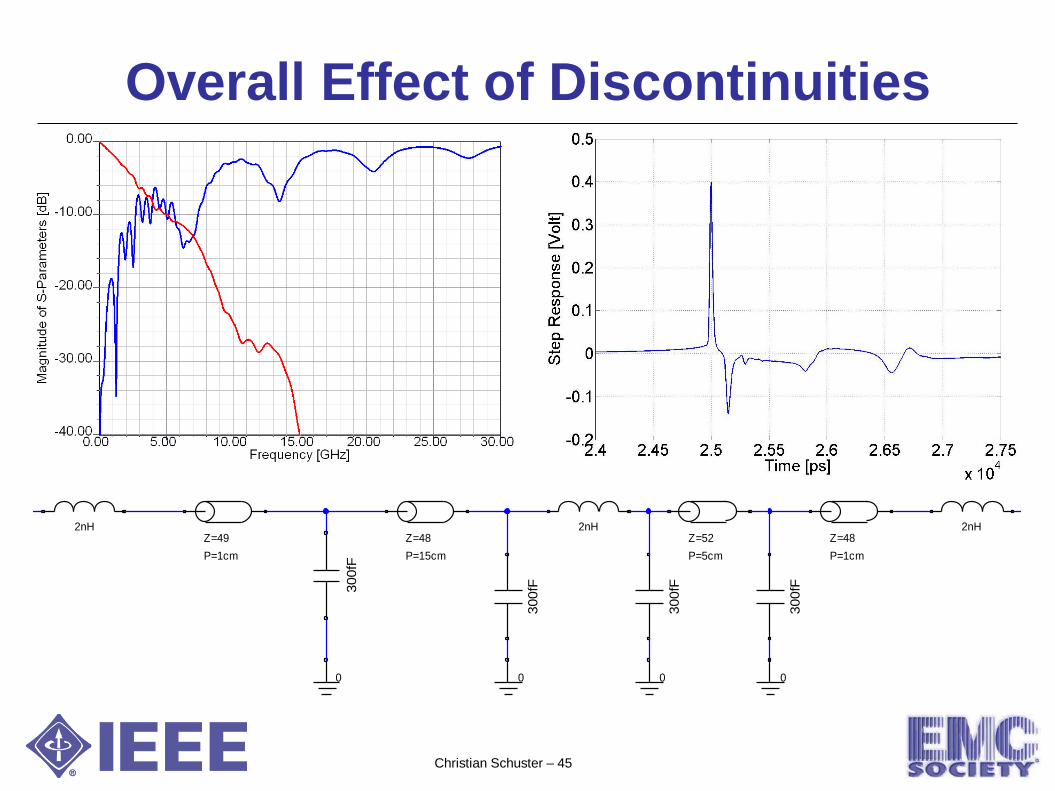
Overall Effect of Discontinuities
0 0 0 0
Port1 Port2
Z=49
P=1cm
300fF
2nHZ=48
P=15cm
300fF
2nH
300fF
Z=52
P=5cm
300fF
Z=48
P=1cm
2nH

Christian Schuster – 46
Managing Discontinuities
Avoid them!
Check their impact!
Minimize them (± 10 Ohm around 50 Ohm)!
Compensate them (difficult)!
Concentrate on the “bottleneck!
!

Christian Schuster – 47
Packaging of Digital Systems
Connector
Interconnect
(Link)

Christian Schuster – 48
(3) Near End (4) Far End
Aggressor Line (Active Line)
Victim Line (Quiet Line)
(1) Input (2) Output
Effect of Coupling
Consider two transmission lines in close proximity:

Christian Schuster – 49
UL
IC
(3) Near End (4) Far End
(1) Input (2) Output
NEXT =
Near End Crosstalk (sum of ind. and cap. crosstalk)
FEXT =
Far End Crosstalk (difference of ind. and cap. crosstalk)
Consider two transmission lines in close proximity:
Effect of Coupling

Christian Schuster – 50
(3) Near End (4) Far End
For weak coupling (kL,C ≤ 0.25) it is found approximatively:
(1) Input (2) Output
RT
DT
DTRD TT
RD2 TT
Polarity also depends
on coupling coefficients. Polarity is equal
to input polarity.
Effect of crosstalk
is usually small. INPUT
maxU
RT
Effect of Coupling

Christian Schuster – 51
It should be noted that these formulas do not take into account losses
on the lines or reflections from load mismatches.
)5.0(4
)5.0(2
RD
INPUT
maxLC
RD
INPUT
max
R
DLC
NEXT
max
TTUkk
TTUT
Tkk
U
INPUT
max
R
DLCFEXT
max2
UT
TkkU
Effect of Coupling
For weak coupling (kL,C ≤ 0.25) it is found approximatively:

Christian Schuster – 52
Example for Coupling Coefficients
h
a
diameter = d
0
For two thin wires above infinite ground one can find:
1211
12C
CC
Ck
)/4ln(2
))/2(1ln( 2
dh
ah

Christian Schuster – 53
Reducing Coupling
Increase line separation!
Decrease distance to ground!
Balance capacitive and inductive coupling!
Increase rise time!
Reduce coupling length!
Use differential signaling!
!

Christian Schuster – 54
In a SINGLE-ENDED link
there is a common
(global) reference against
which the signal is
measured ("ground").
In a DIFFERENTIAL link
the reference is the
negative of the signal
itself (which has to be
transmitted as well).
Differential Signaling

Christian Schuster – 55
(3)
Power Integrity

Christian Schuster – 56
Electrical Integrity of Digital Systems

Christian Schuster – 57
Effect of Common Power Delivery
IC #1 IC #2
U0
ZPDN
PDN = Power Delivery Network

Christian Schuster – 58
Effect of Common Power Delivery
U0
R uIC L
iGate1, iGate2, …
Du
uIC = U0 - Du
...)()(...)()()( Gate1Gate1Gate1Gate1 D titidt
dLtitiRtu
"DC-drop or IR-drop" "DI-drop or DI-noise"

Christian Schuster – 59
Maintaining Power Integrity
1. Decrease PDN impedance
2. Add decoupling
3. Add even more decoupling
4. Use several power supplies
5. Use on-chip VRMs

Christian Schuster – 60
Discrete
Decoupling
Capacitors
(various sizes)
IC incl.
Power/Ground Grid
& Integrated Decaps
Printed Circuit Board incl.
Power/Ground Planes
High Power
DC Supply
Voltage
Regulator
Module
Package incl.
Power/Ground
Planes
PDN Elements

Christian Schuster – 61
PDN Impedance
In frequency domain the standard PDN model looks like this:
ZPDN ( f )
u0 ZIC ( f )
max)( ufu DD
Du( f ) ~
TargetPDN )( ZfZ
range"frequency operating" f

Christian Schuster – 62
A typical maximum ripple for ditigal systems is:
With a 10% value the following numbers can be obtained for
applications … of the early 1990'ies: … of 2000 and on:
PDN Impedance
Ω5.0
W5
Ω0.5/
A1
V0.5
Target
avg
avg0
avg
0
Z
P
iu
i
u
%10to%5ripple maximum0
max D
u
u
Ω001.0
W144
Ω01.0/
A120
V2.1
Target
avg
avg0
avg
0
Z
P
iu
i
u
= 1 m !

Christian Schuster – 63
Is 1 m hard to achieve? How about 10 m? Let's see …
Example:
The PDN consists of a simple copper wire of 2 mm radius in
theform of a flat rectangle with side lengths of 5 cm and 1 cm,
respectively.
It turns out that 10 m cannot be maintained beyond 40 kHz!
PDN Impedance
nH40m7.0with LR
22
PDN )( LRZ w

Christian Schuster – 64
Decreasing PDN Impedance
Use adequate copper cross sections!
Avoid big current loops!
Use power/ground planes!
Provide enough power/ground pins!
Decouple!
!

Christian Schuster – 65
Decoupling
Based on the simple example from before:
) largefor (
PDN
w
w
w
Lj
LjRZ
(R = 0.7
m,
L = 40 nH)
R L
U0 ~ ZIC ( f )

Christian Schuster – 66
… we ask what a so called "decoupling" or "bypass" capacitor does:
Decoupling
) largefor (1
1 2PDN
ww
ww
w
Cj
LCRCj
LjRZ
R L
U0 ~ ZIC ( f ) C
R = 0.7 m
L = 40 nH
C = 1 mF

Christian Schuster – 67
Heuristic explanation:
Frequency domain: Beyond the resonance frequency the capacitor
decouples the part of the PDN that lies "left" of him, i.e. the IC sees
only the impedance of the capacitor.
Time domain: The capacitor stores charges close to the IC that can
become currents needed for fast switching. It is like a "small battery".
Decoupling
R L
U0 ~ ZIC ( f ) C

Christian Schuster – 68
While being beneficial at higher
frequencies decoupling increases
the PDN impedance in the vicinity
of the resonance frequency:
Hence, increasing the "damping"
(by increasing R and/or reducing
L/C) can be helpful:
Decoupling
2
0
1R
C
L
Lw
*2)/( RCL
RC
L
RZ
1)( 0PDN w
m57)( 0PDN wZ
R = 0.7 m
L = 40 nH
C = 1 mF
R = 10 m
L = 40 nH
C = 1 mF
*)1becomescondition the//1with( QCLRQ
Christian Schuster – 69
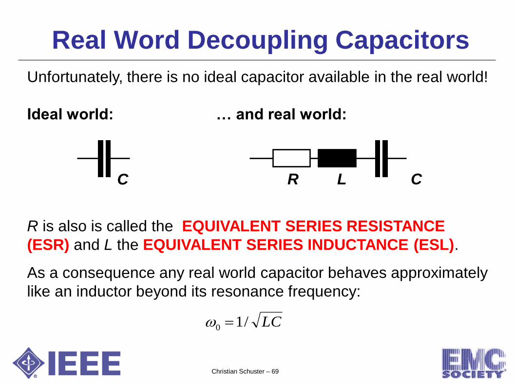
Unfortunately, there is no ideal capacitor available in the real world!
Ideal world: … and real world:
R is also is called the EQUIVALENT SERIES RESISTANCE
(ESR) and L the EQUIVALENT SERIES INDUCTANCE (ESL).
As a consequence any real world capacitor behaves approximately
like an inductor beyond its resonance frequency:
Real Word Decoupling Capacitors
C R L C
LC/10 w

Christian Schuster – 70
More Decoupling
Speed of charge
delivery,
effective
frequency
~
board-level package-level chip-level
Amount of
charge, size
of decoupling
capacitance

Christian Schuster – 71
Power/Ground Planes
Power/ground planes serve multiple purposes at the same time:
easy access to power and ground domains for mounted
components
a "natural" decoupling capacitor for PDN improvement
return current paths, i.e. they serve as reference conductors
shielding between different signal layers, i.e. they reduce
crosstalk
containment for internal EM fields, i.e. reduce EM emission
… HOWEVER …

Christian Schuster – 72
Power/Ground Planes
… they do show a resonant behavior:
11 inch
11 inch
10 mil Dielectric Filling
(r = 4) Port
(1 inch = 2.54 cm,
1 mil = 0.001 inch) nF11r0pp d
AC
Power
Ground
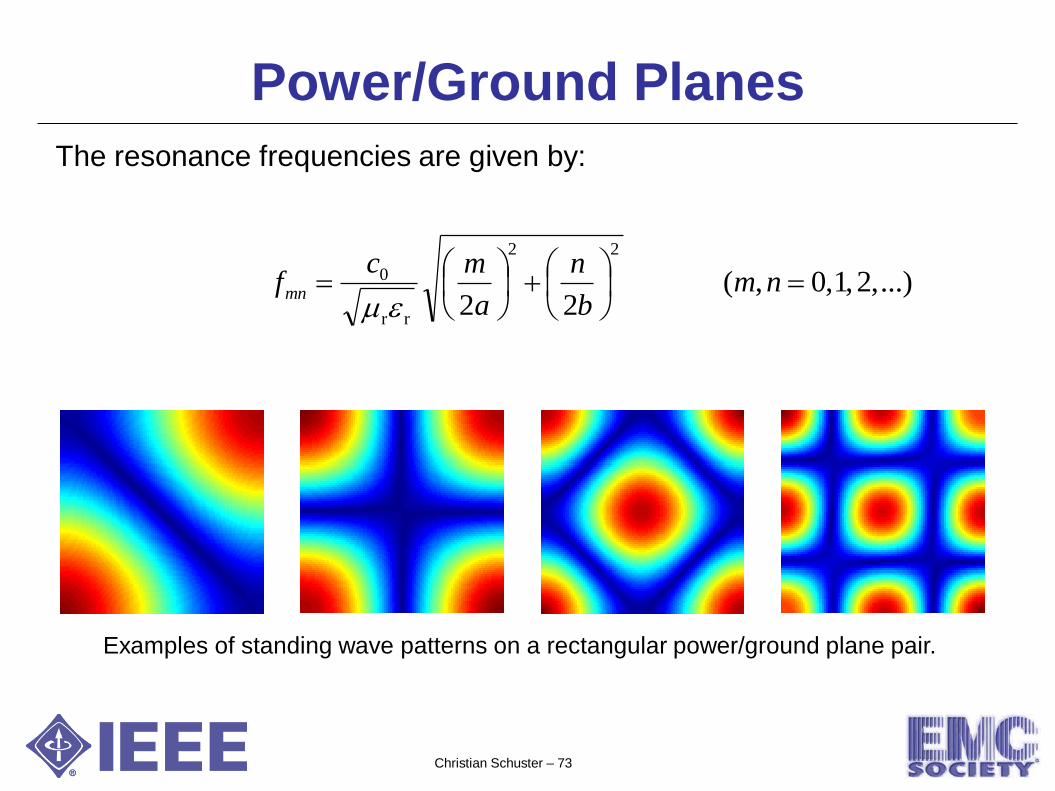
Christian Schuster – 73
...),2,1,0,(22
22
rr
0
nm
b
n
a
mcfmn
The resonance frequencies are given by:
Examples of standing wave patterns on a rectangular power/ground plane pair.
Power/Ground Planes

Christian Schuster – 74
Adding Decoupling
Determine your target impedance!
Determine your operating frequency range!
Provide decoupling at all levels/frequencies!
Use parallel decoupling to reduce ESR/ESL!
Be wary of resonances!
!

Christian Schuster – 75
(4)
Vias and Return Currents

Christian Schuster – 76
The Problem With Vias
Load
SignalVia
Signal Current
Load
Ground Via
Return Current

Christian Schuster – 77
A “Physcis-Based” Model for Vias
Via Cross Section
Zp
Zpp
Zp
viu
vil
iiu
iil
v'il
i'iu
i'il
vi
l
l
u
u
i
ipp
i
i
i
vZ
i
v
10
1
u
u
uu
u
i
i
pi
i
i
v
Zi
v
1/1
01
'
'
l
l
ll
l
i
i
pi
i
i
v
Zi
v
'
'
1/1
01Via
Plane
Plane Cp
Cp
Zpp:
(Parallel Plate
Impedance)
Current
Christian Schuster – 78
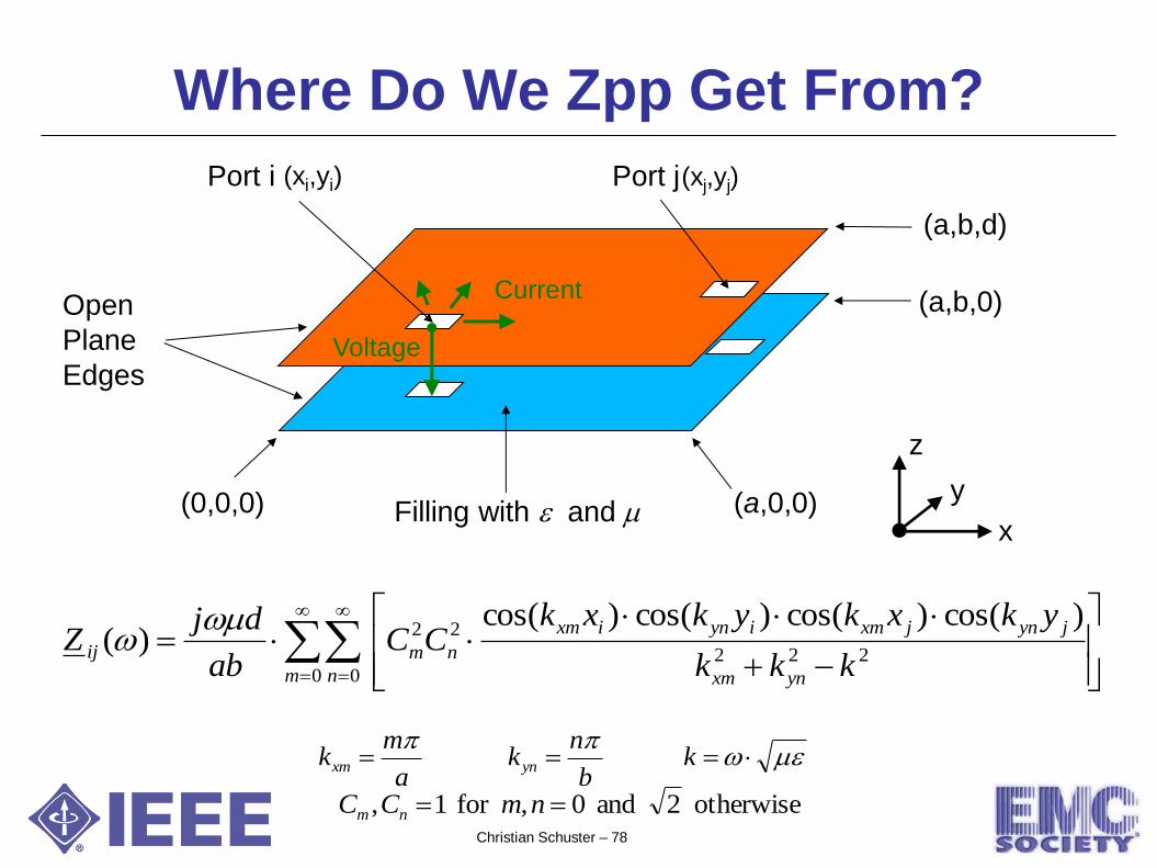
Where Do We Zpp Get From?
x
y
z
(0,0,0) (a,0,0)
(a,b,0)
(a,b,d)
Port i Port j (xi,yi)
Open
Plane
Edges Voltage
Current
(xj,yj)
Filling with and
0 0222
22)cos()cos()cos()cos(
)(m n ynxm
jynjxmiynixm
nmijkkk
ykxkykxkCC
ab
djZ
ww
otherwise 2 and 0,for 1 , nmCC nm
w
kb
nk
a
mk ynxm

Christian Schuster – 79
Trace between planes:
2 Modes: Stripline + Parallel Plate
Modal decomposition: find suitable transformation
matrices to diagonalize MTL equations
Stripline Mode
Parallel Plate Mode (pp)
Including Striplines

Christian Schuster – 80
Including Striplines
2
1
2
1
22
22
2
1
2
1
)12()(
)(
gs
gs
ps
ps
ppstriplineppstripline
ppstriplineppstripline
gs
gs
ps
ps
V
V
V
V
YYkkYYkk
YYkkYYk
I
I
I
I
21
1
hh
hk
h2
h1
R. Rimolo-Donadio, H. D. Brüns, C. Schuster, “Including Stripline Connections into Network Parameter Based Via Models for
Fast Simulation of Interconnects,” International Zurich Symposium on Electromagnetic Compatibility, Switzerland, Jan. 12-15, 2009

Christian Schuster – 81
Decoupling capacitor model
Cavity
representation
S-Parameter
Matrix
Port 1 Port n
Cavities joined by
segmentation
techniques
R. Rimolo-Donadio et al., “Physics-based via and trace models for efficient link simulation on multilayer structures
up to 40 GHz", IEEE Trans. Microw. Theory and Techn., vol. 57, no. 8, p.p. 2072-2083, August 2009.
Zpp Ztl
Decap
Linterc. Decoupling capacitor model
Zpp Ztl
Decap
Linterc. Decoupling capacitor model Decap
Linterc. Decoupling capacitor model
Cavity
representation
Stacking the Deck

Christian Schuster – 82
6 Vias, 4 traces case
Centered striplines at two
levels, and thru vias in a 6
cavity stackup
Full-wave model
Mag
nit
ude
of
S1
2 [
dB
]
Frequency [GHz]
Model
FEM simulation
FIT simulation Full-wave model M
agnit
ud
e o
f S
14 [
dB
]
Frequency [GHz]
Model
FEM simulation
FIT simulation
Comparison with Full-Wave Results

Christian Schuster – 83
• 119 vias (76 signal,
43 ground)
• 14 differential
striplines (2D)
• 6 cavities
• Terminations
Comp. time: < 3 min
Assumption
of infinite
plates
Comparison with Measurements

Christian Schuster – 84
Models capture the salient features of the
hardware response despite the drastic
model simplification
|S13| [dB] - FEXT |S12| [dB] - IL
Link 10 -
S3 Stripline
Link 17 -
S5 Stripline
Link 10 -
S3 Stripline
Link 17 -
S5 Stripline
Measurement Link 10
Measurement Link 17
Model Link 10
Model Link 17
Comparison with Measurements

Christian Schuster – 85
Investigation of Via Return Currents
Effect of number
of ground vias:
6 GND vias 4 GND vias
2 GND vias 1 GND via
GND via

Christian Schuster – 86
Investigation of Via Return Currents
Effect of number
of ground vias:
Frequency [GHz]
Mag
nit
ud
e of
S12 [
dB
]
1 GND vias
2 GND vias
4 GND vias
6 GND vias

Christian Schuster – 87
(5)
Measurement Techniques

Christian Schuster – 88
Multiport Vector Network Analysis
Agilent Vector Network
Analyzer 8364C with
12-port extension at
Institute of Electromagnetic
Theory (TUHH)
12 ports
Bandwidth 10 MHz – 50 GHz
Electronic calibration module
Advanced calibration software

Christian Schuster – 89
Surface Connectors
STRUCTURE UNDER TEST
5 mm
STRUCTURE UNDER TEST
MICRO-PROBE Access Vias
5 mm
Common Surface Launches
... but vias are usually a high
frequency bottleneck !

Christian Schuster – 90
STRUCTURE
UNDER TEST
MICRO-
PROBE
MICRO-
PROBE Ground Vias
Ground pads with “U” strap
Signal trace
No access vias → less distortion → probes closer to the structure under test
The Recessed Probe Launch (RPL)

Christian Schuster – 91
Error boxes of RPLs from TRL calibration
(thru = 90 mil long, line = 220 mil long)
RPL Error Box Extraction

Christian Schuster – 92
Problems with Via Arrays
13
mm 45°
Via array
Via array
92
… many vias at tight pitch!
Christian Schuster – 93
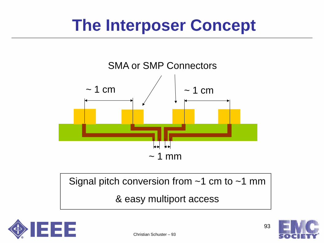
The Interposer Concept
~ 1 cm
SMA or SMP Connectors
~ 1 cm
~ 1 mm
Signal pitch conversion from ~1 cm to ~1 mm
& easy multiport access
93

Christian Schuster – 94
Typical Measurement Set-up
Multiport VNA
Interposer 1 Interposer 2
High speed serial links
94
Christian Schuster – 95
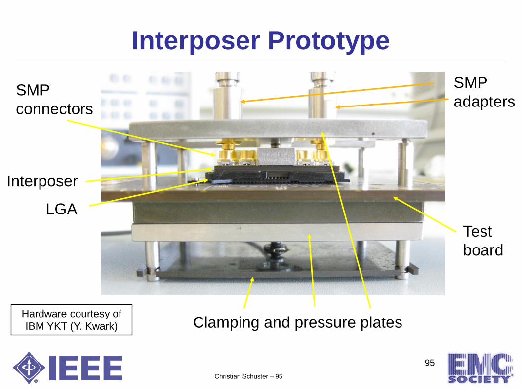
Interposer Prototype
95
Interposer
LGA
SMP
connectors
Test
board
Clamping and pressure plates
SMP
adapters
Hardware courtesy of
IBM YKT (Y. Kwark)

Christian Schuster – 96
Application to Link Measurement
1st interposer connected to
the via array 2nd interposer connected to the
via array
Stripline connecting vias
from both via arrays
96
Hardware courtesy of
IBM YKT (Y. Kwark)

Christian Schuster – 97
(6)
Wrapping Up

Christian Schuster – 98
Electrical Integrity of Digital Systems

Christian Schuster – 99
Electrical Integrity of Digital Systems
The basic goals of EMC, SI, and PI for an electrical system are
complementary to each other.
SIGNAL INTEGRITY: insure
acceptable quality of signals within
POWER INTEGRITY: insure
acceptable quality of power
delivery within
EMC: insure acceptable level of
interference with the outside
EMI
Frequency
Target
System
Frequency
PDN
Impedance
Target
System
SNR
Frequency
Target System

Christian Schuster – 100
Contact Information
Prof. Dr. sc. techn. Christian Schuster
Institut für Theoretische Elektrotechnik
Technische Universität Hamburg-Harburg
Harburger Schloss Str. 20
21079 Hamburg, Germany
Tel: +49 40 42878 3116
WWW: http://www.tet.tuhh.de/
E-Mail: [email protected]