fys3400 - vår 2020 (kondenserte fasers fysikk)
TRANSCRIPT
FYS3400 - Vår 2020 (Kondenserte fasers fysikk)http://www.uio.no/studier/emner/matnat/fys/FYS3410/v17/index.html
Pensum: Introduction to Solid State Physics
by Charles Kittel (Chapters 1-9 and 17 - 20)
Andrej Kuznetsov
delivery address: Department of Physics, PB 1048 Blindern, 0316 OSLO
Tel: +47-22857762,
e-post: [email protected]
visiting address: MiNaLab, Gaustadaleen 23a

2020 FYS3400 Lecture Plan (based on C.Kittel’s Introduction to SSP, Chapters 1-9, 17-20 + guest lectutes)
Module I – Periodity and Disorder (Chapters 1-3, 19, 20) calender week
To 16/1 12-13 Introduction.
On 22/1 10-12 Crystal bonding. Periodicity and lattices. Lattice planes and Miller indices. Reciprocal space. 4
To 23/1 12-13 Bragg diffraction and Laue condition
On 29/1 10-12 Ewald construction, interpretation of a diffraction experiment, Bragg planes and Brillouin zones 5
To 30/1 12-13 Surfaces and interfaces. Disorder. Defects crystals. Equilibrium concentration of vacancies
On 5/2 10-12 Mechanical properties of solids. Diffusion phenomena in solids; Summary of Module I 6
Module II – Phonons (Chapters 4, 5, and 18 pp.557-561)
To 6/2 12-13 Vibrations in monoatomic and diatomic chains of atoms; examples of dispersion relations in 3D
On 12/2 10-12 Lattice heat capacity: Dulong-Petit and Einstein models 7
To 13/2 12-13 Effect of temperature - Planck distribution;
On 19/2 10-12 canceled 8
To 20/2 12-13 Periodic boundary conditions (Born – von Karman); phonons and its density of states (DOS); Debye models
On 26/2 10-12 Comparison of different lattice heat capacity models; Thermal conductivity. 9
To 27/2 12-13 Thermal expansion
On 4/3 10-12 Summary of Module II 10
Module III – Electrons I (Chapters 6, 7, 11 - pp 315-317, 18 - pp.528-530, 19, and Appendix D)
To 5/3 12-13 Free electron gas (FEG) versus free electron Fermi gas (FEFG);
On 11/3 10-12 DOS of FEFG in 3D; Effect of temperature – Fermi-Dirac distribution. 11
To 12/3 12-13 canceled
teaching free week 12
Module IV – Disordered systems (guest lecture slides)
On 25/3 10-12 Thermal properties of glasses: Model of two level systems (Joakim Bergli) 13
To 26/3 12-13 Experiments in porous media (Gaute Linga)
On 1/4 10-12 Electron transport in disordered solids: wave localization and hopping (Joakim Bergli) 14
To 2/4 12-13 Theory of porous media (Gaute Linga)
Easter 15
Module V – Electrons II (Chapters 8, 9 pp 223-231, and 17, 19)
On 15/4 10-12 After Easter repetition; Heat capacity of FEFG in 3D 16
To 16/4 12-13 DOS of FEFG in 2D - quantum well, DOS in 1D – quantum wire, and in 0D – quantum dot
On 22/4 10-12 Origin of the band gap; Nearly free electron model; Kronig-Penney model 17
To 23/4 12-13 Effective mass method
On 29/4 10-12 Effective mass method for calculating localized energy levels for defects in crystals 18
To 30/4 12-13 Intrinsic and extrinsic electrons and holes in semiconductors
On 06/5 10-12 Carrier statistics in semiconductors 19
To 07/5 12-13 p-n junction
On 13/5 10-12 Summary of Modules III and V
To 14/5 12-13 Repetition - course in a nutshell
Exam: oral examination
May 28th – 29th

Lecture: P-N junction
• Repetition: intrinsic and extrinsic semiconductors
• Charge carrier transport mechanisms – diffusion and drift
• Band bending as a function of carrier concentration
• P-N junction in equilibrium
• Gauss and Poisson equations for the depletion region
•P-N junction with applied external bias

Intrinsic and extrinsic semiconductors
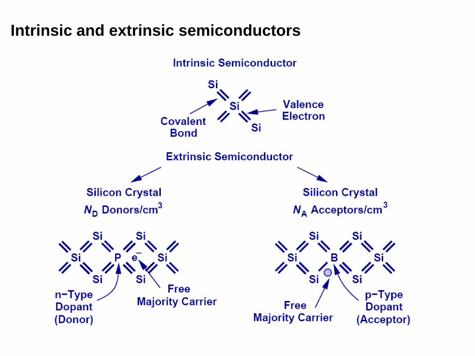
Summary of Charge CarriersIntrinsic and extrinsic semiconductors

Lecture: P-N junction
• Repetition: intrinsic and extrinsic semiconductors
• Charge carrier transport mechanisms – diffusion and drift
• Band bending as a function of carrier concentration
• P-N junction in equilibrium
• Gauss and Poisson equations for the depletion region
•P-N junction with applied external bias
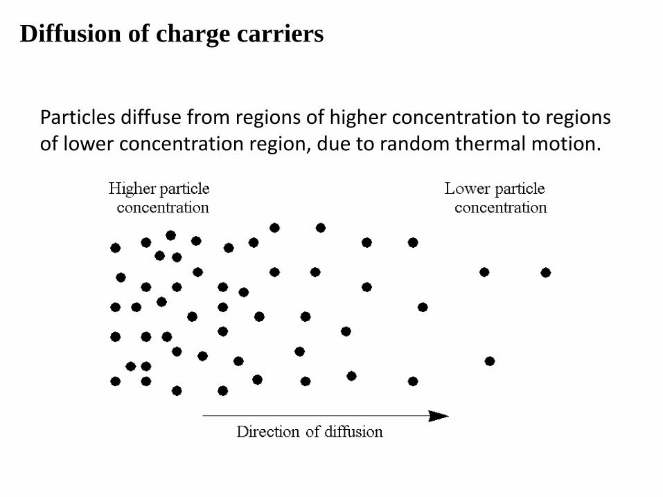
Particles diffuse from regions of higher concentration to regions of lower concentration region, due to random thermal motion.
Diffusion of charge carriers

dx
dnqDJ ndiffn,
dx
dpqDJ pdiffp,
D is the diffusion constant, or diffusivity.
Diffusion of charge carriers

• The process in which charge particles move because of an
electric field is called drift.
• Charge particles will move at a velocity that is proportional to
the electric field.
Ev
Ev
ne
ph
Drift of charge carriers

dx
dnqDqnJJJ nndiffndriftnn ε ,,
dx
dpqDqpJJJ ppdiffpdriftpp ε ,,
pn JJJ
Diffusion + drift of charge carriers

Lecture: P-N junction
• Repetition: intrinsic and extrinsic semiconductors
• Charge carrier transport mechanisms – diffusion and drift
• Band bending as a function of carrier concentration
• P-N junction in equilibrium
• Gauss and Poisson equations for the depletion region
•P-N junction with applied external bias

• The position of EF relative to the band edges is determined
by the carrier concentrations, which is determined by the
net dopant concentration.
• In equilibrium EF is constant; therefore, the band-edge
energies vary with position in a non-uniformly doped
semiconductor:
Ev(x)
Ec(x)
EF
Band bending as a function of carrier concentration
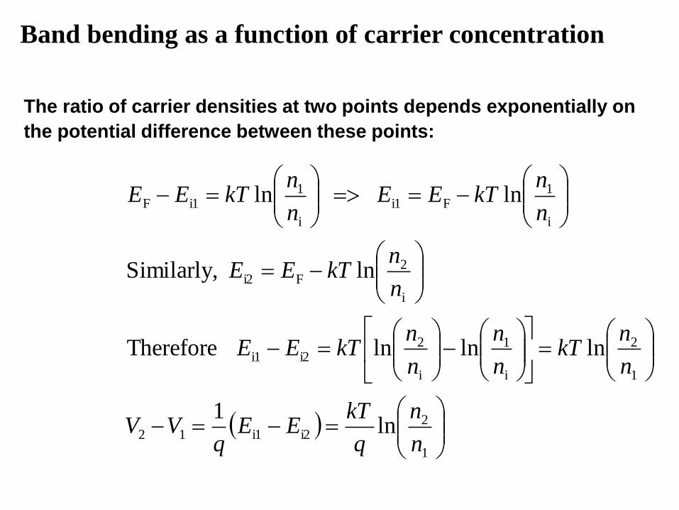
The ratio of carrier densities at two points depends exponentially on
the potential difference between these points:
1
2i2i112
1
2
i
1
i
2i2i1
i
2Fi2
i
1Fi1
i
1i1F
ln1
lnlnln Therefore
ln Similarly,
ln ln
n
n
q
kTEE
qVV
n
nkT
n
n
n
nkTEE
n
nkTEE
n
nkTEE
n
nkTEE
Band bending as a function of carrier concentration

dx
dEe
kT
N
dx
dn ckTEEc Fc /)(
dx
dE
kT
n c
kTEE
cFceNn
/)(
Ev(x)
Ec(x)
EF
εqkT
n
Band bending as a function of carrier concentration

Lecture: P-N junction
• Repetition: intrinsic and extrinsic semiconductors
• Charge carrier transport mechanisms – diffusion and drift
• Band bending as a function of carrier concentration
• P-N junction in equilibrium
• Gauss and Poisson equations for the depletion region
•P-N junction with applied external bias

<= P-type, low EF
- = fixed ionized acceptors
+ = mobile holes, p
<= N-type, high EF
+ = fixed ionized donors
- = mobile electrons, n
What happens when these bandstructures come into contact?
• Fermi energy must be constant at equilibrium, so bandsmust bend near the interface
• Far from the interface, bandstructures are conserved
P-N junctions in equilibrium

Time < 0
P-type piece N-type piece
Time < 0, i.e. before the contact is established
P-N junctions in equilibrium

At time = 0, slam the two pieces together
Time =0, the contact is “just” established
P-N junctions in equilibrium

Hole gradient
Jp, diffusion = -qDp dp/dx = current right, holes right
Electron gradient
Jn,diffusion = -qDn dn/dx = current right, electrons rightleft
P-N junctions in equilibrium
Question: How long this diffusion will og
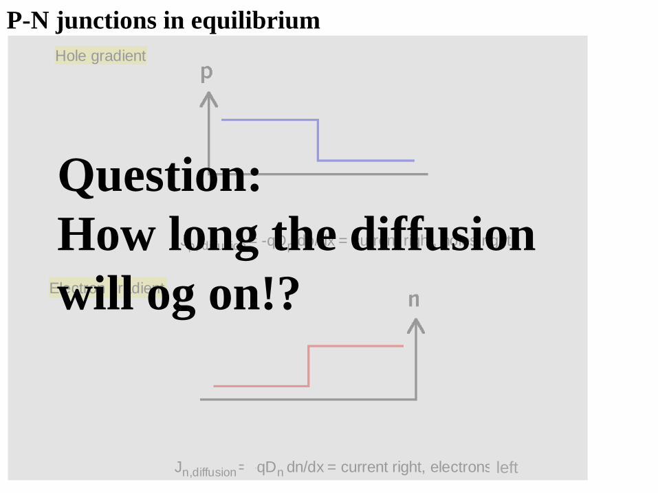
Hole gradient
Jp, diffusion = -qDp dp/dx = current right, holes right
Electron gradient
Jn,diffusion = -qDn dn/dx = current right, electrons rightleft
P-N junctions in equilibrium
Question:
How long the diffusion
will og on!?

• When the junction is first formed, mobile carriers diffuseacross the junction (due to the concentration gradients)
– Holes diffuse from the p side to the n side, leaving behind negatively charged immobile acceptor ions
– Electrons diffuse from the n side to the p side, leaving behind positively charged immobile donor ions
A region depleted of mobile carriers is formed at the junction.
• The space charge due to immobile ions in the depletion region establishes an electric field that opposes carrier diffusion.
+++++
––
–––
p n
acceptor ions donor ions
P-N junctions in equilibrium

P-N junctions in equilibrium

P-N junctions in equilibrium

E
E
Depletion Region
P-N junctions in equilibrium

How big is the built-in voltage?
RightiFLeftFibi EEEEqV )()(
P side N side
i
aLeftFi
kTEE
ia
a
n
NkTEE
enN
Np
Fi
ln)(
)(
i
dRightiF
kTEE
id
d
n
NkTEE
enN
Nn
iF
ln)(
)(
P-N junctions in equilibrium

2ln
lnln
i
dabi
i
d
i
abi
n
NN
q
kTV
n
N
q
kT
n
N
q
kTV
Na acceptor level on the p side
Nd donor level on the n side
How big is the built-in voltage?
P-N junctions in equilibrium

• One side of the junction is heavily doped, so that the Fermi level is close to the band edge.
• e.g. p+-n junction (heavy B implant into lightly doped Si substrate)
i
dGbi
i
DRightiF
GViLeftFi
n
N
q
kT
q
EV
n
NkTEE
EEEEE
ln2
ln)(
2/)(
P-N junctions in equilibrium

"P+ - N" => N a >> Nd => xp << xn
"P - N+" => N a << Nd => xp >> xn
P-N junctions in equilibrium

p-type n-type
DN AN
-
-
-
-
-
-
-
-
-
-
-
-
-
+++++++++++++
0E
biq
,p diffJ
,p driftJ
,n diffJ
,n driftJ
−
−
+
+
−
Thermal
generation
+
Thermal
generation
P-N junctions in equilibrium

Lecture: P-N junction
• Repetition: intrinsic and extrinsic semiconductors
• Charge carrier transport mechanisms – diffusion and drift
• Band bending as a function of carrier concentration
• P-N junction in equilibrium
• Gauss and Poisson equations for the depletion region
•P-N junction with applied external bias

neutral p region
+++++
––
–––
p n
acceptor ions donor ions
depletion region neutral n region
charge density (C/cm3)
distance
Charge is stored in the depletion region.
Gauss and Poisson equations for the depletion region

2
2
( ) ( ) ( )d x dE x x
dx dx
00
1( ) ( ) ( )
x
xE x E x x dx
dE
dx
1 encl
S V
QE dA dV
Gauss’s law describes the relationship between the charge density and the
electric field.
Poisson’s equation describes the relationship between the electric field
distribution and the electric potential
00( ) ( ) ( )
x
xx x E x dx
Gauss and Poisson equations in one dimension
Gauss and Poisson equations for the depletion region

0 ( ) ( ) ( 0)apo po
s
qNE x x x x x
000
0
0
0 , 0 and 0
0 np
nd
paxxxxx
xxqN
xxqNx
xno x
x
-xpo
ρo(x)
-qNa
qNd
xno x
x
-xpo
E0(x)
s
nod
s
poa xqNxqNE
)0(0
00 0
0
( )( ) ( ) ( ) 0
( ) ( )
(0 )
noxd
no nox
s s
dno
s
no
x qNE x dx E x x x
qNE x x x
x x
Gauss’s Law
p n
p n
Gauss and Poisson equations for the depletion region

pn
x
E0(x)
s
nod
s
poa xqNxqNE
)0(0
xno-xpo
22
22 pos
a
nos
dx
qNx
qN
0(x)
xxno-xpo
Poisson’s Equation
Gauss and Poisson equations for the depletion region

Lecture: P-N junction
• Repetition: intrinsic and extrinsic semiconductors
• Charge carrier transport mechanisms – diffusion and drift
• Band bending as a function of carrier concentration
• P-N junction in equilibrium
• Gauss and Poisson equations for the depletion region
•P-N junction with applied external bias

• The quasi-neutral p and n regions have low resistivity, whereas the depletion region has high resistivity. Thus, when an external voltage VD is applied across the diode, almost all of this voltage is dropped across the depletion region.
• If VD > 0 (forward bias), the potential barrier to carrier diffusion is reduced by the applied voltage.
• If VD < 0 (reverse bias), the potential barrier to carrier diffusion is increased by the applied voltage.
p n
+++++
––
–––
VD
P-N junction with applied external bias

pn
x
E0(x)
s
nod
s
poa xqNxqNE
)0(0
xno-xpo
22
22 pos
a
nos
dx
qNx
qN
0(x)
xxno-xpo
bi
Built-in potential bi=
-xp xn
-xp xn
bi-qVD
Higher barrier leads to less current!
P-N junction with applied external bias

pn
x
E0(x)
s
nod
s
poa xqNxqNE
)0(0
xno-xpo
22
22 pos
a
nos
dx
qNx
qN
0(x)
xxno-xpo
bi
Built-in potential bi=
-xp xn
bi-qVD
Lower barrier lead to more current!
-xp xn
P-N junction with applied external bias

• As VD increases, the potential barrier to carrier
diffusion across the junction decreases*, and
current increases exponentially.
ID (Amperes)
VD (Volts)
* Hence, the width of the depletion region decreases.
p n
+++++
––
–––
VD > 0The carriers that diffuse across the
junction become minority carriers in
the quasi-neutral regions; they then
recombine with majority carriers,
“dying out” with distance.
D( 1)qV kT
D SI I e
P-N junction with applied external bias

• As |VD| increases, the potential barrier to carrier
diffusion across the junction increases*; thus, no
carriers diffuse across the junction.
ID (Amperes)
VD (Volts)
* Hence, the width of the depletion region increases.
p n
+++++
––
–––
VD < 0A very small amount of reverse
current (ID < 0) does flow, due to
minority carriers diffusing from the
quasi-neutral regions into the depletion
region and drifting across the junction.
P-N junction with applied external bias

• Diode IV relation is an exponential function
• This exponential is due to the Boltzmann distribution of carriers
versus energy
• For reverse bias the current saturations to the drift current due to
minority carriers
1dqV
kTd SI I e
dqV
kT
d
s
I
I
1
( )d d SI V I
Diode I-V Curve
P-N junction with applied external bias

When a large reverse bias voltage is applied, breakdown occurs and
current flows through the diode increases dramatically.
P-N junction with applied external bias

When a large reverse bias voltage
is applied, breakdown occurs and
current flows through the diode
increases dramatically.
P-N junction with applied external bias
• Zener breakdown or tunneling mechanism, occurs in a highly doped p-njunction, while the conduction and valance bands on opposite sides of thejunction become so close during the reverse-bias that the electrons on thep-side can tunnel from directly VB into the CB on the n-side.
• Avalanche breakdown mechanism occurs when electrons and holes
moving through the depletion region and acquire sufficient energy from
the electric field to break a bond i.e. create electron-hole pairs by colliding
with atomic electrons within the depletion region. These newly created
electrons and holes move in opposite directions due to the electric field
and thereby add to the existing reverse bias current.