gan hemt low frequency noise characterization … hemt low frequency noise characterization for low...
TRANSCRIPT

THESISFORTHEDEGREEOFLICENTIATEOFENGINEERING
GaN HEMT Low Frequency Noise Characterization for Low Phase Noise Oscillator
Design
Thanh Ngoc Thi Do
Microwave Electronics Laboratory
Department of Microtechnology and Nanoscience-MC2
Chalmers University of Technology
Göteborg, Sweden 2015

i
GaN HEMT Low Frequency Noise Characterization for Low Phase Noise Oscillator Design
Thanh Ngoc Thi Do © Thanh Ngoc Thi Do, 2015 ISSN 1652-0769 Technical report MC2-326 Microwave Electronics Laboratory Department of Microtechnology and Nanoscience -MC2 Chalmers University of Technology SE-412 96 Göteborg, Sweden Phone: +46 (0) 31 772 1000 Printed by Chalmers Reproservice Gothenburg, Sweden 2015
ii
Abstract The thesis presents low frequency noise (LFN) characterization of Gallium Nitride (GaN) High Electron Mobility Transistors (HEMTs) for low phase noise oscillator design.
First, GaN HEMT technology is benchmarked versus other transistor technologies, e.g., GaAs-InGaP Heterojunction Bipolar Transistor (HBT) and GaAs pHEMT, in terms of noise and power. In the comparison, LFN at given frequency normalized to DC power is used as a benchmark parameter. It is verified that InGaP HBT technology provides better performance in terms of both absolute noise level and normalized values compared to other technologies. However, at higher frequencies where flicker noise is less critical, GaN HEMT has an advantage of higher power. For this reason, GaN HEMT is considered to have good potential for design of oscillators for communication systems with large channel bandwidth.
Then, some factors which influence the LFN of two types of GaN HEMTs: AlGaN/GaN based HEMT and AlInN/AlN/GaN based HEMT such as surface passivation methods and variations in transistor geometry are studied. It is seen that the surface passivation has a major impact on the noise level while the effect of transistor geometry (e.g. gate length, gate width and source-drain distance) is insignificant. The best surface passivation, with respect to LFN, is Al2O3 deposited with thermal Atomic Layer Deposition (ALD).
Finally, two monolithic integrated circuit (MMIC) oscillators based on GaN HEMT technology are demonstrated. A fixed frequency GaN HEMT oscillator is designed at about 10 GHz with the best achieved phase noise of -100 dBc/Hz @ 100 kHz offset. Another GaN HEMT voltage controlled oscillator (VCO) is also designed with medium (15%) tuning range between 6.45-7.55 GHz, high tuning linearity, average output power about 1 dBm and low phase noise. For a bias of Vd /Id = = 6 V/33 mA, the measured phase noise is -98 dBc/Hz @ 100 kHz and -132 dBc/Hz @ 1 MHz offset frequencies, respectively. This is the lowest phase noise reported for a GaN HEMT based VCO with comparable tuning range and oscillation frequency. Its 1 MHz phase noise performance is comparable to state-of-the-art VCOs based on InGaP-HBT technology with similar tuning range.
Keywords: Low frequency noise, flicker noise, phase noise, oscillator, MMIC, InGaP HBT, GaAs pHEMT, GaN HEMT, VCO, passivation, deposition method.

iii
iv
List of publications
Appended publications
This thesis is based on the following papers.
[A] T. N. T. Do, M. Hörberg, S. Lai, D. Kuylenstierna, "Low Frequency Noise Measurements - A Technology Benchmark with Target on Oscillator Applications," in 44th European Microwave Conference (EuMC) Proceedings, 5-10 Oct. 2014, Rome, Italy, pp. 468-471.
[B] T. N. T. Do, A. Malmros, P. Gamarra, C. Lacam, M-A. Di Forte-Poisson, M. Tordjman, M. Hörberg, R. Aubry, N. Rorsman, D. Kuylenstierna, "Effects of Surface Passivation and Deposition Methods on the 1/f Noise Performance of AlInN/AlN/GaN High Electron Mobility Transistors, " IEEE Electron Device Letters, vol. 36, no. 4, pp. 315-317, Apr. 2015.
[C] T. N. T. Do, S. Lai, M. Hörberg, H. Zirath, D. Kuylenstierna, "A MMIC GaN HEMT Voltage-Controlled-Oscillator with High Tuning Linearity and Low Phase Noise," in 2015 IEEE Compound Semiconductor Integrated Circuit Symposium, 11-14 Oct. 2015, New Orleans, LA, USA, pp. 1-4.
Other publications
[a] M. Hörberg, S. Lai, T. N. T. Do, D. Kuylenstierna, "Phase noise analysis of a tuned-input/tuned-output oscillator based on a GaN HEMT device," in 44th European Microwave Conference (EuMC) Proceedings, 5-10 Oct. 2014, Rome, Italy, pp. 1118-1121.
[b] M. Hörberg, T. Emanuelsson, S. Lai, T. N. T. Do, H. Zirath, D. Kuylenstierna, "Phase Noise Analysis of an X-band Ultra-low Phase Noise GaN HEMT based Cavity Oscillator,” IEEE Transactions on Microwave Theory and Techniques, vol. 63, no. 8, pp. 2619-2629, Aug. 2015.
[d] J. Stenarson, T. N. T. Do, H. Zhao, P. Sobis, A-Y. Tang, K. Yhland, J. Stake, "Sensitivity Analysis of TRL Calibration in Waveguide Integrated Membrane Circuits," IEEE Terahertz Science and Technology, vol. 3, no. 5, pp. 558-565, Aug. 2013.
v
[e] H. Zhao, T. N. T. Do, P. Sobis, A-Y. Tang, K. Yhland, J. Stenarson, J. Stake, "Characterization of thin film resistors and capacitors integrated on GaAs membranes for submillimeter wave circuit applications," in 23rd International Conference on Indium Phosphide and Related Materials, Berlin, Germany, May. 2011, pp. 1-4.
[f] J. Stenarson, K. Yhland, T. N. T. Do, H. Zhao, P. Sobis, J. Stake, "Influence of waveguide width errors on TRL and LRL calibrations," in 79th Microwave Measurement Conference (ARFTG), Montreal, Quebec, Jun. 2012, pp.1-3.

vi
Notations and abbreviations
Notations Ab Af An
A0
α(t) αH
Fitting parameter in G-R noise model Current dependency factor in 1/f noise model Amplitude noise Nominal amplitude Normalized periodic function Hooge parameter
C Capacitance Cmax Maximum capacitance of varactor Cmin
C0
Minimum capacitance of varactor Zero bias capacitance
c0
cn Mean value of impulse sensitive function Real valued coefficients of impulse sensitive function
∆f Frequency offset ∆f1/f
Δf1/f3
∆V
∆
Corner frequency between 1/f noise and white noise Corner frequency between 1/f 3noise and white noise Instantaneous voltage change Small displacement from the center frequency
F Ffe Fres fb
Frequency Frequency dependent power factor in 1/f noise model Resonant frequency Frequency when G-R centers are activated
fT Current-gain cut-off frequency f0
G h
Oscillation frequency Conductance Impulse response
n
in(t) in0(t)
Phase noise Cyclostationary noise source Stationary noise source
ID Drain current k Kb Kf
Boltzmann’s constant Fitting parameter in G-R noise model Level fitting in 1/f noise model
L )( fL
Inductance Single sideband phase noise
n N
Colpitts capacitance division ratio Number of carriers
vii
η Psig
Factor depending on the doping profile in p-n junction Power stored in the resonator
q Electron charge qmax
Q Maximum charge stored in the tank Unloaded quality factor
QL Loaded quality factor R Resistance Rp
SG
SI
SR SV
Parallel resistance of parallel resonator Conductance noise spectrum Current noise spectrum Resistance noise spectrum Voltage noise spectrum
Γ Γeff
Γrms
Impulse sensitive function Effective impulse sensitive function RMS value of impulse sensitive function
T Tp
Temperature Power transmission loss ratio at resonance
τ u(t)
Relaxation time Unit step
Vdd Drain bias Vcc
Vin Vout
Collector bias Input voltage Output Voltage
0 Angular frequency Built-in potential of p-n junction
Pout
Z Output power Tank impedance
Z0 Characteristic impedance
viii
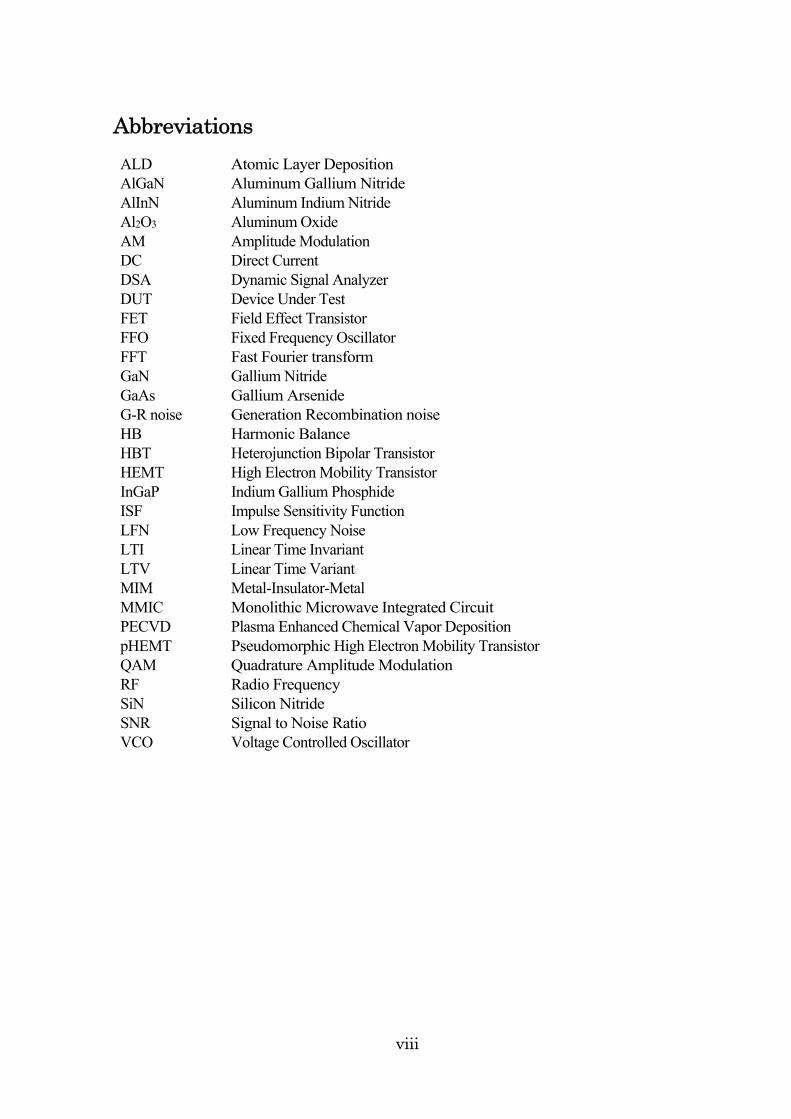
Abbreviations ALD AlGaN AlInN Al2O3
AM
Atomic Layer Deposition Aluminum Gallium Nitride Aluminum Indium Nitride Aluminum Oxide Amplitude Modulation
DC DSA
Direct Current Dynamic Signal Analyzer
DUT Device Under Test FET FFO
Field Effect Transistor Fixed Frequency Oscillator
FFT Fast Fourier transform GaN Gallium Nitride GaAs Gallium Arsenide G-R noise Generation Recombination noise HB Harmonic Balance HBT Heterojunction Bipolar Transistor HEMT High Electron Mobility Transistor InGaP Indium Gallium Phosphide ISF Impulse Sensitivity Function LFN Low Frequency Noise LTI Linear Time Invariant LTV MIM
Linear Time Variant Metal-Insulator-Metal
MMIC PECVD
Monolithic Microwave Integrated Circuit Plasma Enhanced Chemical Vapor Deposition
pHEMT QAM
Pseudomorphic High Electron Mobility Transistor Quadrature Amplitude Modulation
RF Radio Frequency SiN SNR
Silicon Nitride Signal to Noise Ratio
VCO Voltage Controlled Oscillator

ix

x
Contents
2.1 What is an oscillator? .................................................................................. 5
2.2 Phase noise ................................................................................................... 6
2.3 Noise sources ............................................................................................... 7
2.3.1 Thermal noise ..................................................................................... 7
2.3.2 Shot noise ............................................................................................ 8
2.3.3 Flicker noise (1/f noise) ...................................................................... 8
2.3.4 Generation-Recombination noise ..................................................... 9
2.4 Phase noise models ................................................................................... 10
2.4.1 Oscillator phase noise calculation .................................................. 10
2.4.2 Leeson’s phase noise model ............................................................ 11
2.4.3 Hajimiri’s phase noise model .......................................................... 12
2.5 Varactor ...................................................................................................... 15
3.1 Low frequency noise setup ....................................................................... 19
3.1.1 Current Amplifier based setup ....................................................... 19
3.1.2 Voltage Amplifier based setup ....................................................... 21
3.1.3 Setup Evaluation ............................................................................. 22
3.2 Benchmark of different transistor technologies .................................... 24
3.3 GaN HEMT Low Frequency Noise Studies ........................................... 28
3.3.1 Surface passivation and deposition methods ............................... 28

xi
3.3.2 Transistor gate length and source-drain distance ....................... 31
3.3.3 Transistor gate width ...................................................................... 33
4.1 A MMIC GaN HEMT fixed-frequency oscillator ................................... 36
4.1.1 Circuit design ................................................................................... 36
4.1.2 Measurement result ........................................................................ 36
4.2 A MMIC GaN HEMT Voltage-Controlled Oscillator ............................ 39
4.2.1 Circuit design ................................................................................... 39
4.2.2 Varactor characterization ............................................................... 40
4.2.3 VCO measurement result ............................................................... 41
4.3 Accurate phase noise simulation ............................................................. 44
1
Introduction Low phase noise oscillators are of paramount importance in modern wireless communication systems and radar systems. It has been shown that the phase noise of voltage-controlled-oscillator (VCO) in the systems using advanced modulation techniques, e.g. higher order Quadrature Amplitude Modulation (QAM), is one of the main limiting factors of system performance [1]. For the design of oscillators, low frequency noise (LFN) characterization is important since LFN is up-converted to phase noise around the microwave signal [2]. Although the exact origin of flicker noise is unclear, the level is known to differ between transistor technologies, e.g. the bipolar junction transistors (BJTs) have lower levels of flicker noise compared to field-effect transistor (FETs) [3]. On the one hand side, it is obvious that a device with low flicker noise level, e.g. a BJT, should be used for low phase noise oscillator design. On the other hand side, the phase noise is directly proportional to signal-to-noise ratio (SNR) [4] which favors devices that can deliver high power, e.g. GaN HEMT. Thus, there is a need to consider both noise and power when choosing transistor technology used for low phase noise oscillators.
It is known that the LFN level is related to the semiconductor lattice quality and device reliability [5-6]. The noise level is generally higher in a material with higher density of traps and defects. The impact of surface traps can be significantly reduced by good passivation methods. Some previous works have shown that a good passivation maintains a low gate leakage current and improves both DC and RF characteristics of the device [7-9]. Therefore, methods to improve LFN characteristic of a transistor, e.g. different passivation methods, are important to investigate for low phase noise oscillator design.
From the power handling capability perspective, GaN HEMT technology is a promising candidate for the design of low phase noise oscillators thanks to its particularly high breakdown voltage, enabling good SNR. An ideal GaN HEMT based VCO can theoretically reach very low phase noise, provided that its LFN level is not too high. However, none of the reported GaN HEMT VCOs

2
present performances near the theoretical limit [10-12] and in particular the performances reported are yet not comparable to other technologies such as GaAs-InGaP HBT [13-18], see Fig. 1-1. It should be mentioned that the phase noise theoretical limit of each transistor technology is calculated based on reasonable assumptions of available quality factor and power handling capability of each technology [19]. The major challenge is the relatively high level of flicker noise in GaN HEMTs, resulting in a phase noise slope that is steeper than -30 dB/decade. Thus, minimization of LFN up-conversion into phase noise is critical for the design of low phase noise oscillators based on GaN HEMT.
Recently, it has been demonstrated that fixed-frequency GaN HEMT oscillators can reach fairly low phase noise if the resonator impedance is well matched to the active device and the bias condition is carefully selected to avoid extensive flicker noise problems [20-23], see Fig. 1-1. It can be seen from those works that a typical good GaN HEMT based oscillator is often worse at near-carrier offsets, but better at far-carrier offsets compared to an InGaP HBT based oscillator. When the communication bandwidth increases, the far-carrier phase noise becomes more important and GaN HEMT based VCOs become more attractive since the flicker noise is not as critical as in narrower bandwidth systems. Besides, there is a demand for integration and GaN HEMT technology is excellent for other circuits, e.g. power amplifiers [24-25]. Therefore, GaN HEMT based oscillators are still of interest even though their near-carrier phase noise performance at this moment cannot be better than InGaP HBT based oscillators due to high flicker noise level.
Fig. 1-1 Phase noise at 100 kHz of published works in GaN HEMT and InGaP HBT technologies for MMIC oscillators, together with theoretical noise limits at 100 kHz of GaN HEMT and InGaP HBT technologies.

3
In this thesis, LFN of GaN HEMT devices are characterized and compared
to other transistor technologies (GaAs pHEMTs and GaAs InGaP HBTs). Besides, some factors which affect LFN of GaN HEMT devices (e.g. surface passivations, variations in transistor geometry) are studied. In addition, two MMIC oscillator designs with fairly good phase noise are also presented.
The thesis is arranged as follows. Chapter 2 gives general oscillator considerations such as oscillator phase noise, noise origins, phase noise models and figures of merit for varactors. Then, LFN characterization is discussed in detail in Chapter 3. Two different LFN setups are presented and evaluated in section 3.1. Section 3.2 compares LFN measurement of three different technologies InGaP HBT, GaAs pHEMT, and GaN HEMT. Then, the studies of GaN HEMT LFN are presented in section 3.3. Chapter 4 presents two MMIC oscillator designs: a 10 GHz fixed frequency oscillator (FFO) and a voltage controlled oscillator (VCO). Section 4.3 also demonstrates accurate phase noise simulations for the two designed oscillators. Finally, chapter 5 gives some conclusions and future works.

4
5
Fundamentals of phase noise in oscillators This chapter presents background of phase noise in oscillators. The definition of phase noise is introduced in section 2.2. Section 2.3 presents noise sources that influence an oscillator’s phase noise. Two types of phase noise models: the well-known Leeson and Hajimiri models, are described in section 2.4. Figures of merit of varactors are presented in section 2.5.
2.1 What is an oscillator?
An oscillator is an electronic circuit which can generate a periodic signal by converting DC power to RF power. The oscillator is one of the key building blocks in many digital electronic and RF communication systems. There are two commonly used methods for analysis of oscillators: the feedback oscillator and negative resistance oscillator approaches [26]. In the feedback method, the oscillator is considered as an amplifier with a positive feedback network as shown in Fig. 2-1. The amplifier and the feedback will form a loop and the condition for oscillation is that a part of output signal is combined in phase with the input signal and the amplitude of the loop gain is larger than unity, as expressed in (2-1) to (2-3).
,)()(
)()()(
sBsA
sAsVsV inout 1
(2-1)
,)()( 1sBsA (2-2)
,)()( 2nsBsA (2-3)
where A(s), B(s) are the gains and )(sA , )(sB are the phases of the amplifier and the feedback network, respectively.

6
Fig. 2-1 Block diagram of a feedback oscillator. Fig. 2-2 displays a block level schematic for a negative resistance oscillator.
It has a passive resonator separated from the amplifying active element. Each side is considered as a one-port network. Hence, the oscillation condition may be expressed by the reflection coefficients. The oscillation occurs when the one-port reflection coefficients of the two sides are in phase and their amplitudes’ product is greater than unity, as expressed in (2-4) to (2-5).
,)()( 1 ss AR (2-4)
,)()( 2nss AR (2-5)
where )(sR and )(sA are the reflection coefficients of the passive resonator and the amplifying active element, respectively.
Fig. 2-2 A block level schematic of a negative resistance oscillator.
2.2 Phase noise
An ideal output signal generated from an oscillator is a pure sinusoid at single frequency, see Fig. 2-3. It can be described in time domain as
,sin)( tfAtV 00 2 (2-6)
where 0A is the nominal amplitude and 0f is the nominal frequency.

7
In frequency domain, the ideal signal is shown as an impulse function at a single frequency. However, in practice, an electronic signal always has small random fluctuations in amplitude and phase which are known as amplitude noise and phase noise, see Fig. 2-3. Phase noise in frequency domain can be equivalently described by jitter in the time domain. A real signal including amplitude noise and phase noise can be expressed as
,)(sin)()( ttftAAtV nn 00 2 (2-7)
where An(t) is the amplitude noise and Фn(t) is phase noise.
The level of phase noise is often the factor that determines the performance of communication systems. Amplitude noise is less important since its effect is usually suppressed when the active device goes into compression.
Fig. 2-3 A sinusoidal signal generated from an oscillator in the ideal case and the
practical case (with amplitude noise and phase noise).
2.3 Noise sources
2.3.1 Thermal noise
Thermal noise is a type of electronic noise caused by the random thermal motion of the electrons [27]. It was formulated first by Johnson and Nyquist in 1926, and is often referred to as Johnson-Nyquist noise. Thermal noise is directly related to the absolute temperature T and is not affected by applied voltage or current. In a resistor, thermal noise is white Gaussian noise. Thermal noise can be modeled by a series voltage generator or shunt current generator as

8
,fkTRv 42 (2-8)
or ,fR
kTi 1
42 (2-9)
where k is Boltzmann’s constant, R is the circuit resistance, Δf is the bandwidth in hertz and T is the absolute temperature. At the room temperature (300oK), 20106614 .kT W s.
2.3.2 Shot noise
Unlike thermal noise, shot noise is always related to a direct current flow. It is present in diodes and bipolar transistors [27]. Shot noise is the result of the fluctuations in current which is caused by carriers travelling across the potential barrier at the junction. The noise current produced by shot noise can be modeled as:
,fqIi D 22 (2-10)
where q is the electronic charge ( 191061 .q C), ID is the bias current.
The shot noise is white noise and it is proportional to the bias current.
2.3.3 Flicker noise (1/f noise)
Flicker noise is a physical property in all active devices. It has a large impact on circuits, especially on oscillators. It is called 1/f noise since noise is generated with a slope inversely proportional to the frequency [3]. Flicker noise can be expressed in form of resistance noise spectrum (SR) or voltage noise spectrum (SV) or current noise spectrum (SI) or conductance noise spectrum (SG), and these spectra are usually normalized, e.g. SR/R2, SV/V2, SI/I2 or SG/G2. In 1969, Hooge proposed that the fluctuations in conductivity cause 1/f noise [28]. The conductivity fluctuations lead to changes in the resistance. Since the resistance varies with the carrier and mobility, changes in one of the two terms generate 1/f noise. This leads to two major 1/f noise models: one based on the fluctuations in carrier density and the other based on the mobility fluctuations [29]. Also in [28], an empirical relation was proposed by Hooge in which 1/f noise is inversely proportional to the number of carriers in the device.
,fNR
S HR
2
(2-11)
where N is the number of carriers in the device, f is the frequency and is the Hooge parameter.

9
According to Hooge, depends on the crystal quality and scattering mechanisms. He also proposed an average Hooge parameter of 2 10 and this value could be 2 or 3 orders of magnitude lower in perfect material. The Hooge parameter has been used as figure of merit for characterizing 1/f noise of many materials and devices [30-33]. However, most of LFN characterizations in open literature were often taken at low biasings which is not applicable for circuit applications. The author in [3] believes that Hooge parameter should be used only for material comparisons, not for device comparisons.
The exact origin of flicker noise is unclear. However, it is seen that 1/f noise is commonly associated with traps and defects in the device. The traps capture and release carriers randomly, leading to noise increase with energy concentrated at low frequencies [27]. Flicker noise is usually modeled as
,ff
IKi
fFE
AfDC
f 2 (2-12)
where Kf is level fitting, Af is the current dependency factor, and fFE is the frequency dependent power factor.
2.3.4 Generation-Recombination noise
Generation- Recombination (G-R) noise is a type of electrical noise generated by fluctuations in the number of free carriers in semiconductor materials [34]. It is related to the random transitions of carriers between states in different energy bands, e.g. between conduction band and trap levels in the bandgap, conduction and valence bands [34]. G-R noise has Lorentzian power spectral density which is expressed as [28]
,)(
222
2
222 1
4
N
N
N
S
G
S
R
S NGR (2-13)
where τ is a relaxation time which is a characteristic of the trap, is the
angular frequency, 22 NN /)( is the fluctuation quantity.
G-R type of noise current can be modeled as
,f
f
f
IKi
b
AbDC
b
2
2
1
(2-14)
where Kb and Ab are fitting parameters, fb is the frequency when G-R centers are activated.

10
Flicker noise and G-R noise are two dominant noise sources at low
frequencies. In general, the noise sources in Field-Effect-Transistor (FET) and Bipolar Junction Transistor (BJT) are different. In FETs, the thermal noise is caused by the gate and drain resistances while the flicker noise and G-R noise appear in the channel. The shot noise in FET devices is generally low and can be neglected. In BJTs, the base resistance causes the thermal noise while the shot noise appears at the base-emitter junction and the collector-base junction. There is both flicker noise and G-R noise in BJTs but the level of flicker noise is much lower in BJTs compared to FETs.
2.4 Phase noise models
As already mentioned above, phase noise is an important parameter in the performance of a system. In an oscillator, low frequency noise (flicker noise and G-R noise) is up-converted into phase noise around the microwave signal. A phase noise model has to take into account the effect of low frequency noise. This section presents two different phase noise models: Leeson’s model and Hajimiri’s model. The former is a linear time invariant (LTI) model while the latter is linear time variant (LTV) model.
2.4.1 Oscillator phase noise calculation
Assuming that we have a perfect RLC oscillator composed of a lossy resonator and a noiseless energy restorer as seen in Fig. 2-4 [35]. The noiseless restoration box would supply energy to the RLC tank in order to compensate for losses in the resistance R.
Fig. 2-4 A perfect RLC oscillator In this model, the tank resistance is the only noisy element. Assuming that
the resistor has only thermal noise, the single sideband phase noise in 1/f2 region, see Fig. 2-5(a), is expressed as [36]

11
,log
2
010 22
110
fQ
f
P
kTf
sig
L (2-15)
where 0f is the output frequency, Δf is the offset from the output frequency, k is
Boltzmann’s constant, Q is the unloaded quality factor of the tank ( LRQ 0/ ),
Psig is the power stored in the resonator.
(a) (b)
Fig. 2-5 (a) Phase noise in 1/f2 region. (b) Experimental spectrum
Equation (2-15) is modified in order to fit the experimental spectrum, as shown in (2-16) and Fig. 2-5(b).
.log
2
010 2
12
110
fQ
f
P
kTf
sig
L (2-16)
2.4.2 Leeson’s phase noise model
Leeson’s model is probably the most well-known phase noise model which was proposed by D. B. Leeson in 1966 [4].
The phase noise described in (2-16) is the case when only thermal noise is considered. In reality, the active device is also affected by flicker noise. When both thermal noise and phase noise are included, the single sideband phase noise is expressed as in (2-17).
,log /
f
f
fQ
f
P
FkTf f
Lsig
31
2
010 1
21
210L (2-17)
where 0f is the output frequency, Δf is the offset from the output frequency, F is
an effective noise factor, k is Boltzmann’s constant, QL is the loaded quality factor, Psig is the power stored in the resonator, and Δf1/f3 is the 1/f3 corner frequency.
Depending on the loaded QL-factor and low frequency noise corner frequency
Δf1/f3, two possible cases may occur when LFN is up-converted into phase noise as described by Leeson’s equation, see Figs. 2-6 (a) and (b).
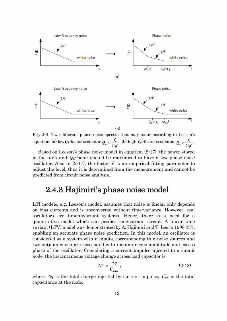
12
(a)
(b)
Fig. 2-6 Two different phase noise spectra that may occur according to Leeson’s
equation. (a) lowQL-factor oscillator,f
fQL
2
0 . (b) high QL-factor oscillator, f
fQL
2
0 .
Based on Leeson’s phase noise model in equation (2-17), the power stored in the tank and QL-factor should be maximized to have a low phase noise oscillator. Also in (2-17), the factor F is an empirical fitting parameter to adjust the level, thus it is determined from the measurement and cannot be predicted from circuit noise analysis.
2.4.3 Hajimiri’s phase noise model
LTI models, e.g. Leeson’s model, assumes that noise is linear, only depends on bias currents and is upconverted without time-variance. However, real oscillators are time-invariant systems. Hence, there is a need for a quantitative model which can predict time-variant circuit. A linear time variant (LTV) model was demonstrated by A. Hajimiri and T. Lee in 1998 [37], enabling an accurate phase noise prediction. In this model, an oscillator is considered as a system with n inputs, corresponding to n noise sources and two outputs which are associated with instantaneous amplitude and excess phase of the oscillator. Considering a current impulse injected to a circuit node, the instantaneous voltage change across load capacitor is
,totalC
qV
(2-18)
where Δq is the total charge injected by current impulse, Ctot is the total capacitance at the node.

13
The change in phase is proportional to the change in voltage. The amount of excess phase is also proportional to the ratio of injected charge to the maximum charge swing across the capacitor [37]. Thus, it can be expressed as
,)()(maxmax q
qt
V
Vt
00 (2-19)
where Vmax is the peak amplitude of the oscillator, qmax is maximum charge displacement and )( t0 is referred to as impulse sensitivity function (ISF).
Based on the ISF, the unit impulse response for excess phase can be expressed as
),(),(
max
tuq
th 0 (2-20)
where u(t) is the unit step, τ is the time when impulse is injected. A maximum phase change occurs when an impulse is injected at the zero
crossing without the change in the amplitude. On the contrary, an impulse injected at the peak voltage causes maximum voltage change, but does not cause phase change. Thus, the ISF is a periodic function with the same periodicity as the signal waveform. It can be expressed by a Fourier expansion as
),cos()(
1
00
0 2 nnn tnc
c (2-21)
where cn are real-valued coefficients and θn is the phase of nth harmonic. The ISF can be calculated from oscillation waveforms obtained from circuit simulation, e.g. from a circuit simulation algorithm. Then, the excess phase may be determined by a superposition integral
,)()()(),()(max
t
ditq
ditht 0
1 (2-22)
where i(t) is the input noise current injected at the node of interest.
Substituting equation (2-21) into (2-22), the excess phase noise is obtained as
.)()()()(max
t
n
t
n ditcdic
qt
10
0
2
1 (2-23)
Based on equation (2-23), it can be seen that noise at DC is up-converted to phase noise around the microwave signal 0 .

14
If only thermal noise is considered, the phase noise can be expressed [37]
),log(log)(maxmax
2
2
2
2
220
22
210
410
fi
cfinrmsn
nn
L (2-24)
with 222
00
2 21
rmsn
n dxxc
)( where Γrms is the rms value of Γ(x).
For flicker noise up-conversion, only the DC coefficient is relevant, thus the noise spectrum can be calculated as [37]
),log()log()( /
max
/
max
fnfnn fi
q
cfi
q
c1
2
2
2
20
2
21
20
2
810
410L (2-25)
where c0 is the dc value of the ISF.
In Hajimiri’s theory, he proved that the 1/f3 corner frequency is not the same as the device 1/f corner. Their relation is proven to be as [37]
.///
2
1
012
20
11 23
c
ccf
rmsff
(2-26)
It should be noted that the noise sources in the oscillator might be time variant with the same period as the oscillation, e.g. current dependent noise which is known as cyclostationary noise sources. Noise sources without time-variance are referred to as stationary noise sources, e.g. thermal noise. A cyclostationary noise source can be expressed by stationary noise )(tin0
multiplied to the normalized periodic noise amplitude modulation function)( t0 .
).()()( ttiti nn 00 (2-27)
A new effective ISF is defined with the cyclostationary noise source as
).()()( ttteff 000 (2-28)
This effective ISF is used for accurate phase noise calculation in 1/f2 and 1/f3 regions based on (2-24) and (2-25), respectively.
In short, Hajimiri’s model is based on the periodic function ISF to analyze the oscillator phase noise. In this model, the cyclostationary noise source which strongly depends on the signal waveform of the oscillator is also introduced.
15
2.5 Varactor
In oscillator design, the frequency of output signal can be fixed or variable. For microwave applications, the design of a fixed frequency oscillator is usually based on the resonant inductor (L) and capacitor (C) circuits which can be in series or in parallel. In the microwave monolithic integrated circuit (MMIC) technology, inductors are usually implemented as spiraled transmission lines and capacitors as metal-insulator-metal (MIM) capacitors. In order to tune the oscillation frequency, the variable elements, e.g. variable inductor or variable capacitor (varactor) are used. In MMIC, a varactor diode is commonly used to replace for MIM capacitors, enabling the tuning of the oscillation frequency. The varactor uses p-n junction in the reverse bias region and its capacitance is varied with a reverse applied voltage. The C-V relationship is
,)(
)(
0
0
1
1
m
mj VCVC (2-29)
where 0C is zero bias capacitance, 0 is the built-in potential of p-n junction,
the exponent η is a factor depending on how the doping density of the semiconductors depend on distance away from the junction, Vm is the applied voltage.
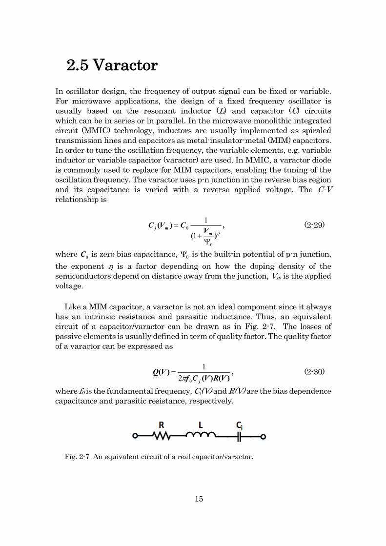
Like a MIM capacitor, a varactor is not an ideal component since it always has an intrinsic resistance and parasitic inductance. Thus, an equivalent circuit of a capacitor/varactor can be drawn as in Fig. 2-7. The losses of passive elements is usually defined in term of quality factor. The quality factor of a varactor can be expressed as
,)()(
)(VRVCf
VQj02
1
(2-30)
where f0 is the fundamental frequency, Cj(V) and R(V) are the bias dependence capacitance and parasitic resistance, respectively.
Fig. 2-7 An equivalent circuit of a real capacitor/varactor.

16
In general, the Q-factor of a varactor is lower than for a MIM capacitor. An
oscillator design based on varactor is called a voltage-controlled-oscillator (VCO). The oscillation frequency of a VCO is expressed as
.)( mj VLC
f2
10 (2-31)
The tuning range of a VCO is associated with the ratio Cmax/Cmin of the
varactor. Moreover, it also depends on the inclusion-factor of the varactor in the tank. A high inclusion factor will help to increase the tuning range.
In practice, the Q-factor characterization of a varactor is quite sensitive to
measurement errors since it relies on the accuracy of the extracted parasitic resistance. An alternative method that is based on a resonant structure was proposed by Deloach in 1964 [38]. A Deloach structure is a through transmission line shunted with a series resonant circuit consisting of a microstrip line and a varactor connected in series to ground, as shown in Fig. 2-8.
Z0 Z0Port 1 Port 2
Varactor
Microstrip line
Fig. 2-8 Schematic diagram of a Deloach test structure.
17
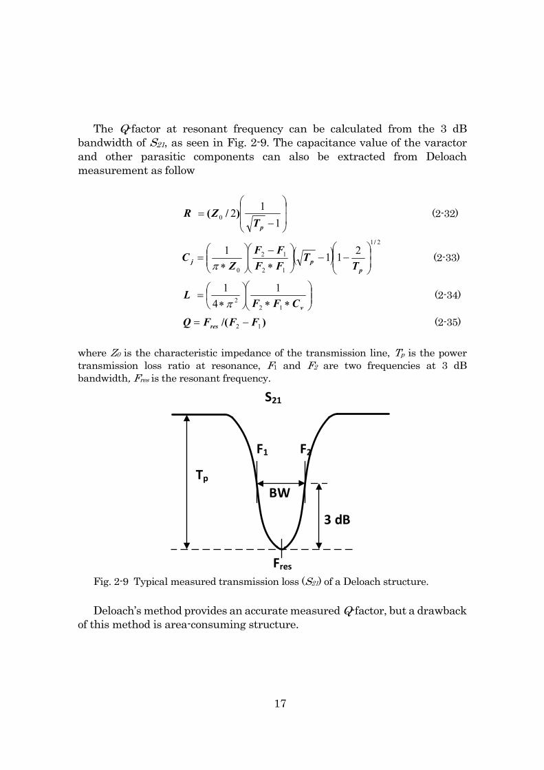
The Q-factor at resonant frequency can be calculated from the 3 dB bandwidth of S21, as seen in Fig. 2-9. The capacitance value of the varactor and other parasitic components can also be extracted from Deloach measurement as follow
1
120
pTZR )/( (2-32)
21
12
12
0
211
1/
p
pj TT
FF
FF
ZC
(2-33)
vCFFL
122
1
4
1
(2-34)
)/( 12 FFFQ res (2-35)
where Z0 is the characteristic impedance of the transmission line, Tp is the power transmission loss ratio at resonance, F1 and F2 are two frequencies at 3 dB bandwidth, Fres is the resonant frequency.
Tp
F1 F2
3 dB
BW
Fres
S21
Fig. 2-9 Typical measured transmission loss (S21) of a Deloach structure. Deloach’s method provides an accurate measured Q-factor, but a drawback
of this method is area-consuming structure.

18
19
Low Frequency Noise Characterization This chapter presents details on LFN characterization. Two types of LFN setup used for the LFN measurement are described in section 3.1, and followed by setup verification. In section 3.2, GaN HEMT LFN is benchmarked versus other transistor technologies such as GaAs pHEMT, GaAs InGaP HBT for low phase noise applications. Section 3.3 investigates the effects of different passivations and deposition methods and the variations of transistor geometry on the LFN for two types of GaN based HEMTs: AlGaN/GaN based HEMTs and AlInN/GaN based HEMTs.
3.1 Low frequency noise setup
The principle in LFN measurement is that the device is biased in operating condition and the noise spectra detected in a signal analyzer. Beside the signal analyzer, a low-noise baseband amplifier is needed. It is possible to use either current or voltage amplifiers. One of the main challenges in the setup is the low-frequency bias Tees used to separate the noise from the DC signal. This chapter presents two different LFN measurement set-ups based on a current amplifier and voltage amplifier, respectively.
3.1.1 Current Amplifier based setup
This LFN measurement setup, called setup A, was proposed by Franz Sischka from Agilent Technologies [39]. The setup is based on a current to voltage preamplifier from Stanford Research (SR570) as seen in Fig. 3-1 and its internal supply for collector current/drain voltage biasing. The base
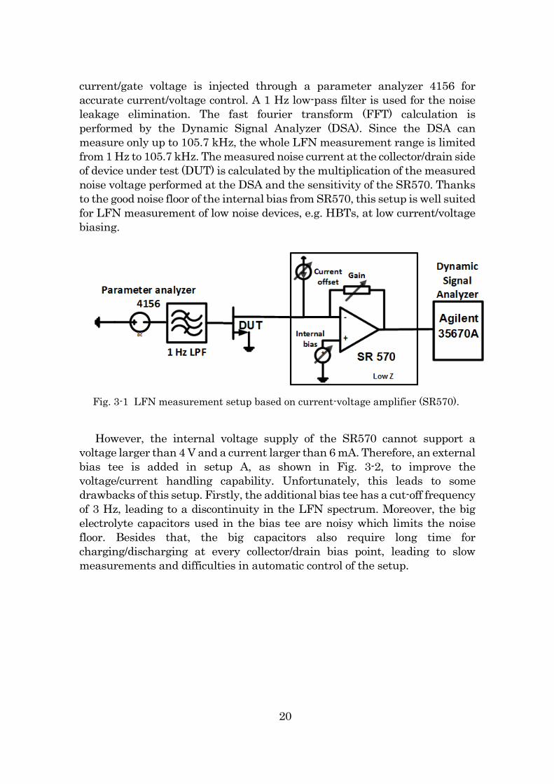
20
current/gate voltage is injected through a parameter analyzer 4156 for accurate current/voltage control. A 1 Hz low-pass filter is used for the noise leakage elimination. The fast fourier transform (FFT) calculation is performed by the Dynamic Signal Analyzer (DSA). Since the DSA can measure only up to 105.7 kHz, the whole LFN measurement range is limited from 1 Hz to 105.7 kHz. The measured noise current at the collector/drain side of device under test (DUT) is calculated by the multiplication of the measured noise voltage performed at the DSA and the sensitivity of the SR570. Thanks to the good noise floor of the internal bias from SR570, this setup is well suited for LFN measurement of low noise devices, e.g. HBTs, at low current/voltage biasing.
Fig. 3-1 LFN measurement setup based on current-voltage amplifier (SR570).
However, the internal voltage supply of the SR570 cannot support a voltage larger than 4 V and a current larger than 6 mA. Therefore, an external bias tee is added in setup A, as shown in Fig. 3-2, to improve the voltage/current handling capability. Unfortunately, this leads to some drawbacks of this setup. Firstly, the additional bias tee has a cut-off frequency of 3 Hz, leading to a discontinuity in the LFN spectrum. Moreover, the big electrolyte capacitors used in the bias tee are noisy which limits the noise floor. Besides that, the big capacitors also require long time for charging/discharging at every collector/drain bias point, leading to slow measurements and difficulties in automatic control of the setup.
21
Fig. 3-2 Setup A with external bias tee.
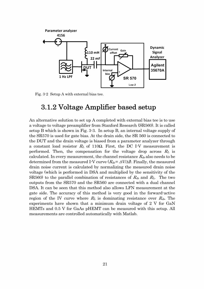
3.1.2 Voltage Amplifier based setup
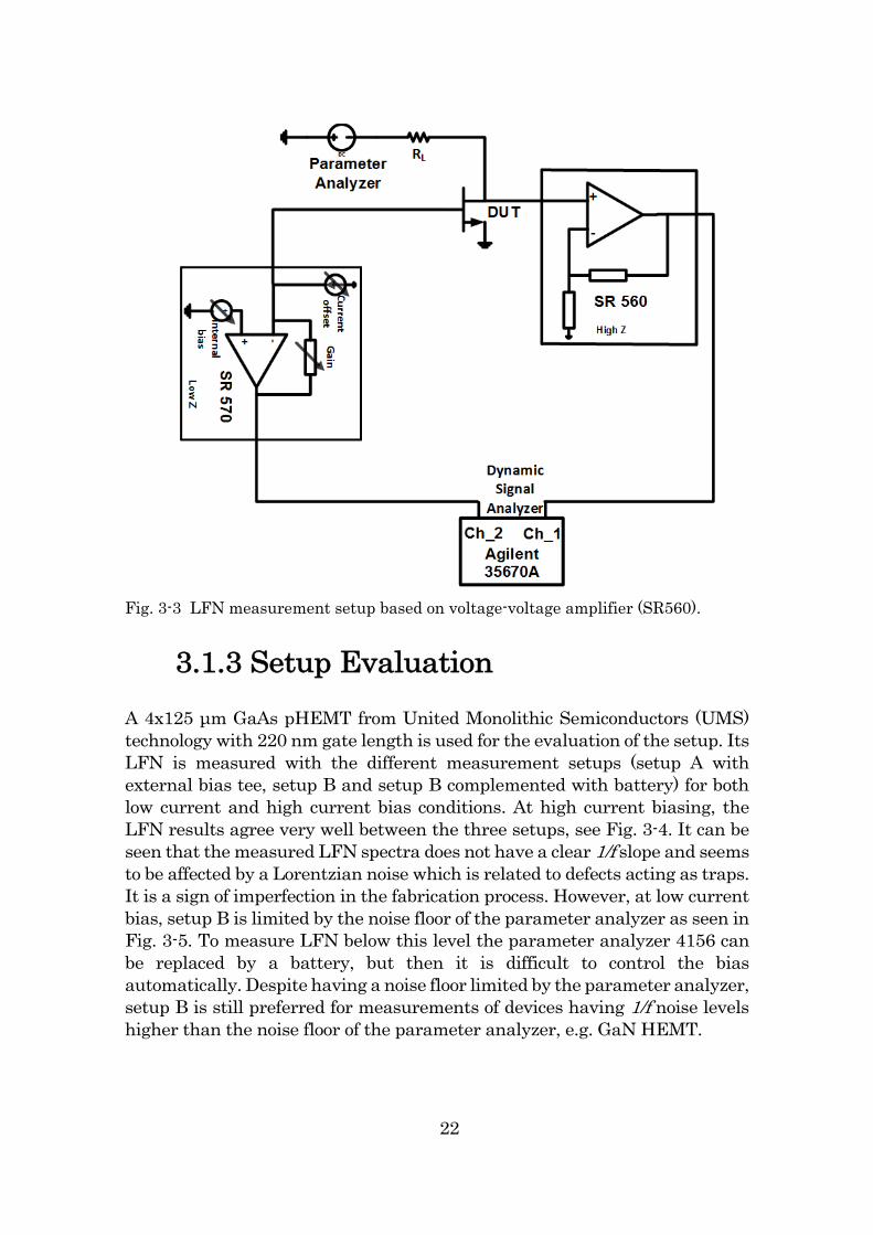
An alternative solution to set up A completed with external bias tee is to use a voltage to voltage preamplifier from Stanford Research (SR560). It is called setup B which is shown in Fig. 3-3. In setup B, an internal voltage supply of the SR570 is used for gate bias. At the drain side, the SR 560 is connected to the DUT and the drain voltage is biased from a parameter analyzer through a constant load resistor RL of 110Ω. First, the DC I-V measurement is performed. Then, the compensation for the voltage drop across RL is calculated. In every measurement, the channel resistance Rds also needs to be determined from the measured I-V curve (Rds = ∆V/∆I). Finally, the measured drain noise current is calculated by normalizing the measured drain noise voltage (which is performed in DSA and multiplied by the sensitivity of the SR560) to the parallel combination of resistances of Rds and RL. The two outputs from the SR570 and the SR560 are connected with a dual channel DSA. It can be seen that this method also allows LFN measurement at the gate side. The accuracy of this method is very good in the forward-active region of the IV curve where RL is dominating resistance over Rds. The experiments have shown that a minimum drain voltage of 2 V for GaN HEMTs and 0.5 V for GaAs pHEMT can be measured with this setup. All measurements are controlled automatically with Matlab.
22
Fig. 3-3 LFN measurement setup based on voltage-voltage amplifier (SR560).
3.1.3 Setup Evaluation
A 4x125 μm GaAs pHEMT from United Monolithic Semiconductors (UMS) technology with 220 nm gate length is used for the evaluation of the setup. Its LFN is measured with the different measurement setups (setup A with external bias tee, setup B and setup B complemented with battery) for both low current and high current bias conditions. At high current biasing, the LFN results agree very well between the three setups, see Fig. 3-4. It can be seen that the measured LFN spectra does not have a clear 1/f slope and seems to be affected by a Lorentzian noise which is related to defects acting as traps. It is a sign of imperfection in the fabrication process. However, at low current bias, setup B is limited by the noise floor of the parameter analyzer as seen in Fig. 3-5. To measure LFN below this level the parameter analyzer 4156 can be replaced by a battery, but then it is difficult to control the bias automatically. Despite having a noise floor limited by the parameter analyzer, setup B is still preferred for measurements of devices having 1/f noise levels higher than the noise floor of the parameter analyzer, e.g. GaN HEMT.

23
Fig.3-4 Measured LFN spectra of 4x125 μm pHEMT device versus the frequency for different measurement methods at Vd = 3 V, Vg = -0.8 V and Id = 16 mA.
Fig.3-5 Measured LFN spectra of 4x125 μm pHEMT device versus the frequency for different measurement methods at Vd = 3 V, Vg = -1.2 V and Id = 0.04 mA.
24
3.2 Benchmark of different transistor technologies
In this part, the LFN of some commonly used MMIC transistor technologies, e.g., GaAs-InGaP HBT, GaAs pHEMT and GaN HEMT are presented. GaAs InGaP HBTs require a low noise floor; they are measured with setup A, while GaAs pHEMT and GaN HEMTs are measured with setup B.
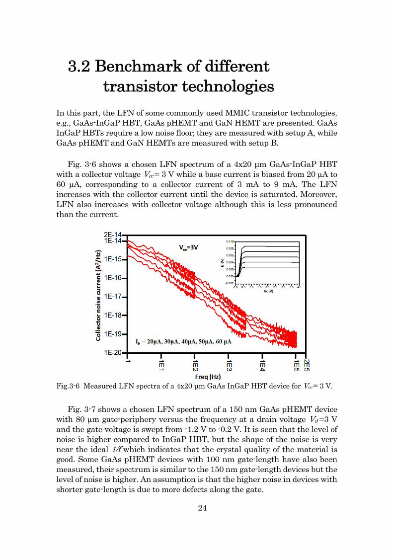
Fig. 3-6 shows a chosen LFN spectrum of a 4x20 μm GaAs-InGaP HBT with a collector voltage Vcc = 3 V while a base current is biased from 20 µA to 60 µA, corresponding to a collector current of 3 mA to 9 mA. The LFN increases with the collector current until the device is saturated. Moreover, LFN also increases with collector voltage although this is less pronounced than the current.
Fig.3-6 Measured LFN spectra of a 4x20 μm GaAs InGaP HBT device for Vcc = 3 V.
Fig. 3-7 shows a chosen LFN spectrum of a 150 nm GaAs pHEMT device
with 80 µm gate-periphery versus the frequency at a drain voltage Vd =3 V and the gate voltage is swept from -1.2 V to -0.2 V. It is seen that the level of noise is higher compared to InGaP HBT, but the shape of the noise is very near the ideal 1/f which indicates that the crystal quality of the material is good. Some GaAs pHEMT devices with 100 nm gate-length have also been measured, their spectrum is similar to the 150 nm gate-length devices but the level of noise is higher. An assumption is that the higher noise in devices with shorter gate-length is due to more defects along the gate.

25
Fig.3-7 Measured LFN spectra of a 4x20μm pHEMT with 150nm gate length for Vd =3 V.
Several GaN HEMT devices from different vendors have also been
measured. These devices all have different gate widths and number of fingers. The drain voltages are held constant at 2 V, 6 V and 10 V while the gate bias is swept. Fig. 3-8 shows a typical LFN spectrum of a 2x75 μm GaN HEMT with 250 nm gate length at 10 V drain voltage. It is observed that the slope is somewhat steeper than 1/f. It can be expressed as 1/fγ. Some previous works have shown that the slope of GaN HEMT, ɣ ,varies from 1 to 1.3 [3]. However, in this experiment the slope is even steeper, from 1.3 to 1.5. The whole LFN data from several different measured devices are summarized in Table I. It should be mentioned that the measurements listed in Table I are taken in the forward active region, where the flicker noise normalized versus power has its lowest value.

26
Fig.3-8 Measured LFN spectra of a 2x75 μm GaN HEMT with 250 nm gate length, for Vd =10 V.
The measured LFN of different devices verify the well-known fact that bipolar devices have lower flicker noise compared to field-effect-transistors. However, since the measurements of different devices are taken for quite different bias points, the measured noise level should be normalized versus power to have a fair comparison. With the target on oscillator applications, we may initiate from Leeson’s equation in which the oscillator’s single-side-band phase noise spectrum is defined as (2-17). It is seen that oscillator phase noise is proportional to (LFN)/Psig. Assuming a well-designed oscillator and a constant conversion efficiency, a fair benchmark is LFN/Pdc, where Pdc=Vd*Id. Table I shows that the LFN of GaN HEMT technology is about the same level as for GaAs pHEMT, but when normalized to DC power, GaN HEMT has a better performance compared to GaAs pHEMT. For example, at 10 kHz the best GaN HEMT device demonstrates a benchmark parameter approximately five times better than the best GaAs pHEMT one, corresponding to a predicted improvement of 7 dB in oscillator phase noise. The best performance in terms of absolute flicker noise levels is obtained for GaAs-InGaP HBTs. However, for higher frequencies the difference is less, and in particular the power normalized noise spectra of GaN HEMT is rather competitive at high frequencies. For example, at 100 kHz, the best GaN HEMT device has power normalized to flicker noise that is better than the measured InGaP HBTs.

27
TA
BL
E I
CO
MP
AR
ISO
N O
F B
EN
CH
MA
RK
PA
RA
ME
TE
RS
OF
DIF
FE
RE
NT
DE
VIC
ES
28
3.3 GaN HEMT Low Frequency Noise Studies
As shown in section 3.2, GaN HEMT is a promising candidate for low phase noise oscillators design. Thus, an in-depth study of some factors which affect LFN characteristics of GaN HEMT devices is performed in this section. The LFN measurements of the devices in this part are carried out with setup B as described in section 3.1.
3.3.1 Surface passivation and deposition methods
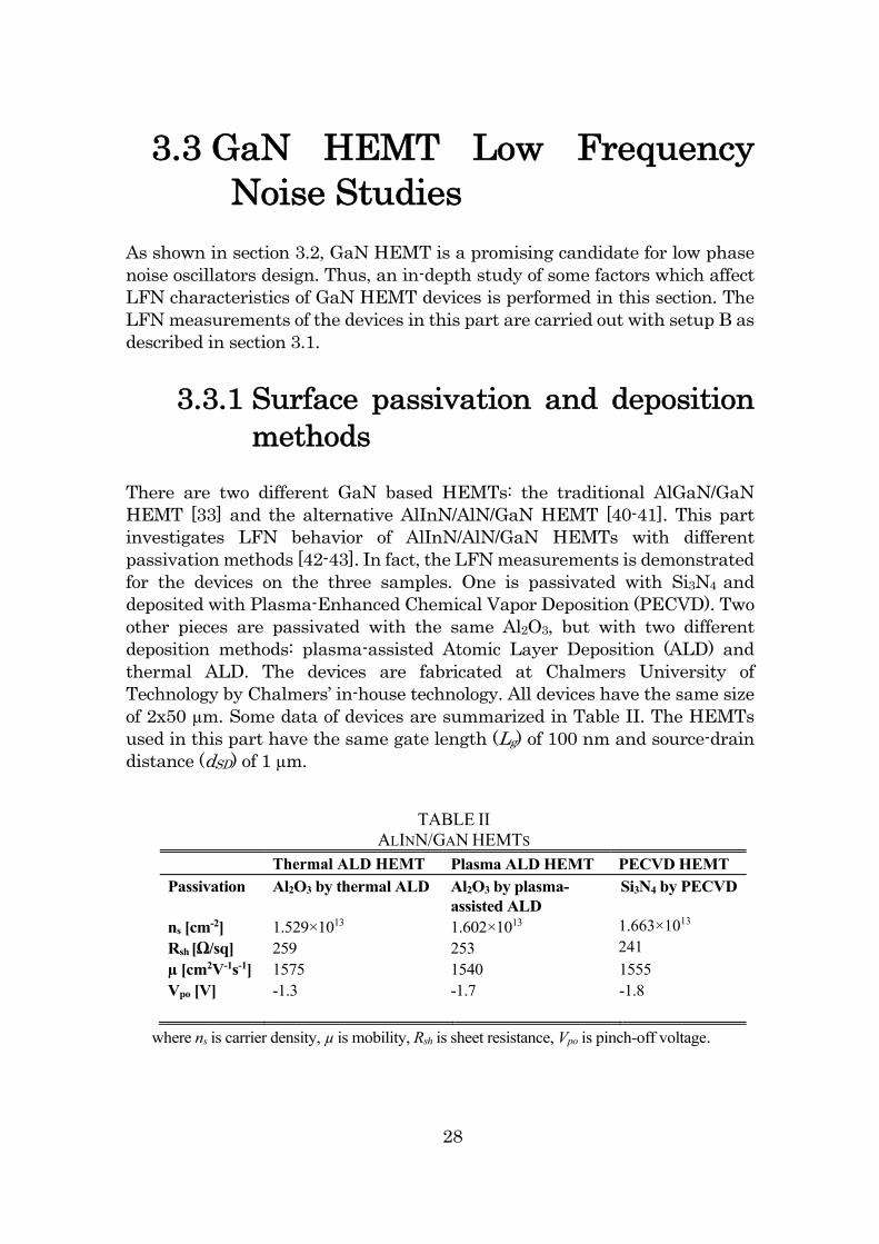
There are two different GaN based HEMTs: the traditional AlGaN/GaN HEMT [33] and the alternative AlInN/AlN/GaN HEMT [40-41]. This part investigates LFN behavior of AlInN/AlN/GaN HEMTs with different passivation methods [42-43]. In fact, the LFN measurements is demonstrated for the devices on the three samples. One is passivated with Si3N4 and deposited with Plasma-Enhanced Chemical Vapor Deposition (PECVD). Two other pieces are passivated with the same Al2O3, but with two different deposition methods: plasma-assisted Atomic Layer Deposition (ALD) and thermal ALD. The devices are fabricated at Chalmers University of Technology by Chalmers’ in-house technology. All devices have the same size of 2x50 µm. Some data of devices are summarized in Table II. The HEMTs used in this part have the same gate length (Lg) of 100 nm and source-drain distance (dSD) of 1 µm.
TABLE II ALINN/GAN HEMTS
Thermal ALD HEMT Plasma ALD HEMT PECVD HEMT Passivation Al2O3 by thermal ALD Al2O3 by plasma-
assisted ALD Si3N4 by PECVD
ns [cm-2] 1.529×10¹³ 1.602×10¹³ 1.663×10¹³
Rsh [Ω/sq] 259 253 241
µ [cm2V-1s-1] 1575 1540 1555 Vpo [V] -1.3 -1.7 -1.8
where ns is carrier density, µ is mobility, Rsh is sheet resistance, Vpo is pinch-off voltage.

29
In this study, LFN is measured under high drain voltage condition which is relevant for oscillator applications. The drain voltage is held at 10 V while the gate bias is swept. The measured drain noise current spectral density SI (A2/Hz) normalized to the drain current squared (I2) is used as LFN figure of merit.
Fig. 3-9 Drain noise current spectra of the three AlInN/AlN/GaN HEMTs versus frequency at Vdd = 10 V, Idd 17 mA.
Fig. 3-9 shows the normalized drain current noise spectra (SI/I2) of the
three AlInN/AlN/GaN HEMTs at a bias of Vdd = 10 V and Idd 17 mA. This is a reasonable operating point of an oscillator circuit. It can be seen that the noise spectrum level of the sample passivated with Al2O3 by thermal ALD is significantly lower than for the two other samples. Furthermore, the noise spectrum of the thermally deposited Al2O3 HEMT has a nearly constant slope 1/fγ with ɣ=1.3 while the noise spectra of the plasma deposited Al2O3 and PECVD deposited Si3N4 HEMTs are more Lorentzian type, which indicates the existence of deep level traps [30].
Fig. 3-10 shows the LFN spectral densities at the 10 kHz off-set versus DC drain current measured at Vdd=10 V of the three HEMTs in this study, a commercial AlGaN/GaN HEMT measured in section 3.2 and a state-of-the-art AlGaN/GaN HEMT published in [3]. There is no significant difference in noise performance between the three AlInN/AlN/GaN HEMTs for low drain currents while for larger drain currents, the thermal ALD Al2O3 HEMT presents an order of magnitude lower noise compared to the plasma ALD Al2O3 HEMT and about 50 times better noise compared to the PECVD Si3N4
HEMT. For an oscillator circuit, the difference in LFN between thermal ALD HEMT and the two other HEMTs would manifest more than 10 dB
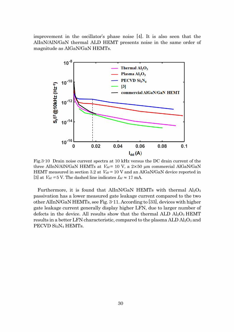
30
improvement in the oscillator’s phase noise [4]. It is also seen that the AlInN/AlN/GaN thermal ALD HEMT presents noise in the same order of magnitude as AlGaN/GaN HEMTs.
Fig.3-10 Drain noise current spectra at 10 kHz versus the DC drain current of the three AlInN/AlN/GaN HEMTs at Vdd = 10 V, a 2 50 µm commercial AlGaN/GaN HEMT measured in section 3.2 at Vdd = 10 V and an AlGaN/GaN device reported in [3] at Vdd = 5 V. The dashed line indicates Idd 17 mA.
Furthermore, it is found that AlInN/GaN HEMTs with thermal Al2O3 passivation has a lower measured gate leakage current compared to the two other AlInN/GaN HEMTs, see Fig. 3-11. According to [33], devices with higher gate leakage current generally display higher LFN, due to larger number of defects in the device. All results show that the thermal ALD Al2O3 HEMT results in a better LFN characteristic, compared to the plasma ALD Al2O3 and PECVD Si3N4 HEMTs.

31
Fig. 3-11 Measured gate leakage current of the three AlInN/AlN/GaN HEMTs versus the effective gate bias Vgn (Vdd = 10V). The dashed line corresponds to Idd 17 mA.
The large signal microwave properties of the three different passivations have also been characterized with 3 GHz load-pull measurements [43]. The output power densities of the thermal ALD Al2O3, plasma ALD Al2O3, and PECVD HEMTs Si3N4 are 1.9, 3.3, and 2.4 W/mm, respectively. Interestingly, the maximum power density is not obtained for the same passivation as the lowest flicker noise. It means there is a trade-off between LFN result and load-pull measurement result. Nevertheless, for oscillator applications, the thermal ALD HEMT is much more suitable due to its significantly lower flicker noise level. Assuming flicker noise as the dominant noise source, the 10-50 times improvement in noise spectral density would result in more than 10 dB improvement in oscillator phase noise while the difference in power density between the three samples would affect phase noise by less than 3 dB [4].
3.3.2 Transistor gate length and source-drain distance
In this part, LFN measurements of AlInN/AlN/GaN HEMTs with variation in the gate length (Lg) and the source-drain distance (dSD) are presented. The study is based on samples passivated with Al2O3 plasma-assisted ALD mentioned in Section 3.2.1. The measured devices have the same gate width (2x50 µm), but differ in Lg and dSD. Three different gate lengths (Lg = 50, 100, 180 nm) and three different source-drain distance (dSD = 1, 1.5 and 2 µm) are investigated.
32
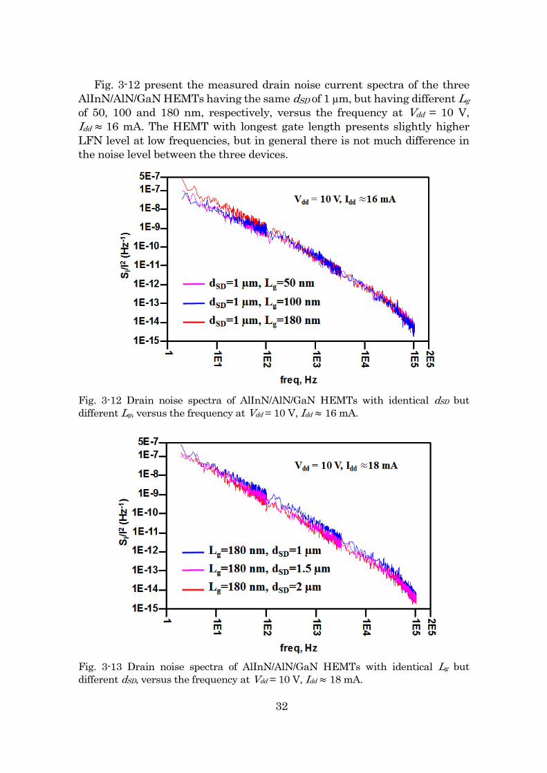
Fig. 3-12 present the measured drain noise current spectra of the three AlInN/AlN/GaN HEMTs having the same dSD of 1 µm, but having different Lg
of 50, 100 and 180 nm, respectively, versus the frequency at Vdd = 10 V, Idd 16 mA. The HEMT with longest gate length presents slightly higher LFN level at low frequencies, but in general there is not much difference in the noise level between the three devices.
Fig. 3-12 Drain noise spectra of AlInN/AlN/GaN HEMTs with identical dSD but different Lg, versus the frequency at Vdd = 10 V, Idd 16 mA.
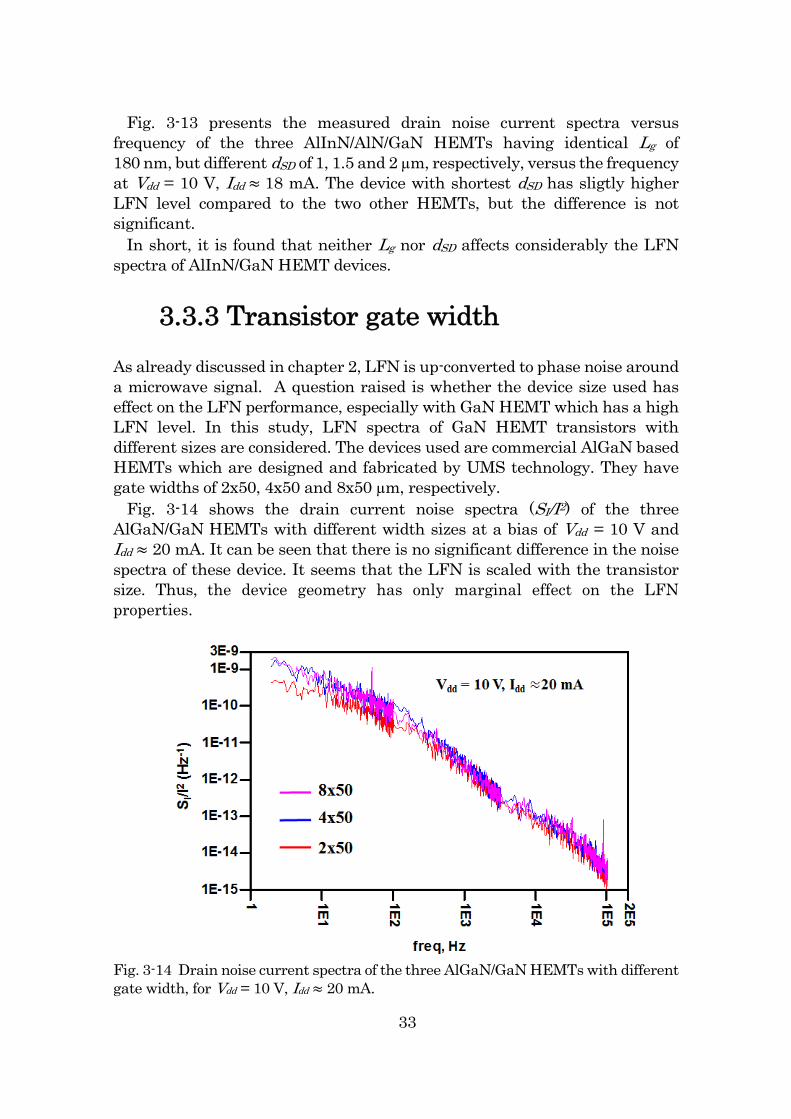
Fig. 3-13 Drain noise spectra of AlInN/AlN/GaN HEMTs with identical Lg but different dSD, versus the frequency at Vdd = 10 V, Idd 18 mA.
33
Fig. 3-13 presents the measured drain noise current spectra versus frequency of the three AlInN/AlN/GaN HEMTs having identical Lg of 180 nm, but different dSD of 1, 1.5 and 2 µm, respectively, versus the frequency at Vdd = 10 V, Idd 18 mA. The device with shortest dSD has sligtly higher LFN level compared to the two other HEMTs, but the difference is not significant.
In short, it is found that neither Lg nor dSD affects considerably the LFN spectra of AlInN/GaN HEMT devices.
3.3.3 Transistor gate width
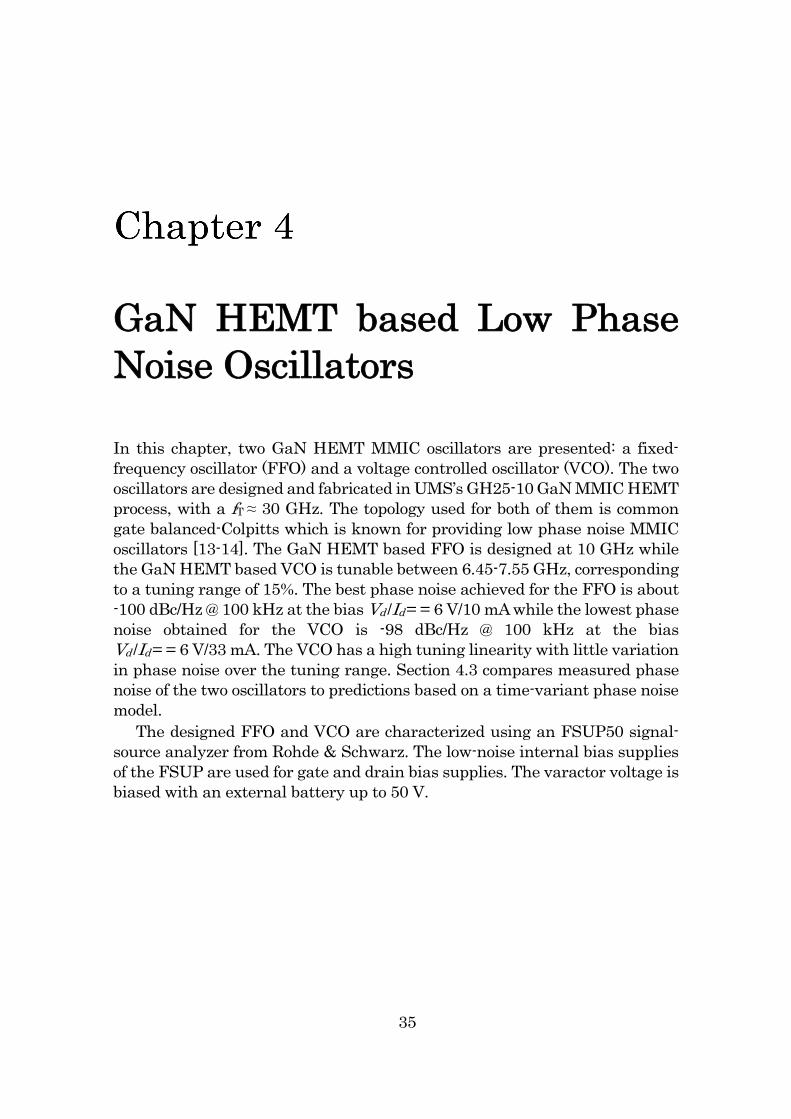
As already discussed in chapter 2, LFN is up-converted to phase noise around a microwave signal. A question raised is whether the device size used has effect on the LFN performance, especially with GaN HEMT which has a high LFN level. In this study, LFN spectra of GaN HEMT transistors with different sizes are considered. The devices used are commercial AlGaN based HEMTs which are designed and fabricated by UMS technology. They have gate widths of 2x50, 4x50 and 8x50 µm, respectively.
Fig. 3-14 shows the drain current noise spectra (SI/I2) of the three AlGaN/GaN HEMTs with different width sizes at a bias of Vdd = 10 V and Idd 20 mA. It can be seen that there is no significant difference in the noise spectra of these device. It seems that the LFN is scaled with the transistor size. Thus, the device geometry has only marginal effect on the LFN properties.
Fig. 3-14 Drain noise current spectra of the three AlGaN/GaN HEMTs with different gate width, for Vdd = 10 V, Idd 20 mA.

34
35
GaN HEMT based Low Phase Noise Oscillators In this chapter, two GaN HEMT MMIC oscillators are presented: a fixed-frequency oscillator (FFO) and a voltage controlled oscillator (VCO). The two oscillators are designed and fabricated in UMS’s GH25-10 GaN MMIC HEMT process, with a fT ≈ 30 GHz. The topology used for both of them is common gate balanced-Colpitts which is known for providing low phase noise MMIC oscillators [13-14]. The GaN HEMT based FFO is designed at 10 GHz while the GaN HEMT based VCO is tunable between 6.45-7.55 GHz, corresponding to a tuning range of 15%. The best phase noise achieved for the FFO is about -100 dBc/Hz @ 100 kHz at the bias Vd /Id = = 6 V/10 mA while the lowest phase noise obtained for the VCO is -98 dBc/Hz @ 100 kHz at the bias Vd /Id = = 6 V/33 mA. The VCO has a high tuning linearity with little variation in phase noise over the tuning range. Section 4.3 compares measured phase noise of the two oscillators to predictions based on a time-variant phase noise model.
The designed FFO and VCO are characterized using an FSUP50 signal-source analyzer from Rohde & Schwarz. The low-noise internal bias supplies of the FSUP are used for gate and drain bias supplies. The varactor voltage is biased with an external battery up to 50 V.
36
4.1 A MMIC GaN HEMT fixed-frequency oscillator
4.1.1 Circuit design
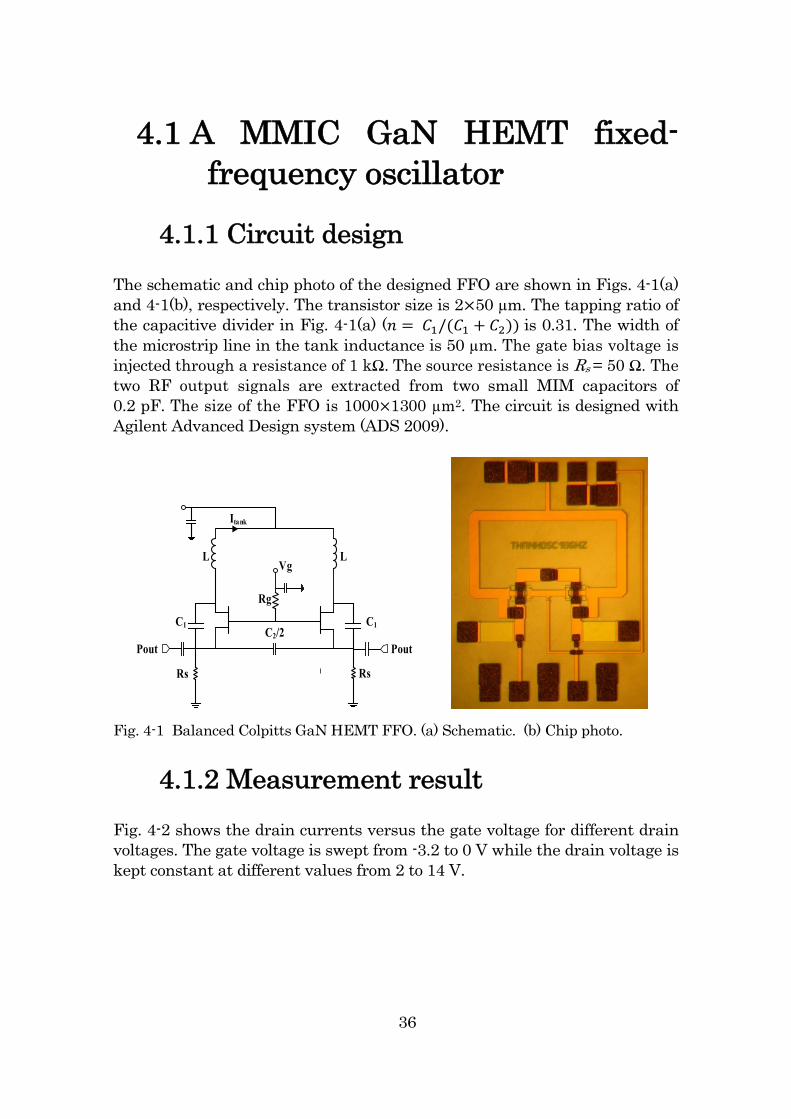
The schematic and chip photo of the designed FFO are shown in Figs. 4-1(a) and 4-1(b), respectively. The transistor size is 2 50 µm. The tapping ratio of the capacitive divider in Fig. 4-1(a) ( / is 0.31. The width of the microstrip line in the tank inductance is 50 µm. The gate bias voltage is injected through a resistance of 1 kΩ. The source resistance is Rs = 50 Ω. The two RF output signals are extracted from two small MIM capacitors of 0.2 pF. The size of the FFO is 1000 1300 µm2. The circuit is designed with Agilent Advanced Design system (ADS 2009).
VgL L
Rg
C1 C1C2/2
Pout
Rs Rs
Itank
Pout
Fig. 4-1 Balanced Colpitts GaN HEMT FFO. (a) Schematic. (b) Chip photo.
4.1.2 Measurement result
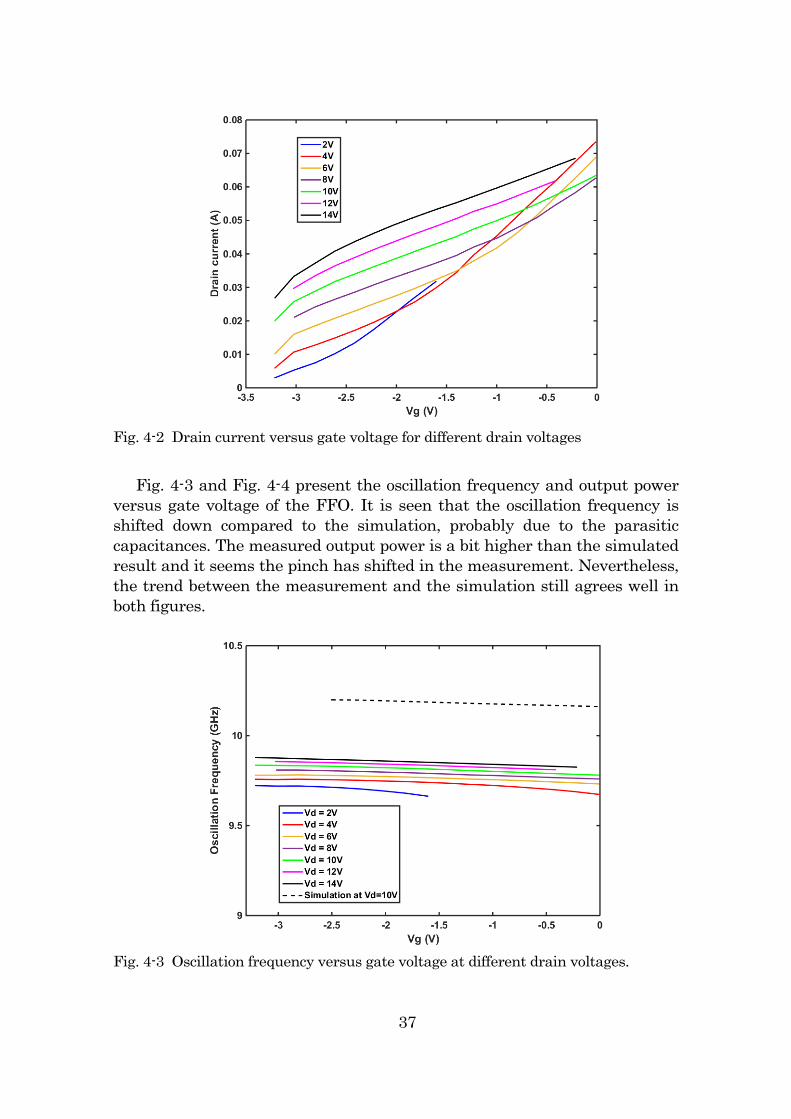
Fig. 4-2 shows the drain currents versus the gate voltage for different drain voltages. The gate voltage is swept from -3.2 to 0 V while the drain voltage is kept constant at different values from 2 to 14 V.
37
Fig. 4-2 Drain current versus gate voltage for different drain voltages
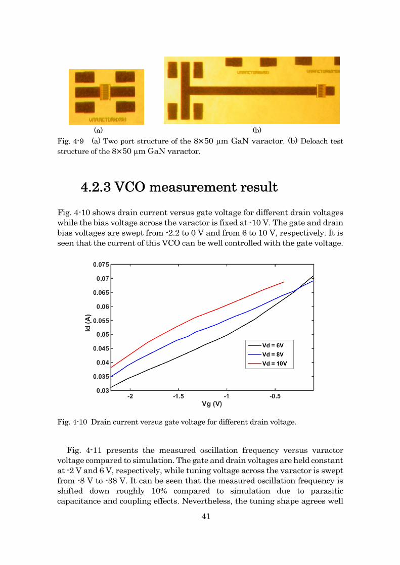
Fig. 4-3 and Fig. 4-4 present the oscillation frequency and output power
versus gate voltage of the FFO. It is seen that the oscillation frequency is shifted down compared to the simulation, probably due to the parasitic capacitances. The measured output power is a bit higher than the simulated result and it seems the pinch has shifted in the measurement. Nevertheless, the trend between the measurement and the simulation still agrees well in both figures.
Fig. 4-3 Oscillation frequency versus gate voltage at different drain voltages.

38
Fig. 4-4 Output power versus gate voltage at different drain voltages.
Measured phase noise versus offset frequency for the FFO is shown in
Fig. 4-5. Fig. 4-6 presents a contour plot of the phase noise at 100 kHz offset for all bias points. It is found that the best phase noise of this FFO is about -100 dBc/Hz @ 100 kHz for a bias point Vd /Vg = 6 V/-3.2 V.
Fig. 4-5 Measured phase noise versus offset frequency of the FFO with bias condition as parameter.

39
Fig. 4-6 100 kHz phase noise versus drain and gate bias voltage.
4.2 A MMIC GaN HEMT Voltage-Controlled Oscillator
4.2.1 Circuit design
Fig. 4-7 Balanced Colpitts GaN HEMT VCO. (a) Schematic. (b) Chip photo.

40
In Figs. 4-7(a) and 4-7(b), respectively, the schematic and chip photo of the designed VCO are shown.
Similar to the GaN HEMT FFO described in section 4.1, the transistor size used in this VCO is 2 50 µm. The component values in the schematic are chosen for optimum phase noise. The tapping ratio ( / is 0.3. A varactor size of 8 50 µm is chosen for wide tuning range. Due to the limitation of varactor dimensions, two varactors are combined in parallel in order to reach the desired capacitance value. The gate resistance is Rg =1 kΩ and the source resistance is Rs = 50 Ω. The output signal is extracted from a small MIM capacitance of 0.2 pF at one RF port while the other RF port is open. The size of the VCO is 1300 1400 µm2. The VCO is designed with ADS 2009.
4.2.2 Varactor characterization
Fig. 4-8 presents the extracted C(V) and Q(V) at 10 GHz of the 8 50 µm GaN varactor used versus the tuning voltage. Varactor capacitance C(V) is extracted from a two-port structure with two-port S-parameter characterization, see Fig. 4-9 (a), while Q-factor is extracted from a Deloach test structure, see Fig. 4-9 (b), based on the method described in section 2.5. It can be seen that the Q-factor is poor for bias voltage > -5 V. Thus, the useful tuning range is defined to be between -5 V to -40 V. Below -25 V, the capacitance variation of the varactor decreases significantly.
Fig. 4-8 Extracted varactor capacitance and Q-factor at 10 GHz versus the tuning voltage of the 8 50 µm varactor.
41
(a) (b)
Fig. 4-9 (a) Two port structure of the 8 50 µm GaN varactor. (b) Deloach test structure of the 8 50 µm GaN varactor.
4.2.3 VCO measurement result
Fig. 4-10 shows drain current versus gate voltage for different drain voltages while the bias voltage across the varactor is fixed at -10 V. The gate and drain bias voltages are swept from -2.2 to 0 V and from 6 to 10 V, respectively. It is seen that the current of this VCO can be well controlled with the gate voltage.
Fig. 4-10 Drain current versus gate voltage for different drain voltage.
Fig. 4-11 presents the measured oscillation frequency versus varactor
voltage compared to simulation. The gate and drain voltages are held constant at -2 V and 6 V, respectively, while tuning voltage across the varactor is swept from -8 V to -38 V. It can be seen that the measured oscillation frequency is shifted down roughly 10% compared to simulation due to parasitic capacitance and coupling effects. Nevertheless, the tuning shape agrees well

42
between measurement and simulation. The VCO has a tuning bandwidth of 1.1 GHz (6.45-7.55 GHz), corresponding to a tuning range about 15%.
Fig. 4-11 Oscillation frequency and phase noise versus tuning voltage of the varactor.
Fig. 4-12 presents the measured and simulated output power versus tuning
voltage of the varactor. The measured power is 1.5 dB higher than the simulated. Similar to the oscillation frequency, the shape of measured and simulated output power agree well. The output power varies from –2 dBm to 2 dBm.
Fig. 4-12 Oscillator output power versus tuning voltage of the varactor.
43
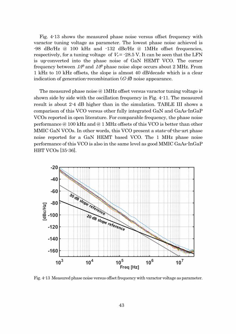
Fig. 4-13 shows the measured phase noise versus offset frequency with varactor tuning voltage as parameter. The lowest phase noise achieved is -98 dBc/Hz @ 100 kHz and -132 dBc/Hz @ 1MHz offset frequencies, respectively, for a tuning voltage of Vv = -28.5 V. It can be seen that the LFN is up-converted into the phase noise of GaN HEMT VCO. The corner frequency between 1/f3 and 1/f2 phase noise slope occurs about 2 MHz. From 1 kHz to 10 kHz offsets, the slope is almost 40 dB/decade which is a clear indication of generation-recombination (G-R) noise appearance.
The measured phase noise @ 1MHz offset versus varactor tuning voltage is
shown side by side with the oscillation frequency in Fig. 4-11. The measured result is about 2-4 dB higher than in the simulation. TABLE III shows a comparison of this VCO versus other fully integrated GaN and GaAs-InGaP VCOs reported in open literature. For comparable frequency, the phase noise performance @ 100 kHz and @ 1 MHz offsets of this VCO is better than other MMIC GaN VCOs. In other words, this VCO present a state-of-the-art phase noise reported for a GaN HEMT based VCO. The 1 MHz phase noise performance of this VCO is also in the same level as good MMIC GaAs-InGaP HBT VCOs [35-36].
Fig. 4-13 Measured phase noise versus offset frequency with varactor voltage as parameter.

44
4.3 Accurate phase noise simulation
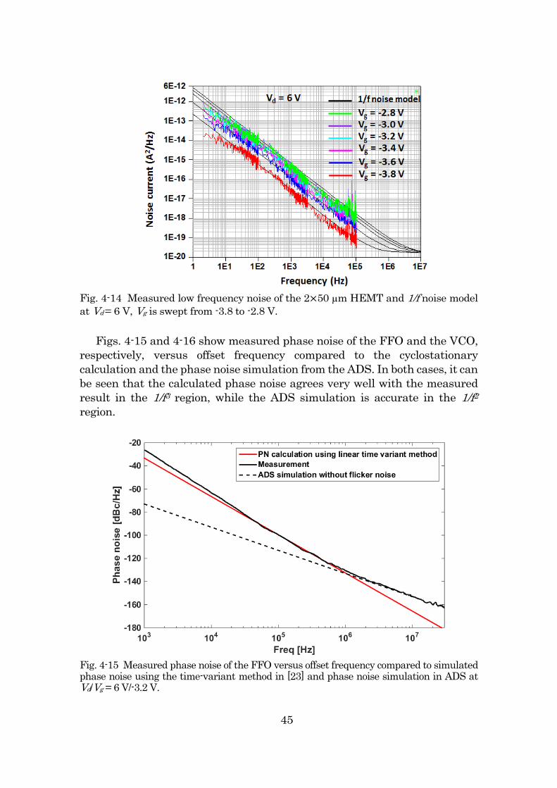
Agilent ADS is used for the simulations of the GaN HEMT FFO and VCO. However, the phase noise simulation in ADS does not include the flicker noise model. Therefore, this work addresses the method proposed in [23] to accurately predict the phase noise of a GaN HEMT oscillator. To apply this method, a LFN measurement and oscillator waveforms from a HB simulation, i.e. transistor intrinsic current, tank resonance current, tank resonance voltage, are required. Fig. 4-14 shows the measured low frequency noise of the 2 50 µm HEMT compared to the 1/f noise model mentioned in section 2.3.3 for Vd = 6 V and Vg being swept from -3.8 to -2.8 V. The setup used is setup B, referring to chapter 3. The extracted values of the constants in the flicker noise model are: Kf = 1.3e-10, Af = 0.8, fFE = 1.3.
TABLE ICOMPARISON TO OTHER MMIC GAN AND INGAP HBT VCOS
Technology Frequency(GHz)
Pout
(dBm)PN @ 100
kHz PN @1 MHz
Ref
(dBc/Hz) (dBc/Hz) fmin fmax BW
GaN HEMT 9.11 9.55 0.4 3.3 -82 -110 [10] GaN HEMT 8.5 9.5 1.0 31.8 -77 -101 [11] GaN HEMT 6.5 7.5 1.0 17 -81 -110 [12] GaN HEMT 6.45 7.55 1.1 2 -98 -132 This
work InGaP HBT 6.1 7.5 1.4 -5 -102 -125 [14] InGaP HBT 8.0 9.7 1.7 7 -106 -128 [15]
45
Fig. 4-14 Measured low frequency noise of the 2 50 µm HEMT and 1/f noise model at Vd = 6 V, Vg is swept from -3.8 to -2.8 V.
Figs. 4-15 and 4-16 show measured phase noise of the FFO and the VCO,
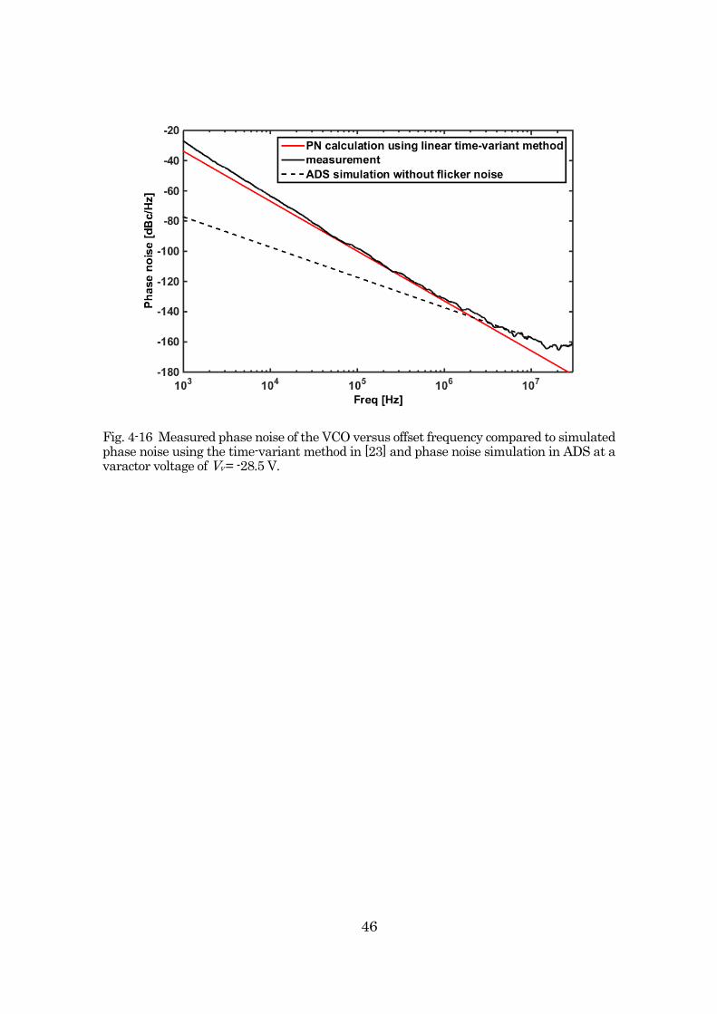
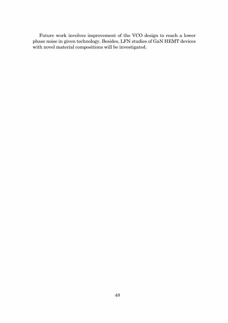
respectively, versus offset frequency compared to the cyclostationary calculation and the phase noise simulation from the ADS. In both cases, it can be seen that the calculated phase noise agrees very well with the measured result in the 1/f3 region, while the ADS simulation is accurate in the 1/f2 region.
Fig. 4-15 Measured phase noise of the FFO versus offset frequency compared to simulated phase noise using the time-variant method in [23] and phase noise simulation in ADS at Vd/Vg = 6 V/-3.2 V.
46
Fig. 4-16 Measured phase noise of the VCO versus offset frequency compared to simulated phase noise using the time-variant method in [23] and phase noise simulation in ADS at a varactor voltage of Vv = -28.5 V.

47
Conclusions This thesis presents LFN characterization and comparison of several different III-V transistor technologies, e.g., GaAs-InGaP HBT, GaAs pHEMT, and GaN HEMT. The characterization targets low phase noise oscillator design and with the motivation that phase noise is inversely proportional power, LFN normalized to DC power is used as a benchmark parameter. It is verified that the best performance in term of both absolute noise level and normalized value is obtained for GaAs-InGaP HBT, in particular for low frequency. For higher frequencies, GaN HEMTs have potential for better performance due to less shot noise compared to GaAs-InGaP HBT technology. Thus, GaN HEMT is an attractive transistor technology for oscillator applications where phase noise at far off-set frequencies is of concern.
Then, an in-depth investigation on some factors which influence LFN characteristic of III-N GaN based HEMTs, i.e. AlGaN/GaN based HEMTs and AlInN/AlN/GaN based HEMTs with different surface passivation methods (Al2O3 thermal ALD, Al2O3 plasma-assisted ALD and Si3N4 PECVD) and variations in transistor geometry (gate length, gate width and source to drain distance) are studied. It is found that the surface passivation has considerable impact on the LFN while transistor geometry has only marginal effect. The lowest noise is achieved for samples passivated with Al2O3 deposited with thermal ALD.
Furthermore, two MMIC circuits: a GaN HEMT based FFO and a GaN HEMT based VCO have been designed. Fairly good phase noise is demonstrated for both circuits. The GaN HEMT FFO, with an oscillation frequency of 10 GHz presents a phase noise of -100 dBc/Hz @ 100 kHz offset from the carrier. The GaN HEMT VCO has a tuning range of 15% (6.45-7.55 GHz) with nearly constant output power, high tuning linearity and good phase noise. Its phase noise performance at 1 MHz off-set is better than state-of-the-art InGaP HBT VCOs with comparable oscillation frequency and tuning range. Beside good performance, the measured phase noise in the 1/f3 region of both circuits is well predicted with a time variant phase noise model.
48
Future work involves improvement of the VCO design to reach a lower phase noise in given technology. Besides, LFN studies of GaN HEMT devices with novel material compositions will be investigated.
49
Acknowledgements
First of all, I would like to express my gratitude to my examiner Prof. Herbert Zirath for giving me an opportunity to work in the Microwave Electronics Laboratory and for helping me with the redaction of my thesis. I am also grateful to Prof. Jan Grahn, Director of the GHz Center, for giving me a chance to work in the GHz Center.
I would like to express my deepest gratitude to my supervisor, Assoc. Prof. Dan Kuylenstierna for his daily guidance, advice and support in my research. Thanks for his help given whenever I need, his careful review of this thesis and manuscripts, his valuable discussions which broaden my knowledge, his continuous encouragement throughout my up and down time.
I also would like to thank my assistant supervisor Dr. Szhau Lai for his help in the lab and in the circuit design. Thanks to Mikael Hörberg, Dr. Mingquan Bao and Thomas Emanuelsson for their help in the project and for many creative ideas and fruitful discussions that they have shared with me.
I would like to acknowledge Assoc. Prof. Niklas Rorsman for guiding me through many new things in the device field and for helping me with manuscript proofreading. I am also grateful to Anna Malmros and Johan Bergsten for providing me with your devices.
I would like to thank Assoc. Prof. Vessen Vassilev for guiding me through many measurement techniques before I started my PhD. Thanks my friend, Yu Yan, for daily funny chats and thanks all colleagues at the Microwave Electronics Laboratory for creating a nice research environment.
Finally, I would like to express my special thanks to my family: my parents, my sisters, my beloved husband and my little sweet angel Annie for their unconditional love, care and support.
* This research has been carried out in GigaHertz Centre in a joint project
financed by the Swedish Governmental Agency for Innovation Systems (VINNOVA), Chalmers University of Technology, Ericsson AB, and RUAG Space AB.

50

51
References S. Wu, Y.Bar-Ness, “OFDM in the presence of phase noise: consequences
and solutions,” IEEE Trans. on Communications, vol. 52, no. 11, pp. 1988-1996, 2004.
A. Hajimiri, T. Lee, “The Design of Low Noise Oscillators”, Boston: Kluwer Acedemic Publishers, 1999.
C. Sanabria, “Noise of AlGaN/GaN HEMTs and Oscillators”, PhD dissertation, Department of Electrical and Computer Engineering, University of California Santa Barbara, pp. 101-125, June 2006.
D. B. Leeson, “A simple model of feedback oscillator noise spectrum”, in Proceedings of the IEEE 54(2), pp. 329-330, 1996.
S. Rumyantsev, M. E. Levinshtein, R. Gaska, M. S. Shur, A. Khan, J. W. Yang, G. Simin, A. Ping, T. Adesida, “Low 1/f Noise in AlGaN/GaN HFETs on SiC Subtrates”, in Proc. 3rd International Conference on Nitride Semiconductors (ICNS3), vol.176, Montpellier, France, July 1999, phys. stat. sol. (a), pp. 201-204.
S. Mohammadi, D. Pavlidis, B. Bayraktaroglu, “Relation Between Low-Frequency Noise and Long-Term Reliability of Single AlGaAs/GaAs Power HBT’s”, IEEE Trans. Electron Devices, Vol. 47, No.4, pp. 677-686, April 2000.
W. Lu, V. Kumar, R. Schwindt, E. Piner, I. Adesida, “A comparative study of surface passivation on AlGaN/GaN HEMTs,” Solid-State Electronics, vol. 46, pp. 1441-1444, Jan. 2002.
H. Wang, J. W. Chung, X. Gao, S. Guo, T. Palacios, “Al2O3 passivated InAlN/AlN/GaN HEMT on SiC substrate with record current density and transconductance,” Phys. Status Solidi C, vol. 7, no. 10, pp. 2440-2444, Jun. 2010.
A. V. Vertiatchikh, L.F. Eastman, “Effect of the Surface and Barrier Defects on the AlGaN/GaN HEMT Low-Frequency Noise Performance,” IEEE. Electron Device Lett., vol. 24, no. 9, pp. 535-537, Sept. 2003.
Z. Q. Cheng, Y. Cai, J. Liu, Y. Zhou, K. M. Lau, K.J. Chen, “A Low Phase Noise X- Band MMIC VCO Using High-Linearity and Low-Noise Composite-Channel Al0.3Ga0.7N/Al0.05Ga0.95N/GaN HEMTs,” IEEE Trans. Microwave Theory & Tech., vol. 55, no. 1, pp. 23-29, 2007.

52
V. Kaper, R. Thompson, T. Prunty, J. R. Shealy, “X-band AlGaN/GaN HEMT MMIC Voltage- Controlled Oscillator,” in Proceedings of 11th Gallium Arsenide applications (GAAS) Symposium, pp. 45-48, 2003.
C. Kong, H. Li, X. Chen, S. Jiang, J. Zhou, C. Chen, “A Monolithic AlGaN/GaN HEMT VCO Using BST Thin-Film Varactor,” IEEE Trans. Microwave Theory & Tech., vol. 60, no. 11, pp. 3413-3419, 2012.
H. Zirath, R. Kozhuharov, M. Ferndahl, “Balanced Colpitts-oscillator MMICs designed for ultra-low phase noise,” IEEE J. Solid-State Circuits, vol. 40, no. 10, pp. 2077-2086, 2005.
H. Zirath, “Low phase-noise balanced Colpitt InGaP-GaAs HBT VCOs with wide frequency tuning range and small VCO- gain variation,” in IEEE Asia-Pacific Micro. Conf, Thailand, Dec. 11-14, 2007.
D. Kuylenstierna, S. Lai, B. Mingquan, H. Zirath, “Design of Low-Phase-Noise Oscillators and Wideband VCOs in InGaP-HBT Technology,” IEEE Trans. Microwave Theory &Tech., vol. 60, pp. 3420-3430, 2012.
D. Baek, K. Sangsoo, K. Jeong-Geun, K. Dong-Wook, H. Songcheol, “Ku-band InGaP-GaAs HBT MMIC VCOs with balanced and differential topologies,” IEEE Trans. Microwave Theory &Tech., vol. 52, pp. 1353-1359, 2004.
B. Mingquan, L. Yinggang, H. Jaconsson, “A 25 GHz ultra-low phase noise InGaP/GaAs HBT VCO,” IEEE Microw. Compon. Lett., vol.15, pp. 751-753, 2005.
Y. G. Kim, J. H. Bae, C. Park, C. W. Kim, S. Kim, B. G. Min, J-M. Lee, H. J. Kim, K. H. Lee, “An X- band INGaP GaAs HBT MMIC oscillator,” Current Applied Physics, vol. 5, pp. 249-253, 2005.
M. Hörberg, T. Emanuelsson, S. Lai, T. N. T. Do, H. Zirath, D. Kuylenstierna, “Phase Noise Analysis of an X-band Ultra-low Phase Noise GaN HEMT based Cavity Oscillator,” IEEE Trans. Microwave Theory &Tech., vol. 63, pp. 2619-2629, 2015.
S. Lai, D. Kuylenstierna, M. Özen, M. Hörberg, N. Rorsman, I. Angelov, et al.,“Low Phase Noise GaN HEMT Oscillators With Excellent Figures of Merit,” IEEE Microw. Compon. Lett., vol.24, pp. 412-414, 2014.
M. Hörberg, D. Kuylenstierna, “Low phase noise power-efficient MMIC GaN HEMT Oscillator at 15 GHz based on a Quasi-lumped on chip resonator,” in IEEE MTT-S International Microwave Symposium Digest, 17-22 May, Phoenix, Arizona, 2015, pp. 1-4.
G. Soubercaze-Pun, J. G. Tartarin, L. Bary, J. Rayssac, E. Morvan, B. Grimbert, et. al., “Design of a X-band GaN oscillator: From the low frequency noise device characterization and large signal modeling to circuit design,” in IEEE MTT-S International Microwave Symposium Digest, 11-16 June, 2006, pp. 745-750.
53
S. Lai, D. Kuylenstierna, M. Hörberg, N. Rorsman, I. Angelov, K. Andersson, H. Zirath, “Accurate Phase noise Prediction for a balanced Colpitts GaN HEMT MMIC Oscillator,” IEEE Trans. Microwave Theory & Tech., vol. 61, no. 11, pp. 3916-3926, Nov., 2013.
R. S. Pengelly, et al., "A review of GaN on SiC high electron-mobility power transistors and MMICs," IEEE Transactions on Microwave Theory and Techniques, vol. 60, pp. 1764-83, 2012.
M. Özen and C. Fager, "Symmetrical doherty amplifier with high efficiency over large output power dynamic range," in IEEE MTT-S International Microwave Symposium, 2014, pp. 1-4.
S. Voinigescu, “High-Frequency Integrated Circuits”, Cambridge University Press, 2013.
P. R. Gray, P. J. Hurst, S. H. Lewis, R. G. Meyer, “Analysis and Design of Annalog Integrated Circuits”, John Wiley & Sons, Itc., 2010.
F. N. Hooge, “1/f Noise Sources”, IEEE Trans. Electron Devices, vol. 41, no. 11, pp. 1926-1935, Nov.1994.
A. Balandin, S. Morozov, S. Cai, R. Li, K. Wang, G. Wijeratne, C. Viswanathan, “Low Flicker-Noise GaN/AlGaN Heterostructure Field-Effect Transistors for Microwave Communications, ” IEEE Trans. Microwave Theory & Tech., vol. 47, no. 8, pp. 1413–1417, 1999.
S. H. Hsu, J. S. Moon, M. Micovic, D. Wong, T. Hussain, “Characterization and analysis of gate and drain low-frequency noise in AlGaN/GaN HEMTs,” Proc. IEEE. Lester Eastman Conf. on High Performance Devices, pp. 453-460, 2002.
J. Peransin, P.Vignaud, D. Rigaud, L. Vandamme, “1/f noise in MODFET’s at low drain bias”, IEEE Trans. Electron Devices, vol. 37, pp. 2250-2253, Oct. 1990.
L. K. J. Vandamme, H. M. M. de Werd, “1/f noise model for MOSTs biased in nonohmic region”, IEEE Solid-State Electronics, vol. 23, pp. 325-329, 1980.
A. V. Vertiatchikh, L.F. Eastman, “Effect of the Surface and Barrier Defects on the AlGaN/GaN HEMT Low-Frequency Noise Performance,” IEEE. Electron Device Lett., vol. 24, no. 9, pp. 535-537, Sept. 2003.
V. Mitin, L. Reggiani, L. Varani, “Noise and Fluctuations Control in Electronic Devices,” American Scientific Publishers, 2002.
T. H. Lee, A. Hajimiri, “Oscillator Phase Noise: A Tutorial,” IEEE. Solid- State Circuits, vol. 35, no. 3, pp. 326-336, Mar. 2000.
J. Everard, Min Xu, S. Bale, “Simplified phase noise model for negative-resistance oscillators and a comparison with feedback oscillator models,” IEEE Transactions on Ultrasonics, Ferroelectrics and Frequency Control, vol. 59, no. 3, pp. 382-390, March 2012.
54
A. Hajimiri, T. H. Lee, “A General Theory of Phase Noise in Electrical Oscillators,” IEEE. Solid- State Circuits, vol. 33, no. 2, pp. 179-194, Feb. 1998.
B. C. Deloach, “A new microwave measurement technique to characterize diodes and an 800-gc cutoff frequency varactor at zero volts bias,” IEEE Trans. Microwave Theory & Tech., vol. 12, no. 1, pp. 15-20, 1964.
F. Sischka, “1/f noise measurements and modeling”, Agilent Technologies Company, 2002.
P. Sakalas, A. Simukovic, S. Piotrowicz, O. Jardel, S. L. Delage, A. Mukherjee, A. Matulionis, “Compact modelling of InAlN/GaN HEMT for low noise applications,” Semicond. Sci. Technol., vol. 29, Aug. 2014.
C. Kayis, C. Y. Zhu, M. Wu, X. Li, U. Ozgur, H. Morkoc, “Low-frequency noise measurements of electrical stress in InAlN/GaN and AlGaN/GaN heterostructure filed-effect transistors,” Proc. of SPIE, vol. 7939, p. 79392G, Mar.2011.
M.-A. di Forte-Poisson, N. Sarazin, M. Magis, M. Tordjman, J. Di Persio, R. Langer, E. Iliopoulos, A. Georgakilas, P. Kominou, M. Guziewicz, E. Kaminska, A. Piotrowska, C. Gaquière, M. Oualli, E. Chartier, E. Morvan, and S. Delage, “LP MOCVD growth of InAlN/GaN HEMT heterostructure: comparison of sapphire, bulk SiC and composite SiCopSiC substrates for HEMT device applications”, Phys. Stat. Sol. (C), vol. 7, no. 5, pp. 1317-24, Mar. 2010.
A. Malmros, P. Gamarra, M-A di Forte-Poisson, H. Hjelmgren, C. Lacam, M. Thorsell, M. Tordjman, R. Aubry, N. Rorsman, “Evaluation of Thermal Versus Plasma-Assisted ALD Al2O3 as Passivation for InAlN/AlN/GaN HEMTs,” IEEE. Electron Device Lett., vol. 36, no. 3, pp. 235-237, Feb. 2015.