geiger-mode ladar cameras - spectrolab · geiger-mode ladar cameras ping yuan *, rengarajan...
TRANSCRIPT
Geiger-mode LADAR cameras
Ping Yuan*, Rengarajan Sudharsanan, Xiaogang Bai, Joseph Boisvert, Paul McDonald, and Eduardo Labios
Spectrolab Inc., a Boeing Company, 12500 Gladstone Ave., Sylmar, CA, USA 91342
Bryan Morris, John P Nicholson, Gary M Stuart, and Harrison Danny Boeing DES, 4411 The 25 Way NE # 350, Albuquerque, NM 87109
Stephen Van Duyne, Greg Pauls, and Stephen Gaalema
Black Forest Engineering, LLC, 1879 Austin Bluffs Parkway, Colorado Springs, CO 80918
ABSTRACT The performance of Geiger-mode LAser Detection and Ranging (LADAR) cameras is primarily defined by individual pixel attributes, such as dark count rate (DCR), photon detection efficiency (PDE), jitter, and crosstalk. However, for the expanding LADAR imaging applications, other factors, such as image uniformity, component tolerance, manufacturability, reliability, and operational features, have to be considered. Recently we have developed new 32x32 and 32x128 Read-Out Integrated Circuits (ROIC) for LADAR applications. With multiple filter and absorber structures, the 50-μm-pitch arrays demonstrate pixel crosstalk less than 100 ppm level, while maintaining a PDE greater than 40% at 4 V overbias. Besides the improved epitaxial and process uniformity of the APD arrays, the new ROICs implement a Non-uniform Bias (NUB) circuit providing 4-bit bias voltage tunability over a 2.5 V range to individually bias each pixel. All these features greatly increase the performance uniformity of the LADAR camera. Cameras based on these ROICs were integrated with a data acquisition system developed by Boeing DES. The 32x32 version has a range gate of up to 7 μs and can cover a range window of about 1 km with 14-bit and 0.5 ns timing resolution. The 32x128 camera can be operated at a frame rate of up to 20 kHz with 0.3 ns and 14-bit time resolution through a full CameraLink. The performance of the 32x32 LADAR camera has been demonstrated in a series of field tests on various vehicles.
1. INTRODUCTION AND BACKGROUND The recent progress in the short wavelength infrared region (SWIR) three-dimension imaging provides an important solution for foliage penetration, camouflage imaging, and aerial mapping in battlefield intelligence and Earth survey. Its airborne applications, which make the most potential market for this technology, have posted a series of challenges to the camera. Because the laser and its service system take most of the size, weight, and power (SWAP) of a LADAR system, it is critical to maximize the camera sensitivity to reduce the laser power requirement in order to enhance the ranging distance and reduce the SWAP of the whole system. InP-based single-photon counting GM-APDs fit perfectly to this requirement. Geiger-mode avalanche photodiode focal plane arrays (GM-FPAs) have been reported by both MIT Lincoln Laboratory1 and Boeing Spectrolab2 for SWIR applications. Due to the availability of high power emitters, most of the effort to date has been focused on photodiodes operating at 1.06 µm. Important figures of merits for GM-APDs include dark count rate (DCR) and photon detection efficiency (PDE) which together establish the upper limit of the signal-to-noise ratio for the entire sensor system. For active 3-D imaging, sensor’s FPA timing jitter and crosstalk are also critical because the jitter sets the upper limit of range resolution while the latter greatly influences the spatial resolution. Frame rate limits the sensor update time which is also a critical performance parameter in airborne applications. Since it is primarily determined by the data process and download rate, the GM-APD afterpulsing, or temporal crosstalk between range gates, is normally not a great concern in imaging applications as long as it is no less than 100 kHz. Other important parameters include weight, power, and volume. Because most of the power consumed in a LADAR camera is by the thermoelectric coolers (TEC), a higher APD operation temperature is always welcome to airborne applications. * Email: [email protected]; Tel: 818 898 7578; Fax : 818 838 7474.
Laser Radar Technology and Applications XVI, edited by Monte D. Turner, Gary W. Kamerman,Proc. of SPIE Vol. 8037, 803712 · © 2011 SPIE · CCC code: 0277-786X/11/$18 · doi: 10.1117/12.884346
Proc. of SPIE Vol. 8037 803712-1
Downloaded from SPIE Digital Library on 27 Oct 2011 to 130.76.64.116. Terms of Use: http://spiedl.org/terms
Spectrolab and Black Forest Engineering have been working under DARPA Elusive Surface Target Engagement Technology program to advance the performance of both the avalanche photodiode detector and ROIC arrays that together comprise an FPA. Black Forest Engineering has designed a new 32x32 ROIC with enhanced capabilities that include: a non-uniform bias (NUB) correction that can be applied to individual pixels across the array; and a modified pixel input circuit that effectively removes high dark current (shorted) APD pixels from the array to reduce the overall current draw that would otherwise cause an FPA to fail. Spectrolab has introduced a feature to the APD detector array that reduces the optical crosstalk between pixels to <100ppm and reduces Dark Count Rate (DCR) at operating temperature to <10 kHz. External PDE on detectors alone, without a microlens, in excess of 40% has been demonstrated for reverse-illuminated arrays.
Parameter Spec Test conditions Wavelength 1.06 µm
Format 32x32
Pixel Pitch 100 µm
PDE 40% 240K, 4V overbias
Fill Factor 70%
DCR 20 kHz 240K, 4V overbias
Cross talk <1% Optimized overbias for SCA
Pixel operability 99%
RMS timing jitter 0.5 ns
Table 1. Typical single photon counting focal plane array figures of merits for a 32x32 GM-APD array presently fabricated at Spectrolab.
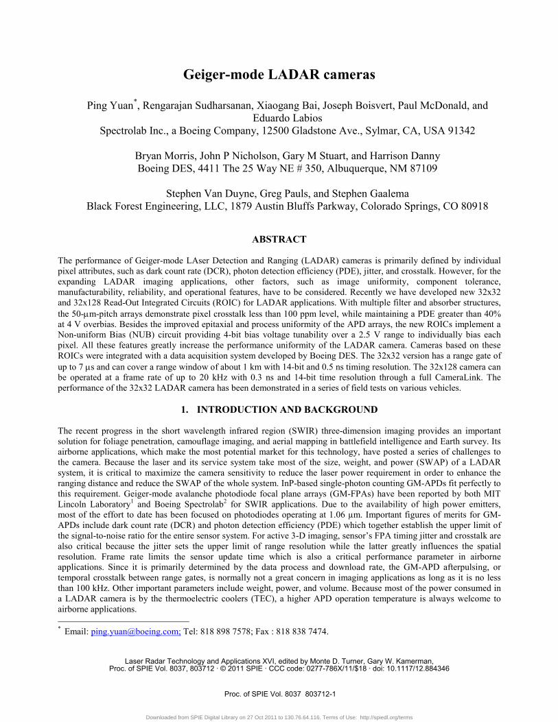
Figure 1. Geiger-mode operation of an avalanche photodiode. The left panel shows the typical IV
characteristics of a 200 um GM-APD under illumination and in dark. The linear mode region
1.E-10
1.E-09
1.E-08
1.E-07
1.E-06
1.E-05
1.E-04
35 40 45 50 55 60 65 70 75 80 85Voltage (V)
Cur
rent
(A)
timetime
timetime
time
Single photon input
APD output
Digital comparator output
Successfulsingle photondetection
Photon absorbed but insufficient gain – missed count
Dark count –from dark current
Geiger-mode operation
timetime
timetime
time
Single photon input
APD output
Digital comparator output
Successfulsingle photondetection
Photon absorbed but insufficient gain – missed count
Dark count –from dark current
Geiger-mode operation
is highlighted in blue, while the Geiger-mode operation region is shaded in red. The right panel illustrated the three possible cases in Geiger-mode detection.
Proc. of SPIE Vol. 8037 803712-2
Downloaded from SPIE Digital Library on 27 Oct 2011 to 130.76.64.116. Terms of Use: http://spiedl.org/terms
All these parameters mentioned above must be optimized for the optimal sensor performance. In practice these parameters are not decoupled and often trade off against one another. A robust FPA read out integrated circuit (ROIC) can improve sensor performance by mitigating APD deficiencies. However, an FPA design is fundamentally limited by detector performance. Table 1 lists the most important FPA figures of merit that impact single photon counting sensor systems.
2. GM-APD FPA FUNDAMENTALS In Geiger-mode operation the avalanche photodiodes are biased above the breakdown voltage, ~ 2-4 V, for a short period of time during which the sensor is active. If a photon in the sensitive spectrum falls on the detector pixel in this period, it has a probability to be absorbed and multiplied in the GM-APD such that the amplitude of the result pulse is large enough to be converted into a digital pulse that can be registered by the following readout circuit. This probability is a figure of merit called photon detection efficiency (PDE). Due to various carrier generation mechanisms in GM-APDs, there is still some probability for the pixels to generate some output pulses even without any incident photons. This probability is characterized by dark count rate (DCR) and it represents the noise of GM-APD arrays. Typically DCR increases with overbias and operating temperature. Because a higher overbias also yields a better PDE, for a better signal-to-noise ratio, the trade-off between PDE and DCR has to be carefully considered in the device operation point selection. Figure 1 details the general concepts of Geiger-mode operation.
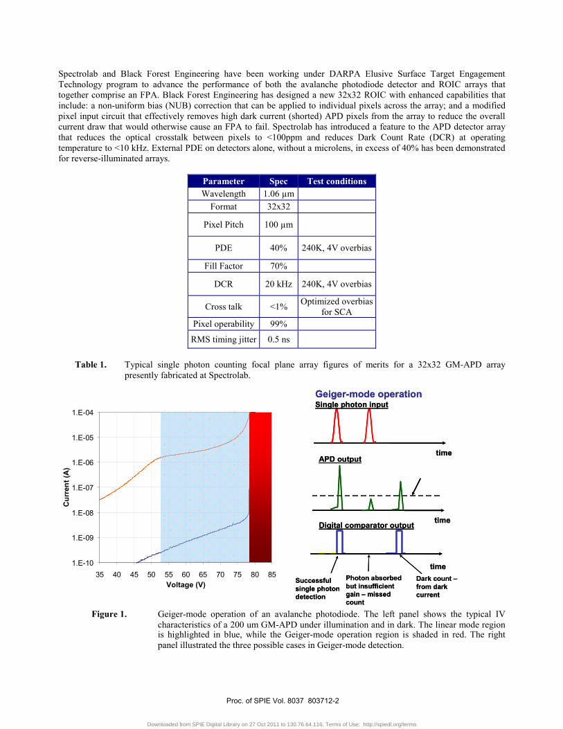
Figure 2. 1.06 µm GM-APD device design and resultant electric field profile during operation.
Figure 2 shows the InGaAsP/InP GM-APD separate absorption and gain and multiplication (SAGM) device structure for 1.06 µm operation. The multiplication layer and silicon doped charge layer are both formed with InP. An InGaAsP alloy is used in the absorption layer for 1.06-µm photons. The right panel shows the electric field profile at operation in this device structure. With a carefully controlled charge layer, the electric filed in the multiplier is high for appreciable avalanche gain and it is low across the absorption layer to prevent tunneling of carrier so that the DCR is low in these
P-P-
i-
PP-
i
InP Buffer 2InP Buffer 1
InP Multiplier
-
-
P-P-
i-
PP-
i
InP Buffer 2InP Buffer 1
InP Multiplier
-
-
InP Buffer 2InP Buffer 1
InP Multiplier
-InP Buffer 2InP Buffer 1
InP Multiplier
InP Buffer 2InP Buffer 1
InP Multiplier
-
-
N-InP Charge layer
InGaAsP Graded layer
i-InGaAs
n-InPn-InGaAs
N-InP Charge layer
InGaAsP Graded layer
InGaAs or InGaAsP
n-InPn-InGaAs
InP Substrate
N-InP Charge layer
InGaAsP Graded layer
i-InGaAs
n-InPn-InGaAs
N-InP Charge layer
InGaAsP Graded layer
InGaAs or InGaAsP
n-InPn-InGaAs
N-InP Charge layer
InGaAsP Graded layer
i-InGaAs
n-InPn-InGaAs
N-InP Charge layer
InGaAsP Graded layer
InGaAs or InGaAsP
n-InPn-InGaAs
InP Substrate
E
InGaAs(P)Absorber
he
InGaAs(P)Absorber
he
P Substrate
InP MultiplierGain = ∞
hν P Substrate
InP MultiplierGain = ∞
hν
InP MultiplierGain = ∞
hνhν
Proc. of SPIE Vol. 8037 803712-3
Downloaded from SPIE Digital Library on 27 Oct 2011 to 130.76.64.116. Terms of Use: http://spiedl.org/terms

devices. The top N+ InGaAs layer is used as a contact layer. The nominal thickness the InGaAsP absorption layer is 1.5 µm for good quantum efficiency. The device growth and characterization details have been described in previous literatures2.
3. SINGLE DEVICE PERFORMANCE
As described earlier2, single element mesa devices with different mesa diameters, from 20 µm to 200 µm, are fabricated to evaluate the quality of epitaxial wafers. Initial I-V testing is done at room temperature to determine the breakdown voltage, punch through voltage, and leakage current. The device optical gain and responsivity were measured by illuminating with a 1.06 µm wavelength laser. The left panel of Figure 1 shows the dark current and gain versus bias characteristics of a 200 µm diameter device. The bulk current density referred to unity gain is a typical figure of merit for APDs and in this case JD(M=1)=630 nA/cm2. The most important figure of merits of GM APDs are DCR and PDE, and together they define the signal-to-noise ratio of the whole photon counting system. Because both increase with the overbias, it is critical to trade off between them in operation. The device optimization principles and strategies have been reported previously by Lincoln Laboratory3 and Spectrolab4 Figure 3 plots the PDE against DCR of three 25-μm array pixels on a 32x128 GM APD array under different overbiases and 243K. Grown on p-type InP substrates, the devices can achieve 40% PDE with 3~4 kHz DCR at the operation temperature.
Figure 3. PDE as function of DCR of three typical Spectrolab 25-µm diameter Geiger-mode APD
pixels of a 32x128 array. The data is measured at various overbias points and 243 K.
4. SPECTROLAB 32X128 LADAR SENSOR CHIP ASSEMBLY With extensive capacities in MOVPE epitaxy, wafer process, and module packaging, Spectrolab vertically integrated the LADAR camera manufacturing in house. After the detector array fabrication, Indium bumps were evaporated on to the array pixels. The detector array with indium bumps was integrated with a 32x128 ROIC designed by Black Forest Engineering by flip-chip bonding. A GaP microlens array of the same format was attached to the focal plane array for a better fill factor after this flip-chip process. As shown in Figure 4, the focal plan array (FPA) was mounted on to a TE cooler and an interposer soldered in a 160-pin grid array package. Later, the package was hermetically sealed with an AR-coated sapphire window into a sensor chip assembly (SCA).
10809-9-F15(25 um pixel) 243K
0.00%
10.00%
20.00%
30.00%
40.00%
50.00%
60.00%
1.00E+02 1.00E+03 1.00E+04
Dark cou nt rate (Hz )
SPD
E
Proc. of SPIE Vol. 8037 803712-4
Downloaded from SPIE Digital Library on 27 Oct 2011 to 130.76.64.116. Terms of Use: http://spiedl.org/terms
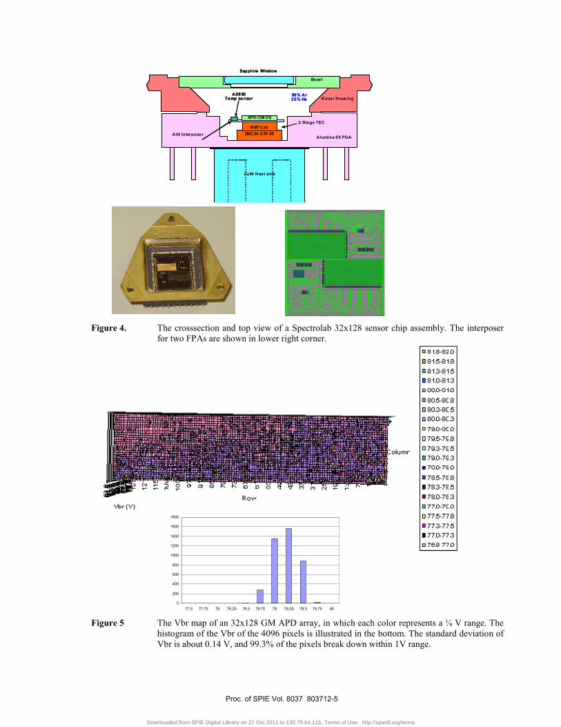
Figure 4. The crosssection and top view of a Spectrolab 32x128 sensor chip assembly. The interposer
for two FPAs are shown in lower right corner.
Bezel
Alumina 69 PGAAIN Interposer
Kovar Housing80% Ar20% He
Sapphire Window
AD590Temp sensor
CuW Heat sink
APD/CM OS
RMT Ltd2MC04-039-05
2-Stage TEC
Bezel
Alumina 69 PGAAIN Interposer
Kovar Housing80% Ar20% He
Sapphire Window
AD590Temp sensor
CuW Heat sink
APD/CM OS
RMT Ltd2MC04-039-05
2-Stage TEC
0
200
400
600
800
1000
1200
1400
1600
1800
77.5 77.75 78 78.25 78.5 78.75 79 79.25 79.5 79.75 80
Figure 5 The Vbr map of an 32x128 GM APD array, in which each color represents a ¼ V range. The histogram of the Vbr of the 4096 pixels is illustrated in the bottom. The standard deviation of Vbr is about 0.14 V, and 99.3% of the pixels break down within 1V range.
Proc. of SPIE Vol. 8037 803712-5
Downloaded from SPIE Digital Library on 27 Oct 2011 to 130.76.64.116. Terms of Use: http://spiedl.org/terms
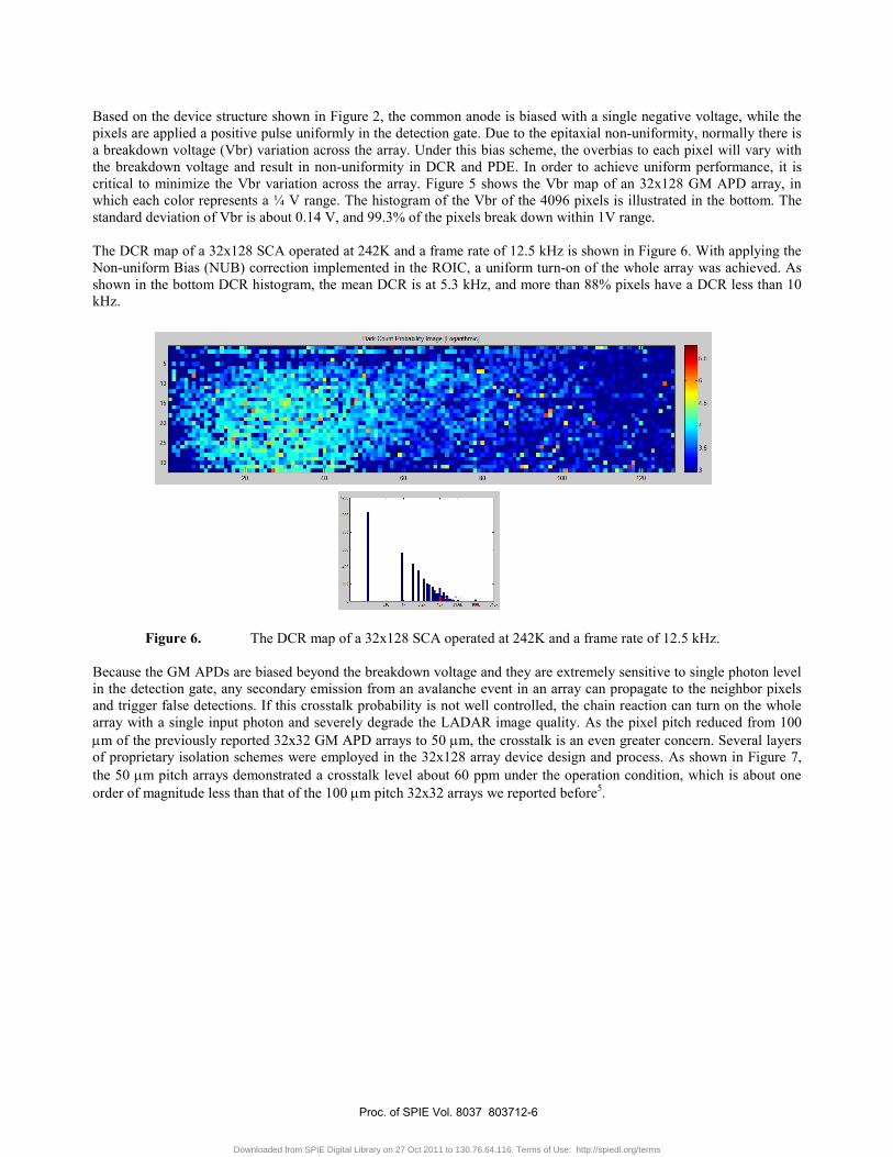
Based on the device structure shown in Figure 2, the common anode is biased with a single negative voltage, while the pixels are applied a positive pulse uniformly in the detection gate. Due to the epitaxial non-uniformity, normally there is a breakdown voltage (Vbr) variation across the array. Under this bias scheme, the overbias to each pixel will vary with the breakdown voltage and result in non-uniformity in DCR and PDE. In order to achieve uniform performance, it is critical to minimize the Vbr variation across the array. Figure 5 shows the Vbr map of an 32x128 GM APD array, in which each color represents a ¼ V range. The histogram of the Vbr of the 4096 pixels is illustrated in the bottom. The standard deviation of Vbr is about 0.14 V, and 99.3% of the pixels break down within 1V range. The DCR map of a 32x128 SCA operated at 242K and a frame rate of 12.5 kHz is shown in Figure 6. With applying the Non-uniform Bias (NUB) correction implemented in the ROIC, a uniform turn-on of the whole array was achieved. As shown in the bottom DCR histogram, the mean DCR is at 5.3 kHz, and more than 88% pixels have a DCR less than 10 kHz.
Figure 6. The DCR map of a 32x128 SCA operated at 242K and a frame rate of 12.5 kHz. Because the GM APDs are biased beyond the breakdown voltage and they are extremely sensitive to single photon level in the detection gate, any secondary emission from an avalanche event in an array can propagate to the neighbor pixels and trigger false detections. If this crosstalk probability is not well controlled, the chain reaction can turn on the whole array with a single input photon and severely degrade the LADAR image quality. As the pixel pitch reduced from 100 μm of the previously reported 32x32 GM APD arrays to 50 μm, the crosstalk is an even greater concern. Several layers of proprietary isolation schemes were employed in the 32x128 array device design and process. As shown in Figure 7, the 50 μm pitch arrays demonstrated a crosstalk level about 60 ppm under the operation condition, which is about one order of magnitude less than that of the 100 μm pitch 32x32 arrays we reported before5.
Proc. of SPIE Vol. 8037 803712-6
Downloaded from SPIE Digital Library on 27 Oct 2011 to 130.76.64.116. Terms of Use: http://spiedl.org/terms
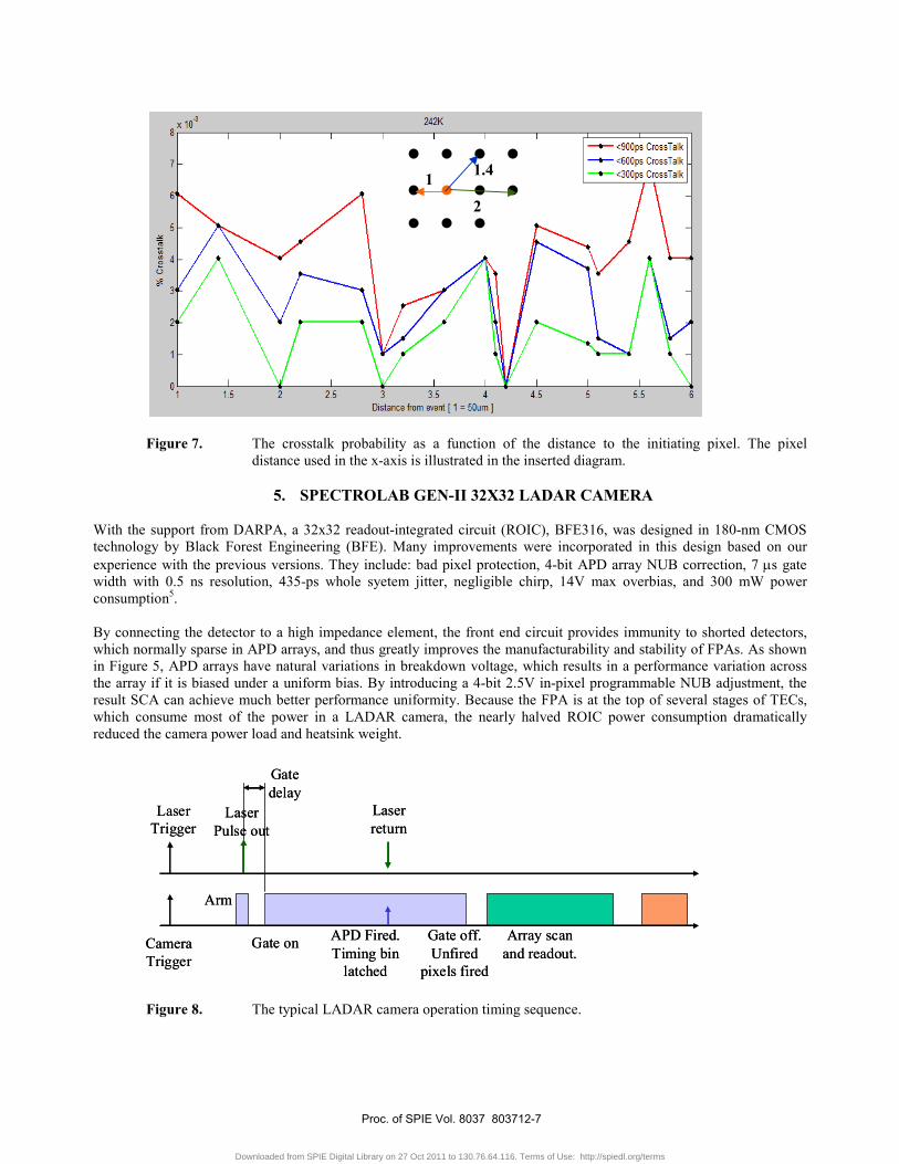
Figure 7. The crosstalk probability as a function of the distance to the initiating pixel. The pixel
distance used in the x-axis is illustrated in the inserted diagram.
5. SPECTROLAB GEN-II 32X32 LADAR CAMERA With the support from DARPA, a 32x32 readout-integrated circuit (ROIC), BFE316, was designed in 180-nm CMOS technology by Black Forest Engineering (BFE). Many improvements were incorporated in this design based on our experience with the previous versions. They include: bad pixel protection, 4-bit APD array NUB correction, 7 μs gate width with 0.5 ns resolution, 435-ps whole syetem jitter, negligible chirp, 14V max overbias, and 300 mW power consumption5. By connecting the detector to a high impedance element, the front end circuit provides immunity to shorted detectors, which normally sparse in APD arrays, and thus greatly improves the manufacturability and stability of FPAs. As shown in Figure 5, APD arrays have natural variations in breakdown voltage, which results in a performance variation across the array if it is biased under a uniform bias. By introducing a 4-bit 2.5V in-pixel programmable NUB adjustment, the result SCA can achieve much better performance uniformity. Because the FPA is at the top of several stages of TECs, which consume most of the power in a LADAR camera, the nearly halved ROIC power consumption dramatically reduced the camera power load and heatsink weight.
Figure 8. The typical LADAR camera operation timing sequence.
CameraTrigger
LaserTrigger
LaserPulse out
Arm
Gate on Gate off. Unfired
pixels fired
Gatedelay
Laserreturn
APD Fired. Timing bin
latched
Array scan and readout.
CameraTrigger
LaserTrigger
LaserPulse out
Arm
Gate on Gate off. Unfired
pixels fired
Gatedelay
Laserreturn
APD Fired. Timing bin
latched
Array scan and readout.
1
2
1.4
Proc. of SPIE Vol. 8037 803712-7
Downloaded from SPIE Digital Library on 27 Oct 2011 to 130.76.64.116. Terms of Use: http://spiedl.org/terms
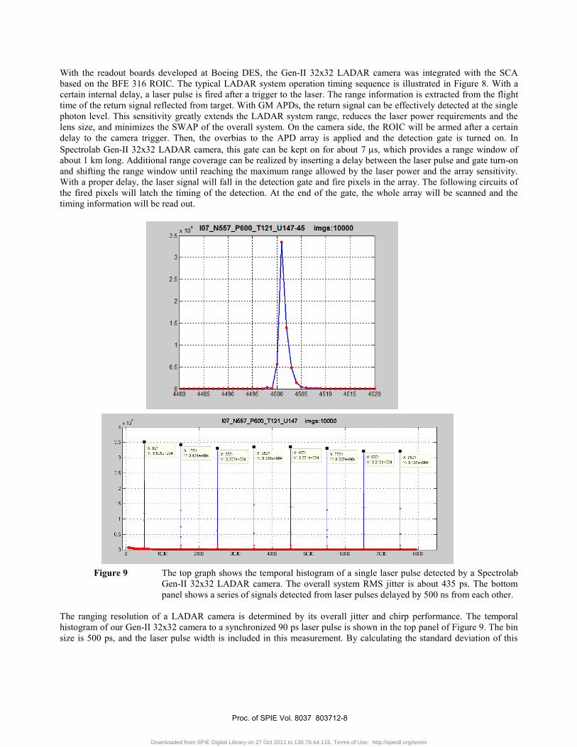
With the readout boards developed at Boeing DES, the Gen-II 32x32 LADAR camera was integrated with the SCA based on the BFE 316 ROIC. The typical LADAR system operation timing sequence is illustrated in Figure 8. With a certain internal delay, a laser pulse is fired after a trigger to the laser. The range information is extracted from the flight time of the return signal reflected from target. With GM APDs, the return signal can be effectively detected at the single photon level. This sensitivity greatly extends the LADAR system range, reduces the laser power requirements and the lens size, and minimizes the SWAP of the overall system. On the camera side, the ROIC will be armed after a certain delay to the camera trigger. Then, the overbias to the APD array is applied and the detection gate is turned on. In Spectrolab Gen-II 32x32 LADAR camera, this gate can be kept on for about 7 μs, which provides a range window of about 1 km long. Additional range coverage can be realized by inserting a delay between the laser pulse and gate turn-on and shifting the range window until reaching the maximum range allowed by the laser power and the array sensitivity. With a proper delay, the laser signal will fall in the detection gate and fire pixels in the array. The following circuits of the fired pixels will latch the timing of the detection. At the end of the gate, the whole array will be scanned and the timing information will be read out.
Figure 9 The top graph shows the temporal histogram of a single laser pulse detected by a Spectrolab
Gen-II 32x32 LADAR camera. The overall system RMS jitter is about 435 ps. The bottom panel shows a series of signals detected from laser pulses delayed by 500 ns from each other.
The ranging resolution of a LADAR camera is determined by its overall jitter and chirp performance. The temporal histogram of our Gen-II 32x32 camera to a synchronized 90 ps laser pulse is shown in the top panel of Figure 9. The bin size is 500 ps, and the laser pulse width is included in this measurement. By calculating the standard deviation of this
Proc. of SPIE Vol. 8037 803712-8
Downloaded from SPIE Digital Library on 27 Oct 2011 to 130.76.64.116. Terms of Use: http://spiedl.org/terms
temporal distribution, we can get the overall system RMS jitter of 435 ps, which includes the laser pulse width and jitters in the trigger loop, APDs, ROIC, and readout boards. With a new clock design, the chirp in this camera is negligible. As shown in the bottom panel of Figure 9, by increasing the delay of a laser pulse 500 ns each time, we have got a series of evenly spaced signals in the detection gate.
Figure 10. Photon counting LADAR system integrated with the Spectrolab Gen-II LADAR camera by
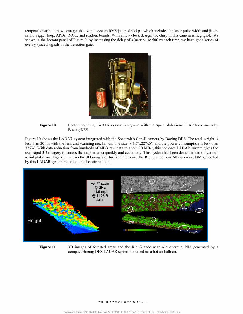
Boeing DES. Figure 10 shows the LADAR system integrated with the Spectrolab Gen-II camera by Boeing DES. The total weight is less than 20 lbs with the lens and scanning mechanics. The size is 7.5”x22”x6”, and the power consumption is less than 325W. With data reduction from hundreds of MB/s raw data to about 20 MB/s, this compact LADAR system gives the user rapid 3D imagery to access the mapped area quickly and accurately. This system has been demonstrated on various aerial platforms. Figure 11 shows the 3D images of forested areas and the Rio Grande near Albuquerque, NM generated by this LADAR system mounted on a hot air balloon.
Figure 11 3D images of forested areas and the Rio Grande near Albuquerque, NM generated by a
compact Boeing DES LADAR system mounted on a hot air balloon.
+/- 7° scan
@ 2Hz 11.5 mph @ 1125 ft
AGL
H i ht
Height
Proc. of SPIE Vol. 8037 803712-9
Downloaded from SPIE Digital Library on 27 Oct 2011 to 130.76.64.116. Terms of Use: http://spiedl.org/terms
To answer the challenges of SWIR LADAR applications, Spectrolab, teamed with Boeing DES and Black Forest Engineering, has been developing 32x128 GM-APD SCA and Gen-II LADAR camera. LADAR SCA performance has been greatly improved due to the continuous effect in materials, device design. Black Forest Engineering has designed and tested a new 32x32 ROIC loaded with many new functions and improved performance. The integration effort at Boeing DES made the cameras convenient to operate and commercially available. A compact LADAR system based on the new 32x32 camera was demonstrated on various platforms. With the 32x128 LADAR SCA developed under the DARPA program, the Spectrolab, Black Forest Engineering, and Boeing DES team, is developing the next generation GM APD 128x32 LADAR camera for SWIR applications.
ACKNOWLEDGEMENTS We would like to acknowledge the invaluable assistance provided by MIT Lincoln Laboratory over the last several years under various technology transfer programs. This effort has been funded under Boeing Whitespace program and DARPA Elusive Surface Target Engagement Technology contract HR0011-08-C-0020 under the direction of Dr. Monte Turner.
REFERENCES 1 K. A. McIntosh, et al., “Arrays of III-V semiconductor Geiger-mode avalanche photodiodes,” Lasers and Electro-
Optics Society, 2003. LEOS 2003. The 16th Annual Meeting of the IEEE. Volume 2, 686 (2003). 2 R. Sudharsanan, et al., “Single photon counting Geiger Mode InGaAs(P)/InP avalanche photodiode arrays for 3D
imaging,” Proc. SPIE 6950, 69500N (2008). 3 S. Verghese, et al., “Arrays of InP-based Avalanche Photodiodes for Photon Counting,” IEEE J. Selected Topics in
Quantum Electronics, 13, 870 (2007). 4 P. Yuan, et al., “High-performance InP Geiger-mode SWIR avalanche photodiodes,”, SPIE Defense, Security, and
Sensing, Advanced Photon Counting Techniques III. Proc. SPIE 7320, 73200P (2009). 5 P. Yuan, et al., “32 x 32 Geiger-mode LADAR cameras,” SPIE Defense, Security, and Sensing, Laser Radar
Technology and Applications XV. Proc. SPIE 7684, 76840C (2010).
6. SUMMARY
Proc. of SPIE Vol. 8037 803712-10
Downloaded from SPIE Digital Library on 27 Oct 2011 to 130.76.64.116. Terms of Use: http://spiedl.org/terms