general description digital versatile disc
TRANSCRIPT

GB 230-90347.911
LOEWE. DVD-PlayerXemixArt.-Nr. 59501
LOEWE systems DVD-PlayerAuroArt.-Nr. 59502
General DescriptionAdjustment ProceduresBlock / Schematic DiagramsExploded Views / Parts List
Digital Versatile Disc
CLASS 1LASER PRODUCT
TRACKTITLESCANTIMETRACKTOTAL
CHAPTERVCD SHUFFLECHAPTERTITLE TRACK
A -B REPEATFTS
TRACKTITLESCANTIMETRACKTOTAL
CHAPTERVCD SHUFFLECHAPTERTITLE TRACK
A -B REPEATFTS

Technical specificationsGB 2 59502 & 595011.
1. Technical specifications
1.1 General:
Mains voltage : 230V (196 - 263V AC)Mains frequency : 50 Hz -60HzPower consumption : 20WPower consumption standby : <10W (≤5W for low
power standby; without P50)
1.2 Audio performance
Test equipment : Audio PrecisionTestdiscs : CDDA: Philips audio
signal testdisc 1: VCD: Philips A/V
testdisc & ABEX A/V testdisc
: DVD: Philips LVP09.00 audio testdisc
1.3 Line output
1.3.1 'Normal' mode (stereo)
Output voltage :2 channel mode : 2Vrms +/- 1.5dB5.1 channel Dolby : 1.41 +/- 1.5 dBChannel unbalance (1kHz) : <0.85dBCrosstalk :1kHz : >105dB 20Hz-20kHz : > 95dBFrequency response :20Hz- 12kHz : +/- 0.1dB maxSignal to noise ratio : >100 dBDynamic range :1kHz : >90dB20Hz-20kHz : >88dBDistortion and noise :1kHz : >90dB20Hz-20kHz : >80dBIntermodulation distortion : >87dBPhase non linearity : +/- 1° max.Level non linearity : +/- 0.5dB max.Mute (spin-up, pause, access) : >100dBOutband attenuation : > 50dB above 25kHz
1.3.2 'Center on' mode (mono)
Output voltage : 2Vrms typChannel unbalance (1kHz : <0.85dBCrosstalk: : monoFrequency response(20Hz- 12kHz) : 0.1dB maxSignal to noise ratio : >85 dBDynamic range 20Hz-20kHz : >85 dBDistortion and noise 20Hz-20kHz : >80 dBIntermodulation distortion : >87 dBPhase non linearity : not applicableLevel non linearity : +/- 1 dBMute (spin-up, pause, access) : >100dBOutband attenuation : > 50dB above 25kHzCenterdelay adjusting : 0-5 msec (steps 1
msec)
1.4 6-channel output
1.4.1 Front Line out(channel 1 and 2)
fully according to PQR class IIIOutput voltage :channel mode : 1.41Vrms +/- 1.5dB5.1 channel Dolby : 1.41V +/- 1.5 dBChannel unbalance (1kHz) : <0.85dBCrosstalk :1kHz : >105dB20Hz-20kHz : > 95dBFrequency response 20Hz- 12kHz : +/- 0.1dB maxSignal to noise ratio : >100 dBDynamic range :1kHz : >90dB20Hz-20kHz : >88dBDistortion and noise :1kHz : >90dB20Hz-20kHz : >80dBIntermodulation distortion : >87dBPhase non linearity : +/- 1° max.Level non linearity : +/- 0.5dB max.Mute (spin-up, pause, access) : >100dBOutband attenuation : > 50dB above 25kHz
1.4.2 Surround channels (channel 3,4,5 and 6)
Surround channels are according to dolby group C products (*1)Testequipment: audio precision (*2)LFE + Center + Rear line out Output voltage :2 channel mode : muted5.1 channel Dolby : 1.41Vrms +/-1.5dB
: Adjustable 0.7V-2.82 V
: (+/- 6dB to front channels)
Channel unbalance : <0.85 dBSignal to noise ratio : >100 dB (A-weighted)Dynamic range : >85 dBDistortion and noise : >80 dB (90 typical)Crosstalk: : >95 dB (*3)*1 : referenced to dolby
digital licensee information manual version 2.0
*2 : measured in normal mode and with balance control neutral
*3 : crosstalk from channels 1,3,5(channel 1 is ref) to 2,4,6(measured channels)
1.5 Headphone output
According PQR1 IMS30mW at 32 Ohm load.Headphone impedance: 8-2000 Ohm
1.6 Video performance VCD testdisc : Philips A/V disc & ABEX A/V disc

Technical specifications GB 359502 & 59501 1.
DVD testdisc : Philips MPTD PAL CVP0213 / Philips LVP10.00 video testdisc
1.6.1 CVBS
Fully according PQR3 IMSVideo output : 1Vpp(0.1V into 75
Ohm)
1.6.2 S-video (Y/C)
Fully according PQR3 IMS1 - GND
2 - GND
3 - Y 1Vpp +/- 0.1V into 75 Ohm 4 - C burst 300mVpp +1/-4dB into 75
Ohm Aspect ratio switching by DC on C(pin4).Connector type : 4 pin mini- DIN
1.7 Scart
Fully according PQR3 IMSConnector implementation according EN50049-1; color = black; dual SCARTFully according to prEN1057-2-1Signal switching is P50 controlled; supported features of mode 3 see survey of applicable standards.
1.7.1 SCART II (connected to TV)
Pin signals:1 - Audio R 1.8V RMS
2 - Audio R
3 - Audio L 1.8V RMS
4 - Audio GND
5 - Blue/Chroma GND
6 - Audio L
7 - Blue out/Chroma in 0.7Vpp +/- 0.1V into 75 Ohm (*)
8 - Function switch <2V = TV
>4.5V / <7V = asp. ratio 16:9 DVD>9.5V / <12V = asp. ratio 4:3 DVD
9 - Green GND
10- Nc 11- Green 0.7Vpp +/- 0.1V into 75 Ohm (*)
12- Nc 13- Red/Chroma GND
14- Fast switch GND
15- Red out/Chroma out 0.7Vpp +/- 0.1V into 75 Ohm (*)
+/- 3dB 0.3Vpp in case of Chroma
16- Fast switch RGB/ CVBS or Y <0.4V into 75 Ohm = CVBS
>1V / <3V into 75 Ohm = RGB
17- Y/CVBS GND
18- Fast switching GND
19- CVBS/Y/RGB sync 1Vpp +/- 0.1V into 75 Ohm (*)
20- CVBS/Y
21- Shield
1.7.2 SCART I (connected to AUX)
Pin signals:1 - Audio R 1.8V RMS
2 - Audio R
3 - Audio L 1.8V RMS
4 - Audio GND
5 - Blue/Chroma GND
6 - Audio L
7 - Blue in/Chroma out +/- 3dB 0.3vpp Chroma (burst)
8 - Function switch
9 - Green GND
10- P50 Control 11- Green
12- Nc 13- Red/Chroma GND
14- Fast switch GND
15- Red in/Chroma in
16- Fast switch RGB/ CVBS or Y
17- CVBS GND
18- Fast switching GND
19- CVBS/Y/RGB sync 1Vpp +/- 0.1V into 75 Ohm (*)
20- CVBS/Y
21- Shield
(*) for 100% white
1.8 Digital output
1.8.1 Coaxial
CDDA/ LPCM (incl MPEG1) : According IEC958MPEG2, AC3 audio : According IEC1937Remark:DTS audio output mode is only available on “digital out”
1.8.2 Optical
Identical to coaxial
1.9 Dimensions and weight
Place and height of feet : acc. to Loewe Harmonisation line
Apparatus tray closed : WxDxH: 435 x 315x 75/88
Apparatus tray open : WxDxH: 435 x 442 x 75/88
Weight without packaging : ca. 4 KgWeight in packaging : ca. 6 Kg
1.10 Laser output power & wavelength
1.10.1 DVD
Output power : 7mWWavelength : 650nm
1.10.2 CD
Output power : 10mWWavelength : 785nm
Warnings and Laser safety instructionsGB 4 59502 & 595012.
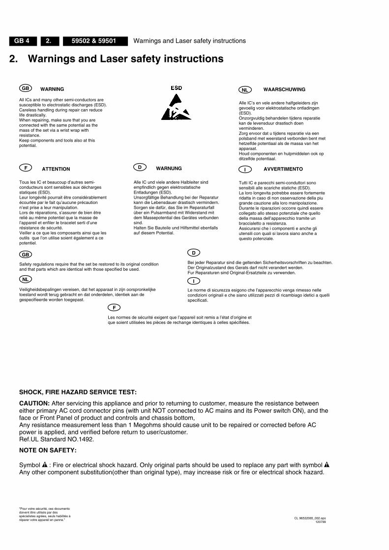
2. Warnings and Laser safety instructions
SHOCK, FIRE HAZARD SERVICE TEST:
CAUTION: After servicing this appliance and prior to returning to customer, measure the resistance betweeneither primary AC cord connector pins (with unit NOT connected to AC mains and its Power switch ON), and theface or Front Panel of product and controls and chassis bottom,Any resistance measurement less than 1 Megohms should cause unit to be repaired or corrected before ACpower is applied, and verified before return to user/customer.Ref.UL Standard NO.1492.
NOTE ON SAFETY:
Symbol : Fire or electrical shock hazard. Only original parts should be used to replace any part with symbol Any other component substitution(other than original type), may increase risk or fire or electrical shock hazard.
F ATTENTION
Tous les IC et beaucoup d’autres semi-conducteurs sont sensibles aux déchargesstatiques (ESD).Leur longévité pourrait être considérablementécourtée par le fait qu’aucune précautionn’est prise a leur manipulation.Lors de réparations, s’assurer de bien êtrerelié au même potentiel que la masse del’appareil et enfiler le bracelet serti d’unerésistance de sécurité.Veiller a ce que les composants ainsi que lesoutils que l’on utilise soient également a cepotentiel.
D WARNUNG
Alle IC und viele andere Halbleiter sindempfindlich gegen elektrostatischeEntladungen (ESD).Unsorgfältige Behandlung bei der Reparaturkann die Lebensdauer drastisch vermindern.Sorgen sie dafür, das Sie im Reparaturfallüber ein Pulsarmband mit Widerstand mitdem Massepotential des Gerätes verbundensind.Halten Sie Bauteile und Hilfsmittel ebenfallsauf diesem Potential.
WAARSCHUWING
Alle IC’s en vele andere halfgeleiders zijngevoelig voor elektrostatische ontladingen(ESD).Onzorgvuldig behandelen tijdens reparatiekan de levensduur drastisch doenverminderen.Zorg ervoor dat u tijdens reparatie via eenpolsband met weerstand verbonden bent methetzelfde potentiaal als de massa van hetapparaat.Houd componenten en hulpmiddelen ook opditzelfde potentiaal.
AVVERTIMENTO
Tutti IC e parecchi semi-conduttori sonosensibili alle scariche statiche (ESD).La loro longevita potrebbe essere fortementeridatta in caso di non osservazione della piugrande cauzione alla loro manipolazione.Durante le riparazioni occorre quindi esserecollegato allo stesso potenziale che quellodella massa dell’apparecchio tramite unbraccialetto a resistenza.Assicurarsi che i componenti e anche gliutensili con quali si lavora siano anche aquesto potenziale.
All ICs and many other semi-conductors aresusceptible to electrostatic discharges (ESD).Careless handling during repair can reducelife drastically.When repairing, make sure that you areconnected with the same potential as themass of the set via a wrist wrap withresistance.Keep components and tools also at thispotential.
WARNING
Safety regulations require that the set be restored to its original conditionand that parts which are identical with those specified be used.
Veiligheidsbepalingen vereisen, dat het apparaat in zijn oorspronkelijketoestand wordt terug gebracht en dat onderdelen, identiek aan degespecifieerde worden toegepast.
Bei jeder Reparatur sind die geltenden Sicherheitsvorschriften zu beachten.Der Originalzustand des Gerats darf nicht verandert werden.Fur Reparaturen sind Original-Ersatzteile zu verwenden.
Le norme di sicurezza esigono che l’apparecchio venga rimesso nellecondizioni originali e che siano utilizzati pezzi di ricambiago idetici a quellispecificati.
Les normes de sécurité exigent que l’appareil soit remis a l’état d’origine etque soient utilisées les pièces de rechange identiques à celles spécifiées.
“Pour votre sécurité, ces documentsdoivent être utilisés par desspécialistes agrées, seuls habilités àréparer votre appareil en panne.”
GB NL
I
D
I
F
GB
NL
CL 96532065_002.eps120799

Warnings and Laser safety instructions GB 559502 & 59501 2.
LASER SAFETY
This unit employs a laser. Only a qualified service person should remove the cover or attempt to service thisdevice, due to possible eye injury.
LASER DEVICE UNIT
Type: Semiconductor laser GaAlAsWave length: 650 nm (DVD)
780 nm (VCD/CD)Output Power: 7 mW (DVD)
10 mW (VCD/CD)Beam divergence: 60 degree
USE OF CONTROLS OR ADJUSTMENTS OR PERFORMANCE OF PROCEDURE OTHER THAN THOSESPECIFIED HEREIN MAY RESULT IN HAZARDOUS RADIATION EXPOSURE.
AVOID DIRECT EXPOSURE TO BEAM
WARNING
The use of optical instruments with this product will increase eye hazard.Repair handling should take place as much as possible with a disc loaded inside the player
WARNING LOCATION: INSIDE ON LASER COVERSHIELD
CAUTION VISIBLE AND INVISIBLE LASER RADIATION WHEN OPEN AVOID EXPOSURE TO BEAM ADVARSEL SYNLIG OG USYNLIG LASERSTRÅLING VED ÅBNING UNDGÅ UDSÆTTELSE FOR STRÅLING ADVARSEL SYNLIG OG USYNLIG LASERSTRÅLING NÅR DEKSEL ÅPNES UNNGÅ EKSPONERING FOR STRÅLEN VARNING SYNLIG OCH OSYNLIG LASERSTRÅLNING NÄR DENNA DEL ÄR ÖPPNAD BETRAKTA EJ STRÅLEN VARO! AVATT AESSA OLET ALTTIINA NÄKYVÄLLE JA NÄKYMÄTTÖMÄLLE LASER SÄTEILYLLE. ÄLÄ KATSO SÄTEESEEN VORSICHT SICHTBARE UND UNSICHTBARE LASERSTRAHLUNG WENN ABDECKUNG GEÖFFNET NICHT DEM STRAHL AUSSETZEN DANGER VISIBLE AND INVISIBLE LASER RADIATION WHEN OPEN AVOID DIRECT EXPOSURE TO BEAM ATTENTION RAYO NNEMENT LASER VISIBLE ET INVISIBLE EN CAS D'OUVERTURE EXPOSITION DANGEREUSE AU FAISCEAU
Warning for powersupply on position 1005
The primary side of the powersupply including the heatsink carries live mains voltage when theplayer is connected to the mains even when the player is swiched off !This primary area is not shielded so it is possible to touch copper tracks and/or components whenservicing the player. Service personnel have to take precautions to prevent touching this area orcomponents in this area .The primary side of the powersupply has been indicated with a lightning stroke and a stripe-markedprinted on the printed wiring board
Note:The screws on the basic Engine (position 82 in on the exploded view drawing) may never betouched removed or re-adjusted.Handle the Basic engine with care when the unit has to be exchanged!The mechanism of the basic engine is very sensative for droping or shocks
!
CL 96532065_003.eps011199

Service hintsGB 6 59502 & 595013.
3. Service hints
The DVD module(Basic Engine and the mono board) has to be exchanged completely in case of failure. A new module for Xemixcan be ordered with codenumber 291-90350.969 for Region Code 4 (Australia), 291-90350.970 for Region Code 5 (Russia), and 291-90350.968 for all European countries Region Code 2.A new module for Auro can be ordered with codenumber 291-90350.988 for Region Code 4 (Australia), 291-90350.989 for Region Code 5 (Russia),and 291-90350.987 for all European countries Region Code 2. Return the defective unit complete assembled in original package to Loewe Consumer Service in Kronach.

DIAGNOSTIC SOFTWARE : SCRIPT INTERFACES GB 2759502 & 59501 6.
6. DIAGNOSTIC SOFTWARE : SCRIPT INTERFACES
6.1 DEALER SCRIPT
6.1.1 Purpose of Dealer Script
The dealer script can give a diagnosis on a standalone DVD player; no other equipment is needed to perform a number of hardware tests to check if the DVD player is faulty. The diagnosis is simply a "error" or "pass" message; no indication is given of faulty hardware modules. Only tests within the scope of the diagnostic software will be executed hence only faults within this scope can be detected.
6.1.2 Contents of Dealer Script
The dealer script executes all diagnostic nuclei that do not need any user interaction and are meaningful on a standalone DVD player.The nuclei called in the dealer script are the following (the number after each nucleus name corresponds with the number being on the local display when the nucleus is executed during the dealer script):
Figure 6-1
Figure 6-2
VideoColSetupComm Checks the I2C interface with the RGB video processor on theAudio/Video board (only for DVD players with RGB video processor).
VideoScartSwComm Checks the I2C interface with the scart switch on the Audio/Videoboard
PapChksFl 7 Calculate and verify checksum of FLASH memory.PapDramWrR 6 Pattern test of all locations in the DRAM(s).PapI2cDisp Checks the I2C interface with the slave processor on the display PCB.PapS2bEcho Checks the I2C interface to the basic engine.PapI2cNvram Checks the I2C interface with the NVRAM.PapNvramWrR Pattern test of all locations in the NVRAMCompSdramWrR Pattern test of all locations in the SDRAM(s).
Nucleus
8
5
4
3
2
1
9
Description
CL 96532065_001.eps120799
Press 2 keys simultaneously<OPEN/CLOSE> + <PAUSE>
Connect to mains.
During the test, the following displayis shown: the counter counts downfrom the number of nuclei to be runbefore the test finishes. Example:
SET O.K.?
YES
NO
To exit DEALER SCRIPT ,disconnect from mains.
CL96532126_013.eps261099

DIAGNOSTIC SOFTWARE : SCRIPT INTERFACESGB 28 59502 & 595016.
6.2 PLAYER SCRIPT
6.2.1 Purpose of Player Script
The Player script will give the opportunity to perform a test that will determine which of the DVD player's modules are faulty, to read the error log and error bits and to perform an endurance loop test. To successfully perform the tests, the DVD player must be connected to a tv set to check the output of a number of nuclei. For DVDv2b a multi-channel amplifier, a set of 6 boxes and an external video source are necessary to test. To be able to check results of certain nuclei, the player script expects some interaction of the user (i.e. to approve a test picture or a test sound). Some nuclei (e.g. nuclei that test functionality of the Basic Engine module) require that the DVD player itself is opened, to enable the user to observe moving parts and approve their movement visually. Only tests within the scope of the diagnostic software will be executed hence only faults within this scope can be detected.
6.2.2 Contents of Player Script
The player script contains all nuclei that are useful on a DVD player that is connected to a tv-set and help to determine which module of the DVD player is faulty, as well as to read out the contents of the error logs.
6.2.3 Structure of Player Script
The player script consists of a set of nuclei testing the three hardware modules in the DVD player: the Display PWB, the Digital PWB and the Basic Engine.Nuclei run by the player test need some user interaction; in the next paragraph this interaction is described. The player test is done in two phases:1. Interactive tests: this part of the player test depends
strongly on user interaction and input to determine nucleus results and to progress through the full test. Reading the error log and error bits information can be useful to determine any errors that occurred recently during normal operation of the DVD player.
2. The loop test will perform the same nuclei as the dealer test, but it will loop through the list of nuclei indefinitely.
6.2.4 Survey
Figure 6-3
SLEDGE TEST BeSledgeOut/In(41ab)
FOCUS TEST BeFocusOn(38a)
DISC MOTOR TEST BeDiscMotorOn(39a)
RADIAL TEST BeRadialOn(40a)
JUMP TEST BeGroovesIn/Mid/Out(42abc)
Press 2 keys simultaneously<OPEN/CLOSE> + <STOP>
Connect to mains
To exit player test,disconnect from mains
INTERACTIVE TESTS
DISPLAY TEST DispDisplay(30)
LED TEST DispLed(29)
KEYBOARD TEST DispKeyb(27)
SCART LOOP TEST
AudioPinkNoiseOn(20a)VideoScartSwDvd(54a)
VideoColDencOn(23a)PICTURE TEST
DISPLAY PCB
MONO PCB(SERVO)& BASIC ENGINE
MONO PCB(DIGITAL)AUDIO/VIDEO PCB
TRAY TEST BeTrayOut/In(43ab)
VERSION NUMBER BeVer(37)
REMOTE CONTROL DispRc(28)
TRAY TEST BeTrayOut/In(43ab)
ERROR LOG & BITSLogReadErr(31) LogReadbits(32)
LOOP TEST = Dealer script exclusive of test2
AudioSineOn(21a)
VideoColSetupHi(53a)VideoColSetupLo(53b)
SOUND 1 TESTSCART DVD TEST
SOUND 2 TEST
COLOUR SETUP TEST
VideoScartSwPass(54b)
CL96532126_014.eps261099

DIAGNOSTIC SOFTWARE : SCRIPT INTERFACES GB 2959502 & 59501 6.
6.3 INTERACTIVE TESTS
6.3.1 DISPLAY PCB
DISPLAY TESTThe display test is performed by nucleus DispDisplay. By putting a series of test patterns on the local display, the local display is tested. To step through all different patterns, the user must either press PLAY (pattern is ok) or PAUSE (pattern was incorrect) to proceed to the next pattern. The display of patterns is continued in a cyclic manner until the user presses NEXT. If the user presses NEXT before all display patterns are tested, the DispDisplay nucleus will return TRUE (display test successful).
LED TESTThe LED(s) on the DVD player is (are) tested by nucleus DispLed. The user must check if the LED(s) is (are) lighted; if it is, press PLAY, if it is not, press PAUSE. By pressing NEXT the script will proceed to the next test. If the user presses NEXT before PLAY or PAUSE, the DispLed nucleus will return TRUE (LED test successful).
Figure 6-4
KEYBOARD TESTThe keyboard of the DVD player is tested by nucleus DispKeyb. The user is expected to press all keys on the local keyboard once. The code of the key pressed is shown on the local display (1 hexadecimal digit) immediately followed by a (hexadecimal) number indicating how many times that key has been pressed. Example of the local display during this test:
Figure 6-5
The key-codes displayed on the local display will scroll from right to left when the display gets full, the text "tb-" will remain on display.
Figure 6-6
If any keys are detected more than once (due to hardware error), the key-code is displayed twice (or more), with the second digit increased by 1. If the user does not press all keys minimally once (in any order), the DispKeys nucleus will return FALSE and cause an error in the overall result of the player script. The user can leave the keyboard test by pressing the NEXT key on the local display of the DVD player for at least one full second. The result of the keyboard test is shown on local display as follows:
Figure 6-7
Or
Figure 6-8
Pressing NEXT on the local keyboard again will proceed to the next text.
REMOTE CONTROL TESTThe remote control of the DVD player is tested by nucleus DispRc. The user must press any key on the remote control just once. The codes of the key pressed will be shown on the local display in hexadecimal format. Example:
Figure 6-9
In this example 23 is the hexidecimal code of the pressed RC key. The user can leave the remote-control test by pressing NEXT on the local keyboard of the DVD player. The remote control test is successful if a code was received before the user pressed the NEXT key; pressing the NEXT key before pressing a key on the remote control gives an error in the remote control
If OK, press PLAY If NOK, press PAUSE
If OK, press PLAY If NOK, press PAUSE
If OK, press PLAY If NOK, press PAUSE
press NEXT to continue CL 96532065_006.eps120799
CL 96532065_007.eps120799
key id. key0 PLAY1 NEXT2 PREVIOUS3 PAUSE4 STOP5 OPEN/CLOSE6 3D-SOUNDA STANDBY
CL96532126_015.eps261099
CL 96532065_009.eps120799
CL 96532065_010.eps120799
CL 96532065_011.eps120799

DIAGNOSTIC SOFTWARE : SCRIPT INTERFACESGB 30 59502 & 595016.
test (note that the remote control test will also fail if a key on the remote control was pressed but no code was received). The remote control test does not check upon the contents of the received code, that is it will not be checked if the received code matches the key pressed. If desired, the user can manually check this code by using a code-table for the remote control key-codes.
Figure 6-10
After pressing NEXT, the result of the remote control test is displayed on the local display of the DVD player as follows:
Figure 6-11
Or
Figure 6-12
Pressing NEXT on the local keyboard again will proceed to the next test.
6.3.2 MONO PCB DIGITAL PART
PICTURE TESTThe picture test is performed by putting a predefined picture (colour bar) on the display (nucleus VideoColDencOn) and asking the user for confirmation. The display will show the following message:
Figure 6-13
By pressing PLAY the user confirms the test, pressing PAUSE will indicate the picture was invisible or incorrect. Pressing NEXT will proceed to the next test
SOUND 1 & SCART DVD TESTThe first soundtest is performed by starting a pink noise sound that needs confirmation from the user (nucleus AudioPinkNoiseOn); the display will show the following message very shortly:
Figure 6-14
This sound will only be audible from version cut3.1 of Sti5505(item7503 on mono board) onwards. After starting up sound 1, SCART loop-trough will be simultaneously active during this test. SCART loop-trough will be measured with the aid of an external video source.When entering the SCART loop-trough, the local display indicates:
RC Key id Hexadecimal codeSTANDBY CSTOP 31PLAY 2CPLAY BACKWARD 2DPAUSE 30STEP FORWARD F6STEP BACKWARD F5FORWARD 28FORWARD 4X DFFORWARD 8X E0BACKWARD 29BACKWARD 4X DEBACKWARD 8X DDSLOW 22SLOW 2 D8SLOW BACKWARD 23SLOW BACKWARD 2 DBNEXT 20PREVIOUS 21CURSOR UP 58CURSOR DOWN 59CURSOR LEFT 5ACURSOR RIGHT 5BOK 5C0 01 12 23 34 45 56 67 78 89 9TOGGLE C8ANGLE 85AUDIO 4ESUBTITLES 4BSUBTITLE ON/OFF E3ROOT MENU 54TITLE MENU 71MENU D1SETUP MENU 82OSD ON/OFF FRETURN 83RESUME D7SCAN 2ASHUFFLE 1CREPEAT 1DA/B REPEAT 3DTOGGLE SCART 43OPEN/CLOSE 42FTS FBKARAOKE E4OPTION FA
CL 96532065_012.eps120799
CL 96532065_013.eps120799
CL 96532065_014.eps120799
CL 96532065_015.eps120799
CL 96532065_016.eps120799

DIAGNOSTIC SOFTWARE : SCRIPT INTERFACES GB 3159502 & 59501 6.
Figure 6-15
On the TV screen a colour bar (generated by nucleus VideoColDencOn) is visual and the internally generated pinknoise is audible. By pressing PLAY the user confirms the test, pressing PAUSE will indicate the sound was inaudible or incorrect. Pressing NEXT will proceed to the next test; if the user presses NEXT without pressing PLAY or PAUSE first, the result of this test will be TRUE (sound ok). By pressing the NEXT button there will be switched over to the external source, this must become now visible on the TV screen (using the SCART). The local display indicates:
Figure 6-16
The internally generated colour bar is still available on the CVBS and Y/C outputs. And the pinknoise-signal is still available on the cinch audio outputs. By pressing the PREV button, the internal generated colour bar becomes visual again. The test can be left by pressing the NEXT key for more than one second.
SOUND 2 TESTThe second soundtest is performed by producing a sine sound (nucleus AudioSineOn). The signal can be stopped by pressing the STOP-key. The display will show the following message:
Figure 6-17
By pressing PLAY the user confirms the test, pressing PAUSE will indicate that something went wrong. Pressing NEXT will proceed to the next; if the user presses NEXT without pressing PLAY or PAUSE first, the result of this test will be TRUE (sound ok).
Colour set-up testThe colour set-up test is performed by putting the internally generated colour bar in diffferent settings on the TV screen. The first colour bar will be displayed in setting 1. The display will show the following message:
Figure 6-18
By pressing the NEXT button, you can go to the second setting. The local display indicates:
Figure 6-19
By pressing the PREVIOUS button, the colour bar with the first setting becomes visual again.By pressing PLAY the user confirms the test, pressing PAUSE will indicate that something went wrong. The test can be left by pressing the NEXT key for more than one second; if the user presses NEXT without pressing PLAY or PAUSE first, the result of this test will be TRUE (colour set-up ok).
6.3.3 BASIC ENGINE
VERSION NUMBERIn the basic engine tests, the version number of the Basic Engine will be shown first, as the following example:
Figure 6-20
By pressing the NEXT key, the Basic Engine tests are started.
TRAY TESTFirst, the tray is tested. The purpose of this test is also to give the user the opportunity to put a disc in the tray of the DVD player. Some tests on the Basic Engine require that a disc(e.g. DVD MPTD test disc) is present in the player. At the end of the Basic Engine tests this tray test will be repeated solely to enable the user to remove the disc in the tray. The local display will look as follows:
Figure 6-21
By pressing PLAY or PAUSE the user can toggle the position of the tray. Note that this test will not contribute to the test result of the Basic Engine. Pressing NEXT will proceed to the next test, after the tray has been closed (by the software) if it was open.
SLEDGE TEST(visual test)The second Basic Engine test tests the sledge; the user can move the sledge as many times as desired by using PLAY (nucleus BeSledgeOut) and PAUSE (nucleus BeSledgeIn). Pressing NEXT on the local keyboard proceeds to the next test. Note that this test will not contribute to the test result of the Basic Engine. The local display will look as follows during the sledge test:
CL 96532065_017.eps120799
CL 96532065_018.eps120799
CL 96532065_019.eps120799
CL96532126_016.eps261099
CL96532126_017.eps261099
CL96532126_018.eps261099
CL 96532065_021.eps120799

DIAGNOSTIC SOFTWARE : SCRIPT INTERFACESGB 32 59502 & 595016.
Figure 6-22
DISC MOTOR TEST(visual test)The third Basic Engine test tests the disc motor (nucleus BeDiscMotorOn); the local display looks as follows:
Figure 6-23
By pressing PLAY the user confirms that the disc motor is running; pressing PAUSE indicates the disc motor does not work. Pressing NEXT proceeds to the next test, after a reset of the disc motor (nucleus BeDiscMotorOff). If the user presses NEXT before pressing PLAY or PAUSE, the result of this test will be TRUE (disc motor is running).
FOCUS TEST(visual test)The fourth Basic Engine test tests the focussing; first focussing is turned on by calling nucleus BeFocusOn. The display will look as follows:
Figure 6-24
By pressing PLAY the user confirms that the focussing was succesful; pressing PAUSE indicates a focussing failure. Pressing NEXT proceeds to the next test after a reset of the focussing (nucleus BeFocusOff); if NEXT is pressed before PLAY or PAUSE, the result of this test will be TRUE (focus successful).
RADIAL TEST(visual & listening test)The fifth Basic Engine test tests the radial functionality (nucleus BeRadialOn); the local display looks as follows:
Figure 6-25
By pressing PLAY the user confirms that the radial function worked; pressing PAUSE indicates the function does not work. Pressing NEXT proceeds to the next test, after a reset of the radial (nucleus BeRadialOff). If the user presses NEXT before pressing PLAY or PAUSE, the result of this test will be TRUE (radial successful).
JUMP TEST(listening test)The sixth and last Basic Engine test tests the jumping by calling nuclei BeGroovesIn, BeGroovesMid and BeGroovesOut. During this test, the local display looks as follows:
Figure 6-26
The user can switch between the three different types of groove settings by pressing PLAY (forward to next nucleus in the list In-Mid-Out) or PAUSE (backward in the list In-Mid-Out). This is done in a cyclic manner; note that this test will not contribute to the test result of the Basic Engine. Pressing NEXT proceeds to the next test, after the disc motor has been shut off with a call to nucleus BeDiscMotorOff.
TRAY TESTAs a last action for the Basic Engine tests, the tray test is repeated. The local display will look as follows:
Figure 6-27
This test is meant to give the user the opportunity to remove the disc in the tray. The tray position can be toggled using the PLAY and PAUSE key. The tray will be closed (by the software, if it is open) before proceeding to the next test when the user presses the NEXT key.
CL 96532065_022.eps120799
CL 96532065_023.eps120799
CL 96532065_024.eps120799
CL 96532065_025.eps120799
CL 96532065_026.eps120799
CL 96532065_027.eps120799

DIAGNOSTIC SOFTWARE : SCRIPT INTERFACES GB 3359502 & 59501 6.
ERROR LOGReading the error log and error bits information can be useful to determine any errors that occurred recently during normal operation of the DVD player. Reading the error log is done by nucleus LogReadErr. The display during the errorlog readout looks as follows :
Figure 6-28
By pressing PLAY or PAUSE the user can move forward or backward (respectively) through the logged error codes. The highlighted number indicates which errorcode is currently on display (in the example above, errorcode number 4 is displayed). If "0000" is displayed at all positions, the error log is empty. Display of the logged errors is done in a cyclic manner. The errorcode with the lowest highlighted number is the most
recent. By pressing NEXT on the local keyboard, the user can proceed to the next test.
ERROR BITSReading the error bits is done by nucleus LogReadBits. The display during the errorbits readout looks as follows:
Figure 6-29
Only the set errorbits will be shown by their (decimal) number. Refer to the appropriate documentation for the explanation of each bit number. If the display only shows "EB-0", no error bits were set. By pressing NEXT the user can continue to the next test.See table below:
CL96532126_019.eps261099
CL96532126_020.eps261099
Error log / bits table Read ERROR LOG in player script
Read ERROR BITS in player script
Basic engine errors Value: Value:
Command to the Basic Engine not allowed in this stae or unknown command
150101 8
Parameter(s) from the command to the Basic Engine is not valid 150102 7
Sledge could not be moved to the ineer home position 150103 6
Focus failure 150104 5
Turntable motor could not be reached within timeout 150105 4
Radial servo could get on track on the disc 150106 3
PLL could not lock in the accessing or tracking state 150107 2
Subcode or sector information could not be read 150108 1
requested subcode could not be found 150109 16
Tray could not be closed or opened completely 15010A 15
TOC could not be read within timeout 15010B 14
The requested seek on the disc could not be executed 15010C 13
A requested lead is not on the disc 15010D 12
A non existing burst cutting area is requested 15010E 11
S2b communication error 1501F0 10
S2b communication error 1501F1 9
S2b communication error 1501F3 24
S2b communication error 1501F4 23
S2b communication error 1501F5 22
Digital PWB errors
Communication error with the Sti 5505 90000 32
Communication error with the Sti 5505 90001 31
Disply processor errors
Communication error with the display processor 190000 40
DIAGNOSTIC SOFTWARE : SCRIPT INTERFACESGB 34 59502 & 595016.
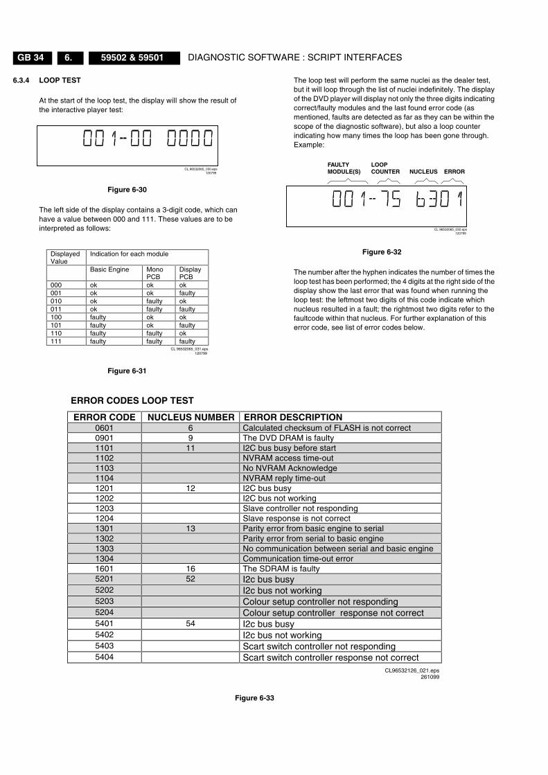
6.3.4 LOOP TEST
At the start of the loop test, the display will show the result of the interactive player test:
Figure 6-30
The left side of the display contains a 3-digit code, which can have a value between 000 and 111. These values are to be interpreted as follows:
Figure 6-31
The loop test will perform the same nuclei as the dealer test, but it will loop through the list of nuclei indefinitely. The display of the DVD player will display not only the three digits indicating correct/faulty modules and the last found error code (as mentioned, faults are detected as far as they can be within the scope of the diagnostic software), but also a loop counter indicating how many times the loop has been gone through. Example:
Figure 6-32
The number after the hyphen indicates the number of times the loop test has been performed; the 4 digits at the right side of the display show the last error that was found when running the loop test: the leftmost two digits of this code indicate which nucleus resulted in a fault; the rightmost two digits refer to the faultcode within that nucleus. For further explanation of this error code, see list of error codes below.
Figure 6-33
CL 96532065_030.eps120799
DisplayedValue
Indication for each module
Basic Engine MonoPCB
DisplayPCB
000 ok ok ok001 ok ok faulty010 ok faulty ok011 ok faulty faulty100 faulty ok ok101 faulty ok faulty110 faulty faulty ok111 faulty faulty faulty
CL 96532065_031.eps120799
FAULTYMODULE(S)
LOOPCOUNTER NUCLEUS ERROR
CL 96532065_032.eps120799
ERROR CODES LOOP TEST
ERROR CODE NUCLEUS NUMBER ERROR DESCRIPTION0601 6 Calculated checksum of FLASH is not correct0901 9 The DVD DRAM is faulty1101 11 I2C bus busy before start1102 NVRAM access time-out1103 No NVRAM Acknowledge1104 NVRAM reply time-out1201 12 I2C bus busy1202 I2C bus not working1203 Slave controller not responding1204 Slave response is not correct1301 13 Parity error from basic engine to serial1302 Parity error from serial to basic engine1303 No communication between serial and basic engine1304 Communication time-out error1601 16 The SDRAM is faulty5201 52 I2c bus busy5202 I2c bus not working5203 Colour setup controller not responding5204 Colour setup controller response not correct5401 54 I2c bus busy5402 I2c bus not working5403 Scart switch controller not responding5404 Scart switch controller response not correct
CL96532126_021.eps261099

Servicing DVD module and MONO board GB 3559502 & 59501 7.
7. Servicing DVD module and MONO board
7.1 Replacing DVD module
7.2 Reprogramming of new mono boards.
Figure 7-1
7.3 Reset of Virgin Mode
After the player has been powered up for test by the dealer, it would have gone through the Virgin Mode. It is possible to reset the settings made during that mode before the delivery of player to the customer. This can be done as shown in the following diagram:
Figure 7-2 Figure 7-3
Caution
This information is confidential and may not be distributed. Only a qualified service person shouldreprogram the mono board.
After replacement of the mono board, all the customer settings and also the region code will be lost.Reprogramming of the mono board will put the player back in the state in which it has left the factory,i.e. with the default settings and the allowed region code.
Reprogramming is limited to 25 times.When the counter reaches 25, reprogramming is not possible anymoreReprogramming will be done by way of the remote control.Put the player in stop mode, no disc loaded.Press the following keys on the remote control:<PLAY> followed by numerical keys <2> <7> <4>The display shows: “- - - - - - - - - - -”Press now successively the following keys : LDV 501L/001 <0><0><1> <0><0><0><0><0><0><0><0><0>LDV 501U/001 <0><0><1> <0><0><0><0><0><0><0><0><0>LDV 502L/001 <0><0><2> <0><0><0><0><0><0><0><0><0>LDV 502U/001 <0><0><2> <0><0><0><0><0><0><0><0><0>
Press <PLAY> again.The TV screen will become BLUE during a short time to confirm that the digital board has beenreprogrammed, then the set goes to standby mode.
CL96532158_016.eps170200
DISCONNECT FROM MAINS
PRESS 2 KEYSSIMULTANEOUSLY
<PLAY> + <OPEN/CLOSE>CONNECT TO MAINS
VIRGIN MODE IS RESETTV SCREEN SHOWSVIRGIN MODE MENU
CL96532126_023.eps261099
DISCONNECT FROM MAINS
IF TRADE MODE OFF
PRESS 2 KEYSSIMULTANEOUSLY
<PREVIOUS> + <OPEN/CLOSE>CONNECT TO MAINS
DISCONNECT FROM MAINS
IF TRADE MODE ON
PLAYER IS IN NORMAL MODEWHEN PRESSING FRONTKEYS, THE PLAYER WILL
RESPOND
PRESS 2 KEYSSIMULTANEOUSLY
CONNECT TO MAINS
PLAYER IS IN TRADE MODEWHEN PRESSING FRONT
KEYS, THE PLAYERDOESN'T RESPOND
TRADE MODEWhen the player is in Trade Mode, the player cannot be controlled by means of the front key buttons, but only by meansof the remote control.
<PREVIOUS> + <OPEN/CLOSE>
CL96532126_024.eps261099
3.
The DVD module(Basic Engine and the mono board) has to be exchanged completely in case of failure. A new module for Xemixcan be ordered with codenumber 291-90350.969 for Region Code 4 (Australia), 291-90350.970 for Region Code 5 (Russia), and 291-90350.968 for all European countries Region Code 2.A new module for Auro can be ordered with codenumber 291-90350.988 for Region Code 4 (Australia), 291-90350.989 for Region Code 5 (Russia),and 291-90350.987 for all European countries Region Code 2.Return the defective unit complete assembled in original package to Loewe Consumer Service in Kronach.

Test instructions Display boardGB 36 59502 & 595018.
8. Test instructions Display board
8.1 Display board
8.1.1 Introduction
These test instructions are written for all versions of the display PCB 396-90348.973.The contents of the PCB can be split up into next blocks:
Figure 8-1
8.1.2 Functionality description:
The essential component of the display PCB is the uP (slave). This slave works on an 8MHz resonator and has a reset circuit that is triggered by the +5Vstby. After the reset pulse, the standby control line will release the reset of the host uP. This host uP will then initialise the slave. In addition, when going to stand-by, the slave will put the host uP in reset. When the slave receives the right IR or key code to leave the standby mode, the reset of the host uP will be released.Other slave functions are:• Square signal generator to generate the filament voltage,
which is required for an AC FTD.• Generates the grid and segment scanning for the FTD.• Generates a scanning grid for the keys (separated from
display scanning).• Has inputs for RC (RC5 and RC6) and P50 (P50 controller
is built in).
8.1.3 General
• Oscilloscope measurements have been carried out using a Philips PM3392A.
• Impedance of measuring-equipment should be > 1M(.• To do correct measurements we recommend to use supply
396-90350.937, which is used in all "second generation B" DVD-players. Make sure that the main 3.3V has a 0.7A load.
8.1.4 Reset
Check next reset timing with an oscilloscope at pin 10 of the (processor.
Figure 8-2
Timing: 400msec < T1 > 700msec.CH1: +5Vstby voltage at power on.CH2: Voltage at pin 10.
8.1.5 Display steering
Check next timing and level for all grid-lines (G1 r G14).
Figure 8-3
1. Check level A: +4V5 (10% for grid lines 1 => 112. Check level A: +4V0 (10% for grid lines 12 => 143. Check level B: -33V (10%4. Check timing and levels of segment-lines P1 r P10:
Figure 8-4
µProcessor
I2C
Display
Key-matrix
RC-Eye
V filament
V filamentBuffer
P50I/O
Supply:
+5Vstby+12V-40V
CL 96532065_058.eps130799
PM3392A
ch1
ch2
CH1 2.00 V=CH2 2 V= BWL MTB 100ms- 1.04dv ch2+
1
2
T
T1
CL 96532065_073.eps130799
PM3392A
ch1ch1: low =-34.2 V
ch1: high= 3.98 V
STOPCH1 10.0 V= MTB 200us 2324us ch1+
1
T
A
B
CL 96532065_074.eps130799
PM3392A
ch1
CH1 10.0 V= BWL MTB 500us- 1.04dv ch1+
1
T
A
B
CL 96532065_075.eps130799

Test instructions Display board GB 3759502 & 59501 8.
Level A:+4V5 (10%Level B:-33V (10%The data on these segment lines depend on the characters that are displayed.The characters can be set by sending I2C commands to the display.See the Slave URS how to send a display command.
8.1.6 Key-matrix
Connect a extra 10k( pull-up to pin 36 en 37 of the (P and check next matrix scanning at these pins.
Figure 8-5
Level A: 5.0V (7%Level B: 0V (200mVCheck matrix scanning from pin 26 until 33 of the (P. The results should be the same as the diagram above.
8.1.7 I.R. receiver
Check at pin 23 of the (P if this line switches from low (< 0.3V) to high (> 4.5V), while pressing a key on a Loewe DVD remote control.
8.1.8 Karaoke interface
The karaoke interface (4 lines) is a single direction communication.This means that it consists of four uP output lines.The interface can be checked by setting or resetting these output-ports via the I2C bus.Send next command via the I2C bus:Address : 0x70Command byte : 0x24Data byte : xxxxabcdWherea : a = Karaoke reset.
: b = Karaoke data.: c = Karaoke clock.: d = Karaoke strobe.
8.1.9 P50 interface
P50 is a bi-directional serial interface, which is used for communication between video equipment. For European sets, this communication goes via pin 10 of the scart-bus. In other regions, it can be a cinch bus at the back of the set.1. Keep the uP in reset by short-circuiting emitter and
collector of transistor 7108, via resistor 3100 and 3104 transistor 7101 is switched on.
2. Check the voltage at the P50 output connector 1118-5: < 200mV.
When the reset is released the uP output-pin becomes low and transistor 7101 is switched off.
1. Check the voltage at the P50 output connector 1118-5: 4V9 (5%.
2. Check also the uP P50 input (uP pin 20): 5V (5%.3. Connect the P50 line (connector 1118-5) to ground.4. Check again the uP P50 input (uP pin 20): <0V3.
PM3392A
ch1ch1: low =-46.9mV
ch1: high= 5.09 V
STOPCH1 2.00 V= MTB10.0ms ch1-
1
B
A
CL 96532065_076.eps130799

Current mode power supplyGB 38 59502 & 595019.
9. Current mode power supply
9.1 Blockdiagram
Figure 9-1
9.1.1 Function description of the current mode power supply
MOSFET 7125 is used as a power switch controlled by the controller IC 7110. When the switch is closed, energy is transferred from the mains into the transformer. This energy is then supplied to the load when the switch is opened. By control of the switched-on time, the energy transferred in each cycle is regulated so that the output voltages are independent of load or input voltage variations. The controlling device MC44603P is an integrated pulse width modulator. A clock signal initiates power pulses at a fixed frequency. The termination of each output pulse occurs when an analogue of the inductor current reaches a threshold established by the error signal. In this way the error signal actually controls the peak inductor current on cycle-by-cycle basis.
9.2 General description of MC44603
The MC44603 is an enhanced high performance controller that is specifically designed for Off-line and dc-to dc converter applications. This device has the unique ability of automatically changing operating modes if the converter output is overloaded., unloaded, or shorted. The MC44603 has several distinguishing features when compared to conventional SMPS controllers. These features consist of a foldback facility for overload protection, a standby mode when the converter output is slightly loaded, a demagnetisation detection for reduced switching stresses on transistor and diodes, and a high current totem pole output ideally suited for driving a power MOSFET. It
can also be used for driving a bipolar transistor in low power converters. It is optimised to operate in discontinuous mode but can also operate in continuous mode. Its advanced design allows use in current mode or voltage mode control applications.
9.3 Pin connections
Figure 9-2
+6V Stand By
GNDs
FeedbackVoltage
Rsense
7201
7200
6230
6260
6250
62405131
7125
2121
REGULATION
EMIFILTER
MAINS
+12V
-8V Stand By
R QS
OSC.
+
+- -
2.5V
ErrorAmplifier
latch
LightningProtection
Rectifier
1
5
7
9
Soft-StartControl
OvervoltageMgmt
MgmtDemagnet.
OutputSense
CurrentSenseInput
Buffer
Supply Init
Out
Gnd
7110
6129
6132
Vc
+5V
2240
2260
Stand By
+5V Stand By
-40V
+3V3
GND
7233
2250
7236
22306210
2210
6220
CL 96532065_064.eps130799
Rref
R Frequency Standby
Voltage feedback Input
Error Amp Output
R Power Standby
Sof-Start/Dmax/Voltage Mode
Sync Input
Overvoltage Protection(OVP)
Current Sense Input
Demag. Detection
Foldback Input
107 CT
8 9
6
5
11
12
Output
Gnd
VC
VCC
3
4
2
14
13
15
1 16
CL 96532065_065.eps261099

Current mode power supply GB 3959502 & 59501 9.
9.4 Blockdiagram of MC44603
Figure 9-3
9.5 Pin function description
Figure 9-4
VS8 OUT
CONTROL
Dmax &SOFT-START
Vref
Voc
GND
OUT
VC
PROTECTVOLTAGEOVER
MANAGEMENT
OVERVOLTAGE
DEMAGNETISATIONMANAGEMENT
OSCILLATOR
STANDBY(REDUCED FREQUENCY)
ERRORAMP
CURRENTSENSE
DEMAGNETISATIONDETECT
SYNC INPUT
CT
RF STANDBY
Iref
REFERENCEBLOCK
SUPPLYINITIALISATION BLOCK
Vref Iref
Vrefenable
UVL01
VOSC
VOSC PROT
=1
LATCH
THERMALSHUTDOWN
BUFFER
VOLTAGEFEEDBACK
2.5V
RP STANDBY
Iref
UVL01
Vref
FOLDBACK
FOLDBACKINPUT
CURRENT SENSEINPUT SOFT-START
& DMAX
1
2
3
4
6
5 7 11
8
9
10
15
12
14
13 E/A OUT
16
C
1Set
1Reset
Vstby
MC44603P
CL 96532065_066.eps130799
Pin function description
Pin Name Description
1 VCC This pin is the positive supply of the IC. The operating voltage range after start-up is 9.0 to 14.5 V.
2 VC The output high state (VOH) is set by the voltage applied to this pin.
3 Output Peak currents up to 750 mA can be sourced or sunk, suitable for driving either MOSFET or Bipolar transistors.
4 Gnd The groundpin is a single return, typically connected back to the power source.
5 Foldback Input The foldback function provides overload protection.
6 OvervoltageProtection
When the overvoltage protection pin receives a voltage greater than 2.5V, the device is disabled and requires acomplete restart sequence.
7 Current SenseInput
A voltage proportional to the current flowing into the power switch is connected to this input.
8 DemagnetisationDetection
A voltage delivered by an auxiliary transformer winding provides to the demagnetisation pin an indication of themagnetisation state of the flyback transformer. A zero voltage detection corresponds to complete coresaturation.
9 SynchronisationInput
The synchronisation input pin can be activated with either a negative pulse going from a level between 0.7V and3.7V to Gnd or a positive pulse going from a level between 0.7V and 3.7V up to a level higher than 3.7V. Theoscillator runs free when Pin 9 is connected to Gnd.
10 CT The normal mode oscillator frequency is programmed by the capacitor CT choice together with the Rrefresistance value. CT, connected between Pin 10 and Gnd, generates the oscillator sawtooth.
11 Soft-Start/Dmax/Voltage-Mode
A capacitor, resistor or a voltage source connected to this pin limits the switching duty-cycle. This pin can beused as a voltage mode control input. By connecting Pin 11 to Ground, the MC44603 can be shut down.
12 RP Standby A voltage level applied to the RP Standby pin determines the output power level at which the oscillator will turninto the reduced frequency mode of operation(i.e. standby mode). An internal hysteresis comparator allows toreturn in the normal mode at a higher output power level.
13 E/A Out The error amplifier output is made available for loop compensation.
14 VoltageFeedback
This is the inverting input of the Error Amplifier. It can be connected to the switching power supply outputthrough an optical (or other) feedback loop.
15 RF Standby The reduced frequency or standby frequency programming is made by the RF Standby resistance choice.

Current mode power supplyGB 40 59502 & 595019.
9.6 Operating description
The input voltage Vcc(pin 1) is monitored by a comparator with hysteresis, enabling the circuit at 14.5V and disabling the circuit below 7.5V. The error amplifier compares a voltage Vfb(pin 14) related to the output voltage of the power supply, with an internal 2.5V reference. The current sense comparator compares the output of the error amplifier with the switch current Isense(pin 7) of the power supply. The output of the current sense comparator resets a latch, which is set every cycle by the oscillator. The output stage is a totem pole, capable of driving a MOSFET directly.
9.6.1 Start-up sequence
t1: Charging the capacitor at VccC2129 will be charged via R3123 and R3134, C2133 and C2111 via R3129. The output is switched off during t1.
t2: Charging of output capacitorsWhen the input voltage of the IC exceeds 14.5V, the circuit is enabled and starts to produce output pulses. The current consumption of the circuit increases to about 17mA, depending on the external loads of the IC. At first, the capacitor at the Vcc pin will discharge because the primary auxiliary voltage, coming from winding 7-9 is below the Vcc voltage. At some moment during t2, the primary auxiliary voltage reaches the same level as Vcc. The Vcc voltage is now determinated by this primary auxiliary voltage.
t3: regulationThe output voltage of the power supply is in regulation
t4: overloadWhen the output is shortened, the supply voltage of the circuit will decrease and after some time drop below the lower threshold voltage. At that moment, the output will be disabled and the process of charging the Vcc capacitor starts again. If the output is still shorted at the next t2 phase, the complete start-and stop sequence will repeat. The power supply comes in a hiccup mode
Figure 9-5 Start-up sequence
9.7 Regulation
Figure B shows the most relevant signals during the regulation phase of the power supply.The oscillator voltage ramps up and down between V1 and V2. The voltage at the current sense terminal is compared every cycle with the output of the error amplifier Vcomp. The output is switched off when the current sense level exceeds the level at the output of the error amplifier.1. TimeON phase : A drain current will flow from the positive
supply at pin 1 of the transformer through the transformer's primary winding, the MOSFET and Rsense to ground. As the positive voltage at pin 1 of the transformer is constant, the current will increase linearly and create a ramp dependent on the mains voltage and the inductance of the primary winding. A certain amount of energy is stored in the transformer in the form of a magnetic field. The polarity of the voltages at the secundary windings is such that the diodes are non-conducting.
2. TimeDIODE phase : When the MOSFET is switched off, energy is no longer supplied to the tranformer. The inductance of the tranformer now tries to maintain the current which has been flowing through it at a constant level. The polarity of the voltage from the transformer therefore becomes reversed. This results in a current flow through the tranformer's secondary winding via the diodes, electrolytic capacitors and the load. This current is also ramp shaped but decreasing.
3. TimeDEAD phase : when the stored energy has been supplied to the load, the current in the secondary windings stops flowing. At this point the drain voltage of the MOSFET will drop to the voltage of C2121 with a ringing caused by the Drain-Source capacitance with the primary inductance.
The oscillator will start a next cyclus which consists of the described three phases. The time of the different phases depends on the mains voltage and the load.TimeDEAD is maximum at an input of 400VDC and minimum load, it will be zero at an input of 100VDC and overload.
Figure 9-6 Regulation
1mA
Vo
0
OUTPUT
t4
short
Icc
0V
17mA
14.5V
7.5V
t1
Vcc
p.a.v.
t2 t3
10V
CL 96532065_068.eps130799
Vosc
Idiodes
Vgate
Vdrain
Idrain
Vsense
Vcomp
0
V2
V1
Ton Tdiode TdeadCL 96532065_069.eps
130799

Current mode power supply GB 4159502 & 59501 9.
9.8 Oscillograms
Figure 9-7
PM3394B
ch2
ch3
ch1
CH1 2CH2CH3 2 V~ ALT MTB5.00us- 0.90dv ch1-
1
2
3
T
ch1 : Drain voltagech2 : Drain currentch3 : Gate voltage
PM3394B
ch3
ch1
CH1 1CH3 50mV~ ALT MTB5.00us- 0.90dv ch1-
1
3
T
ch1 : Drain voltagech2 : Oscillator voltage
PM3394B
ch3
ch1
CH1 1CH3 20mV~ ALT MTB5.00us- 0.90dv ch1-
1
3
T
ch1 : Drain voltagech3 : Sense voltage CL 96532065_070.eps
130799

Current mode power supplyGB 42 59502 & 595019.
9.9 Circuit description
9.9.1 Input circuit
The input circuit consists of a lightning protection circuit and an EMI filter.The lightning protection comprises R3120, gasarrestor 1125 and R3124. The EMI filter is formed by C2120, L5120, C2125 and C2126. It prevents inflow of noises into the mains.
9.9.2 Primary rectifier/smoothing circuit
The AC input is rectified by rectifier bridge 6120 and smoothed into C2121. The voltage over C2121 is approximately 300V. It can vary from 100V to 390V.
9.9.3 Start circuit and Vcc supply
This circuit is formed by R3123, R3134, C2129, D6129, R3129, R3111, C2133 and C2111.When the power plug is connected to the mains voltage, the stabilised voltage over D6129(24V) will charge C2133 via R3129. When the voltage reaches 14.5V across C2111, the control circuit of IC7110 is turned on and the regulation starts. During regulation, Vcc of IC7110 will be supplied by the rectified voltage from winding 7-9 via R3135, D6132 and C2133.
9.9.4 Control circuit
The control circuit exists of IC7110, C2102, 2104, 2107, 2109, 2110, R3102, 3103, 3104, 3107, 3108, 3109 and 3110. The frequency of the oscillator is defined by C2102 and R3110.Power switch circuitThis circuit comprises MOSFET 7125, Rsense 3126, 3127 and 3128, R3125 , C2127, L5125, R3112 and R3113. R3125 is a pull-down resistor to remove static charges from the gate of the MOSFET.
9.9.5 Regulation circuit
The regulation circuit comprises opto-coupler 7200 which isolates the error signal from the control IC on the primary side and a reference component 7201. The TL431(7201) can be represented by two components: • a very stable and accurate reference diode• a high gain amplifier
Figure 9-8
TL431 will conduct from cathode to anode when the reference is higher than the internal reference voltage of about 2.5V. If the reference voltage is lower, the cathode current is almost zero.The cathode current flows through the LED of the opto-coupler. The collector current of the opto-coupler flows through R3106, producing an error voltage, connected to voltage feedback pin 14 of IC7110.
9.9.6 Demagnetisation
The auxiliary winding (7-9) voltage is used to detect magnetic saturation of the transformer core and connected via R3101 to pin 8 of IC7110. During the demagnetisation phase, the output will be disabled.
9.9.7 Overvoltage protection circuit
This circuit consist of D6114, C2114, R3115 and R3116.When the regulation circuit is interrupted due to an error in the control loop, the regulated output voltage will increase (overvoltage). This overvoltage is sensed on the primary winding 7-9.When an overvoltage longer than 2.0 (s is detected, the output is disabled until VCC is removed and then re-applied. The power supply will come in a hiccup mode as long as the error in the control loop is present.
9.9.8 Secondary rectifier/smoothing circuit
There are 5 rectifier/smoothing circuits on the secondary side. Each voltage depends on the number of windings of the transformer.The +5Vstby power supply is derived from the +12Vstby by voltage regulator 7233, C2233 and L5233.The -5V voltage is regulated by voltage regulator 7259 and will be switched off via D6256, T7256 and T7255 during standby (control signal STAND BY is high). When jumper 4250 is mounted instead of this circuit, a supply voltage -8Vstby will be present at pin 9 of connector 0205.The +5V power supply is derived from +6Vstby by the loader-up circuit formed by MOSFET 7236, reference component 7237, R3236, R3237 and C2239. This voltage will be switched off during STAND BY via T7235.The 3V3 power supply is regulated by the control loop (7201, 7200, 7110) of the switched mode PSU.
A
2.5V
R
K
CL 96532065_071.eps130799

List of abbreviations GB 4359502 & 59501 10.
10. List of abbreviations
SIGNAL NAME DESCRIPTION0/6/12 Scart switch control signal A/V board.
0V : loop through (AUX to TV), 6V : play 16:9 format, 12V : play 4:3 format
B Buffered Video input Blue from DVD monoboard
B/C SWITCHING Circuit for bi-directional switching of Blue and Chroma on dual scart. Switches between virtual ground (75 ohm) and video output buffer.
BC_AUX Blue or Chroma input from AUX-scart BC_TV Blue or Chroma output to TV-scartBO Blue output from RGB video processorBOUT_TV Blue output to TV-scartC_ENC Buffered Chroma input from DVD
monoboardC_OUT Chroma output to S-Video output
bufferCENTER Control signal from monoboard to
switch STEREO OUTPUT cinch to mono.
CVBS Buffered Composite video input from DVD monoboard
DC_OFF Control signal to switch off -8Vstby and +12Vstby during standby
DIG_OUT Digital outFBIN_AUX Fast blanking input from AUX-scartFBOUT_TV Fast blanking output to TV-scartG Buffered Video input Green from DVD
monoboardGIN_AUX Video input Green from AUX-scartGO Green output from RGB video
processorGOUT_TV Video output Green to TV-scartHP_L Headphone left outputHP_R Headphone right outputHSYNC Horizontal synchronization for RGB
video processor.KILL Kill control signal for audio outputs and
for soft mute of DACLIN_AUX Audio input left from AUX-scartLIN_TV Audio input left from TV-scartLOUT_AUX Audio output left to AUX-scartLOUT_TV Audio output left to TV-scartLRCLK Left/Right clockP50 Bi-directional interface used for
communication between video equipment
PCM_CLK Audio system clock for DACPCM_OUT[0:2] Audio serial output dataR Buffered Video input Red from DVD
monoboardRCIN_TV Red or Chroma input from TV-scartRCOUT_TV Red or Chroma output to TV-scartRIN_AUX Audio input right from AUX-scartRIN_TV Audio input right from TV-scartRO Red output from RGB video processorROUT_AUX Audio output right to AUX-scartROUT_TV Audio output right to TV-scartSCL I2C bus clockSCLK Audio serial bit clockSDA I2C bus dataST_L Stereo left output (not used)ST_R Stereo right output (not used)STEREO_L Audio cinch output leftSTEREO_MUTE Control signal from monoboard to
switch on stereo mute circuit (option)STEREO_R Audio cinch output right
Y_ENC Buffered Luma input from DVD monoboard
Y_OUT Luma output to S-Video output bufferYCVBSIN_AUX Luma or CVBS input from AUX-scartYCVBSIN_TV Luma or CVBS input from TV-scartYCVBSOUT_AUX Luma or CVBS output to AUX-scartYCVBSOUT_TV Luma or CVBS output to TV-scart

IC-descriptionsGB 44 59502 & 5950111.
11. IC-descriptions
STV6410
AUDIO/VIDEO SWITCH MATRIX
December 1997
TQFP64(Plastic Quad Flat Pack)
ORDER CODE : STV6410D
. I2C BUS CONTROL.STANDBY MODE
VIDEO SECTION.5 CVBS INPUTS, 4 CVBS OUTPUTS (ONEWITH SELECTABLE CHROMATRAP FILTER).5 Y/C INPUTS, 3 Y/C OUTPUTS.6dB GAIN ON ALL CVBS/Y AND C OUTPUTS.1 Y/C ADDER.2 RGB/FB INPUTS, 1 RGB/FB OUTPUT WITH6dB ADJUSTABLE GAIN.VIDEO MUTING ON ALL THE OUTPUTS.3 SLOW BLANKING INPUTS/OUTPUTS.SYNC BOTTOM CLAMP ON ALL CVBS/YAND RGB INPUTS, AVERAGE ON C INPUTS.BANDWIDTH : 15MHz.CROSSTALK : 60dB Typ.
AUDIO SECTION.5 STEREO INPUTS, 4 STEREO OUTPUTS(TWO WITH LEVEL ADJUSTMENT).MONO SOUND OUTPUT.MONO SOUND CAPABILITYON TV OUTPUTS.AUDIO MUTING ON ALL THE OUTPUTS
DESCRIPTION
The STV6410 is a highly integrated I2C bus-con-trolled audio and video switch matrix, optimized foruse in digital set-top box applications. It providesall the audio and video routings required in a fullthree scart set-top box design. It is also fully pincompatible with STV6411, the two scart version.
1

IC-descriptions GB 4559502 & 59501 11.
64
63
62
61
60
59
58
57
56
55
54
53
52
51
50
49
17
18
19
20
21
22
23
24
25
26
27
28
29
30
31
32
16 15 14 13 12 11 10 9 8 7 6 5 4 3 2 1
33 34 35 36 37 38 39 40 41 42 43 44 45 46 47 48
ROUT_TV
GNDA
RIN_TV
VCCA
YCVBSIN_TV
VREF
GOUT_TV
LOUT_VCR
BOUT_TV
ROUT_VCR
LOUT_CINCH
ROUT_CINCH
CIN_TV
LIN_TV
LIN_VCR
YCVBSIN_VCR
FBOUT_TV
FBIN_AUX
FBIN_ENC
ADD
SCL
SDA
VCC12
YCVBSIN_AUX
SLB_TV
YIN_AUX
GNDV1
SLB_VCR
RCIN_AUX
GIN_AUX
SLB_AUX
BIN_AUX
RC
OU
T_T
V
VC
C1
CV
BS
IN_S
TB
LIN
_AU
X
YC
VB
SIN
_EN
C
LOU
T_T
V
YC
VB
SO
UT
_TV
RO
UT
_AU
X
CO
UT
_VC
R
LOU
T_A
UX
YC
VB
SO
UT
_VC
R
AO
UT
_RF
VO
UT
_RF
GN
DV
3
FIL
TE
R
VC
C3
CO
UT
_AU
X
GN
DV
2
VC
C2
YC
VB
SO
UT
_AU
X
RIN
_AU
X
YIN
_EN
C
RIN
_ST
B
CIN
_EN
C
RC
IN_E
NC
LIN
_ST
B
RIN
_EN
C
GIN
_EN
C
LIN
_EN
C
BIN
_EN
C
RIN
_VC
R
CIN
_VC
R
6410
-01.
EP
S
PIN CONNECTIONS
PIN LIST
Pin Number Symbol Description1 RCOUT_TV Red/chroma Output, to TV Scart
2 LOUT_TV Audio Left Output, to TV Scart
3 YCVBSOUT_TV Y/CVBS Output, to TV scart4 ROUT_AUX Audio Right Output, to AUX Scart5 COUT_VCR Chroma Output, to VCR Scart6 LOUT_AUX Audio Left Output, to AUX Scart
7 YCVBSOUT_VCR Y/CVBS Output, to VCR Scart8 AOUT_RF Audio (L+R) Output to RF Modulator
9 VOUT_RF Video (CVBS) Output to RF Modulator10 GNDV3 Video Switches Ground 311 FILTER Chroma Trap Filter
12 VCCV3 Video Switches Supply 3 (8V)13 COUT_AUX Chroma Output, to AUX Scart
14 GNDV2 Video Switches Ground 215 YCVBSOUT_AUX Y/CVBS Output, to AUX Scart
6410
-01.
TBL
2

IC-descriptionsGB 46 59502 & 5950111.
Pin Number Symbol Description
16 VCCV2 Video Switches Supply 2 (8V)17 FBOUT_TV Fast Blanking Output, to TV Scart18 FBIN_AUX Fast Blanking Input, from AUX Scart
19 FBIN_ENC Fast Blanking Input, from Encoder20 ADD I2C Bus IC Address Programmation
21 SCL I2C Bus Clock22 SDA I2C Bus Data
23 VCC12 Slow Blanking Power Supply (12V)24 YCVBSIN_AUX Y/CVBS Input from AUX Scart25 SLB_TV Slow Blanking Input/Ouput from TV
26 YIN_AUX Y Input, from AUX Scart27 SLB_VCR Slow Blanking Input/Ouput from VCR
28 RCIN_AUX Red/Chroma Input, from AUX Scart29 GNDV1 Video Switches Ground 130 GIN_AUX Green Input, from AUX Scart31 SLB_AUX Slow Blanking Input/Ouput from AUX
32 BIN_AUX Blue Input, from AUX Scart33 VCCV1 Video Switches Supply 1 (8V)
34 CVBSIN_STB CVBS Input from STB35 LIN_AUX Audio Left Input, from AUX Scart36 YCVBSIN_ENC Y/CVBS Input from Encoder
37 RIN_AUX Audio Right Input, from AUX Scart38 YIN_ENC Y Input, from Encoder39 RIN_STB Audio Right Input, from STB40 CIN_ENC Chroma Input, from Encoder
41 LIN_STB Audio Left Input, from STB42 RCIN_ENC Red/Chroma Input, from Encoder43 RIN_ENC Audio Right Input, from Encoder
44 GIN_ENC Green Input, from Encoder45 LIN_ENC Audio Left Input, from Encoder46 BIN_ENC Blue Input, from Encoder47 RIN_VCR Audio Right Input, from VCR Scart
48 CIN_VCR Chroma Input, from VCR Scart49 LIN_VCR Audio Left Input, from VCR50 YCVBSIN_VCR Y/CVBS Input from VCR Scart51 V REF Voltage Reference Decoupling
52 YCVBSIN_TV Y/CVBS Input, from TV Scart53 LIN_TV Audio Left Input, from TV Scart
54 CIN_TV Chroma Input, from TV Scart55 V CCA Audio Switches Supply (8V)
56 RIN_TV Audio right input, from TV Scart57 GNDA Audio Switches Ground
58 ROUT_CINCH Audio Right Output, to CINCH59 LOUT_CINCH Audio Left Output, to CINCH60 ROUT_VCR Audio Right Output, to VCR sCart61 BOUT_TV Blue Output, to TV Scart62 LOUT_VCR Audio Left Output, to VCR Scart
63 GOUT_TV Green Output, to TV Scart
64 ROUT_TV Audio Right Output, to TV Scart
6410
-01.
TBL
PIN LIST (continued)
3

IC-descriptions GB 4759502 & 59501 11.
FB SWITCH
4V0V
RGB SWITCH
C SWITCH
Y/CVBSSWITCH
C SWITCH
Y/CVBSSWITCH
C SWITCH
Y/CVBSSWITCH
CINCHSWITCH
AUX SWITCH
VCR SWITCH
TV SWITCH
64
6dB
6dB
-14dB
6dB
6dB
6dB
6dB
6dB
6dB
0/6dB
-14dB 0/6dB
-14dB 0/6dB
-14dB 0/6dB
STEREO/MONO
2 LOUT_TV
ROUT_TV
8 AOUT_RF
60
62
4
6
ROUT_VCR
LOUT_VCR
LOUT_AUX
ROUT_AUX
58
59 LOUT_CINCH
ROUT_CINCH
7
5 COUT_VCR
YCVBSOUT_VCR
25
27
31
SLOW BLANK,I/O MONITOR
SLB_TV
SLB_VCR
SLB_AUX
15
13
YCVBSOUT_AUX
COUT_AUX
3 YCVBS/OUT_TV
6dB 61
63
17
GOUT_TV
BOUT_TV
FBOUT_TV
1 RCOUT_TV
9 VOUT_RF
11 FILTERTRAP
B_ENCB_AUXG_ENCG_AUXR/C_ENCR/C_AUXMUTE
R/C_AUXR/C_ENCC_ENCC_VCRMUTE
MUTE
MUTE
MUTE
MUTE
MUTE
MUTE
MUTE
MUTE
MUTE
Y_ENCCVBS/Y_TVCVBS_STBCVBS/Y_VCRCVBS/Y_ENC
Y_ENC
CVBS_STBCVBS/Y_VCRCVBS/Y_ENCCVBS/Y_AUX
Y_AUX
L_ENCL_STBL_VCRL_AUX
R_ENCR_STBR_VCRR_AUX
L_ENCL_STBL_TVL_AUXR_ENCR_STB
R_TVR_AUX
L_ENCL_STBL_TV
R_ENCR_STBR_TV
L_VCRR_VCR
L_ENCL_STBL_TV
R_ENCR_STBR_TV
L_VCR
R_VCR
L_AUX
R_AUX
R/C_ENCC_ENCC_VCRC_TV
R/C_ENCC_ENC
C_AUXC_TV
Y_AUXCVBS/Y_TV
CVBS_STB
CVBS/Y_AUXCVBS/Y_ENC
Y_ENC
43
39
56
47
37
53
49
45
41
35
38
26
34
52
50
36
24
54
48
40
42
28
30
44
46
32
18
19FBIN_ENC
FBIN_AUX
BIN_ENC
BIN_AUX
GIN_ENC
GIN_AUX
RCIN_ENC
RCIN_AUX
CIN_ENC
CIN_VCR
YCVBSIN_AUX
CIN_TV
YCVBSIN_ENC
YCVBSIN_VCR
CVBSIN_STB
YCVBSIN_TV
YIN_AUX
YIN_ENC
LIN_ENC
LIN_STB
LIN_TV
LIN_VCR
LIN_AUX
RIN_ENC
RIN_STB
RIN_TV
RIN_VCR
RIN_AUX
21
22
SCL
SDA I2 CB
US
DE
CO
DE
R
STV6410
6410
-02.
EPS
BLOCK DIAGRAM
4

IC-descriptionsGB 48 59502 & 5950111.
1
RGB video processor with automaticcut-off control and gamma adjust
TDA4780
FEATURES
• Gamma adjust
• Dynamic black control (adaptive black)
• All input signals clamped on black-levels
• Automatic cut-off control, alternative: output clampingon fixed levels
• Three adjustable reference voltage levels via I2C-bus forautomatic cut-off control
• Luminance/colour difference interface
• Two luminance input levels allowed
• Two RGB interfaces controlled by either fast switches orby I2C-bus
• Two peak drive limiters, selection via I2C-bus
• Blue stretch, selection via I2C-bus
• Luminance output for scan velocity modulation(SCAVEM)
• Extra luminance output; same pin can be used as huecontrol output e.g. for the TDA4650 and TDA4655
• Non standard operations like 50 Hz/32 kHz are alsopossible
• Either 2 or 3 level sandcastle pulse applicable
• High bandwidth for 32 kHz application
• White point adjusts via I2C-bus
• Average beam current and improved peak drive limiting
• Two switch-on delays to prevent discoloration duringstart-up
• All functions and features programmable via I2C-bus
• PAL/SECAM or NTSC matrix selection.
GENERAL DESCRIPTION
The TDA4780 is a monolithic integrated circuit with aluminance and a colour difference interface for videoprocessing in TV receivers. Its primary function is toprocess the luminance and colour difference signals froma colour decoder which is equipped e.g. with themultistandard decoder TDA4655 or TDA9160 plus delayline TDA4661 or TDA4665 and the Picture SignalImprovement (PSI) IC TDA467X or from a feature module.
The required input signals are:
• Luminance and negative colour difference signals
• 2 or 3-level sandcastle pulse for internal timing pulsegeneration
• I2C-bus data and clock signals.
Two sets of analog RGB colour signals can also beinserted, e.g. one from a peritelevision connector(SCART plug) and the other one from an On-ScreenDisplay (OSD) generator. The TDA4780 has I2C-buscontrol of all parameters and functions with automaticcut-off control of the picture tube cathode currents.It provides RGB output signals for the video output stages.In clamped output mode it can also be used as an RGBsource.
The main differences with the sister type TDA4680 are:
• Additional features, namely gamma adjust, adaptiveblack, blue stretch and two different peak drive limiters
• The measurement lines are triggered by the trailingedge of the vertical component of the sandcastle pulse
• I2C-bus receiver only. Automatic white level control isnot provided; the white levels are determined directly bythe I2C-bus data.
• The TDA4780 is pin compatible (except pin 18) with theTDA4680. The I2C-bus slave address can be used forboth ICs. When a function of the TDA4780 is notincluded in the TDA4680, the I2C-bus command is notexecuted. Special commands (except control bit FSWL)for the TDA4680 will be ignored by the TDA4780.

IC-descriptions GB 4959502 & 59501 11.
2
RGB video processor with automaticcut-off control and gamma adjust
TDA4780
BLOCK DIAGRAM
Fig.1 Block diagram (continued in Fig.2).
handbook, full pagewidth
j
i
h
g
e
f
d
c
b
a
MGE875
200 µF1 µF
CLAMP
TDA4780
CLAMP
CLAMP
0.45 V1.43 V
PAL / SECAMNTSC
MATRIX
INPUTSELECTOR
FS
ON
1
FS
ON
2
FS
DIS
1
FS
DIS
2
Y - MATRIX
COLOURDIFFERENCE
MATRIX
ADAPTIVEBLACK
Y
Y
YBLGAMMA
Y gamma
BL
SATURATIONADJUST
HUEADJUST
BANDGAPREFERENCE
SUPPLY
CONTROL REGISTERS
TCPLRELC
BCOFYEXHHDTV
FSBLDELOF
SC5
YHI
REGISTERSDIGITAL TO ANALOG CONVERTERS
I2C-BUSRECEIVER
SANDCASTLEDETECTOR
8 DATA
BREN VSC5
DELOF
B
G
R
CL
HV
(H)
NMEN
10
11
12
R1
G1
B1
R2
G2
B2
2
3
4
6
7
8
−(B − Y)−(B − Y)
−(R − Y)−(R − Y)
YY
47 nF
10 nF
10 nF
10 nF
10 nF
10 nF
10 nF
10 nF
10 nF
13
FSW1 FSW2
FSW1 FSW2
1 18 26
CPDST YHUE GND
9 5
VP
UGAP
14
SC
2728
SCL SDA
R1
G1
B1
R2
G2
B2
ADBLR − Y
G − Y
B − Y
R
G
B
R
G
BY
YEXH
UGAP
sandcastle inputI2C-bus
VP = 8 V
Y - output /hue adjust
outputpeak darkstorage
6 DATA

IC-descriptionsGB 50 59502 & 5950111.
3
RGB video processor with automaticcut-off control and gamma adjust
TDA4780
Fig.2 Block diagram (continued from Fig.1).
handbook, full pagewidth
j
i
h
g
e
f
d
c
b
a
MGE876
82 kΩ
1 µF
TDA4780
CONTRASTADJUST
BRIGHTNESSADJUST
REGISTERSDIGITAL ANALOG CONVERTERS
TIMINGGENERATOR
B
G
R
B
BB
G
R
FSBLNMEN
HDTVBLANK
MP
CL
HV
(H)
WHITEPOINT
ADJUST
MPBLANK
WHITEPOINT
ADJUST
MPBLANK
WHITEPOINT
ADJUST
MPBLANK
BLUESTRETCH
VOLTAGECOMPARATOR
VOLTAGECOMPARATOR
MINIMUMDETECTOR
PEAK DRIVELIMITER
CUT-OFF RELATED
PEAK DRIVELIMITER
ABSOLUTE LEVEL
TCPL RELC
RELC
AVERAGEBEAM
CURRENTLIMITING
R
G
B
OUTPUTBUFFER
OUTPUTBUFFER
OUTPUTBUFFER
1st AND 2ndSWITCH-ON
DELAY
CUT-OFFCONTROL
LEAKAGECURRENT
COMPARATOR
OUTPUTCLAMP
BCL
15 16
CPDL
24
22
20
RO
GO
BO
19 CI
UGAP
UGAP
BCOFBCOF
252321
CRCGCB
17
CL
MOD2
220 nF330 nF 220 nF 220 nF
cut-off storageleakage storage
leakage andcut - offcurrent input
RGBoutputstovideoamplifiers
peak drivelimiting storage
average beamcurrent limiting
input

IC-descriptions GB 5159502 & 59501 11.
4
RGB video processor with automaticcut-off control and gamma adjust
TDA4780
SYMBOL PIN DESCRIPTIONFSW2 1 Fast switch 2 inputR2 2 Red input 2G2 3 Green input 2B2 4 Blue input 2VP 5 Supply voltage-(B – Y) 6 Colour difference input –(B – Y)-(R – Y) 7 Colour difference input –(R – Y)Y 8 Luminance inputGND 9 GroundR1 10 Red input 1G1 11 Green input 1B1 12 Blue input 1FSW1 13 Fast switch 1 inputSC 14 Sandcastle pulse inputBCL 15 Average beam current limiting inputCPDL 16 Storage capacitor for peak limitingCL 17 Storage capacitor for leakage current compensationCPDST 18 Storage capacitor for peak darkCI 19 Cut-off measurement inputBO 20 Blue outputCB 21 Blue cut-off storage capacitorGO 22 Green outputCG 23 Green cut-off storage capacitorRO 24 Red outputCR 25 Red cut-off storage capacitorYHUE 26 Y-output/hue adjust outputSDA 27 I2C-bus serial data input/acknowledge outputSCL 28 I2C-bus serial clock input
PINNING

IC-descriptionsGB 52 59502 & 5950111.
5
RGB video processor with automaticcut-off control and gamma adjust
TDA4780
FUNCTIONAL DESCRIPTION
Signal input stages
The TDA4780 contains 3 sets of input signal stages for:
1. Luminance/colour-difference signals:
a) Y: 0.45 V (p-p) VBS or 1.43 V (p-p) VBS,selectable via I2C-bus.
b) −(R − Y): 1.05 V (p-p).
c) −(B − Y): 1.33 V (p-p).
The capacitively coupled signals are matrixed toRGB signals by either a PAL/SECAM or NTSC matrix(selected via I2C-bus).
2. (RGB)1 signals (0.7 V (p-p) VB), capacitively coupled(e.g. from external source).
3. (RGB)2 signals (0.7 V (p-p) VB), capacitively coupled(e.g. videotext, OSD).
All input signals are clamped in order to have the sameblack levels at the signal switch input. Displayed signalsmust be synchronous with the sandcastle pulse.
Signal switches
Both fast signal switches can be operated by switchingpins (e.g. SCART facilities) or set via the I2C-bus. With thepin FSW1 the Y-CD signals or the (RGB)1 signals can beselected, with pin FSW2 the above selected signals or the(RGB)2 signals are enabled. During the vertical andhorizontal blanking time an artificial black level equal to theclamped black level is inserted in order to clip off the syncpulse of the luminance signal and to suppress hum duringthe cut-off measurement time and eliminate noise duringthese intervals.
Saturation, contrast and brightness adjust
Saturation, contrast and brightness adjusts are controlledvia the I2C-bus and act on Y, CD as well as on RGB inputsignals. Gamma acts on the luminance content of the inputsignals.
Gamma adjust
The gamma adjust stage has a non-linear transmissioncharacteristic according to the formula y = xgamma, where xrepresents the input and y the output signal. If gamma issmaller than unity, the lower parts of the signal areamplified with higher gain.
Adaptive black (ADBL)
The adaptive black stage detects the lowest voltage of theluminance component of the internal RGB signals duringthe scanning time and shifts it to the nominal black level.In order to keep the nominal white level the contrast isincreased simultaneously.
Blue stretch (BLST)
The blue stretch channel gets additional amplification if theblue signal is greater than 80% of the nominal signalamplitude. In the event the white point is shifted towardshigher colour temperature so that white parts of a pictureseem to be brighter.
Measurement pulse and blanking stage
During the vertical and horizontal blanking time and themeasurement period the signals are blanked to an ultrablack level, so the leakage current of the picture tube canbe measured and automatically compensated for.
During the cut-off measurement lines (one line period foreach R, G or B) the output signal levels are at cut-offmeasurement level.
The vertical blanking period is timed by the sandcastlepulse. The measurement pulses (leakage, R, G and B) aretriggered by the negative going edge of the vertical pulseof the sandcastle pulse and start after the followinghorizontal pulse.
The IC is prepared for 2fH (32 kHz) application.
Output ampli?er and white adjust potentiometer
The RGB signals are amplified to nominal 2 V (p-p), theDC-levels are shifted according to cut-off control.The nominal signal amplitude can be varied by ±50% bythe white point adjustment via the I2C-bus (individually forRGB respect).

IC-descriptions GB 5359502 & 59501 11.
6
RGB video processor with automaticcut-off control and gamma adjust
TDA4780
Automatic cut-off control
During leakage measurement time the leakage current iscompensated in order to get a reference voltage at thecut-off measurement info pin. This compensation value isstored in an external capacitor. During cut-off currentmeasurement times for the R, G and B channels, thevoltage at this pin is compared with the reference voltage,which is individually adjustable via I2C-bus for each colourchannel. The control voltages that are derived in this wayare stored in the external feedback capacitors. Shift stagesadd these voltages to the corresponding output signals.The automatic cut-off control may be disabled via theI2C-bus. In this mode the output voltage is clamped to2.5 V. Clamping periods are the same as the cut-offmeasurement periods.
Signal limiting
The TDA4780 provides two kinds of signal limiting.First, an average beam limiting, that reduces signal level ifa certain average is exceeded. Second, a peak drivelimiting, that is activated if one of the RGB signals evenshortly exceeds a via I2C-bus adjusted threshold.The latter can be either referred to the cut-offmeasurement level of the outputs or to ground.
When signal limiting occurs, contrast is reduced, and atminimum contrast brightness is reduced additionally.
Sandcastle decoder and timer
A 3-level detector separates the sandcastle pulse intocombined line and field pulses, line pulses, and clampingpulses. The timer contains a line counter and controls thecut-off control measurement.
Application with a 2-level 5 V sandcastle pulse is possible.
Switch on delay circuit
After switch on all signals are blanked and a warm up testpulse is fed to the outputs during the cut-off measurementlines. If the voltage at the cut-off measurement inputexceeds an internal level the cut-off control is enabled butthe signal remains still blanked. In the event of outputclamping, the cut-off control is disabled and the switch onprocedure will be skipped.
Y output and hue adjust
The TDA4780 contains a D/A converter for hue adjust.The analog information can be fed, e.g. to themultistandard decoder TDA4650 or TDA4655. This outputpin may be switched to a Y output signal, which can beused for scan velocity modulation (SCAVEM). The Youtput is the Y input signal or the matrixed (RGB) inputsignal according to the switch position of the fast switch.
I2C-bus
The TDA4780 contains an I2C-bus receiver for controlfunction.
ESD protection
The Pins are provided with protection diodes againstground and supply voltage (see Chapter “Internal pinconfigurations”). I2C-bus input pins do not shunt theI2C-bus signals in the event of missing supply voltage.
EMC
The pins are protected against electromagnetic radiation.

IC-descriptionsGB 54 59502 & 5950111.
BeneluxLoewe Opta Benelux NV / SALuitenant Lippenslaan 54 BB - 2140 AntwerpenTel. 0902 - 88002Fax 03 - 2354837
Loewe Opta Nederland B.V.Ravenswade 54A1NL - 3439 LD Nieuwegein (Utrecht)Tel. 030 - 803773Fax 030 - 803327
DänemarkSemi-Tech ConsumerElectronics (Denmark)A/SHørskætten 3DK - 2630 TaastrupTel. 43597777Fax 43597700
DeutschlandLOEWE OPTA GmbHService und Logistik / Zentrale Kronach96305 Kronach • Postfach 155496317 Kronach • Industriestrasse 11Tel. 0180 - 5221800Fax 0180 - 5221806DxJ-Tln.-Nr. 0926199Internet: http.//www.loewe.de
FrankreichSorep Import S.A. Loewe Opta11 Rue de la DuranceBP 954F - 67029 Strasbourg Cédex 1Tel. 3 - 88797250Fax 3 - 88797259
GriechenlandSOUND HELLAS S.A.Kleanthous Str. 10GR - 54642 ThessalonikiTel. 0030 - 31 - 856100Fax 0030 - 31 - 856300
GrossbritannienLinn Products LimitedFloors Road, Waterfoot,Eaglesham,Glasgow G76 OEPTel. 0141-3077777Fax 0141-6444262
GUSService Center Loeweul. Verkhnyaya Maslovka, d. 29RUS - 125083 MoscowTel. 095 - 2125043, 9566764Fax 095 - 2124710
Loewe ServiceEuropa • Europe
AustralienInternational Dynamics(Wholesale) PTY LTD78-80 Herald StreetAUS -Cheltenham, Victoria 3192Tel. 03 - 95850522Fax 03 - 95850179
Loewe ServiceÜbersee • Overseas
1-11-99
ItalienGeneral Trading Trust SpAVia Volturno 10/12 - Scala BI - 50019 Sesto Fiorentino (FI)Tel. 055 - 300342Fax 055 - 300343
MaltaMirage Holdings LTDFlamingo ComplexCannon RoadM - QormiTel. 497182Fax 445983
NorwegenCableCom ASBekkevn, 9N - 3218 SandefjordTel. 033 / 483348Fax 033 / 483333
ÖsterreichRobert Bosch AGPostfach 146A - 1011 WienTel. 01 - 797224500Fax 01 - 797224599
PirngruberElektronik Service & Vertriebsges. m.b.H.Dauphinestr. 226A - 4030 LinzTel. 0732 / 387282-0Fax 0732 / 387282-20
PolenPPHU PAROS Sp. zo.o.ul. Ustronie 1-3PL - 50-302 WroclawTel. 071 - 3222014, 3222017Fax 071 - 3221061
PortugalVideoacusticaComercio e Representacoes deEquipamentos Electronicos S.A.Estrada CircunvalacaoApartado 3127P - 1301-902 Lisboa CodexTel. 01-4170004Fax 01-4188093
USASENSORY SCIENCE CORP.7835 East McClain Drive,Scottsdale,ArizonaUSA 85260-1732Tel. 602 - 9983400Fax 602 - 9514404
IsraelRIF LTD29, Izhak Sade StreetIRS - Tel Aviv 67213Tel. 03 - 6240555Fax 03 - 6240303
Ver. Arabische EmirateSuper Trading EstablishmentP.O. Box 46409Abu Dhabi, United Arab EmiratesTel. 02 - 748787Fax 02 - 741156
Änderungen vorbehaltenSubject to modification
SchwedenElektronikservice i GBG ABFridkullagatan 23S - 41262 GöteborgTel. 031 - 811486Fax 031 - 812770
SchweizTelion AGRütistrasse 26CH - 8952 SchlierenTel. 01 - 7321511Fax 01 - 7301502
SlowenienJadran Export Import D.D.Partizanska cesta 69SL - 6210 SezanaTel. 067 - 391402, 391406Fax 067 - 391400
Spanien & Kanarische InselnGaplasa S.A.Conde de Torroja,25E - 28022 MadridTel. 01 - 7482960Fax 01 - 3291675
Tschechische RepublikTipa Spol. SR. O.Dolní námestí 9CZ - 74601 OpavaTel. 0653 - 624404Fax 0653 - 623147
UngarnAnnexKereskedelmi RészvénytársaságH - 1119 Budapest, Féhérvári út. 44Tel. 01 - 2066000Fax 01 - 3826040
ZypernPangratis Liveras & Son LTDLiveras Building7 Ajax StreetSaint OmologiteCY - NicosiaTel. 02 - 663496Fax 02 - 664212, 667936
ÿ
ÿ
CL96532158_013.pdf091299

IC-descriptions GB 5559502 & 59501 11.
HessenVAD Video- und Audio-DienstOstring 765205 Wiesbaden-NordenstadtTel. 06122/909180Fax 06122/909150
HessenFernseh-KesslerVeckerhagener Straße 5834233 FuldatalTel. 0561/813001, 813002, 813003Fax 0561/819185
Baden-WürttembergAVS-Zerweck GmbHHeppenheimer Straße 31-3368309 MannheimTel. 0621/7280611Fax 0621/7280610
Baden-WürttembergAV-Technik Wagner Zerweck GmbHSchulze-Delitzsch-Straße 1670565 StuttgartTel. 07111/7800423Fax 07111/7800426
Baden-WürttembergPavlek Service-CenterRilkestraße 571229 LeonbergTel. 07152/905116, 905117Fax 07152/905118
Baden-WürttembergAutronic Electronic-Service GmbHGreschbachstraße 2976229 KarlsruheTel. 0721/6299128Fax 0721/6299195
Baden-WürttembergCES Consumer-Electronic-Service GmbHKönigsberger Straße 1278628 RottweilTel. 0741/2490Fax 0741/249274
BayernJürgen DrösslerFernseh-Video-ServiceLerchenstraße 880995 MünchenTel. 089/35716831Fax 089/35716838
BayernNorbert NicklKopernikusstraße 21/2390459 NürnbergTel. 0911/4466460Fax 0911/4466414
MecklenburgWolfgang SchubertLange Reihe 38b17121 LoitzTel. 039998/10577Fax 039998/10566
MecklenburgWilhelm Meissner GmbHDorfstraße 118107 Lichtenhagen-DorfTel. 038209/81950Fax 038209/81951
MecklenburgService-Center BaumeisterNeue Reuhe 1418190 SanitzTel. 0381/7600062Fax 0381/7600063
BrandenburgIhlefeldt Sehen und HörenBerliner Str. 814532 GüterfeldeTel. 03329/62192Fax 03329/62296
Sachsen-AnhaltSchwanbeck & Gall GmbHWeißenfelser Straße 106712 ZeitzTel. 03441/86210Fax 03441/86211
Sachsen-AnhaltService-Partner VölkelCarnotstraße 2739120 MagdeburgTel. 0391/6287777Fax 0391/6287719
SachsenGKK Elektronik Service GmbHHofmühlenstraße 2501187 DresdenTel. 0351/4213424Fax 0351/4226826
SachsenHVS Lösbar GmbHLandsberger Straße 2304157 LeipzigTel. 0341/9126070Fax 0341/9126071
SachsenSemmler GmbHSchulstraße 3609337 Hohenstein-ErnstthalTel. 03723/65200Fax 03723/652028
ThüringenAudio-Video-ElektrikService GmbHLange Brücke 3599084 ErfurtTel. 0361/5626285Fax 0361/6430871
ThüringenGärtner-Elektronik-GmbH & Co.KGSaalbahnhofstraße 2107743 JenaTel. 03641/40840Fax 03641/408429
BerlinVHF Fernsehdienst GmbHUlrich CapitoEbersstraße 7810827 Berlin/SchönebergTel. 030/2133006Fax 030/2133007
HamburgMichael HinzAudio-Video-TV-ServiceAntonie-Möbis-Weg 522523 HamburgTel. 040/5708010Fax 040/5708017
NiedersachsenVideo Electronic ServiceInh. Gerhard WillUhlenhort 81a21435 StelleTel. 04174/71880Fax 04174/718824
NiedersachsenWolfgang Schütte GmbHTV-HiFi-MeisterwerkstattBernhardstr. 3626122 OldenburgTel. 0441/502035Fax 0441/508487
NiedersachsenDW-Service GmbHHaltenhoffstraße 52-5430167 HannoverTel. 0511/714073Fax 0511/7000997
Nordrhein-WestfalenTSW-Techn. Service WenzelKlingenbergerstraße 38-4032756 DetmoldTel. 05231/39513Fax 05231/39613
Nordrhein-WestfalenJürgen WolberElectronic - ServiceWeißenburgerstraße 5240476 DüsseldorfTel. 0211/443456Fax 0211/464433
Nordrhein-WestfalenHVS Lösbar GmbHHauert 1644227 DortmundTel. 0231/9753333Fax 0231/97533350
Nordrhein-WestfalenEWS Elektronik-ServiceDipl.-lng. Fred WenzelAuf der Jüchen 251069 KölnTel. 0221/6801585Fax 0221/6801588
Rheinland-PfalzHans Krempl / Haustechnik GmbHAugust-Horch-Straße 1456070 KoblenzTel. 0261/8909-0Fax 0261/83074
Loewe-Vertragswerkstätten • Loewe establishments
Telefon: FAXErsatzteilbestellungen: (0180) 522 1800 (01 80) 522 1806Status von Reparaturen: (01 80) 522 1805 (0 92 61) 99 412Support Farbfernsehen: (01 80) 522 1801 (0 92 61) 99 730Support Video/Camcorder (01 80) 522 1802 (0 92 61) 99 730Support Telefone/Telekom. (01 80) 522 1803 (0 92 61) 99 730Support HiFi: (01 80) 522 1804 (0 92 61) 99 730Support Home MultiMedia (01 80) 522 1807 (0 92 61) 99 730
Die wichtigsten Rufnummern der Zentrale Kronach:The most important phone numbers of the Kronach headquarters
Loewe-Service und LogistikLOEWE OPTA GmbHService + LogistikZentrale Kronach96305 Kronach • Postfach 155496317 Kronach • Industriestraße 11
Hinweis! Ersatzteilbestellung nur überService + Logistik / Zentrale 96317KronachNote! Spare parts orders only throughService + Logistics / Headquarters inKronach CL96532158_014.pdf
091299
3122 785 10120

Block and wiringdiagram, dismantling, exploded view and oscillograms 759502 & 59501 4.
4. Block and wiringdiagram, dismantling, exploded view and oscillograms
Blockdiagram
SLAVE PROCESSOR
RCKEYBOARD
POWER SUPPLY
St_by
HEADPHONE SCART DATA FILTER
AUDIO/VIDEO BACKEND
JBE(servo)
RAM ROM
HOST
Sti5505
I2S
S2B
MONO BOARD
A/V signals
I2C
P50
UDA1328T
L + R
C +LFE
Lr + Rr
Center_on
STV6410SCARTSWITCHING
TDA4780Color + Contsetting
I2C
CVBS/Y/C
RGB/YC/CVBS
CVBS
Y/C
RGB/YC/CVBS
P50 (to SLAVE)
RGB
Stereo_mute (optional)
Kill
8Vstab
3V3stab
+12VVideo
IC's and
audio
buffers
DAC
Headphone out
Lt + Rt
6
AUX
TV
SCART
SCART
DIG_OUT
AUDIO L+R
AUDIO L+R3
3
PCM
0dB
+9dB
+9dB
DAC
7316
7305
7401
OPTICALOUTPUT
DIGITALOUTPUT
1113
7104
OPEN/CLOSESTANDBY
PIN 8TV SCART
BLOCK DIAGRAMLOEWE
CL96532158_001.eps091299

Block and wiringdiagram, dismantling, exploded view and oscillograms 859502 & 59501 4.
Dismantling instructions
DISMANTLING INSTRUCTIONS See exploded view for item numbers
Power supply unit 1005⇒ remove connections
⇒ remove 2 screws 204 and
215 (board→frame)
⇒ remove screw 276 (mains
inled→backplate)
⇒ release snaps of spacers206 and 207
(board→frame)
⇒ demount board
DVD MODULE 82⇒
⇒ remove 4 screws200→ 203(loader bracket
2 → frame 181)
⇒ demount module
Display board 1002⇒ Remove 7 screws
27 → 33(board→ front), pay
attention to earth spring 24.
⇒ demount board
Front assy 1
⇒ remove 2 screws 75→ 76
(front 1 →frame 181)
⇒ unlock front from frame byreleasing successively 3snaps(on the left, in themiddle and on the right)
⇒ put front assy in front of theset(service position)
LOADER VAL3000 1⇒ Remove 2 screws 8, 9
⇒ Remove 4 suspensions
6 from loader bracket→
A/V board 1001⇒ remove flex connections to
Mono board
⇒ remove 1 screw 268
(scart→backplate 266)⇒ remove 2 screws 271 and
274 (cinches→backplate)
⇒ release snaps of 2 spacers
208 and 209(board → frame)
⇒ demount board
mounting
↑↓
demounting
Cover 151⇒ Remove 7 screws
174→177 at sides
171→173 at rearside
⇒ Lift cover at rearside toremove
Headphone board 1003
⇒ remove 2 screws34→35(board→ front)
⇒ demount board
Standby board 1003
⇒ Remove 2 screws
25 → 26(board→ front)
⇒ demount board
⇒ Remove volume knob bypulling it forward
Remove connections to Mono board
DVD MONO Board 7⇒
⇒ remove 4 screws10 → 13(mono board 7 →loader bracket 2)
⇒ remove carefully flexconnection to OPU and wireconnection to tray motor.
See also exploded view of DVD module
⇒ Remove flex connections toturntabel motor and sledgemotor.
⇒ demount board.
3
⇒ remove 2 screws 272 and
273 (digital and optical out)
36 37
CL96532158_003.eps091299

Block and wiringdiagram, dismantling, exploded view and oscillograms 959502 & 59501 4.
Exploded view
CL96532158_002.eps091299
Block and wiringdiagram, dismantling, exploded view and oscillograms 1059502 & 59501 4.
Exploded view
CL96532158_015.eps101299

Block and wiringdiagram, dismantling, exploded view and oscillograms 1159502 & 59501 4.
Wiringdiagram
1301
A/V BOARD
MONO BOARD
POWER SUPPLY
DISPLAY BOARD
HEADPHONE
SCART DATA FILTER
1100
16
1 51105
11091102
1 4
0205
1 12 1 4
0207
116 122
1300
1410
1
7
116122
1
12
1715SERVICE
1 71200
8003
1 HP_L2 GND3 HP_R4 +8Vaud5 GND6 GND7 -8Vstby
8005
1 +3V32 +3V33 +5V4 +5Vstby5 +6Vstby6 GND7 GND8 GND9 -8Vstby10 STB_CONT11 +12Vstby12 GND
800680078003
8001
80048002
8005
8001
1 +5Vstb2 STBKEY+3 STBKEY-4 O-CKEY5 IR_IN6 GND
8002
1 +12V2 GND3 +5Vstb4 -40V
8004
1 SCL2 GND3 SDA4 STB_CONT5 P50
8007
1 GND2 HSYNC3 GND4 PCM_OUT25 GND6 PCM_OUT17 NC8 SCL9 12Vstby10 SDA11 +6V 12 NC13 GND14 C_ENC15 GND16 Y_ENC
8006
1 P502 B3 G4 GND5 R6 CVBS7 GND8 0/6/12V9 -8Vstby10 +5V11 +5V12 KILL13 GND14 PCM_OUT015 LRCLK16 SCLK17 GND18 PCM_CLK19 CENTER_ON20 STEREO_MUTE21 DIG_OUT22 GND
16021501
1604
1603
1600
1101
16
12
1350
CL96532158_008.eps091299
WIRING DIAGRAM LOEWE
8008
1
2
8008
1 GND2 TV SCART PIN8

Electrical diagrams and Print-layouts 1259502 & 59501 5.
5. Electrical diagrams and Print-layouts
Power supply
360-90349.939: 100uF/385V360-90349.901: 150uF/400V360-90348.983: 150uF/250V
# 360-90348.964: 100uF/385V
* = RESERVED ITEM NUMBER
To be left out of DVD2B version @
4250 To be included for DVD2B version @
To be left out of DVD2B version @
To be left out of DVD2B version @
@ DVD2B version: 360-90349.939 used in Xemix and Auro
0205 D150205 B150205 D150205 E150205 E150101 A 10101 B 1
2126 B 42125 A 42121 B 62120 B 32114 I 72113 H 72111 G 7
2202 I102201 I102133 E 72132 E 82131 A 92129 E 52127 C 9
2230 E112225 G132222 F132221 F102220 F112211 E102210 E11
2250 C112241 A102240 B112239 E142238 E132233 B142231 D10
3103 H 23102 H 23101 G 22261 C102260 D112259 C142251 C10
0205 I160205 A150205 D150205 C150205 I160205 I160205 H16
3110 G 43109 J 43108 J 33107 J 33106 K 23105 I 23104 I 2
3122 A 33120 B 23116 I 63115 I 73113 H 73112 H 73111 F 6
3129 E 63128 D 93127 D 83126 D 83125 C 83124 A 43123 C 5
3201 H103136 C 63135 E 93134 D 53133 B 13132 B 73131 B 6
3222 F123221 G123206 J113205 J113204 I113203 K123202 I11
3233 E123228 G153227 G143226 G143225 G133224 G133223 H12
3255 C123254 C113253 C123238 E133237 E143236 E143235 E12
5125 C 85120 B 34250 B133260 D113258 D143257 C133256 D13
5240 A155239 D155233 B155230 D155222 F155210 F155131 A 9
6129 E 56120 B 56114 I 86113 H 76111 C 66110 B 65259 C14
0207 D160207 C160207 B160207 A160207 A160206 K130206 J13
6256 D136250 C106240 A106230 D106220 F106210 E106132 E 8
7223 G127221 F127201 J107200 H 97125 C 87110 G 36260 C10
7255 C127237 E137236 D137235 E127233 B147228 G147226 G13
7259 C147256 D12
2101 G 21125 A 31120 A 20207 F160207 D160207 F160207 C16
2110 J 42109 J 42107 J 32106 K 22104 I 22103 H 22102 H 2
4 5 61 7 8 9 10 11 12 13 14 15 162 173
H
G
F
K
E
D
C
B
A
J
I
H
G
F
K
E
D
C
B
A
J
I
4 5 61 7 8 9 10 11 12 13 14 15 162 173
2238
*
2132*
47pF
/1KV
2127
2120330nF
2109
1.5n
F
4.7n
F
2104
680pF
2102
*
2103
*
2107
27nF
2106
82pF
2101
100n
F
2114
2.2n
F
2113
2N2/
400V
2125
2N2/
400V
2126
100n
F
2111
330pF/1KV
2261
2131
2.2nF
2202
100nF
2201
100n
F
2221 *
2211 *
1nF/1KV
2251
2231 *
2241 *
2225
100n
F
3238*
3136
270K
3131
270K
31356R8
3126
4R7
22R
3111
3125 1K
3127 1R 3128 1R
15K
3104
22K3102
3K63103
311010K
18K
3108
180K
3107
15K
3105
680R
3106
180R
3116
82K
3101
1K3115
330R
3109
3124220R
3123
18K
312910K
31222R7
3133
10M
Only for US versions
3134
18K
3112150R
311333R
322815K
3227 10K
322610K
3225 10K
322410K
3223 10K
3222 1K
3221
1K3
325810K
3254 1K
3255680R 32
5727
K
325327K
3256470R
3204270R
3205 4K
7
3201
10R
3202 1K
8
3233 1K
323515K
3236
4K7
3237
4K7
3206 0R
326010R
3203100R
4250
5239
3120
385V
2133
100u
F/25
V
2121
#
2.2u
F/50
V
2110
2129
4.7u
F/50
V
100u
F/6V
3
2222
220u
F/10
V
2220
3u3/
50V
2260
100u
F/25
V
2259
220u
F/16
V
2250
100u
F/6V
3
2239
4700
uF/6
V3
2210
1000
uF/1
0V
2230
470u
F/25
V
2240
100u
F/6V
3
2233
T2.5AH250V
1120
F223
F222
F221
F220
F219F218
F216 F217F215
F214
F213F212
F211
F210F209F208
F207
F206F205
F204F203
F201 F202
F226
F227
F224
F225
F101
F102
F103
F104
F105
F106F1
08F1
09
F107
F110
F111
-8V
-8V
+12V
+12V
+12V+6V
+6V
+6V
02062
02074 -40V
02072
GND
02071
+12V
02073 +5V Stand By
02075 +5V
02076
02077 GND +2V9
02056
02052
+3V3
020512 GND
02078 -40V
02061
02059 -5V (-8V Stand By)
02053 +5V
02079 +2V9
02051
+3V3
020510 Stand By
02055 +6V Stand By
020511+12V
02057
02058
02054 +5V Stand By
1
0101
2
0101
GNDs
GNDs
GNDsGNDs
GNDs GNDs
GNDs
GNDs
6132
BYD33D
BYV1
0-40
6113
6114
BYD33D
BYD33D
6220
BYD33J
6260
BYD33D
6250
PBYR1060
6210
PBYR1080
6230
BYW29F-200
6240
6110
BYD3
3J
6111
BYD3
3J
BAS16
6256
6129
BZX8
4-C2
4
7201
KA43
1LZ
7237KA431LZ
7236STP16NE06
7228BC847
7223BC847
7235BC847
ETD295131
7
1
9
5
17
13
16
15
14
18
12
11
10
7221
LM317LA
I O51
25BE
AD
525910uH
6.8uH5210
522210uH
10uH5230
1uH5240
523310uH
MC44603P
7110
7
10
8
13
5
4
3
6
16
15
12
11
9
1
2
14VOLTAGEMANAGEMENT
OVER
UVL01
Vref Voc
VOLTAGEOVER
PROTECT
GND
OUT
VC
DETECTDEMAGNETIZATION
CT
SYNC INPUT
STANDBYRP
STANDBYRF
E/A OUT
VOLTAGEFEEDBACK
2.5V
AMPERROR
(reduced frequency)
iref
FOLDBACKINPUT
VSB OUT
Vstby
CURRENTSENSE INPUT
Vref iref
SOFT START& DMAX
SHUTDOWNTHERMAL
iref
LATCH
Vref
UVL01
BUFFER
FOLDBACK
DEMAGNETISATIONMANAGEMENT
OSCILLATOR
STANDBY
reference
SOFT-STARTCONTROL
block
=1
Dmax &
initialization block
Q
supply
VOSC
VOSC PROT
SENSECURRENT
Vref enable
Reset
Set
6120
S1NB801
2
3
4
5120
7125STP3N60FI
1125
31320.27R
7256BC857
7226BC857
7255BC337-40
7233
78M05G
I O
7259
79M05
I
G
O
7200
CQY80NG
POWER SUPPLY
CL 96532065_042.eps261099

Electrical diagrams and Print-layouts 1359502 & 59501 5.
Power supply
+
~~ -
+
~~ -
XHXH 3122 423 30336
1120
0101
3129
31
34
71
1021
20
21
29
31
23
11
25
21
10
31
20
31
22
3133
31
24
5120
61
13
31
15
00
00
2121
31
25
61
11
21
25
2126
2127
3101
61
20
3132
31
26
31
27
31
28
61
10
2133
7200
22
31
71
25 2131
61
32
61
14
21
32
3135
51
25
22
11
5131
22
41
92
61 72
01
2239
92
60
2251
92
62
62
10
62
30
2210
22302250
62
50
62
20
2240
22
20
2261
6260
9250
72
21
62
40
22
60
22
21
5210
0206
92
30
02
05
72
36
5259
7237
7255
3235
5230
5239
22
33
2259 3228
32
33
7259
92
10 02
07
52
33
92
14
72
33
22
22
5222
5240
1 2 3 4 5 6 7 8 9 10 11
1 2 3 4 5 6 7 8 9 10 11
D
C
B
A
D
C
B
A
0000 C 5 0101 B 1 0205 C 10 0206 D 10 0207 A 10
1120 D 2 1125 C 3 2110 D 3 2120 C 2 2121 C 4
2121a C 4 2125 B 3 2126 A 3 2127 B 5 2129 D 3
2131 C 7 2132 C 6 2133 D 6 2210 C 8 2211 C 8
2220 A 8 2221 A 8 2222 A 9 2230 B 8 2231 B 8
2233 B 10 2239 D 9 2240 A 8 2241 A 8 2250 B 8
2251 B 8 2259 B 9 2260 A 9 2261 A 8 3101 D 4
3115 D 4 3120 C 23120a C 2 3122 C 3 3123 B 3
3124 B 3 3125 D 5 3126 B 5 3127 B 5 3128 B 5
3129 D 3 3132 A 5 3133 A 3 3134 D 2 3135 B 6
3228 B 11 3233 B 9 3235 C 10 5120 A 2 5125 B 5
5131 B 6 5210 D 10 5222 A 9 5230 C 10 5233 B 10
5239 C 10 5240 A 9 5259 C 10 6110 B 4 6111 C 5
6113 D 4 6114 C 6 6120 B 3 6132 C 6 6210 C 8
6220 A 7 6230 B 8 6240 A 8 6250 B 7 6260 A 8
7110 D 3 7125 C 5 7200 D 7 7201 D 8 7221 A 9
7233 B 10 7236 C 9 7237 D 9 7255 B 9 7259 B 9
9210 A 10 9214 A 11 9230 C 9 9250 B 9 9260 B 7
9261 D 7 9262 B 8
T2.5A H 250V
Componentside
1234567891011
1234567891011
D
C
B
A
D
C
B
A
2101 C 32102 C 32103 D 32104 D 32106 D 3
2107 D 42109 C 42111 D 32113 C 52114 C 6
2201 D 72202 D 82225 A 112238 C 93102 D 3
3103 D 33104 D 33105 D 33106 D 33107 D 4
3108 D 43109 C 43110 D 33111 D 63112 D 4
3113 D 43116 D 43131 B 43136 B 43201 D 7
3202 D 83203 D 83204 D 83205 D 83206 D 7
3221 A 93222 A 93223 A 103224 A 103225 A 11
3226 A 113227 A 113236 C 93237 D 93238 C 9
3253 A 93254 A 93255 B 93256 B 103257 B 10
3258 C 103260 A 94121 D 44125 C 54128 C 5
4250 B 96129 D 26256 B 107223 A 97226 A 11
7228 A 117235 C 107256 B 10F101 C 1F102 B 1
F103 B 3F104 A 2F105 B 4F106 B 4F107 B 6
F108 A 3F109 D 3F110 D 4F111 D 4F201 B 10
F202 B 10F203 C 11F204 C 11F205 C 10F206 C 11
F207 B 11F208 A 10F209 A 9F210 B 11F211 C 10
F212 C 11F213 C 11F214 C 11F215 C 10F216 A 10
F217 A 10F218 A 10F219 A 10F220 C 10F221 C 11
F222 C 11F223 B 11F224 D 7F225 D 8F226 D 9
F227 D 9
3122 423 30336
3105
31
063110
6129
21
06
21
04
3104
3112
2111
31
02
3113
4121
31
16
3131
4128
3109
41
25
3136
31
03
31
07
31
08
21
01
21
02
21
03
2107
21
09
21
13
3111
21
14
22
013203
32
01
22
02
32
04
32
06
32
02
3205
3260
32
22
22
38
7235
3258
62
56
3238
32
36
32
37
32
56
325322
25
72
56
32
54
42
50
3221
722332
24
32553257
32
23
32
27
32
26 72
26
72
28
32
25
Copperside CL96532065_044.eps120799

Electrical diagrams and Print-layouts 1459502 & 59501 5.
TROUBLESHOOTING POWER SUPPLY UNIT
power supply OK
Check DC voltages
+12V, +5Vstby, -5V, +5V, +3V3, +2V9
These voltages will be somewhat higher than specified
Check DC voltages
+12V, +5Vstby, -5V, +5V, +3V3, +2V9
OK
YES
NOK
NOK
NOK
OK
NOK
NOK
Disconnect the power supply from the MAIN Board
Connect dummy load resistors 10W(min 5W):
10 ohm at +3V3, 15 ohm at +12V and ground
⇒ power supply is OK
⇒ check:
digital board
A/V MUX board
display board
OK
NO
OK
OK
OKCheck the +3V3 and12V
⇒ +12V: check 6240, 2240, 5240
⇒ +3V3: check 6210, 2210, 5210
⇒ check the path of the fault voltage: 7233, 7259, 7236,
7237, 7221
⇒ Standby circuit
connect the mains inlet to a mains
isolated variac
turn input voltage up and check across C2121
the voltage
this voltage should be ± 1,41 x Vin AC
⇒ check the functionality of the following components:
1120, 3122, 5120, 6120, 2121
check Vcc on pin 1 IC7110
Vcc = 12V...... 16V
is power supply ticking?
⇒ check the load on the secundary output
⇒ check overvoltage protection: 3135,6114,2114,3115,3116
⇒ check oscillator voltage on pin 10 of IC7110:
check 2102,3110, replace 7110
⇒ check drive circuit: gate voltage of MOSFET 7125,
components 3112,3113,2113,3125
⇒ check working of regulation circuit
• measure voltage on pin 6 of IC7110 with oscilloscope
• if > 2.5V check the regulation circuit: 7200, 7201,
6275,6278,3201,3202,3204,3205,3206,2201,2202
3104,3105,3106,3109,2104,2106,2109
⇒ Check start circuit and Vcc supply:
3123,3134,2129,6129,3129,3111,2111,3133
⇒ replace 7110
Power supply is OK
CL 96532065_072.eps261099
Personal notes:

Electrical diagrams and Print-layouts 1559502 & 59501 5.
Headphone panel and standby PWB
3203 E6
F122 I7F300 D4
F305 C6F306 B4F307 E5F308 B4
3206 A5
F310 D2F311 D6F312 D3
F111 H11
7100-A I5
7101 G47102 H107103 I7
2106 H2
F117 G6
2200 A5
F301 A2F302 B6F303 B3
2204 C6
F304 B2
2207 E72209 E62210 A5
7200-A B57200-B D5
F113 H11F114 I8F115 G4F116 G5
3101 H4
F118 H8F119 H9F120 H7F121 H9
3113 H10
F309 D2
3115 H93116 H83117 I73118 I73200 B63201-A B33201-B D33202 B6
11
3205 E6
A
3207 C53999 I16101 I6
OPTION
7100-B H8
G
H
I
F313 E6
0101 E8
7999 I1F101 H2F103 H3F104 H4F105 H5F106 H7F107 H6F108 I6F110 H10
1200-4 B2
F112 H11
1200-6 D21200-7 C21201 C82100 H42101 H32102 H52103 I62105 I4
H
2107 G3
OPTION
2201 B42202 B72203 B5
2206 E4
STANDBY
OPEN/CLOSE
1
2211 C5
3
3102 H43103 H53104 I53105 H53108 H83109 G43110 G53111 G53112 G5
8
3114 H8
3 4 5 6 7 8 9 10
D
E
4 5 6 7
12
9 10 11 12 0100 D8
F
0102 E80103 E81100 G21101 H121102 G111103 G111200-1 D21200-2 B21200-3 A2
1 2
B
C
D
1200-5 C2
E
F
G
100n
2102
2
I
A
B
C
2100
10n
3101
10K
+8V
-8V
F307
F301
1102
EVQ21
0100
3103
100K
2206
0103
F107
12p
F120
3201-B10K
5
4
6
F101
8
4
10K3201-A 2
1
3
7100-BLM833D
5
6
7
F117
+8V
10R
3203
2
3
4
5
6
F116
EH-B11011
3205
2209100n
F311
F108
22R
F305-8V_1
F115
4K7
3110
+8V_1
01012K
7
3112
F315
F314
F110
F111
F302
12R
3207
2211
22u
-8V
3206
12R
22071n
2103
3n3
F106
EH-B1200-4 4
270K
3108
1
F312
BC847B7101
1200-1EH-B
TCA03727200-A7
8
1
2
4
F308
F310
PB HPDVD LOEWE
2107
100n
2101
10n
3105
330K
3
2
1
8
4
2200
100n
LM833D7100-A
F103 F104
0102
F105
F300
2203
100n
+8V_1
10n
2105
6
5
3
2
4
F112
100n2204
7200-BTCA0372
22R3202
10R
3200
F313
1n2202
-8V_1
HLJ15401201
F113
3104
100K
47K
3109
1100EH-B
1
2
100K
3118
7103BC847B
22u
2210
F118
F122
F121
F119
EH-B5
4K7
3115
F306
1200-5
F11
4
F304
EH-B1200-6 6
EH-B1200-7 7
3102
10K
2106
10n
12p
BC847B7102
2201
F303
2K2
3113
1103
EVQ21
6101
BZX284-C3V9
F309
3114
3K9
3111
3116
100K
100K
EH-B2
22K
3117
+5V+5V
+5V+5V
1200-3EH-B
3
1200-2
+5V
+5V+5V +5V +5V
HEADPHONE PCB
SCART DATA FILTER PCB
TO
DIS
PLA
Y P
CB
FR
OM
A/V
PC
BF
RO
M A
/V P
CB
CL965320158_004.eps091299

Electrical diagrams and Print-layouts 1659502 & 59501 5.
Headphone PWB
4263.2
4263.2
CL965320158_005.eps091299
Personal notes:

Electrical diagrams and Print-layouts 1759502 & 59501 5.
Display
VDD
sink o.drain
V25
V26
V27
V28
V29
V30
V31
V32
V33
V34
V35
V36
VKK
-SCK1
SI1
SO
1
P03
P04
P05
P06
P07
80k pull down80k pull down80k pull down
drain
P6-P9 source open drain
sour
ce o
pen
drai
n 80
k p.
d.80
k pu
lldo
wn
sink open
3-B. I/O P3
AIN5
AIN6
AIN7
AIN10
AIN11
AIN12
AIN13
V0V1
V2
V3V4
V5
V6
V7
V8
V9
V10V11
V12
V13
V14
V15V16
V17
V18
V19
V20V21
V22
V23
V24
output port with latch output port with latchout w. latch P8
out.
port
w. l
atch
P9
8-B
it h.
bre
akdo
wn
v.
8-Bit high breakdown voltage 8-Bit high breakdown v.
5-B
it h.
bre
akd.
v.
out w
. lat
chP
D
VS
S
VAREF
VASS
XO
UT
XIN
-RE
SE
T
TE
ST
XT
OU
T
XT
IN
-ST
OP
-IN
T0
-IN
T1
TC
2
-DV
0
-SCKO
AIN0
AIN1
AIN2
AIN3
AIN4
P1(tri state)8-Bit Input/Output
P4
(tri-
stat
e)8-
Bit
Inpu
t/Out
put
SC
A
SC
L
INT
4
INT
2
TC
1
TC
4
CounterProgramROMRAM
8-Bit h. break. v.
CPU
VFT driver circuit (automatic display)
8-Bit A/DConverter
8-Bit Input/Output(tri-state) P0
3-Bit In/Outputwith latch P2
4-B
it In
/Out
put
(tri-
stat
e)P
5
P6P7
DEMBANDPASS
CTRLCIRCUIT
AGC
INP
PIN
VCD
D
SHUFFLE
CHAPTER TRACK
SCAN A-B
FTS TOTAL TRACK
TRACKTITLE
TIME
CHAPTER
VD
TITLE
REPEAT
7107 I117108 A17109 B27110 C17111 F47112 B137150 H2
STOP
14
A
B
C
D
E
F
G
I
1100 C111101 C111102 D11104 G61105-1 F141105-2 G141105-3 F141105-4 G141105-5 G141106 D111107 D11
1 2 3 4 5 6 7 8 9 10
6150 H67101 C57102 E27103 H107104 H57105-A I67105-B I77105-C H77105-D I77106 I10
7 8 9 10 11 12 13
+5V stb
PAUSE
SCA
VFD GRID 13
(-40V)
NEXT
GND
VFD GRID 12
1108 D121109 H141150 A52100 B62101 B72102 B72103 D9
H
I
A
B
C
D
E
F
G
H
2114 G42115 G62116 G72117 G132118 G142119 H92120 H10
+12V
VFD GRID14
OPTION
PLAY
PREV
SCL
-40V
OPTION
2121 H42122 H42123 I82124 I102125 I52126 A12
11 12 13 14
1 2 3 4 5 6
3106 C133107 C143108 C143109 C13110 D13111 E93112 E4
OPTION
STBY control
P50_in
INFO : FIL2-FIL1=4.8Vac-RMS
3113 E23114 F113115 F113117 F53119 F43121 G33122 G63123 H113124 H63125 H43126 H12
2104 D22105 E12106 E22107 E22108 E32109 E32110 F42111 F32112 F52113 F6
3127 H103128 I123129 I63130 I103131 I53132 I123133 I63135 A123136 A133137 A123138 A123139 B136100 E36101 F26102 G36103 A136105 I4
2127 A122128 I62129 H102130 H123100 A13101 B23102 C113103 C123104 C123105 C13
F12
9
F185
BZX284-C106101
7103
BC807-257106
210447u
BC337-40
2116
+5Vstby
22p2115
22p 211822p
4K7
3115
+5Vstb
+5Vstb
2129
22u
+5Vstb +5Vstb
VFIL_DC
3126330R
F17
1
79
8
80
9
40
3121100K
64
65
66
67
68
69
7
70
71
72
73
74
75
76
77
78
5
50515253545556575859
6
60616263
34
35
36
37
38
39
4
414243444546474849
20 21 22 23 24
25
26
27
28
29
3
30
31
32
33
TMP87CH74F
7101
1 10 11 12 13 14 15 16 17 18 192
10K
3114
2105
F174
33n2106
33n210833n
F138
210933n
2126
220p
U5
EVQ21
1100
4K73107
BC847B7111
33n2119
7107BC847B
10K3105
F12
3
F111
2102100p
+5Vstby
+5Vstby
+5Vstb
10R3106
312410K
BC857B7104
VKK
6150LTL-1CHPE
VKK
VKK
F141
F131
F157
F187
F160
F114
220p
2127
F124
F183
F116
F154
F158
F182
+5Vstb
100p2100
330R
3123
+5Vstb
VKK
F173
VKK
F177
F112
F115
F159
211033n
F186
F134
+5Vstb
100p2101
+5Vstby
2125100n
F132
3122
+5Vstb
22p2128
10K
1104
EVQ21
1101
F144
F137
F162
F17
0
4K7
F16
9
4K73102 3103
+5Vstb
F12
6
F152
7105-D74HCT00D
12
13
7
14
11
F149
47K3133
DVDVIDEO - LOEWEPB DISPLAY
1105-33
F135
BC847B7112
F167
4K7
3128
F161
F176
31044K7
+5Vstb
10K
F166
31254R7
3112
6
F140
F181
1109EH-B1
2
3
4
5
7105-B74HCT00D
4
5
7
14
6
U4
F12
2
+5Vstby
+12V
2130
22p
33n2112
F13
0
F12
1
1102
EH-B
1
2
3
4
MC79L247102
3GND
2IN
1OUT
33n2121
F12
06102BAS216
1K
3117
27K
3136
220R3139
6103BAS216
F148
F110
F16
5
41n2113 1105-4
10u
3127470R
212247u
2120
F153
10u
2111
F147
F150
F136
F139
BZX284-C8V2
311310K
6100
F19
2
F19
5
F19
1
F19
4
F19
0
F19
3
10K3132
211722p
82K3100
+5Vstby
1105-22
1105-55
F11
7
VFIL_DC
+5Vstby
F12
5
212333n
EVQ21
1106
F188
F12
8
+5Vstb
F146
+5Vstb
+5Vstb
F143
F145
10K
3119
U3
82K3101
F184
10K
3111
+5Vstb +5Vstb
1105-11
+12V
+5Vstb
100K
3138
+5Vstb
+5Vstby
47K
3137
7110BC847B
7109BC847B
22u2124
7108BC847B
F163
F189
TSOP17367150
1GND
3
OUT
2
VS
21141n
F178
270R3129
F156
+5Vstb
F113
EVQ21
1107
VKK
EVQ21
1108
22u2107
F133
82K
F11
9
F155
3109
F151
F12
7
3110
4R7
F11
8
3
F142
F17
2
22K
3135
74HCT00D7105-A
1
2
7
14
33n
2103
3130470R3131
47K
9
10
7
14
8
6105
BAT254
F179
74HCT00D7105-C
10K3108
4041424344454849 567891819 2202122232432333435363738391150
14-MT-27GNK
11011121314151617
FIL2
STBKEY-
STBKEY+
STBKEY-
O-CKEY
IR_IN
IR_IN
P50
P50_in
P50_out
P50P50_in
FIL1
V14V15V15
V14
V13
FIL2
O-CKEY STBKEY+
V13
P50_out
FIL1
FROMPOWER SUPPLY
FROM MONO BOARD
FROM SCART FILTER PCB
CL965320158_006.eps091299

Electrical diagrams and Print-layouts 1859502 & 59501 5.
Display PWB
4261.2
4261.2
CL965320158_007.eps091299

Electrical diagrams and Print-layouts 1959502 & 59501 5.
DISPLAY PCB OK.
NO DISCPOWER ON
DISPLAY?
• Check presence of high pulses at pin 23 of IC7104 while pressing a key on remote control.
• Check IR receiver 6610.
• Check safety resistor R3131.
• Diagnostic software “Player script” : Remote control test.
• Check if voltage at connector 1117-1 is 4.9V when power on (no light)
• Check if voltage at base of Tr 7109 is 4.9V when power on (no light).
• Check if voltage at connector 1117-1 is 3.33V during standby (light).
• Diagnostic software “Player script” : LED test.
• Check matrix scanning at pin 36 and 37: see test instructions.
• Check matrix scanning at pin 26,27,28,29,30,31,32,33.
• Diagnostic software “Player script” : Keyboard test.
• Check supply voltages⇒ The display pcb uses a 24V stabiliser(7112) in combination with a 10V zenerdiode(6102).⇒ Check input voltage: at connector 1115-4: -40V ±5%⇒ Check output voltage at anode of Diode 6102: -10V ±5%⇒ Check stabilizer 7112 output (VKK): -34V ±7%⇒ Check +5Vstb voltage at connector 1115-3: +5V ±5%⇒ Check safety resistor R3117⇒ Check +12V at connector 1115-1: +12V ±10%
• Check filament voltage⇒ AC voltage is created via uP output pin 19 generating a 42kHz (duty cycle 45/55) square
signal.⇒ Check frequency : 42kHz ±10%⇒ Check buffered square output at emitter of transistor 7105; low level: 800mV, high level:
10.7V⇒ Check DC decoupling: check RMS voltage between FIL1 and FIL2 lines:
3.9Vrms<Vfil<5.2VrmsThe Vfil_DC level at kathode of diode 6101 should be –25.8V ±10%
• Check oscillator frequency of 8MHz at pin 8 of IC7104
• Check reset circuit around transistor 7108: see test instructions of reset circuit.
• Check timing and level for all grid lines(G1→G14): see test instructions grid lines.
• Check timing and level of segment lines(P1→P10): see test instructions segment lines.
• Diagnostic software “Player script” : Display test.
NO
YES
Key FunctionNO
YES
Standby LED off?
YES
Remote control?NO
YES
TROUBLESHOOTING DISPLAY BOARD
NO
CL 96532065_057.eps130799
Testing of A/V board can be done using diagnostic software “Player script”.Mono board is used to generate a sound with the sound tests SND-1 and SND-2 or a VIDEO signal with thepicture test PIC-1. Functional control of scart switching and RGB video processing is also possible. Seedescription in chapter “Diagnostic Software: Script Interfaces”
SOUND OK
Diagnostic Software
NO SOUND ONAUDIO CINCH 1400
POWER SUPPLY?
• Check DAC IC 7401
• Check C2455, C2459, C2461, C2464. 2477, 2480, 2484,2487 NP0 TYPE?
• Check OPAMPS 7403, 7408.
• Check ELCO'S 2456, 2462, 2466, 2475, 2481, 2485.
• Check OPAMPS 7403, 7408.
• Check KILL transistors 7404, 7405, 7406, 7407, 7408,7409, 7410, 7411.
• Check resistors 3453, 3464, 3475, 3482, 3493, 3502.
• Check OPAMPS 7403, 7408.
• Check KILL transistors 7404, 7405, 7406, 7407, 7408,7409, 7410, 7411.
• KILL: -8V DURING PLAY?
• Check for analog signal at outputs of DAC IC 7401: pin1,2,4,5,28,29,31,32 (testpoint 14).
• Check DAC IC 7401
• Check VREFA on pin 30 of DAC 7401: 1.65V?
• Check testpoints 7, 8, 9, 10, 12, 13.
• Check flex connection to mono board
• Check mono board
• Check supply voltages 3V3(IC 7400), +8Vaud(IC 7304),-8Vstby(R3615), +12Vstby(T7333).
• Check flex connection to mono board.
NO
YES
PCM_OUT[0:2]LRCLK, SCLK
PCM_CLK?
NO
YES
NO
YES
AUDIOCINCH OUTPUTS
Testpoint 15?
NO
YES
AUDIOAT OUTPUTS OF DAC 7401
?
NO
YES
LEVEL OK?
YES
N0
DISTORTION?
• To put set in “Player script”, press keysSTOP+OPEN/CLOSE simultaneously and connect tomains. Proceed until display shows .
• After a second, the display shows:During this test, an audio pink noise signal will besent to the audio cinches and the audio outputs of thescarts..
TROUBLESHOOTING A/V BOARD
AUDIO PART
" APP SND-1"
" SCART DVD "
CL96532126_002.eps261099

Electrical diagrams and Print-layouts 2059502 & 59501 5.
Audio-1
PM3392A
ch1
CH1 2 V~ MTB 500ns ch1+
1
PM3392A
ch1
CH1 2 V~ MTB10.0us ch1+
1
PM3392A
ch1
CH1 2 V~ MTB 100ns ch1+
1
PM3392A
ch1
CH1 2 V~ MTB 100ns ch1+
1
PM3392A
ch1
CH1!2.00 V~ MTB 500ns ch1+
1
PM3392A
ch1
CH1!2.00 V~ MTB 500ns ch1+
1
PM3392A
ch1
CH1!2.00 V~ MTB 500ns ch1+
1
PM3392A
ch1
CH1! 200mV~ MTB10.0ms ch1+
1
PM3392A
ch1
CH1!2.00 V~ MTB 500ns ch1+
1
PM3392A
ch1
CH1! 200mV~ MTB10.0ms ch1+
1
PM3392A
ch1
CH1! 200mV~ MTB10.0ms ch1+
1
TP15: ANALOG OUT AUDIO CINCH(PINK NOISE)
CL96532126_003.eps261099
SOUND OK
Diagnostic Software
NO SOUND ON
AUDIO CINCH 1402
TV- & AUX SCART
AUDIO TOHEADPHONE?
• Check SWITCH 7413
• Check OPAMP 7414
• Check KILL transistors 7415, 7416, 7419, 7420
• Check HPR and HPL at conn.1410-1,3 (testpoint 16)
• Check OPAMP 7403-C,D
NO
YES
AUDIOCINCH 1402
?
NO
YES
• To put set in “Player script”, press keysSTOP+OPEN/CLOSE simultaneously and connect tomains. Proceed until display shows “ ”.
DIGITAL OUT OK
Diagnostic Software
NO DIGITAL OUTPUT
DIG_OUTTestpoint 11?
• Check digital trafo L5400
• Check flex connection to mono board
• Check mono board
NO
YES
DIGITAL OUTTestpoint 18?
NO
YES
• To put set in “Player script”, press keysSTOP+OPEN/CLOSE simultaneously and connect tomains. Proceed until display shows “ ”.
OPTICAL OUT? • Check optical transmitter 6400
AUDIOTV- & AUX-SCART
?
YES
NO • Check SCART SWITCH IC 7305
• Check KILL transistors 7336, 7337
PM3392A
ch1
CH1 1 V~ MTB 500us ch1+
1
TP 16 : ANALOG OUTPUT AUDIO HP_R & HP_L
PM3392A
ch1
CH1 2 V~ MTB 100ns ch1+
1
TP 11: DIG_OUT
PM3392A
ch1
CH1 200mV~ MTB 200ns ch1+
1
APP SND-2
APP SND-2
CL96532126_004.eps261099

Electrical diagrams and Print-layouts 2159502 & 59501 5.
VIDEO PART OK
Diagnostic Software
NO PICTURE
CVBS & Y/C OUT
POWER SUPPLY?
• Check testpoints 20-21.
• Check SCART SWITCH IC 7305.
• Check I2C (testpoints 22,23).
• Check Y/C VIDEO buffer transistor 7302, 7303.
• Check testpoint 19.
• Check CVBS VIDEO buffer transistors 7301, 7300, 7310.
• Check testpoints 1-6
• Check flex connection to mono board
• Check mono board
• Check supply voltages +8Vstby, –8Vstby, +12Vstby,+6Vstby.
• Check voltage regulator 7304
• Check safety resistors 3615, 3516
• Check flex connection to mono board.
NO
YES
VIDEOCONN. 1300CONN. 1301
?
NO
NO
YES
YES
NO
YES
VIDEOY/C OUT
?
VIDEOCVBS CINCH
?
• To put set in “Player script”, press keysSTOP+OPEN/CLOSE simultaneously and connect tomains. Proceed until display shows “ ”.
VIDEO PART
CL96532126_005.eps261099
Video-1
PM3392A
ch1
CH1 200mV~ MTB20.0us ch1+
1
TP 1 : video B
PM3392A
ch1
CH1 200mV~ MTB20.0us ch1+
1
TP 2 : video G
PM3392A
ch1
CH1 200mV~ MTB20.0us ch1+
1
TP 3 : video R
PM3392A
ch1
CH1 200mV~ MTB20.0us ch1+
1
TP 4 : CVBS
PM3392A
ch1
CH1 200mV~ MTB20.0us ch1+
1
TP 5 : C_ENC
PM3392A
ch1
CH1 200mV~ MTB20.0us ch1+
1
TP 6 : Y_ENC
PM3392A
ch1
CH1 500mV~ MTB20.0us ch1+
1
TP 19 : CVBS_OUT
PM3392A
ch1
CH1 50mV~ MTB20.0us ch1+
1
PM3392A
ch1
CH1 500mV~ MTB20.0us ch1+
1
TP 21: C_OUTPM3392A
ch1
CH1!5.00 V~ MTB20.0us ch1+
1
TP24: HSYNC
CL96532126_006.eps261099

Electrical diagrams and Print-layouts 2259502 & 59501 5.
SCART SWITCHING
OK
Diagnostic Software
NO PICTURE SCART
SCART SWITCHING
PICTURE TV?
• Check RGB at testpoints 1-3
• Check HSYNC at pin 14 of IC 7316 (testpoint 24).
• Check RGB at output of RGB video processor 7316testpoints 25. 26. 27.
• Check SCART SWITCH IC 7305
• Check “SLB_TV: 10V, “FBOUT_TV: 5V, BC_TV: 1,2V
• Check video buffer transistors 7306, 7307, 7308, 7309 forTV scart and 7325 for AUX scart.
NO
YES
NO
YES
PICTUREAUX/VCR IN
ON TV?
• To put set in “Player script”, press keysSTOP+OPEN/CLOSE simultaneously and connect tomains. Proceed until display shows “ ”.
Diagnostic Software • press NEXT. Display shows:” PressingPREVIOUS will return to “
• Check “SLB_TV = 0V, “FBOUT_TV = 0V, BC_TV: -0.3V.
• Check video buffers.
SCART SWITCHING
OK
Diagnostic Software
NO RGB VIDEOPROCESSOR
CONTROL
COLOUR SETUPOK?
• Check RO, GO, BO at output of IC 7316 testpoints 30, 31,32.
• Check I2C (testpoints 22, 23).
• Check RGB VIDEO PROCESSOR IC 7316.
NO
YES
• To put set in “Player script”, press keysSTOP+OPEN/CLOSE simultaneously and connect tomains. Proceed until display shows “ ”.
• Press NEXT. display shows “ ”
• Colours will change from light to dark.
SCART DVD
SCART DVD
SCART LOOP
COLSETUP HI
COLSETUP LO
CL96532126_007.eps261099
Video-2
PM3392A
ch1
CH1!5.00 V~ MTB50.0us ch1+
TP22: SCL(I2C)
PM3392A
ch1
CH1!5.00 V~ MTB50.0us ch1+
1
TP23: SDA(I2C)
PM3392A
ch1
CH1! 500mV~ MTB20.0us ch1+
1
TP25: RO (COLOURSETUP HI)
PM3392A
ch1
CH1! 500mV~ MTB20.0us ch1+
1
TP25: RO (COLOURSETUP LO)
1
PM3392A
ch1
CH1! 500mV~ MTB20.0us ch1+
1
TP26: GO (COLOURSETUP HI)
PM3392A
ch1
CH1! 500mV~ MTB20.0us ch1+
1
TP 26: GO (COLOURSETUP LO)PM3392A
ch1
CH1! 500mV~ MTB20.0us ch1+
1
TP27: BO (COLOURSETUP HI)
PM3392A
ch1
CH1! 500mV~ MTB20.0us ch1+
1
TP27: BO (COLOURSETUP LO)
CL96532126_008.eps261099

Electrical diagrams and Print-layouts 2359502 & 59501 5.
I2C
B
G
R
BUFFER
OUTPUT
OUTPUT
BUFFER
OUTPUT
BUFFER
ADJUST
LIMITING
PEAK DRIVE
LIMITING
PEAK BEAMGAMMA
BRIGHTNESS
ADJUST
CONTRAST
ADJUST
SATURATION
LEAKAGE ANDCUT-OFFCONTROL
BLACK
ADAPTIVE
SYNCINPUT
SOURCESWITCH
Y-
MA
TR
IX
Y-C
D/
2370 G32372 G13
2373 G142361 D112362 D11
2380 C62381 C72384 C3
2398 D32400 E4
2401 E92403 E92405 F62406 F72407 F8
H
1300-1 A1
2386 C92387 C32388 D9
2389 C32390 D42391 D32392 D92393 D4
2412 H42415 E12416 E11
2 3
3321 D103322 D103331 B8
2365 E152367 F12
5 6
2417 D15
2419 B3
9 10 11 12 13 14 15
1
3420 F83424 F4
4 5 6 7 8 9 10 11
2374 G32379 C5
14 15
1301-8 D11301-9 E12351 C122352 C132354 H3
2360 D10
D
E
2363 E152364 E15
H
A
B
C
D
E
F
G
7316 C47322 F41300-2 C1
1300-3 C11300-5 C11300-6 G11300-8 A11300-9 A11301-10 D11301-13 D1
2394 D92397 D4
1301-16 E11301-2 D1
OPTIONALOPTIONAL
1 2 3 4
3352 B53353 C5
7 8
3403 D33404 D33405 D33406 E3
3414 E43415 E43418 F63419 F6
F136 C15F138 D13433 H4
3610 H63611 H6
3612 H73613 H63614 H73615 A33616 B2
12 13
3619 B23620 E3
OPTIONAL
VIDEO CONTROL & SCART SWITCH
PROCESS CHIPS
A
B
C
3627 E23628 F2
F
G
4305 F134307 A84308 A84309 A86302 B16303 B17304 H37305 C11
F200 C5F201 C57329 H6
7330 H77331 A27332 B27333 F27334 F27335 G1
7999 H101301-14 G11301-15 E1
F109 C1F110 C13334 C8
3338 H133339 H133340 H143341 H14
3350 C7
F120 H4F121 H53400 D3
3401 D3
F124 C14F125 C14F128 D1
F129 C15F130 D1F131 C10F132 C15F135 E1
F267 H7F268 H6F139 D11
F141 D11
F142 D1F143 D15F144 G1F146 C15F150 E1F151 E113617 B1
3618 B2
F156 C15
F158 E113621 F23622 F13623 F23624 F13625 G13626 A2
F170 F12F172 F123999 H9
4304 F13
F177 G14F180 G14F181 G13F182 G3F185 A10F188 A10F191 A10
F196 C5
F233 E9F237 E6F202 C6
F203 C6F204 C7F211 C4F213 C9F214 C4
F215 D9F217 C4F105 A1
F106 C1
F224 D9F225 D4F112 G2
F113 A1F116 C13F117 C12
F118 C12F119 C13
F274 B1F275 E2
F122 C13F123 C14
F244 F4F249 F4
F260 A1F261 E15F262 E2F263 E11F265 H7F266 H7
F276 E3F277 F2F278 F1
F173 F12F176 G13
F281 G1F298 C14F301 B1
F226 D9F227 D4
F153 E11F154 C15
F279 F2F280 F2F159 E15
F160 E11F161 E15F162 E11F168 F13F169 F13
F16
8
F228 D4
F230 E4F231 E9
F221 D4F223 D4
F238 E7F242 E7F243 E8
F269 A2
F270 A3F271 B2F272 B2F273 B2
3627
F141
F24
2
4307
1K3618
F20
4
BC337-257331
F151
470n
2386
3628
1K5
47u
2419
2417
100n
F211
F14
3
3625
1K
F185
3321
100R3340
2389
470n
100R
F221
2362
100n
F266
F301
F17
6
F180
470n
2401
BC847B7335
3620
52030
1301-10
10
F215
3613
2K7
4u72372
50
4K3
3334
F260
3999
23603403
75R 47p
-8Vstby
+8VSTBY
F113
F12
9
F17
0
F275
F227
4304
2354220n
3404
75R
F130
F213
3405
75R
F188
F109
F217
4K7
3331
F106
+5V
F249
+8VSTBY
F135
F153
F181
F112
334110K
F233
F17
3
1K5
3623
F231
100R3419
3406
75R
2416
100n
+8VSTBY
240547p
F17
7
F270
22n2365
F131
3617
10K
F150
F139
F223
3612
10K
+8VSTBY
F159
47u
2412
3322
100R
VCCA
33
VC
CV
1
16
VC
CV
2
12
VC
CV
3
9
VO
UT
-RF
51VREF
24YCVBSIN-AUX
YC
VB
SIN
-EN
C
36
YCVBSIN-TV52
50YCVBSIN-VCR
15
YC
VB
SO
UT
-AU
X
3
YC
VB
SO
UT
-TV
7
YC
VB
SO
UT
-VC
R
YIN-AUX26
YIN
-EN
C
3837
RIN
-AU
X
43
RIN
-EN
C
39
RIN
-ST
B
56RIN-TV
47
RIN
-VC
R
4
RO
UT
-AU
X
58ROUT-CINCH
64ROUT-TV
60ROUT-VCRSCL
21
22SDA
31SLB-AUX
25SLB-TV
27SLB-VCR
23VCC12
55
14
GN
DV
2
10
GN
DV
3
63GOUT-TV
35
LIN
-AU
X
45
LIN
-EN
C
41
LIN
-ST
B
53LIN-TV
49LIN-VCR
6
LOU
T-A
UX
59LOUT-CINCH
LOU
T-T
V
2
62LOUT-VCR
28RCIN-AUX
42
RC
IN-E
NC
1
RC
OU
T-T
V
61BOUT-TV
40
CIN
-EN
C
54CIN-TV
48
CIN
-VC
R
CO
UT
-AU
X
13
CO
UT
-VC
R
5
34
CV
BS
IN-S
TB
18FBIN-AUX
FBIN-ENC19
17FBOUT-TV
11
FIL
TE
R
30GIN-AUX
44
GIN
-EN
C
57GNDA
GNDV129
7305STV6410A
ADD20
8
AO
UT
-RF
32BIN-AUX
46
BIN
-EN
C
+6V
6302
BAS216
PB A/V MUX
4305
F158
F225
+8Vstby
F24
3
F27
9
F15
6
F238
2394
220n
1300-9
52030 9
3616
4K7
10
2364100u
50
23734u7
100n2351
+12VstbyF224
33525K6
52030 2
F230
F191
F12
3
1301-2
47p2406
2388
220n
1300-3
3
52030
1300-5
5
3418100R
52030
2393
10n
2384
470n
1301-8
52030 8
3400
75R
F269
F278
2380100n
10n
F128
341522K
2398
+8VSTBY
34144K7
+8VSTBY
2400
10n
33531K
7322BC847B
52030
1301-13
13
3433
F228
100n
2363
1301-14
52030 14
F274
342082K
F27
2
3610
4K7
F110
F182
F273
+8VAud
F237
F244
F265
F20
2
2352100n F
119
F11
7
F226
2407330n
2387
470n
52030
1300-6
6
F160
F261
F262
F26
8
100n2379
10n
2391
1301-15
52030 15
F142
3424
22K
F12
2
F11
6
52030 9
F214
F13
2
1301-9
BC847B7329
3611
4K7
F276
4308
52030
1300-1
1
2397
10n
2392
470n
F144
3624
10K
3622
10K
+12Vstby
BC327-257333
4309
47p
3626
+8VSTBY
F161
2361
335010K
6303
BAS216
F20
0
F20
3
F20
1
2403
220n
F12
4
7330BC847B
F12
5
7334BC847B
333810K
SD
A
5
VC
C8 Y
y|H
UE
26
100R3339
16
CP
DL
18
CP
DS
T
11 G1
3 G2
9
GN
D
22GO7 R-Y
10 R1
2 R2
13
RG
B1
1
RG
B2
24RO
14 SC
28
SC
L
27
TDA47807316
17 19
6 B-Y
12 B1
4 B2
15
BC
L
20BO
25CLAMP1
23CLAMP2
21CLAMP3
75R
3401
7999BC847B
F105
F11
8
3615
4R7
100n
OUT3
2367
7304LF80C
GND
2
IN1
F281
F280
F14
6
220n25
2374
F162
F29
8
50
2370
10u
F138
F263
F121
3614
10K
+12VstbyF120
100n2381
2390
10n
4K7
3621
F267
2
F13
6
2415
10u
1300-2
52030
F19
6
F15
4
52030
1301-16
16
3619
10K
F277
+8VSTBY
F271
F17
2
F16
9
52030
1300-8
8
BC857B7332
0|6V
BCTV
LIN
_TV
RO
UT
_TV
GO
UT
_TV
RIN
_TV
BO
UT
_TV
BC
_TV+8VSTBY
P50
B
GO
BO
GO
RO
RO
,BO
,GO
RO,BO,GORO
COUT_AUX
BO
Y_ENC
STEREO_L
SDA
SCL
STEREO_R
YCVBSIN
YC
VB
SIN
_TV
SLB_VCR
SLB_TV
DC_OFF
CVBS
CVBS
HSYNC
G
R
SDA
SCL
HSYNC
Y_ENC
+6V_ON
DC_OFF
SLB_VCR
DC_OFF
FR
OM
MO
NO
PC
B
V ELECTRONICVOLTMETER DC
V
O
L
T
A
GES MEASURED IN ST
OP MODE
TP1
TP2
TP3
TP6
TP4
TP6C-ENC
TP24
TP25
TP26
TP27
TP22
TP23
-9.5V-9.2V
-8.6V
-0.16V
-1.2V
-0.7V
0V
11.2 V 10.8V
11V
0.16V
0.7V
0V
1.6V
0.7V
10.8V8V
0.7V 0.7V
0V
FR
OM
MO
NO
PC
BF
RO
M M
ON
O P
CB
CL96532158_009.eps091299

Electrical diagrams and Print-layouts 2459502 & 59501 5.
3427 G73429 I113431 I11
3435 C103436 D113437 D103438 D103439 C43440 D33441 I103515 C73600 E33601 F2
3602 F33603 F43604 F23605 F13606 F4
3356 H33357 H43359 F12
3607 F43608 H5
3363 F113364 I73365 I43366 F123367 A123368 A113378 I23394 F113395 I53397 G113398 I33399 I43402 I63407 H113408 H113409 G113410 F53411 F73413 H123416 F7
CVBS-OUT
TV-SCART
3417 F63421 H13422 F53423 G73425 I12
3307 C33308 C33309 C3
3432 I133434 B10
3313 B123314 A123315 A113316 A123318 A113319 A113320 A123323 B113325 B113327 C113329 C113330 C123332 D113333 D113335 D113336 E123342 E113343 D133345 B53347 B4
OPTION
VIDEO OUT
3348 E123349 F133351 F123354 H73355 H7
2359 B102366 C122368 C12
3360 H63362 H7
2375 E122376 E112377 B52378 E112382 F112383 F112385 F102395 G122396 H102399 H102402 H112404 H132408 I122409 I132410 I122411 I112413 C132414 H122418 D43300 A3
Y/C OUT
3301 B33302 B33303 D43304 B33305 B33306 D5
7 8 9
3310 D53312 D3
12 13
1 2 3 4 5 6 7 8 9 10 11 12 13
A
B
C
D
E
AUX-SCART
2314 C32337 D52353 A112355 A102357 A102358 A13
7328 F27336 A127337 B11
2369 C132371 D13
F
G
H
I
A
B
C
D
E
F
G
H
I
1303 D61304-1 A131304-2 F131304-3 E131350 A131402-A B62308 D6
OPTION
1 2 3 4 5 6
F175 D10F178 E12F183 E12
10 11
3609 D44301 C116300 C36301 H16305 B116306 B76307 C87300 B37301 B27302 C57303 D37306 B107307 C117308 D107309 D117310 B47311 H67312 H47313 I37314 I67315 I77320 F67321 F67324 G77325 I117326 F47327 F3
F240 H7F241 H5F245 I2
7417 C8F100 B2F101 B3F102 B4F103 B3F104 B4F107 B3F108 B5F111 C3F114 A12F115 A11F127 A11F133 B11F134 A13F137 A13F140 B13F145 B12F148 B12F149 B13F152 B10F155 C11F157 C12F163 C11F164 C12F165 C12F166 D11F167 D10F171 D12F174 D12
F481 B7F482 B8F483 C7
F184 C4F186 D3F187 D5F189 D4F190 D5F192 D5F193 E12F194 F3F195 F12F197 F2F198 F4F199 F7F205 F11F207 F2F208 F6F209 F4F210 F5F212 F11F216 G13F218 G12F219 G13F220 G7F222 G13F229 H12F232 H1F234 H11F235 H7F236 H4F239 H3
+8Vstby
F246 I3F247 I11F248 I6F252 I5F253 I5F254 I7F255 I7F256 I10F257 I11F258 I12F259 I12F264 D4F297 F3F299 F4F300 G7
3421270R
342356R
F171
F175
F149
F145
470R
3410
1350EH-B
1
2
F229
F218
F178
3360
470R
F167
7311BC847B
2366220p
220p2369
3357
4K7
BC817-257324
2
1
3439
100R
-8Vstby
+8Vstby
YKC21-39301402-A
F115
F140
3607
+8Vstby
F297
5K6
F192
F300
F184
7303
+6Vstby
6K83304
BC847B
33R3416
820R
680R3308
3305
4K7
3395
F127
4K73398
F247
2408220p
2402
220p
F222
F212
F240
F104
F235
F190
F245
F232
+6Vstby
3342470R
220p2368
7308BC847B
F210
F197 F198
F264
470R3306
75R
3310
335947K
2410
470R
3351
342575R
2409220p
220p
3432
75R
F133
+6Vstby
F17
4
+8Vstby
+8Vstby
50
36004K7
47K3349
4u7
2382
16B
17B
18B
19B
2B
20B
21B
3B
4B
5B
6B
7B
8B
9B
1304-2
1B
10B
11B
12B
13B
14B
15B
4K7
4K73307
100K
F259
3605
F256
F257
3608
F258
470R
+6Vstby
7314
3347
3332
6301BAS216
BC817-25
3330
75R
470R
F114
F137
33R3355
2413100p
BC817-257315
+6Vstby
F183
4A
5A
6A
7A
8A
9A
3329470R
10A
11A
12A
13A
14A
15A
16A
17A
18A
19A
2A
20A
21A
3A
50
1304-1
1A
F166
2399
10u
F164 F165
F163
F155
8K2
F157
470R
75R
3303
3609
4u7
2357
50
3323
3413
47K
390R
3313
470R
3315
2404220p
47K3316
220p2375
BC847B7302
+6Vstby
-8Vstby
-8Vstby
7300BC857B
7325BC847B
47K3325
+6Vstby
3436
100p2414
100R
3441
150R
100R
3438
3437
100R
F234
3435
100R
75R3407
F194
150R
5010u
2396
+6Vstby
3333
2383
4u750
470R
3394
BC847B1K
3378 7313
75R
3336
5010u
2376
470R3362
3402
4K7
560R3365
33995K6
5
6
7
1
3
4
2
7306BC847B
2358220p
1303
TCS79
3348
1K
2308
220p
2377
2378
4u750
F152
+8Vstby
220p
Vref
F148
504u7
2355
Vref
BZX284-C5V66300
47K3318
150R3300
3429
5010u
2411
F24
8
75R
F241
F253
220R
334375R
6305
4301
3312
3431470R
BAT254
3408
7309BC847B
3302
100R
75R
100R
3301
BC847B7301
BC817-257336
220p2337
Vref
Vref
3422
4K7
BC847B 3345
75R
2K73368
7310
BC847B7307
BC857B
3327
75R
3606560R
7326
F205
F195
F216
BC857B
F189
504u7
4K73356
7312
50
2359
4u7
2385
75R
3411
56R3364
7320BC847B
3417470R
3354
75R
+8Vstby
BC817-257321
F100
-8Vstby
100R
3440
F107
F103
100R
3434F108
2353
504u7 1K
3314
3335470R
F134
4K7
3427
3602
F111
F255
4K7
F252
F102
F101
F239
2418
330n
F246
470R
1304-30350808190
MT1MT2
7337BC817-25
3409
6306
1PS76SB10
F482
F483
F481
100K3515
336647K
6307
1PS76SB10
3363
1K
33672K7
3309150R100u
2314
2371
2395220p
F219
F193
220p
Vref
+8Vstby
F187
F186
332047K
47K3397
1K
3319
PB A/V MUX
36014K7
F199
F209
+8Vstby
F207 7328BC847B
3604
2K2
7417BC857B
100K3603
7327BC847B
F220
+8VstbyF
208
F299
F254
SLB_VCR
KILL
F236
KILL_SCART
KILL_SCART
KILL_SCART
FBOUT_TV
BOUT_TV
COUT_AUX
FBIN_AUX
CVBS
SLB_TV
P50
P50
SLB_AUX
C_OUT,Y_OUT
C_OUT
Y_OUT
0|6V
TO
SC
AR
T D
AT
A F
ILT
ER
PC
B
TP19
TP20
TP21
-0.3V
-1V
7.4V
1.8V
5.6V
1.1V
2.5V
1.7V
1V
1.8V
0.7V
0V
8V-7.6V
-7.7V -0.8V
1.4V
0.8V
-7.7V
0.8V
-0.8V
-0.8V
0V
8V 8V
-7.6V
2.3 V
-7.7V-0.8V
2.3V
1.7V
-7.7V
1.7V
-0.8V
1.3V0.7V
1.3V
0.7V
4V
3.3V
1.7V
1V
1.7V
1V
B/C SWITCHING
V ELECTRONICVOLTMETER
DC
V
O
L
T
A
GES MEASURED IN ST
OP MODE
CL96532158_011.eps091299

Electrical diagrams and Print-layouts 2559502 & 59501 5.
DRIVER
CO
NT
RO
LIN
TE
RF
AC
E
DAC’S
VOL/MUTE/DEEMPH
INTERPOL FILTER
NOISE SHAPER
NC
DIG
ITA
LIN
TE
RF
AC
E
F
G
H
I
1300-10 E11300-11 E11300-12 E11300-13 E1
1300-22 G11300-4 D11300-7 E11301-1 H1
AUDIO
SUBW
1
F433 C6
F430 C1F432 C1
F415 B5F416 B7F417 B9F418 B5F419 B1F420 B7F421 B6
11 12 13
1 2 3 4 5
F422 B1F423 C7F424 C8F425 C1F428 C1
OPTIONAL
CENTER
E
A
B
C
D
LEFT REAR
1301-11 I11301-12 I1
F
G
H
I
A
B
C
D
E
1402-C D131405 I131410 A132450 B62452 A22453 A32455 B42456 B7
1300-14 F11300-15 F11300-16 F11300-17 F11300-18 G11300-19 G11300-20 G11300-21 G1
2465 D62466 D72467 D82468 E6
OPTION
2469 E22470 D11
2 3 4 5 6 7 8 9 10
2480 F52481 G62482 G82483 F112484 G52485 H62486 H82487 H5
6 7 8 9 10 11 12 13
RIGHT FRONT
3444 C43445 C103446 C73447 C83448 C43451 C4
1301-3 H11301-4 H11301-5 H11301-6 I11301-7 I11400-A A111400-B D91400-C G91402-B D13
3461 A103462 A73463 A83464 A63466 D73468 D43469 D83470 E7
2457 C102458 C62459 A42460 B22461 C62462 A72463 A102464 A6
3V
3480 F73481 F133482 F53483 F83484 F73486 G4
2471 E22472 E32473 D102474 D112475 F62476 E122477 E62478 F82479 E11
3496 H73497 H73498 H53499 H83502 H53505 I83506 F33507 I8
2488 H132489 I122490 D72491 I22493 I82494 I112495 I93442 B7
LEFT FRONT
3517 B73518 B33519 B33520 I23521 I33522 I2
3452 B23453 C63454 A43455 A43456 A73457 A83458 C33459 B43460 C3
6400 I137400 A27401 B27402 A37403-A A67403-B B67403-C A117403-D C11
3471 E53472 E13473 E23475 E63476 E123477 E133478 E43479 F4
RIGHT REAR
2.8VRMS
OPTIONAL
7409 E77410 F77411 G77412 H7
3487 G73488 G73489 G43490 G83491 F123492 F133493 G5
3494 G133495 H4
7421 G37422 I37423 I3F400 A12F401 A3F403 A5F404 A6F405 A7
3508 I103509 G23510 C63511 C13512 C13513 F123514 G123516 H2
F434 D4F435 D7F436 D8F437 D3F438 D7F439 E2F440 D10
3523 H33524 H133525 F13527 G24400 F104401 E105400 I96308 H126309 H11
F450 F6F451 F6F452 F8F453 E12F454 F13F455 E1F456 E10F457 F7
7404 C77405 C87406 A97407 A77408-A E57408-B D67408-C G57408-D F5
F466 F12F467 F13F468 F13F469 G10F470 G13F471 G1F472 G4
7413-A D107413-B F97413-C G97414-A E117414-B F117415 E137416 G127419 F137420 G13
F486 I8F487 I8F488 I10F489 I10F490 I10F491 G2F497 H1F498 G12
F406 A8F408 A5F409 A7F410 A7F411 A8F412 B4F413 C12F414 B2
F499 A3F500 H3F501 I2F502 I3F503 I2F600 I9F601 E1
F441 E6F442 E6F443 E4F444 E11F445 E12F446 E13F447 E13F448 E1F449 E5
F458 F10
F459 F4F460 F5F461 F6F462 F7F463 G4F464 G7F465 F11
F473 G1F474 H6F475 H6F476 H8F477 H5F478 G1F479 H7F480 G12F485 I2
6308
1PS76SB10
+12VAUD
-8Vstby
F454
52030
1301-7
7
2471100n
F491
-8Vstby
22n
2469
F473
+12VAUD
2K7
3494
3460
10K3483
F447
F438
F445
F458
3457
100R
3
2
1
4
11
3
52030
1301-1
1
MC330797408-A
1301-12
52030 12
1301-3
52030
47u2474
10K
3454
7403-AMC33079
3
2
1
4
11
6309
BZX284-C5V1
2488
100n
1300-12
52030 12
1300-18
18
+8VAud
F436
52030
1300-17
17
52030
F423
100u
2462
Vdd
7Vee
8Vss
12 Y0
13 Y1 14Z
F465
7413-A
HEF4053BT
6E
11S
16
52030
1300-11
11
-8Vstby
F466
F452
BC817-257409
2
BC817-257411
GP1F32T6400
3
1
3492
BC817-257419
4K7
3520
100R
+5V
-8Vstby
7402BC817-25
6E
10S
16Vdd
7Vee
8Vss
2 Y0
1 Y1 15Z
F448
2K7
7413-B
HEF4053BT
4
F444
3462
3V3A
LM833D7414-B5
6
7
8
F411
F446
100R
3491
F453
3444
10K
2489
100n
1300-14
14
1300-16
52030 16
7403-B5
6
7
4
11
+5V
52030
10K
3511
MC33079
220R
3487
F403
F474
+5V
F467
3459
10K
100p
2459
-8Vstby
10K
3448
3484
2K7
+6V
F501
F500
+12VStby
+8VAud
F463
2470
22n
F600
2K7
3447
100u
2483
100R
34762476
100u
1301-5
52030 5
F50
2
F503
7403-C10
9
8
4
11
22n
2468
F480
MC33079
47u
+12VAUD
100R
2466
2K7
3497
3456
2460
F489
2K7
3488
22n
3
1
2
1n2467
12
13
14
4
11
YKC21-40401400-A
F470
7403-DMC33079
100p
2461
F476
7414-ALM833D
3
2
1
8
4
2485
47u
3481
2K7
10K
350610K
F45
6
3482
246522n
1300-10
52030 10
1300-7
52030 7
YKC21-40401400-C
9
7
8
BC817-257415
4R7
3510
1
2
3 4
6
7 8
2452220n
7CHA5400
7412BC817-25
F419
2K7
3518
F499F
439 F437
F442
F435
F420
349910K
3471
1400-BYKC21-4040
6
4
5
BC817-257406
5K6
4400
F432
F479
1300-22
52030 22
+8VAud
F478
245347u
6
4401
7
52030
1301-4
4
52030
1301-6
EH-B14101
2
3
4
5
6
6
5
F433
7408-CMC33079
10
9
8
4
11
1402-CYKC21-3930
5K6
F468
346110K
3498
F490
F406
3489
3477
100R
2456
100u
5K6
YKC21-39304
3
2493
47p
3V3
1402-B
100p
2484
1
3
22494
100n
1405YKC21-3416
100p
2455
OUT2
+5V
LD11177400
1
GND
IN3
3525
10K
3508
68R
52030
1300-13
13
F417
F459
F443
52030
1301-11
11
10K3469
35142K7
22n
2479
F410
F477
1300-21
21
22n
2458
20
52030
1300-19
19
52030
1300-20
52030
F425
7420
3517
100R
BC817-25
1n
F455
3472
2482
3V3
+8VAud
4R7
2K7
F401
22n2473
+8VAud
3446
10K
3493
3502
10K
F430
3463
2K7
F451
220R
F404
F422
3466
100p
10K
3453
100p
2487
2464
F464
100K3478
-8Vstby
3451
10K
+8VAud
7416
F441
BC817-25
-8Vstby
+5Va
24631n
F475
7410BC817-25
F414
F408
F412
BC847B7423
100K3468
BC817-257405
24781n
47u
2475220R
3480
F485
F449
F418
-8Vstby
100K3495
100R
3505
+8VAud
F472
10u F488
F434
2495
F487
F486
11
3522
1K
MC330797408-B5
6
7
4
BC817-257421
F428
F416
24571n
249047u
F450
3507
100R
F421
+5Va7408-D12
13
14
4
11
3527
47K
3464
10K
MC33079
7404BC817-25
F462
3458
F415
F469
10K3445
2K7
3470
F498
3524
PB A/V MUX
1K3521
BC557B7422
6E
9S
16Vdd
7Vee
8Vss
5 Y0
3 Y1 4Z
F457
7413-C
HEF4053BT
-8Vstby
F601
47K
3509
24861n
-8Vstby
F400
3442
100R
+5V
3512
10K
3V3A
47u2472
+12VAUD
3473
3486100K
52030
1300-4
4
3516
4R7
F424
+6VstbyF497
3523
2480
100p
-8Vstby
52030
1300-15
15
100p
2477
-8Vstby
3496
220R
F409
F461
22n
-8Vstby
F460
F405
2450
3452
10K
3455
F471
+8VAud
F413
3V3
3475
5K6
3519
BC817-25
10K
22
6
VDDA
21
VDDD
VO1N29
VO1P28
VO2N 31
VO2P 32
VO31 VO4 2
VO54 VO6 5
VREFA
30
VSSA
3
VSSD
20
WS11
7407
24DI1212
13 DI34
DI5614
DS 26
18L3CLK
L3DATA 19
L3MODE 17
MUTE 23
7
8
15
STATIC 9
SYSCLK16
TST127
TST2
7401UDA1328T
BCK10
DEEM0 25
DEEM1
47u
2481
5K63479
349010K
2K73513
F440
2491
100u
ST_R
ST_L
STEREO_L
STEREO_R
KILL
-8Vstby
+5Va
DIG_OUT
STEREO_MUTE
CENTER_ON
KILL
KILL
STEREO_L
KILL
STEREO_R
DIG_OUT
+6V_ON
KILL
HP_R
HP_L
HP_R
HP_R
HP_L
CENTER
ST_L
KILL
KILL
KILL
KILL
KILL
KILL
KILL
KILL
ST_R
CENTER
HP_L
TO
HE
AD
PH
ON
E P
CB
V ELECTRONICVOLTMETER
DC
V
O
L
T
A
GES MEASURED IN ST
OP MODE
KILL:
-5V DURING PLA
Y+5V DURING ST
OP
, NEXT
, PREVIOUS
TP7
TP8
TP9
TP10
TP12
TP13
TP11
TP14
TP14
TP14
TP14
TP14
TP14
TP14
TP14
TP15
TP15
TP15
TP15
TP15
TP15
TP16
TP16
TP16
TP16
8V 3V3
1.65V
0.6V
0V
5V
0.7V
0V
5.5V
5.5V
TP18
FR
OM MONO PCB
CL96532158_010.eps091299

Electrical diagrams and Print-layouts 2659502 & 59501 5.
A/V PCB TOPVIEW
CL96532158_012.eps091299
A/V PCB BOTTOMVIEW