general multilayer ceramic capacitors - digi-key sheets/samsung pdfs/cl_series... · general...
TRANSCRIPT
- Miniature Size- Wide Capacitance and Voltage Range - Tape & Reel for Surface Mount Assembly- Low ESR
- General Electronic Circuit
General Features
Applications
Part Numbering
CL 10 B 104 K B 8 N N N C●1 ●2 ●3 ●4 ●5 ●6 ●7 ●8 ●9 ●10 ●11
● Samsung Multilayer Ceramic Capacitor 1
● SIZE(mm)2
General Multilayer Ceramic Capacitors
General C
apacitors
Code EIA CODE Size(mm)
03 0201 0.6 × 0.3
05 0402 1.0 × 0.5
10 0603 1.6 × 0.8
21 0805 2.0 × 1.25
31 1206 3.2 × 1.6
32 1210 3.2 × 2.5
43 1812 4.5 × 3.2
55 2220 5.7 × 5.0
● Samsung Multilayer Ceramic Capacitor ● Thickness Option
● Size(mm) ● Product & Plating Method● Capacitance Temperature Characteristic ● Samsung Control Code
● Nominal Capacitance ● Reserved For Future Use ● Capacitance Tolerance ● Packaging Type● Rated Voltage
1
23
456
7
89
108118
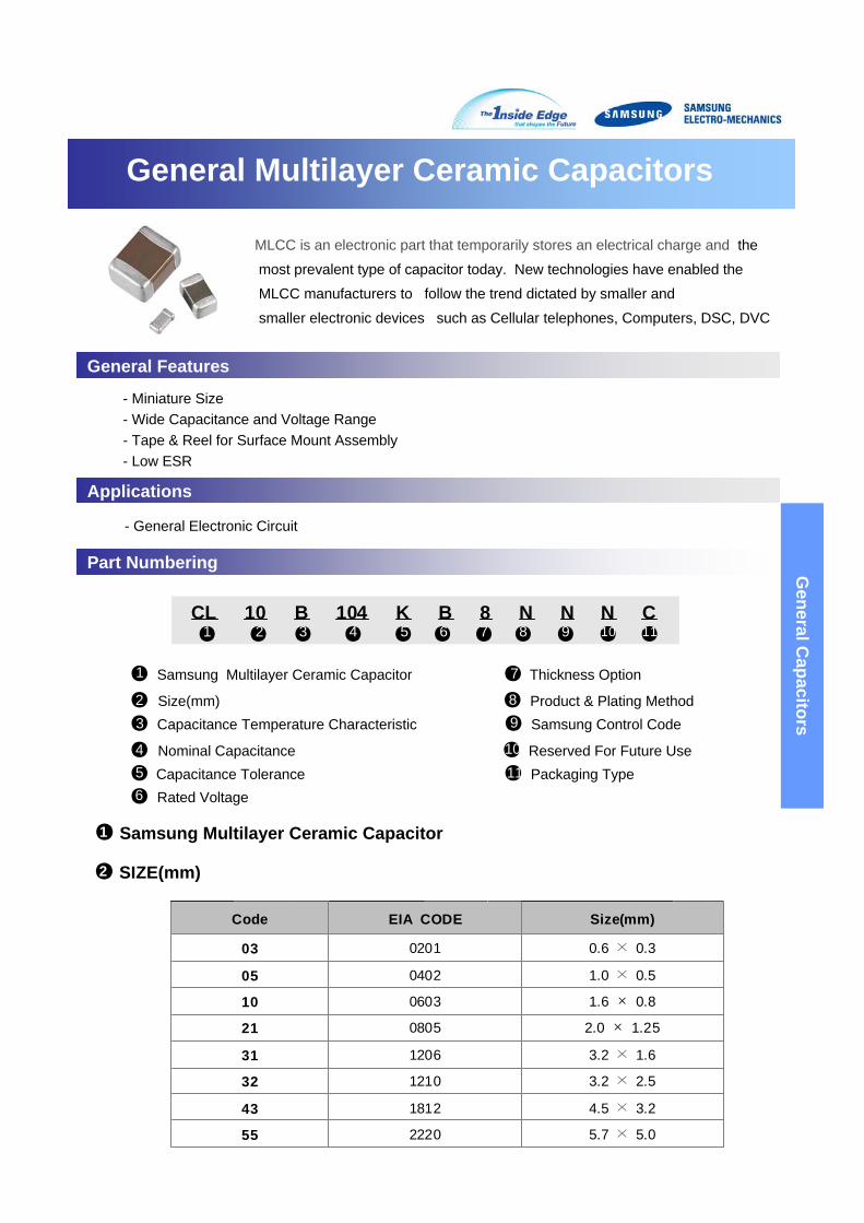
MLCC is an electronic part that temporarily stores an electrical charge and the
most prevalent type of capacitor today. New technologies have enabled the
MLCC manufacturers to follow the trend dictated by smaller and
smaller electronic devices such as Cellular telephones, Computers, DSC, DVC
Code Temperature CharacteristicsTemperature
Range
C
Class Ⅰ
COG C△ 0±30(ppm/℃)
-55 ~ +125℃
P P2H P△ -150±60
R R2H R△ -220±60
S S2H S△ -330±60
T T2H T△ -470±60
U U2J U△ -750±60
L S2L S△ +350 ~ -1000
A
Class Ⅱ
X5R X5R ±15% -55 ~ +85℃
B X7R X7R ±15% -55 ~ +125℃
X X6S X6S ±22% -55 ~ +105℃
F Y5V Y5V +22 ~ -82% -30 ~ +85℃
TemperatureCharacteristics Below 2.0pF 2.2 ~ 3.9pF Above 4.0pF Above 10pF
CΔ C0G C0G C0G C0G
PΔ - P2J P2H P2H
RΔ - R2J R2H R2H
SΔ - S2J S2H S2H
TΔ - T2J T2H T2H
UΔ - U2J U2J U2J
※ Temperature Characteristic
J : ±120PPM/℃, H : ±60PPM/℃, G : ±30PPM/℃
● CAPACITANCE TEMPERATURE CHARACTERISTIC3
Nominal capacitance is identified by 3 digits.The first and second digits identify the first and second significant figures of the capacitance.The third digit identifies the multiplier. 'R' identifies a decimal point.
Code Nominal Capacitance
1R5 1.5pF
103 10,000pF, 10nF, 0.01μF
104 100,000pF, 100nF, 0.1μF
● NOMINAL CAPACITANCE4
● Example
General C
apacitors
Code Tolerance Nominal Capacitance
A ±0.05pF
Less than 10pF(Including 10pF)
B ±0.1pF
C ±0.25pF
D ±0.5pF
F ±1pF
F ±1%
More than 10pF
G ±2%
J ±5%
K ±10%
M ±20%
Z +80, -20%
Code Rated Voltage Code Rated Voltage
R 4.0V D 200V
Q 6.3V E 250V
P 10V G 500V
O 16V H 630V
A 25V I 1,000V
L 35V J 2,000V
B 50V K 3,000V
C 100V
● CAPACITANCE TOLERANCE5
● RATED VOLTAGE6
General C
apacitors
● THICKNESS OPTION7
General C
apacitors
Code Electrode Termination Plating Type
A Pd Ag Sn_100%
N Ni Cu Sn_100%
G Cu Cu Sn_100%
Code Description of the code Code Description of the code
A Array (2-element) N Normal
B Array (4-element) P Automotive
C High - Q L LICC
● PRODUCT & PLATING METHOD8
● SAMSUNG CONTROL CODE9
Size Code Thickness(T) Size Code Thickness(T)
0201(0603) 3 0.30±0.03
1812(4532)
F 1.25±0.20
0402(1005) 5 0.50±0.05 H 1.6±0.20
0603(1608) 8 0.80±0.10 I 2.0±0.20
0805(2012)
A 0.65±0.10 J 2.5±0.20
C 0.85±0.10 L 3.2±0.30
F 1.25±0.10
2220(5750)
F 1.25±0.20
Q 1.25±0.15 H 1.6±0.20
Y 1.25±0.20 I 2.0±0.20
1206(3216)
C 0.85±0.15 J 2.5±0.20
F 1.25±0.15 L 3.2±0.30
H 1.6±0.20
1210(3225)
F 1.25±0.20
H 1.6±0.20
I 2.0±0.20
J 2.5±0.20
V 2.5±0.30
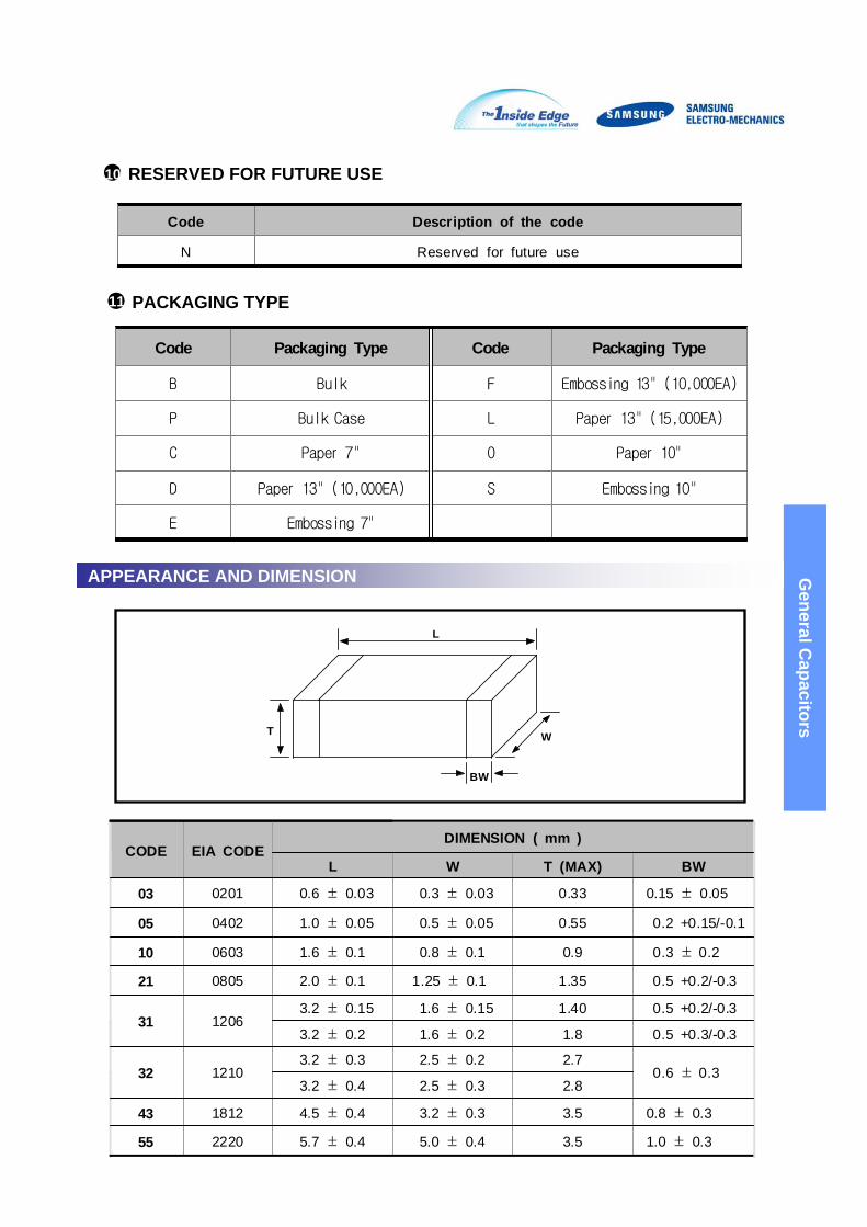
Code Description of the code
N Reserved for future use
Code Packaging Type Code Packaging Type
B Bulk F Embossing 13" (10,000EA)
P Bulk Case L Paper 13" (15,000EA)
C Paper 7" O Paper 10"
D Paper 13" (10,000EA) S Embossing 10"
E Embossing 7"
● RESERVED FOR FUTURE USE106
● PACKAGING TYPE11
General C
apacitors
APPEARANCE AND DIMENSION
L
BW
T W
CODE EIA CODEDIMENSION ( mm )
L W T (MAX) BW
03 0201 0.6 ± 0.03 0.3 ± 0.03 0.33 0.15 ± 0.05
05 0402 1.0 ± 0.05 0.5 ± 0.05 0.55 0.2 +0.15/-0.1
10 0603 1.6 ± 0.1 0.8 ± 0.1 0.9 0.3 ± 0.2
21 0805 2.0 ± 0.1 1.25 ± 0.1 1.35 0.5 +0.2/-0.3
31 12063.2 ± 0.15 1.6 ± 0.15 1.40 0.5 +0.2/-0.3
3.2 ± 0.2 1.6 ± 0.2 1.8 0.5 +0.3/-0.3
32 12103.2 ± 0.3 2.5 ± 0.2 2.7
0.6 ± 0.33.2 ± 0.4 2.5 ± 0.3 2.8
43 1812 4.5 ± 0.4 3.2 ± 0.3 3.5 0.8 ± 0.3
55 2220 5.7 ± 0.4 5.0 ± 0.4 3.5 1.0 ± 0.3
General C
apacitors
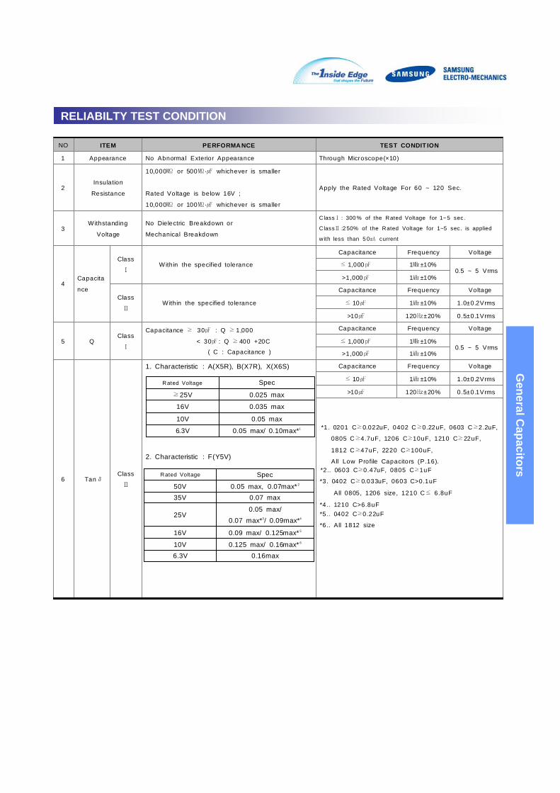
NO ITEM PERFORMA NCE TEST CONDIT ION
1 Appearance No Abnormal Exterior Appearance Through Microscope(×10)
2Insulation
Resistance
10,000㏁ or 500㏁ ·㎌ whichever is smaller
Rated Voltage is below 16V ;
10,000㏁ or 100㏁ ·㎌ whichever is smaller
Apply the Rated Voltage For 60 ~ 120 Sec.
3Withstanding
Voltage
No Dielectric Breakdown or
Mechanical Breakdown
ClassⅠ : 300 % of the Rated Voltage for 1~5 sec.
C lassⅡ :2 50% of the Rated Voltage for 1~5 sec. is applied
with less than 5 0㎃ current
4Capacita
nce
Class
ⅠWithin the specified tolerance
Capacitance Frequency Voltage
≤ 1,000㎊ 1㎒ ±10%0.5 ~ 5 Vrms
>1,000㎊ 1㎑ ±10%
Class
ⅡWithin the specified tolerance
Capacitance Frequency Voltage
≤ 10㎌ 1㎑ ±10% 1.0±0.2Vrms
>10㎌ 120㎐±20% 0.5±0.1Vrms
5 QClass
Ⅰ
Capacitance ≥ 30㎊ : Q ≥ 1,000
< 30㎊ : Q ≥ 400 +20C
( C : Capacitance )
Capacitance Frequency Voltage
≤ 1,000㎊ 1㎒ ±10%0.5 ~ 5 Vrms
>1,000㎊ 1㎑ ±10%
6 TanδClass
Ⅱ
1. Characteristic : A(X5R), B(X7R), X(X6S)
2. Characteristic : F(Y5V)
Capacitance Frequency Voltage
≤ 10㎌ 1㎑ ±10% 1.0±0.2Vrms
>10㎌ 120㎐±20% 0.5±0.1VrmsRated Voltage Spec
≥ 25V 0.025 max
16V 0.035 max
10V 0.05 max
6.3V 0.05 max/ 0.10max*1
Rated Voltage Spec
50V 0.05 max, 0.07max* 2
35V 0.07 max
25V0.05 max/
0.07 max*3/ 0.09max*4
16V 0.09 max/ 0.125max* 5
10V 0.125 max/ 0.16max* 6
6.3V 0.16max
*3. 0402 C≥0.033uF, 0603 C>0.1uF
All 0805, 1206 size, 1210 C≤ 6.8uF
*4.. 1210 C>6.8uF*5.. 0402 C≥0.22uF
*6.. All 1812 size
*2.. 0603 C≥0.47uF, 0805 C≥1uF
*1. 0201 C≥0.022uF, 0402 C≥0.22uF, 0603 C≥2.2uF,
0805 C≥4.7uF, 1206 C≥10uF, 1210 C≥22uF,
1812 C≥47uF, 2220 C≥100uF,
All Low Profile Capacitors (P.16).
RELIABILTY TEST CONDITION
General C
apacitors
NO ITEM PERFORMANCE TEST CONDITION
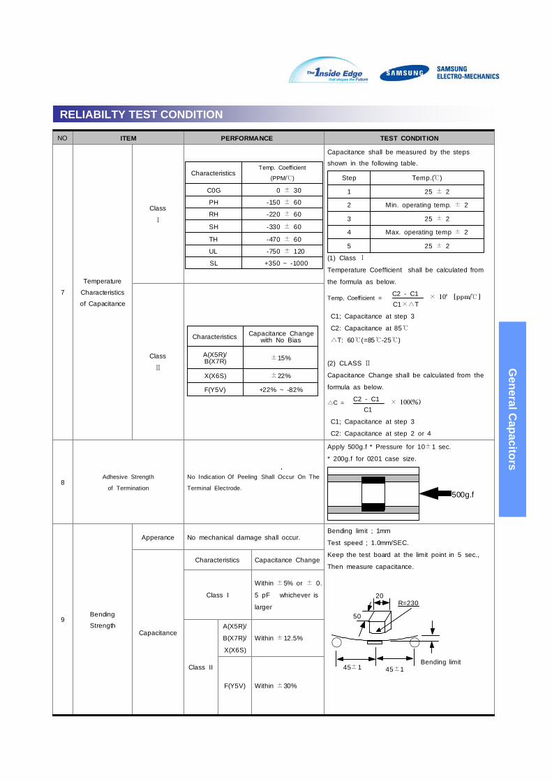
7
Temperature
Characteristics
of Capacitance
Class
Ⅰ
Capacitance shall be measured by the steps
shown in the following table.
(1) Class Ⅰ
Temperature Coefficient shall be calculated from
the formula as below.
C1×△T× 106 [ppm/℃]C2 - C1
Temp, Coefficient =
C1; Capacitance at step 3
C2: Capacitance at 85℃
△T: 60℃(=85℃-25℃)
(2) CLASS Ⅱ
Capacitance Change shall be calculated from the
formula as below.
× 100(%)C2 - C1C1
△C =
C1; Capacitance at step 3
C2: Capacitance at step 2 or 4
Class
Ⅱ
8Adhesive Strength
of Termination
No Indication Of Peeling Shall Occur On The
Terminal Electrode.
Apply 500g.f * Pressure for 10±1 sec.
* 200g.f for 0201 case size.
9Bending
Strength
Apperance No mechanical damage shall occur.Bending limit ; 1mm
Test speed ; 1.0mm/SEC.
Keep the test board at the limit point in 5 sec.,
Then measure capacitance.
Capacitance
Characteristics Capacitance Change
Class I
Within ±5% or ± 0.
5 pF whichever is
larger
Class II
A(X5R)/
B(X7R)/
X(X6S)
Within ±12.5%
F(Y5V) Within ±30%
Characteristics Capacitance Changewith No Bias
A(X5R)/B(X7R) ±15%
X(X6S) ±22%
F(Y5V) +22% ~ -82%
500g.f
CharacteristicsTemp. Coefficient
(PPM/℃)
C0G 0 ± 30
PH -150 ± 60
RH -220 ± 60
SH -330 ± 60
TH -470 ± 60
UL -750 ± 120
SL +350 ~ -1000
Step Temp.(℃)
1 25 ± 2
2 Min. operating temp. ± 2
3 25 ± 2
4 Max. operating temp ± 2
5 25 ± 2
○ ○
50
R=23020
45±1 45±1Bending limit
RELIABILTY TEST CONDITION
General C
apacitors
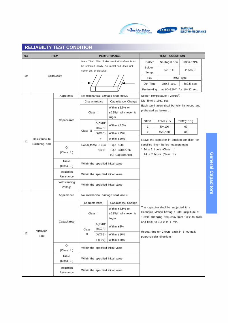
NO ITEM PERFORMANCE TEST CONDITION
10 Solderability
More Than 75% of the terminal surface is to
be soldered newly, So metal part does not
come out or dissolve
11Resistance to
Soldering heat
Apperance No mechanical damage shall occur. Solder Temperature : 270±5℃
Dip Time : 10±1 sec.
Each termination shall be fully immersed and
preheated as below :
Leave the capacitor in ambient condition for
specified time* before measurement
* 24 ± 2 hours (Class Ⅰ)
24 ± 2 hours (Class Ⅱ)
Capacitance
Characteristics Capacitance Change
Class Ⅰ
Within ±2.5% or
±0.25㎊ whichever is
larger
Class Ⅱ
A(X5R)/
B(X7R)Within ±7.5%
X(X6S) Within ±15%
F Within ±20%
Q
(Class Ⅰ)
Capacitance ≥ 30㎊ : Q≥ 1000
<30㎊ : Q≥ 400+20×C
(C: Capacitance)
Tanδ
(Class Ⅱ)Within the specified initial value
Insulation
ResistanceWithin the specified initial value
Withstanding
VoltageWithin the specified initial value
12Vibration
Test
Appearance No mechanical damage shall occur.
The capacitor shall be subjected to a
Harmonic Motion having a total amplitude of
1.5mm changing frequency from 10Hz to 55Hz
and back to 10Hz In 1 min.
Repeat this for 2hours each in 3 mutually
perpendicular directions
Capacitance
Characteristics Capacitance Change
Class Ⅰ
Within ±2.5% or
±0.25㎊ whichever is
larger
Class
Ⅱ
A(X5R)/
B(X7R)Within ±5%
X(X6S) Within ±10%
F(Y5V) Within ±20%
Q
(Class Ⅰ)Within the specified initial value
Tanδ
(Class Ⅱ)Within the specified initial value
Insulation
ResistanceWithin the specified initial value
STEP TEMP.(℃) TIME(SEC.)
1 80~100 60
2 150~180 60
Solder Sn-3Ag-0.5Cu 63Sn-37Pb
Solder
Temp.245±5℃ 235±5℃
Flux RMA Type
Dip Time 3±0.3 sec. 5±0.5 sec.
Pre-heating at 80~120℃ for 10~30 sec.
RELIABILTY TEST CONDITION
General C
apacitors
NO ITEM PERFORMANCE TEST CONDITION
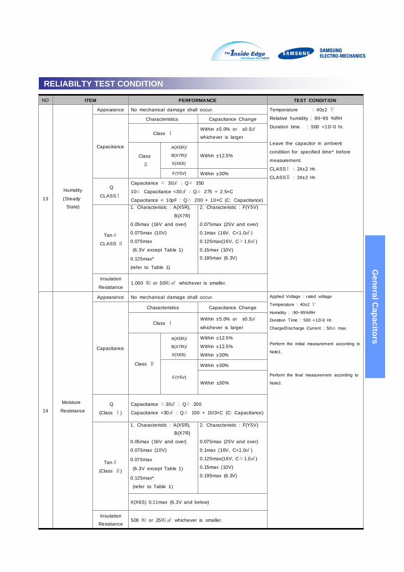
13
Humidity
(Steady
State)
Appearance No mechanical damage shall occur. Temperature : 40±2 ℃
Relative humidity : 90~95 %RH
Duration time : 500 +12/-0 hr.
Leave the capacitor in ambient
condition for specified time* before
measurement.
CLASSⅠ : 24±2 Hr.
CLASSⅡ : 24±2 Hr.
Capacitance
Characteristics Capacitance Change
Class ⅠWithin ±5.0% or ±0.5㎊
whichever is larger
Class
Ⅱ
A(X5R)/
B(X7R)/
X(X6S)
Within ±12.5%
F(Y5V) Within ±30%
Q
CLASSⅠ
Capacitance ≥ 30㎊ : Q≥ 350
10≤ Capacitance <30㎊ : Q≥ 275 + 2.5×C
Capacitance < 10pF : Q≥ 200 + 10×C (C: Capacitance)
Tanδ
CLASS Ⅱ
1. Characteristic : A(X5R),
B(X7R)
0.05max (16V and over)
0.075max (10V)
0.075max
(6.3V except Table 1)
0.125max*
(refer to Table 1)
2. Characteristic : F(Y5V)
0.075max (25V and over)
0.1max (16V, C<1.0㎌ )
0.125max(16V, C≥ 1.0㎌)
0.15max (10V)
0.195max (6.3V)
Insulation
Resistance1,000 ㏁ or 50㏁ ·㎌ whichever is smaller.
14
Moisture
Resistance
Appearance No mechanical damage shall occur. Applied Voltage : rated voltage
Temperature : 40±2 ℃
Humidity : :90~95%RH
Duration Time : 500 +12/-0 Hr.
Charge/Discharge Current : 50㎃ max.
Perform the initial measurement according to
Note1 .
Perform the final measurement according to
Note2.
Capacitance
Characteristics Capacitance Change
Class ⅠWithin ±5.0% or ±0.5㎊
whichever is larger
Class Ⅱ
A(X5R)/
B(X7R)/
X(X6S)
Within ±12.5%
Within ±12.5%
Within ±30%
F(Y5V)
Within ±30%
Within ±30%
Q
(Class Ⅰ)
Capacitance ≥ 30㎊ : Q≥ 200
Capacitance <30㎊ : Q≥ 100 + 10/3×C (C: Capacitance)
Tanδ
(Class Ⅱ)
1. Characteristic : A(X5R),
B(X7R)
0.05max (16V and over)
0.075max (10V)
0.075max
(6.3V except Table 1)
0.125max*
(refer to Table 1)
2. Characteristic : F(Y5V)
0.075max (25V and over)
0.1max (16V, C<1.0㎌ )
0.125max(16V, C≥ 1.0㎌)
0.15max (10V)
0.195max (6.3V)
X(X6S) 0.11max (6.3V and below)
Insulation
Resistance500 ㏁ or 25㏁·㎌ whichever is smaller.
RELIABILTY TEST CONDITION
General C
apacitors
NO ITEM PERFORMANCE TEST CONDITION
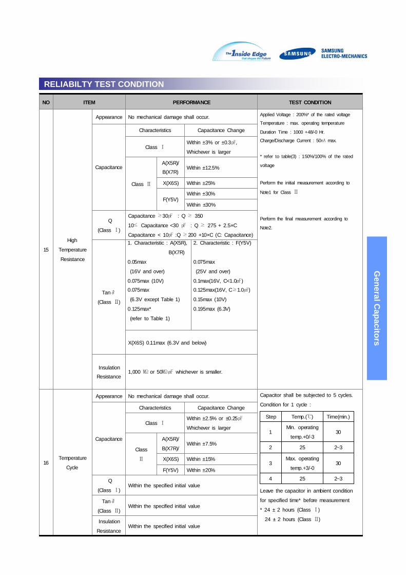
15
High
Temperature
Resistance
Appearance No mechanical damage shall occur. Applied Voltage : 200%* of the rated voltage
Temperature : max. operating temperature
Duration Time : 1000 +48/-0 Hr.
Charge/Discharge Current : 50㎃ max.
* refer to table(3) : 150%/100% of the rated
voltage
Perform the initial measurement according to
Note1 for Class Ⅱ
Perform the final measurement according to
Note2.
Capacitance
Characteristics Capacitance Change
Class ⅠWithin ±3% or ±0.3㎊,
Whichever is larger
Class Ⅱ
A(X5R)/
B(X7R)Within ±12.5%
X(X6S) Within ±25%
F(Y5V)Within ±30%
Within ±30%
Q
(Class Ⅰ)
Capacitance ≥30㎊ : Q ≥ 350
10≤ Capacitance <30 ㎊ : Q ≥ 275 + 2.5×C
Capacitance < 10㎊ :Q ≥ 200 +10×C (C: Capacitance)
Tanδ
(Class Ⅱ)
1. Characteristic : A(X5R),
B(X7R)
0.05max
(16V and over)
0.075max (10V)
0.075max
(6.3V except Table 1)
0.125max*
(refer to Table 1)
2. Characteristic : F(Y5V)
0.075max
(25V and over)
0.1max(16V, C<1.0㎌)
0.125max(16V, C≥1.0㎌)
0.15max (10V)
0.195max (6.3V)
X(X6S) 0.11max (6.3V and below)
Insulation
Resistance1,000 ㏁ or 50㏁·㎌ whichever is smaller.
16Temperature
Cycle
Appearance No mechanical damage shall occur. Capacitor shall be subjected to 5 cycles.
Condition for 1 cycle :
Step Temp.(℃) Time(min.)
1Min. operating
temp.+0/-330
2 25 2~3
3Max. operating
temp.+3/-030
4 25 2~3
Leave the capacitor in ambient condition
for specified time* before measurement
* 24 ± 2 hours (Class Ⅰ)
24 ± 2 hours (Class Ⅱ)
Capacitance
Characteristics Capacitance Change
Class ⅠWithin ±2.5% or ±0.25㎊
Whichever is larger
Class
Ⅱ
A(X5R)/
B(X7R)/Within ±7.5%
X(X6S) Within ±15%
F(Y5V) Within ±20%
Q
(Class Ⅰ)Within the specified initial value
Tanδ
(Class Ⅱ)Within the specified initial value
Insulation
ResistanceWithin the specified initial value
RELIABILTY TEST CONDITION
General C
apacitors
RELIABILTY TEST CONDITION
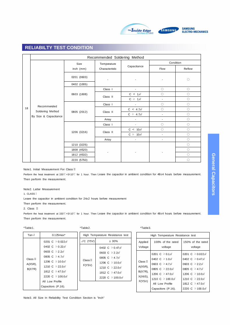
Note1. Initial Measurement For ClassⅡ
Perform the heat treatment at 150℃+0/-10℃ for 1 hour. Then Leave the capacitor in ambient condition for 48±4 hours before measurement.
Then perform the measurement.
Note2. Latter Measurement1. CLASSⅠ
Leave the capacitor in ambient condition for 24±2 hours before measurement
Then perform the measurement.
2. Class Ⅱ
Perform the heat treatment at 150℃+0/-10℃ for 1 hour. Then Leave the capacitor in ambient condition for 48±4 hours before measurement.
Then perform the measurement.
*Table1. *Table2. *Table3.
Note3. All Size In Reliability Test Condition Section is "inch"
18
Recommended Soldering Method
Recommended
Soldering Method
By Size & Capacitance
Size
inch (mm)
Temperature
CharacteristicCapacitance
Condition
Flow Reflow
0201 (0603)- - - ○
0402 (1005)
0603 (1608)
Class I - ○ ○
Class IIC < 1㎌ ○ ○
C ≥ 1㎌ - ○
0805 (2012)
Class I - ○ ○
Class IIC < 4.7㎌ ○ ○
C ≥ 4.7㎌ - ○
Array - - ○
1206 (3216)
Class I - ○ ○
Class IIC < 10㎌ ○ ○
C ≥ 10㎌ - ○
Array - - ○
1210 (3225)
- - -
○
1808 (4520) ○
1812 (4532) ○
2220 (5750) ○
High Temperature Resistance test
Applied
Voltage
100% of the rated
voltage
150% of the rated
voltage
ClassⅡ
A(X5R),
B(X7R),
X(X6S),
F(Y5V)
0201 C ≥ 0.1㎌
0402 C ≥ 1.0㎌
0603 C ≥ 4.7㎌
0805 C ≥ 22.0㎌
1206 C ≥ 47.0㎌
1210 C ≥ 100.0㎌
All Low Profile
Capacitors (P.16).
0201 C ≥ 0.022㎌
0402 C ≥ 0.47㎌
0603 C ≥ 2.2㎌
0805 C ≥ 4.7㎌
1206 C ≥ 10.0㎌
1210 C ≥ 22.0㎌
1812 C ≥ 47.0㎌
2220 C ≥ 100.0㎌
High Temperature Resistance test
ΔC (Y5V) ± 30%
ClassⅡ
F(Y5V)
0402 C ≥ 0.47㎌
0603 C ≥ 2.2㎌
0805 C ≥ 4.7㎌
1206 C ≥ 10.0㎌
1210 C ≥ 22.0㎌
1812 C ≥ 47.0㎌
2220 C ≥ 100.0㎌
Tanδ 0.125max*
ClassⅡ
A(X5R),
B(X7R)
0201 C ≥ 0.022㎌
0402 C ≥ 0.22㎌
0603 C ≥ 2.2㎌
0805 C ≥ 4.7㎌
1206 C ≥ 10.0㎌
1210 C ≥ 22.0㎌
1812 C ≥ 47.0㎌
2220 C ≥ 100.0㎌
All Low Profile
Capacitors (P.16).
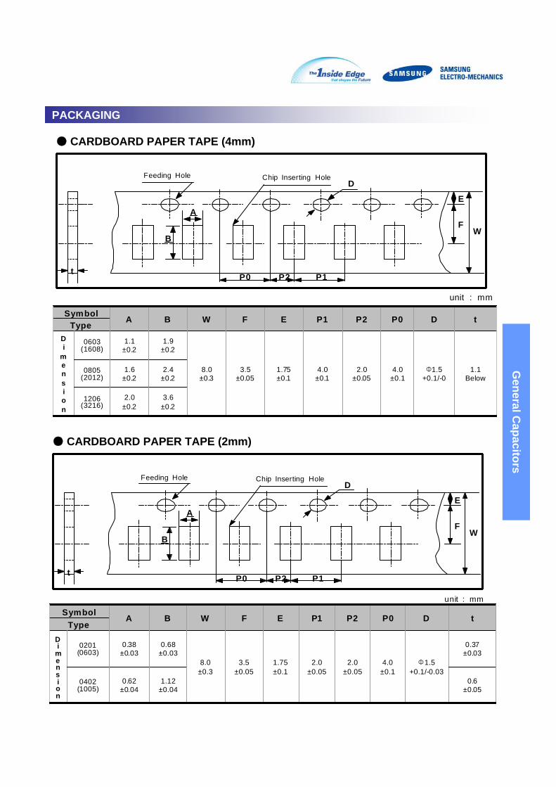
PACKAGING
General C
apacitors
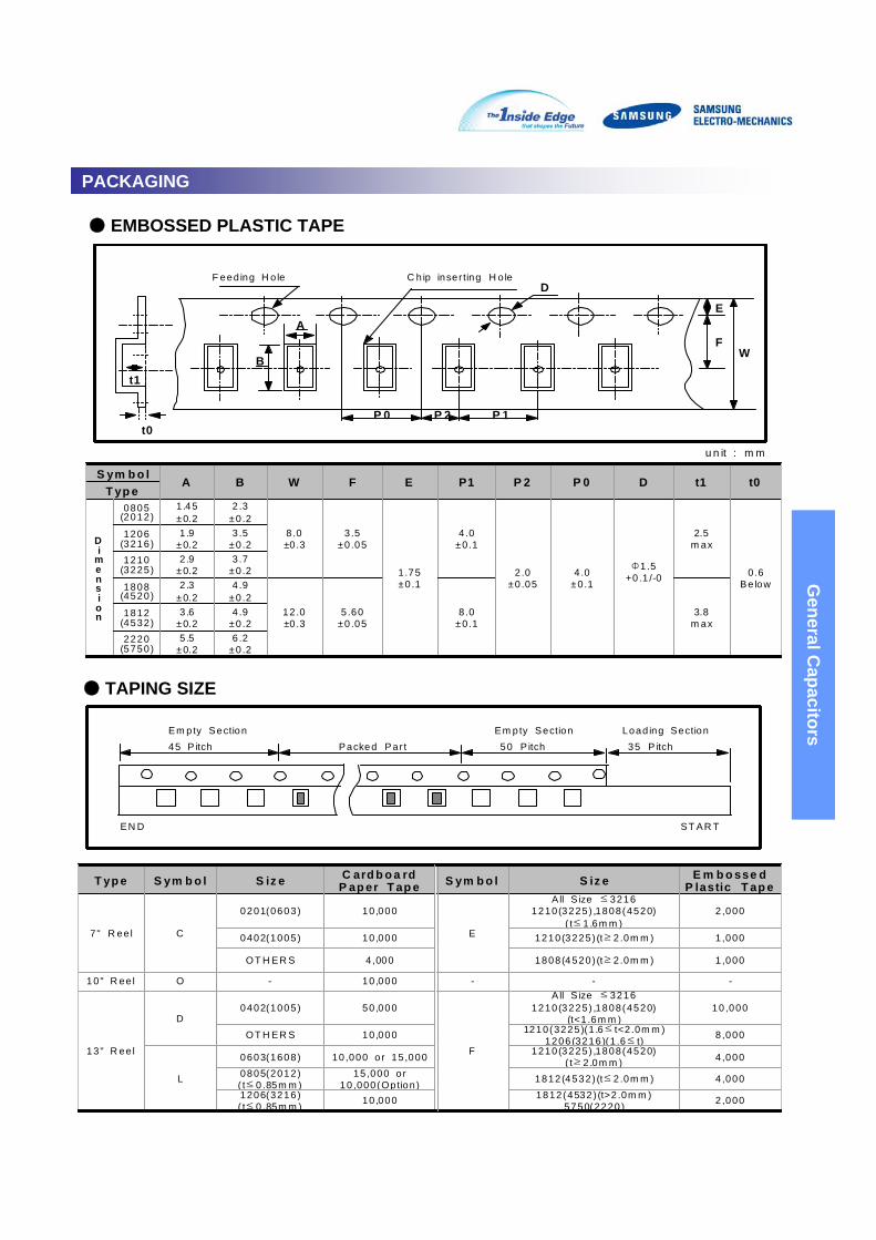
Symbol A B W F E P1 P2 P0 D tType
Di
mension
0603(1608)
1.1±0.2
1.9±0.2
8.0±0.3
3.5±0.05
1.75±0.1
4.0±0.1
2.0±0.05
4.0±0.1
Φ1.5+0.1/-0
1.1Below
0805(2012)
1.6±0.2
2.4±0.2
1206(3216)
2.0±0.2
3.6±0.2
unit : mm
Symbol A B W F E P1 P2 P0 D tType
Di
mension
0201(0603)
0.38±0.03
0.68±0.03
8.0±0.3
3.5±0.05
1.75±0.1
2.0±0.05
2.0±0.05
4.0±0.1
Φ1.5+0.1/-0.03
0.37±0.03
0402(1005)
0.62±0.04
1.12±0.04
0.6±0.05
unit : mm
A
B
Feeding HoleD
P0 P1P2
WF
E
t
A
B
Feeding Hole Chip Inserting HoleD
P0 P1P2
WF
E
t
Chip Inserting Hole
● CARDBOARD PAPER TAPE (4mm)
● CARDBOARD PAPER TAPE (2mm)
PACKAGING
General C
apacitors
S ym b o l A B W F E P1 P 2 P 0 D t1 t0T yp e
Di
mension
0805(2012)
1 .45±0.2
2 .3±0 .2
8 .0±0 .3
3 .5±0 .05
1 .75±0 .1
4 .0±0 .1
2 .0±0 .05
4 .0±0 .1
Φ1.5+0 .1 /-0
2.5m ax
0.6Be low
1206(3216)
1 .9±0.2
3 .5±0 .2
1210(3225)
2 .9±0.2
3 .7±0 .2
1808(4520)
2 .3±0.2
4 .9±0 .2
12 .0±0 .3
5 .60±0 .05
8 .0±0 .1
3.8m ax
1812(4532)
3 .6±0.2
4 .9±0 .2
2220(5750)
5 .5±0.2
6 .2±0 .2
u n it : m m
A
B
F eed ing H o le C h ip inser ting H o leD
P 0 P 1P 2
WF
E
t1
t0
Em pty Section45 P itch Packed Par t
Em pty Section50 P itch
Load ing Section35 P itch
ST AR TEN D
T yp e S ym b o l S iz e C ard b o a rdP ap er T ap e S ym b o l S iz e E m b o sse d
P lastic T ap e
7" R ee l C
0201(0603) 10 ,000
E
A ll S ize ≤ 32161210(3225) ,1808(4520)
( t≤ 1.6m m )2 ,000
0402(1005) 10 ,000 1210(3225) (t≥ 2.0m m ) 1 ,000
OT H ER S 4,000 1808(4520) (t≥ 2.0m m ) 1 ,000
10" R ee l O - 10 ,000 - - -
13" R ee l
D0402(1005) 50 ,000
F
A ll S ize ≤ 32161210(3225) ,1808(4520)
(t<1 .6m m )10 ,000
OT H ER S 10,000 1210(3225)(1 .6≤ t<2 .0m m )1206 (3216)(1 .6≤ t) 8 ,000
L
0603(1608) 10 ,000 or 15 ,000 1210(3225) ,1808(4520)( t≥ 2.0m m ) 4 ,000
0805(2012)( t≤ 0.85m m )
15,000 or10 ,000(Option) 1812(4532) (t≤ 2.0m m ) 4 ,000
1206(3216)( t≤ 0.85m m ) 10,000 1812(4532 )(t>2 .0m m )
5750(2220 ) 2 ,000
● EMBOSSED PLASTIC TAPE
● TAPING SIZE
General C
apacitors
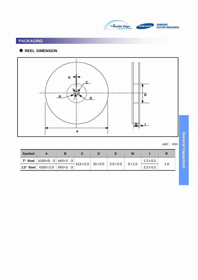
● REEL DIMENSION
EC
DR
A
W
B
t
unit : mm
Symbol A B C D E W t R
7" Reel φ180+0/ -3 φ60+1/ -3φ13±0.3 25±0.5 2.0±0.5 9±1.5
1.2±0.21.0
13" Reel φ330±2.0 φ80+1/ -3 2.2±0.2
PACKAGING
General C
apacitors
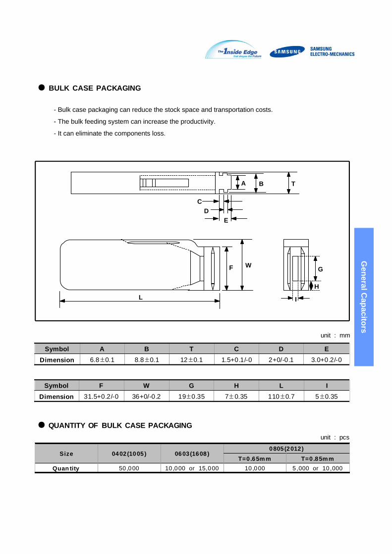
● BULK CASE PACKAGING
A B T
CD
E
F W
L
G
H
I
unit : mm
Symbol A B T C D EDimension 6.8±0.1 8.8±0.1 12±0.1 1.5+0.1/-0 2+0/-0.1 3.0+0.2/-0
Symbol F W G H L IDimension 31.5+0.2/-0 36+0/-0.2 19±0.35 7±0.35 110±0.7 5±0.35
● QUANTITY OF BULK CASE PACKAGING
Size 0402(1005) 0603(1608)0805(2012)
T=0.65mm T=0.85mmQuan tity 50 ,000 10,000 or 15,000 10 ,000 5 ,000 or 10 ,000
unit : pcs
- Bulk case packaging can reduce the stock space and transportation costs.
- The bulk feeding system can increase the productivity.
- It can eliminate the components loss.
APPLICATION MANUAL
General C
apacitors
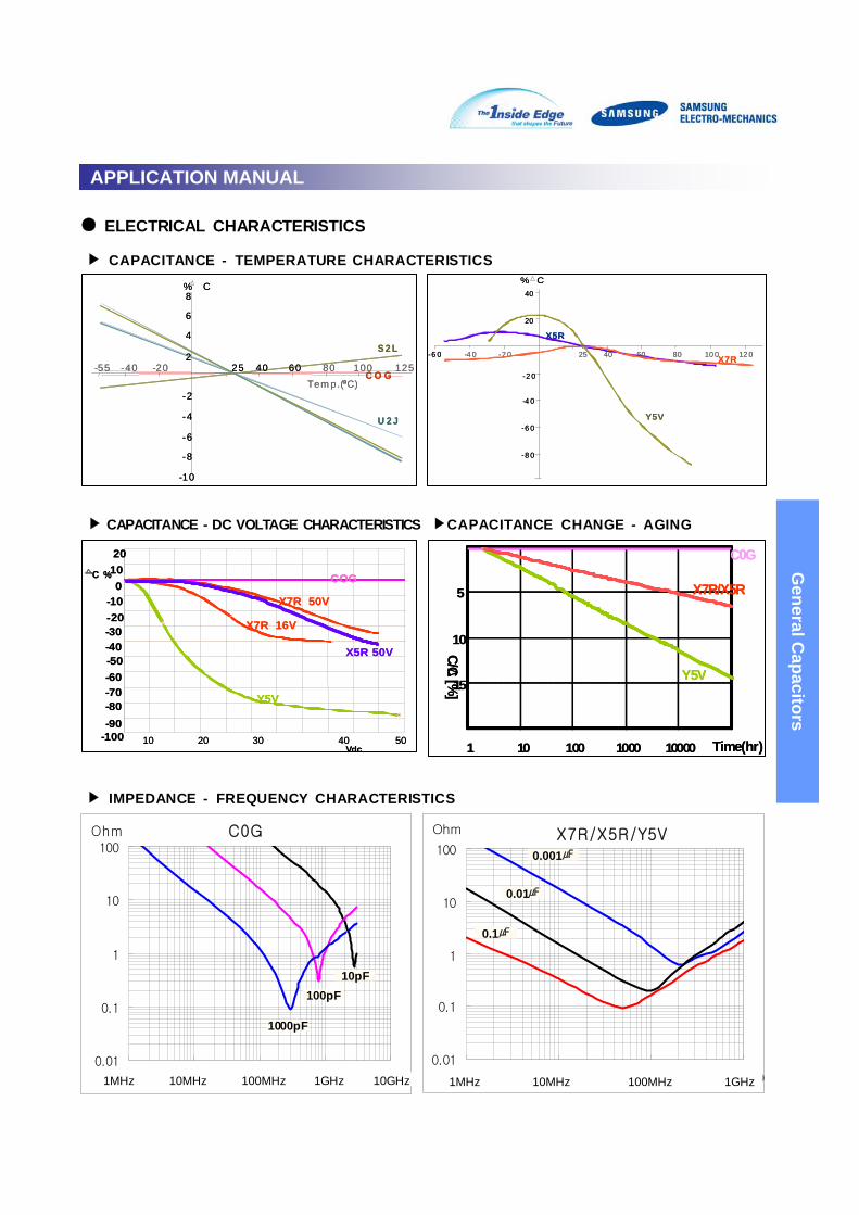
● ELECTRICAL CHARACTERISTICS
▶CAPACITANCE CHANGE - AGING
▶ IMPEDANCE - FREQUENCY CHARACTERISTICS
▶ CAPACITANCE - DC VOLTAGE CHARACTERISTICS
C0G
0.01
0.1
1
10
100
1.E+06 1.E+07 1.E+08 1.E+09 1.E+10
Ohm
1MHz 10MHz 100MHz 1GHz 10GHz
1000pF
100pF10pF
X7R/X5R/Y5V
0.01
0.1
1
10
100
1.E+06 1.E+07 1.E+08 1.E+09
Ohm
0.1㎌
0.01㎌
0.001㎌
1MHz 10MHz 100MHz 1GHz
▶ CAPACITANCE - TEMPERATURE CHARACTERISTICS
40
20
-2 0
-4 0
-6 0
-8 0
-2 0-4 0-6 0 25 40 60 80 10 0 12 0X7R
X5R
Y5V
% C40
20
-2 0
-4 0
-6 0
-8 0
-2 0-4 0-6 0 25 40 60 80 10 0 12 0X7R
X5R
Y5V
% C
20
10 20 30 40 50
X7R 50V
X7R 16V
Y5V
C %
Vdc
COG
X5R 50V
100
-10-20-30-40-50-60-70-80-90
-100
20
10 20 30 40 50
X7R 50V
X7R 16V
Y5V
C %
Vdc
COG
X5R 50V
100
-10-20-30-40-50-60-70-80-90
-1001 10 100 1000 10000 Time(hr)
ΔC/C
[%]
Y5V
C0G
X7R/X5R5
10
15
1 10 100 1000 10000 Time(hr)
ΔC/C
[%]
Y5V
C0G
X7R/X5R5
10
15
8
6
4
2
-4
-6
-8
-10
-2
-55 -40 -20 25 40 60 80 100 125
S 2 L
U 2 J
C O G
% C
Tem p.(oC)o
8
6
4
2
-4
-6
-8
-10
-2
-55 -40 -20 25 40 60 80 100 125
S 2 L
U 2 J
C O G
% C
Tem p.(oC)o
W b
aSolderLand
So lder R esist
2/3 W < b < W
TSolder R esist
2/3 T < a < T
General C
apacitors
● STORAGE CONDITION
▶ Storage Environment
The electrical characteristics of MLCCs were degraded by the environment of high temperature or
humidity. Therefore, the MLCCs shall be stored in the ambient temperature and the relative humidity
of less than 40℃ and 70%, respectively.
Guaranteed storage period is within 6 months from the outgoing date of delivery.
▶ Corrosive Gases
Since the solderability of the end termination in MLCC was degraded by a chemical atmosphere
such as chlorine, acid or sulfide gases, MLCCs must be avoid from these gases.
▶ Temperature Fluctuations
Since dew condensation may occur by the differences in temperature when the MLCCs are taken
out of storage, it is important to maintain the temperature-controlled environment.
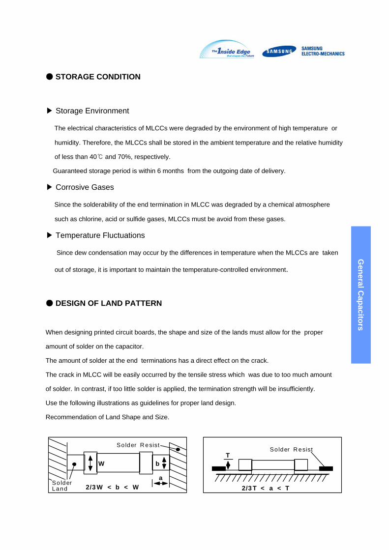
● DESIGN OF LAND PATTERN
When designing printed circuit boards, the shape and size of the lands must allow for the proper
amount of solder on the capacitor.
The amount of solder at the end terminations has a direct effect on the crack.
The crack in MLCC will be easily occurred by the tensile stress which was due to too much amount
of solder. In contrast, if too little solder is applied, the termination strength will be insufficiently.
Use the following illustrations as guidelines for proper land design.
Recommendation of Land Shape and Size.
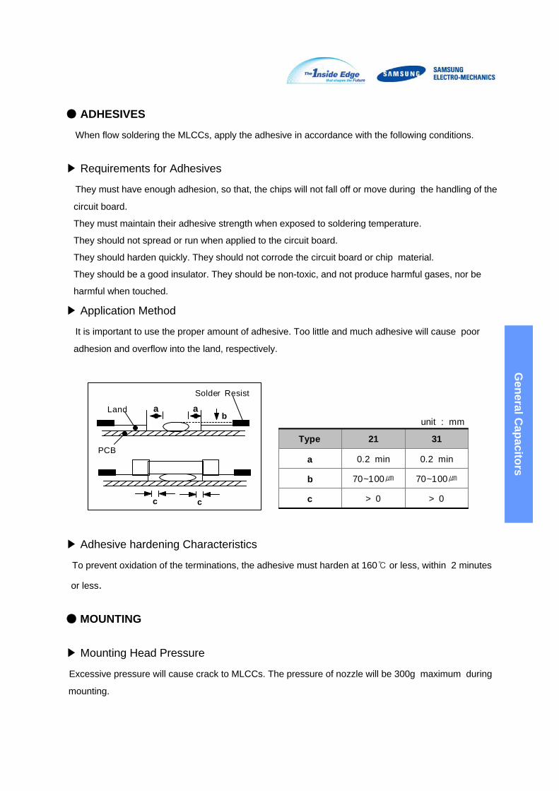
● ADHESIVES
When flow soldering the MLCCs, apply the adhesive in accordance with the following conditions.
▶ Requirements for Adhesives
They must have enough adhesion, so that, the chips will not fall off or move during the handling of the
circuit board.
They must maintain their adhesive strength when exposed to soldering temperature.
They should not spread or run when applied to the circuit board.
They should harden quickly. They should not corrode the circuit board or chip material.
They should be a good insulator. They should be non-toxic, and not produce harmful gases, nor be
harmful when touched.
▶ Application Method
It is important to use the proper amount of adhesive. Too little and much adhesive will cause poor
adhesion and overflow into the land, respectively.
▶ Adhesive hardening Characteristics
To prevent oxidation of the terminations, the adhesive must harden at 160℃ or less, within 2 minutes
or less.
● MOUNTING
▶ Mounting Head Pressure
Excessive pressure will cause crack to MLCCs. The pressure of nozzle will be 300g maximum during
mounting.
Solder Resist
Land
PCB
a ab
c c
Type 21 31
a 0.2 min 0.2 min
b 70~100㎛ 70~100㎛
c > 0 > 0
unit : mm
General C
apacitors
Too muchSolde r
N ot eno ug hSolde r
C racks tend to occur dueto larg e stress
W eak hold ing force maycause bad conne ctions or
detach ing of the capacitor
Goo d
support pin
force
nozzle
General C
apacitors
▶ Bending Stress
When double-sided circuit boards are used, MLCCs first are mounted and soldered onto one side of the
board. When the MLCCs are mounted onto the other side,
it is important to support the board as shown in the illustration. If the circuit board is not supported,
the crack occur to the ready-installed MLCCs by the bending stress.
▶ Manual Soldering
Manual soldering can pose a great risk of creating thermal cracks in chip capacitors.
The hot soldering iron tip comes into direct contact with the end terminations, and operator's
carelessness may cause the tip of the soldering iron to come into direct contact with the ceramic
body of the capacitor.
Therefore the soldering iron must be handled carefully, and close attention must be paid
to the selection of the soldering iron tip and to temperature control of the tip.
▶ Amount of Solder
Pre-heatingGradual cooling
in the airSoldering
Temp.(℃)
260+0/-5℃
10sec.max.
Time(sec)
Reflow
200℃
150℃
General C
apacitors
▶ Cooling
Natural cooling using air is recommended. If the chips are dipped into solvent for cleaning, the temperature difference(△T) must be less than 100℃
▶ Cleaning
If rosin flux is used, cleaning usually is unnecessary. When strongly activated flux is used, chlorine in the flux may dissolve into some types of cleaning fluids, thereby affecting the chip capacitors. This means that the cleaning fluid must be carefully selected, and should always be new.
▶ Notes for Separating Multiple, Shared PC Boards.
A multi-PC board is separated into many individual circuit boards after soldering has been completed. If the board is bent or distorted at the time of separation, cracks may occur in the chip capacitors. Carefully choose a separation method that minimizes the bending often circuit board.
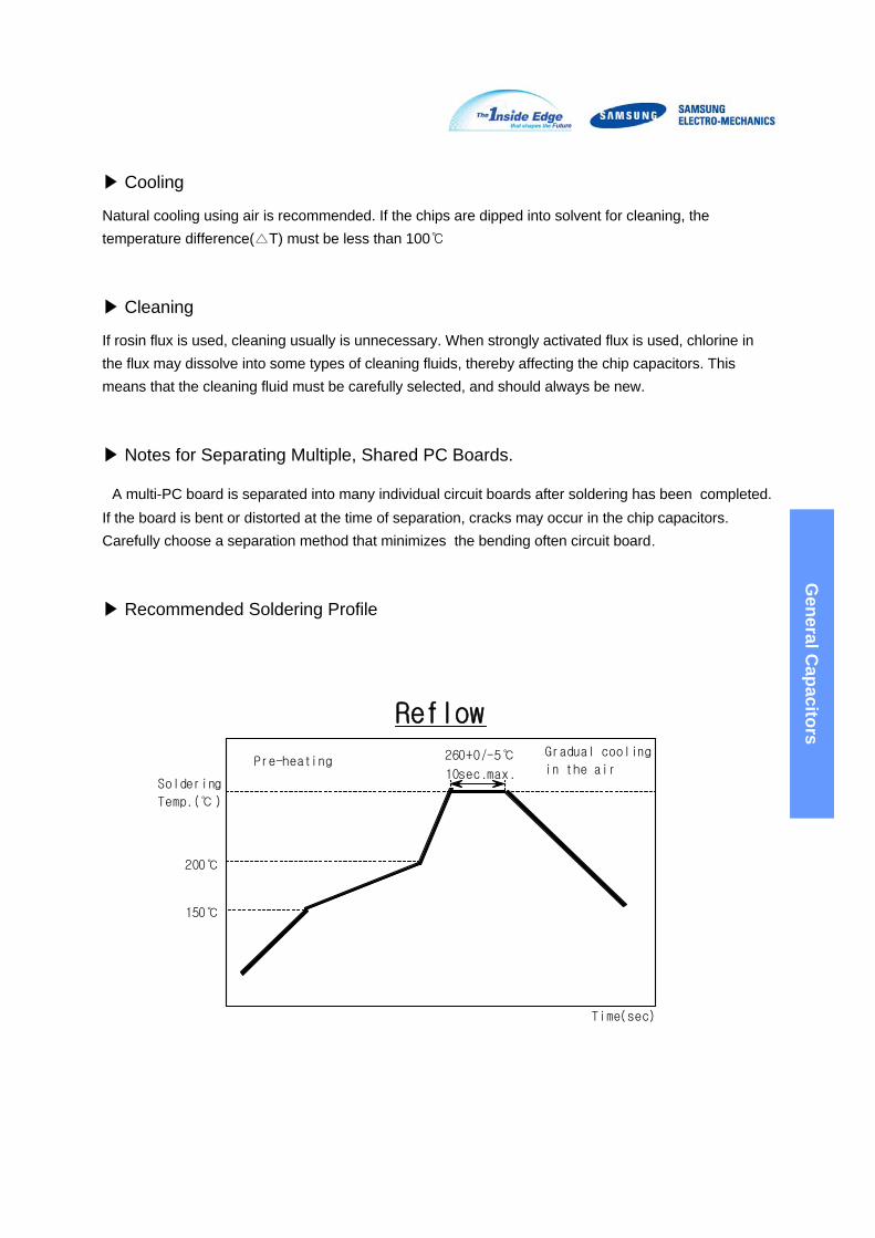
▶ Recommended Soldering Profile
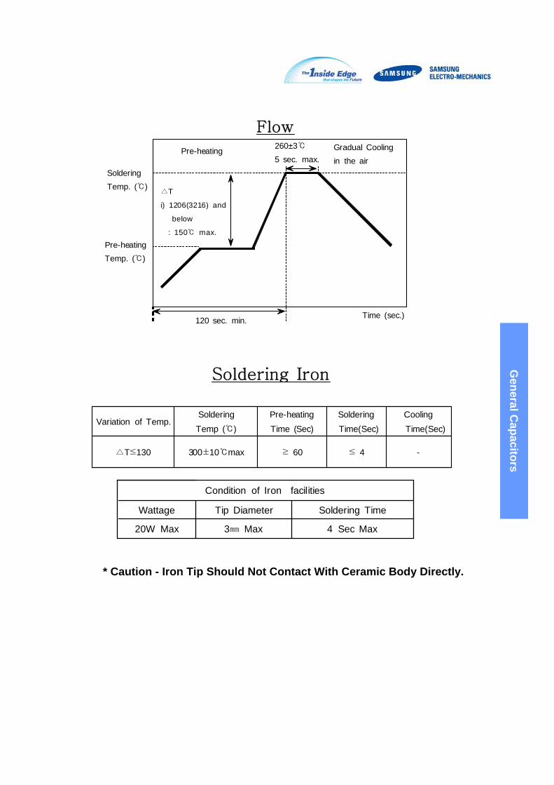
△T
i) 1206(3216) and
below
: 150℃ max.
Pre-heating Gradual Coolingin the air
SolderingTemp. (℃)
Pre-heatingTemp. (℃)
120 sec. min.
260±3℃
5 sec. max.
Time (sec.)
Flow
Soldering Iron
Variation of Temp.SolderingTemp (℃)
Pre-heatingTime (Sec)
SolderingTime(Sec)
CoolingTime(Sec)
△T≤130 300±10℃max ≥ 60 ≤ 4 -
Condition of Iron facilities
Wattage Tip Diameter Soldering Time
20W Max 3㎜ Max 4 Sec Max
* Caution - Iron Tip Should Not Contact With Ceramic Body Directly.
General C
apacitors