general-purpose electronic volume with built-in advanced...
TRANSCRIPT

Datasheet
Product structure:Silicon monolithic integrated circuit This product is not designed protection against radioactive rays
1/44
TSZ02201-0C2C0E100010-1-2
© 2013 ROHM Co., Ltd. All rights reserved. 4.OCT.2013 Rev.002
www.rohm.com
TSZ22111・14・001
Sound Processors for Car Audios
General-Purpose Electronic Volume with Built-in Advanced Switch BD37034FV-M
General Description
BD37034FV-M is sound processors for car audio. The functions are stereo 5 input selector, volume, 3-band equalizer, loudness, 6ch fader, mixing, HPF for front and rear, LPF for subwoofer, anti-aliasing-filter, Hi-Voltage output, output level detector. Moreover, “Advanced switch circuit”, that is ROHM original technology, can reduce various switching noise (ex. No-signal, low frequency likes 20Hz & large signal inputs). “Advanced switch” makes control of microcomputer easier, and can construct high quality car audio system.
Features Reduce switching noise of volume, mute, fader
volume, mixing volume, bass, middle, treble, loudness by using advanced switch circuit [Possible to control all steps].
Built-in input selector (single 3 / diff 2). Decrease the number of external components by
built-in 3-band equalizer filter, LPF for subwoofer, loudness filter. And, possible to control Q, Gv, fo of 3-band equalizer and fc of LPF, Gv, fo of loudness by I2C BUS control freely.
Built-in mixing volume, Hi-Voltage output. Built-in anti-aliasing-filter, anti-GSM-noise-filter. Package is SSOP-B28. Putting input-terminals
together and output-terminals together can make PCB layout easier and can makes area of PCB smaller.
It is possible to control by 3.3V / 5V for I2C BUS. AEC-Q100 Qualified.
Applications It is the optimal for the car audio. Besides, it is
possible to use for the audio equipment of mini Compo, micro Compo, TV etc with all kinds.
Key Specifications Total harmonic distortion: 0.004%(Typ.) Maximum input voltage: 2.1Vrms(Typ.) Cross-talk between selectors: 100dB(Typ.) Ripple rejection -65dB(Typ.) Output noise voltage: 6µVrms(Typ.) Residual output noise voltage: 4µVrms(Typ.) Operating Range of Temperature: -40 to +85
package(s) W(Typ.) x D(Typ.) x H(Max.)
SSOP-B28 10.00mm x 7.60mm x 1.35mm
SSOP-B28
Typical Application Circuit
Figure 1. Application Circuit Diagram

2/44
DatasheetBD37034FV-M
TSZ02201-0C2C0E100010-1-2
© 2013 ROHM Co., Ltd. All rights reserved. 4.OCT.2013 Rev.002
www.rohm.com
TSZ22111・15・001
Pin Configuration Pin Descriptions
Terminal Number
Terminal Name Description
Terminal Number
Terminal Name Description
1 A1 A input terminal of 1ch 15 MUTE External compulsory mute terminal
2 A2 A input terminal of 2ch 16 LRST/OLDC ・Level meter reset terminal ・Filter output terminal of output level
detector
3 B1 B input terminal of 1ch 17 LOUT/OLD ・Output terminal for Level meter ・Output terminal of output level
detector
4 B2 B input terminal of 2ch 18 OUTS2 SW output terminal of 2ch
5 C1 C input terminal of 1ch 19 OUTS1 SW output terminal of 1ch
6 C2 C input terminal of 2ch 20 OUTR2 Rear output terminal of 2ch
7 DP1 D positive input terminal of 1ch 21 OUTR1 Rear output terminal of 1ch
8 DN D negative input terminal 22 OUTF2 Front output terminal of 2ch
9 DP2 D positive input terminal of 2ch 23 OUTF1 Front output terminal of 1ch
10 EP1 E positive input terminal of 1ch 24 VCCL VCCL terminal for power supply
11 EN1 E negative input terminal of 1ch 25 SCL I2C Communication clock terminal
12 MIN/EN2 ・Mixing input terminal ・E negative input terminal of 2ch 26 SDA I2C Communication data terminal
13 EP2 E positive input terminal of 2ch 27 GND GND terminal
14 VCCH VCCH terminal for power supply 28 VREF VREF terminal
Figure 2. Pin configuration
A1 1
SSOP-B28 (TOP VIEW)
A2 2
B1 3
B2 4
C1 5
C2 6
DP1 7
DN 8
DP2 9
EP1 10
EN1 11
MIN/EN2 12
EP2 13
VCCH 14
19 OUTS1
18 OUTS2
17 LOUT/OLD
16 LRST/OLDC
15 MUTE
24 VCCL
23 OUTF1
22 OUTF2
21 OUTR1
20 OUTR2
28 VREF
27 GND
26 SDA
25 SCL

3/44
DatasheetBD37034FV-M
TSZ02201-0C2C0E100010-1-2
© 2013 ROHM Co., Ltd. All rights reserved. 4.OCT.2013 Rev.002
www.rohm.com
TSZ22111・15・001
Block Diagram
Figure 3. Block Diagram
Absolute Maximum Ratings Parameter Symbol Limits Unit
Power supply Voltage VCCL※1 10.0 V
VCCH※1 13.5 V
Input Voltage Vin※1 VCCL+0.3 to GND-0.3 Only SCL,SDA 7 to GND-0.3 V
Power Dissipation Pd 1.06 ※2 W
Storage Temperature Tastg -55 to +150 ※Maximum voltage which can be impressed referencing GND. Operation using batteries which is used in automobiles directly cannot be guaranteed. ※2 This value decreases 8.5mW/ for Ta=25 or more. ROHM standard board shall be mounted Thermal resistance θja = 117.6(/W) ROHM Standard board Size:70×70×1.6() Material:A FR4 grass epoxy board(3% or less of copper foil area)
Operating Range
Parameter Symbol Limits Unit
Power supply voltage VCCL 7.0 to 9.5 V
VCCH VCCL to 13.0 V
Temperature Topr -40 to +85

4/44
DatasheetBD37034FV-M
TSZ02201-0C2C0E100010-1-2
© 2013 ROHM Co., Ltd. All rights reserved. 4.OCT.2013 Rev.002
www.rohm.com
TSZ22111・15・001
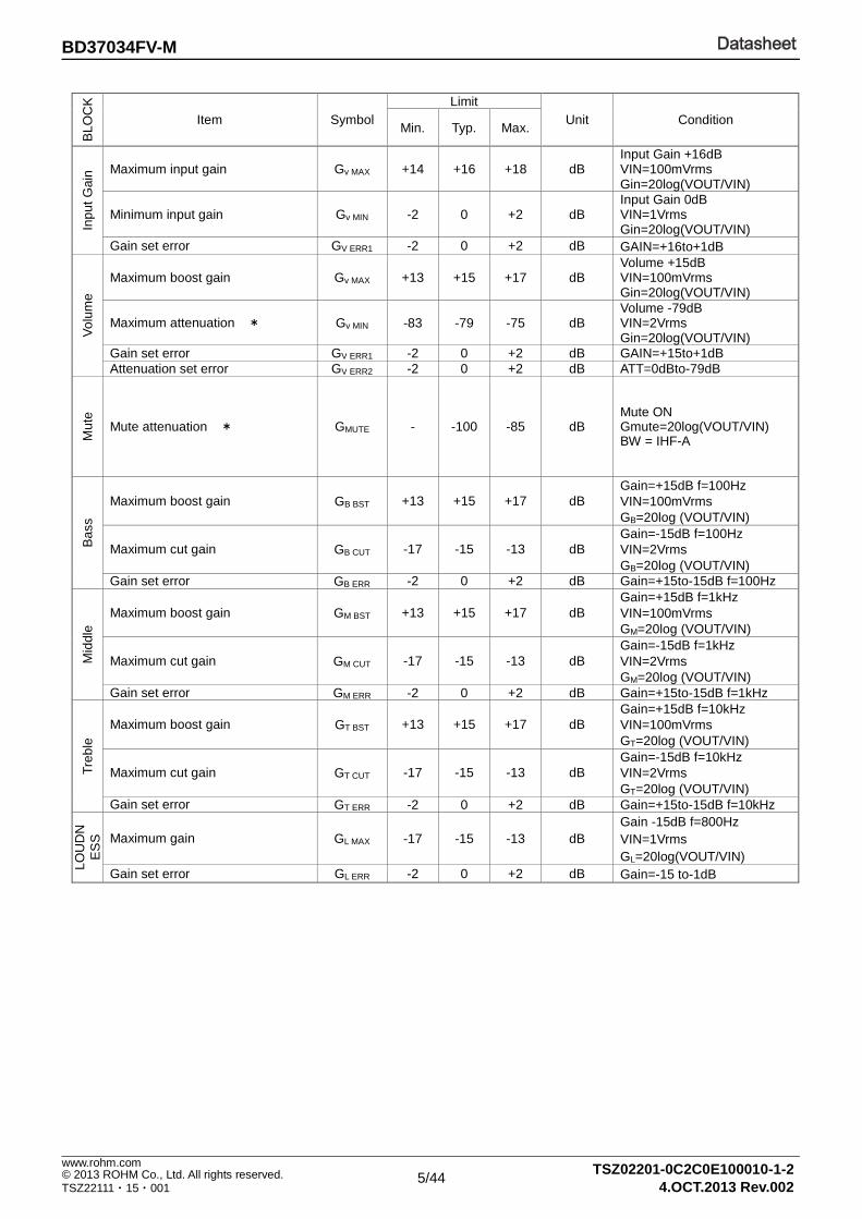
Electrical Characteristic Unless specified particularly Ta=25, VCCL=VCCH=8.5V, f=1kHz, Vin=1Vrms, Rg=600Ω, RL=10kΩ, A input Input Gain, Volume, Tone control, Loudness, Fader=0dB, LPF, HPF=OFF, Mix OFF, anti-aliasing-filter OFF
BLO
CK
Item Symbol Limit
Unit Condition Min. Typ. Max.
GE
NE
RA
L
Current upon no signal IQ - 36 49 mA No signal Voltage gain GV -1.5 0 +1.5 dB Gv=20log(VOUT/VIN) Channel balance CB -1.5 0 +1.5 dB CB = GV1-GV2
Total harmonic distortion 1 *
THD+N1 - 0.004 0.05 % VOUT=1Vrms BW=400-30KHz VCCH=8.5V(Hi-Voltage OFF)
Total harmonic distortion 2 * THD+N2 - 0.002 0.05 % VIN=1Vrms BW=400-30KHz VCCH=12V(Hi-Voltage ON)
Output noise voltage 1 * VNO1 - 6 12 µVrms Rg = 0Ω BW = IHF-A VCCH=8.5V(Hi-Voltage OFF)
Front/Rear Output noise voltage 2 Front/Rear * VNO2 - 16 32 µVrms
Rg = 0Ω BW = IHF-A VCCH=12V(Hi-Voltage ON)
Subwoofer Output noise voltage 3 Subwoofer * VNO3 - 22 44 µVrms
Rg = 0Ω BW = IHF-A VCCH=12V(Hi-Voltage ON)
Residual output noise voltage 1* VNOR1 - 4 10 µVrms Fader = -∞dB Rg = 0Ω, BW = IHF-A VCCH=8.5V(Hi-Voltage OFF)
Front/Rear Residual output noise voltage 2 Front/Rear* VNOR2 - 11 22 µVrms
Fader = -∞dB Rg = 0Ω, BW = IHF-A VCCH=12V(Hi-Voltage ON)
Subwoofer Residual output noise voltage 3 Subwoofer* VNOR3 - 16 32 µVrms
Fader = -∞dB Rg = 0Ω,BW = IHF-A VCCH=12V(Hi-Voltage ON)
Cross-talk between channels * CTC - -100 -85 dB Rg = 0Ω CTC=20log(VOUT/VIN) BW = IHF-A
Ripple rejection RR - -65 -40 dB f=1kHz, VRR=100mVrms RR=20log(VCC IN/VOUT)
Inpu
t_S
elec
tor
Input impedance RIN 70 100 130 kΩ
Maximum input voltage VIM 2.0 2.1 - Vrms VIM at THD+N(VOUT)=1% BW=400-30KHz
Cross-talk between selectors * CTS - -100 -85 dB Rg = 0Ω CTS=20log(VOUT/VIN) BW = IHF-A
Common mode rejection ratio * CMRR 46 60 - dB
XP1 and XN input XP2 and XN input CMRR=20log(VIN/VOUT) BW = IHF-A [※X・・・D/E]
5/44
DatasheetBD37034FV-M
TSZ02201-0C2C0E100010-1-2
© 2013 ROHM Co., Ltd. All rights reserved. 4.OCT.2013 Rev.002
www.rohm.com
TSZ22111・15・001
B
LOC
K
Item Symbol Limit
Unit Condition Min. Typ. Max.
Inpu
t Gai
n Maximum input gain Gv MAX +14 +16 +18 dB Input Gain +16dB VIN=100mVrms Gin=20log(VOUT/VIN)
Minimum input gain Gv MIN -2 0 +2 dB Input Gain 0dB VIN=1Vrms Gin=20log(VOUT/VIN)
Gain set error GV ERR1 -2 0 +2 dB GAIN=+16to+1dB
Vol
ume
Maximum boost gain Gv MAX +13 +15 +17 dB Volume +15dB VIN=100mVrms Gin=20log(VOUT/VIN)
Maximum attenuation * Gv MIN -83 -79 -75 dB Volume -79dB VIN=2Vrms Gin=20log(VOUT/VIN)
Gain set error GV ERR1 -2 0 +2 dB GAIN=+15to+1dB Attenuation set error GV ERR2 -2 0 +2 dB ATT=0dBto-79dB
Mut
e
Mute attenuation * GMUTE - -100 -85 dB Mute ON Gmute=20log(VOUT/VIN) BW = IHF-A
Bas
s
Maximum boost gain GB BST +13 +15 +17 dB Gain=+15dB f=100Hz VIN=100mVrms GB=20log (VOUT/VIN)
Maximum cut gain GB CUT -17 -15 -13 dB Gain=-15dB f=100Hz VIN=2Vrms GB=20log (VOUT/VIN)
Gain set error GB ERR -2 0 +2 dB Gain=+15to-15dB f=100Hz
Mid
dle
Maximum boost gain GM BST +13 +15 +17 dB Gain=+15dB f=1kHz VIN=100mVrms GM=20log (VOUT/VIN)
Maximum cut gain GM CUT -17 -15 -13 dB Gain=-15dB f=1kHz VIN=2Vrms GM=20log (VOUT/VIN)
Gain set error GM ERR -2 0 +2 dB Gain=+15to-15dB f=1kHz
Treb
le
Maximum boost gain GT BST +13 +15 +17 dB Gain=+15dB f=10kHz VIN=100mVrms GT=20log (VOUT/VIN)
Maximum cut gain GT CUT -17 -15 -13 dB Gain=-15dB f=10kHz VIN=2Vrms GT=20log (VOUT/VIN)
Gain set error GT ERR -2 0 +2 dB Gain=+15to-15dB f=10kHz
LOU
DN
ES
S
Maximum gain GL MAX -17 -15 -13 dB Gain -15dB f=800Hz VIN=1Vrms GL=20log(VOUT/VIN)
Gain set error GL ERR -2 0 +2 dB Gain=-15 to-1dB
6/44
DatasheetBD37034FV-M
TSZ02201-0C2C0E100010-1-2
© 2013 ROHM Co., Ltd. All rights reserved. 4.OCT.2013 Rev.002
www.rohm.com
TSZ22111・15・001
*VP-9690A(Average value detection, effective value display) filter by Matsushita Communication is used for * measurement. Phase between input / output is same.
BLO
CK
Item Symbol Limit
Unit Condition Min. Typ. Max.
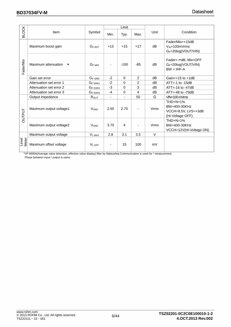
F
ader
/Mix
Maximum boost gain GF BST +13 +15 +17 dB Fader/Mix=+15dB VIN=100mVrms GF=20log(VOUT/VIN)
Maximum attenuation * GF MIN - -100 -85 dB Fader=-∞dB, Mix=OFF GF=20log(VOUT/VIN) BW = IHF-A
Gain set error GF ERR -2 0 2 dB Gain=+15 to +1dB Attenuation set error 1 GF ERR1 -2 0 2 dB ATT=-1 to -15dB Attenuation set error 2 GF ERR2 -3 0 3 dB ATT=-16 to -47dB Attenuation set error 3 GF ERR3 -4 0 4 dB ATT=-48 to -79dB
OU
TP
UT
Output impedance ROUT - - 50 Ω VIN=100 mVrms
Maximum output voltage1 VOM1 2.50 2.75 - Vrms
THD+N=1% BW=400-30KHz VCCH=8.5V, LVS=+3dB (Hi-Voltage OFF)
Maximum output voltage2 VOM2 3.75 4 - Vrms THD+N=1% BW=400-30KHz VCCH=12V(Hi-Voltage ON)
Leve
l M
eter
Maximum output voltage VL MAX 2.8 3.1 3.5 V
Maximum offset voltage VL OFF - 15 100 mV
7/44
DatasheetBD37034FV-M
TSZ02201-0C2C0E100010-1-2
© 2013 ROHM Co., Ltd. All rights reserved. 4.OCT.2013 Rev.002
www.rohm.com
TSZ22111・15・001
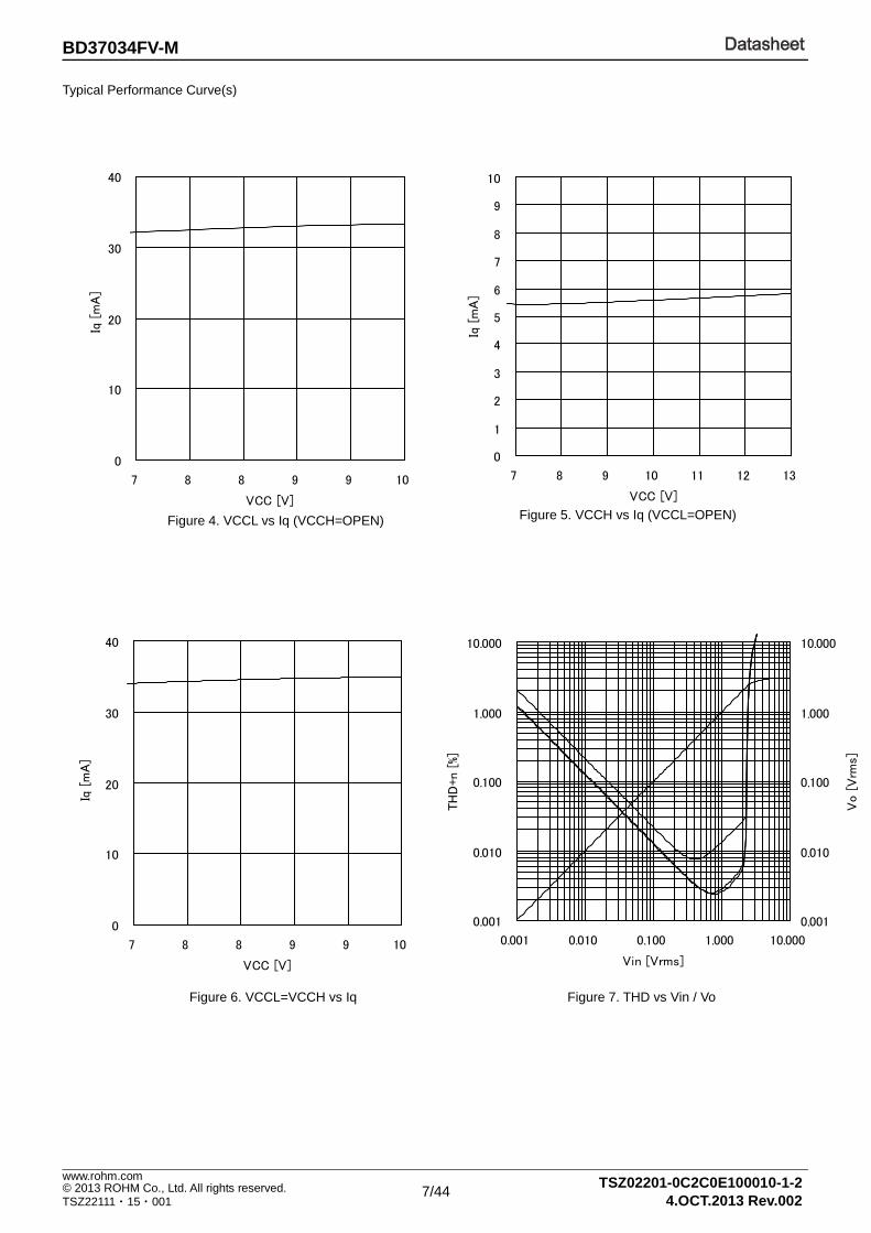
Typical Performance Curve(s)
Figure 6. VCCL=VCCH vs Iq Figure 7. THD vs Vin / Vo
Figure 4. VCCL vs Iq (VCCH=OPEN) Figure 5. VCCH vs Iq (VCCL=OPEN)
0.001
0.010
0.100
1.000
10.000
0.001 0.010 0.100 1.000 10.000
Vin [Vrms]
TH
D+n [%]
0.001
0.010
0.100
1.000
10.000
Vo [V
rm
s]
0
10
20
30
40
7 8 8 9 9 10
VCC [V]
Iq [m
A]
0
10
20
30
40
7 8 8 9 9 10
VCC [V]
Iq [m
A]
0
1
2
3
4
5
6
7
8
9
10
7 8 9 10 11 12 13
VCC [V]
Iq [m
A]
8/44
DatasheetBD37034FV-M
TSZ02201-0C2C0E100010-1-2
© 2013 ROHM Co., Ltd. All rights reserved. 4.OCT.2013 Rev.002
www.rohm.com
TSZ22111・15・001
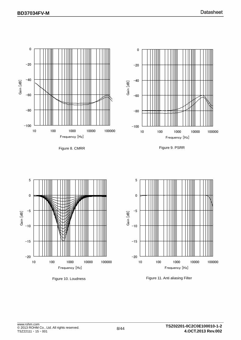
Figure 10. Loudness Figure 11. Anti aliasing Filter
Figure 8. CMRR Figure 9. PSRR
-20
-15
-10
-5
0
5
10 100 1000 10000 100000
Frequency [Hz]
Gain [dB
]
-20
-15
-10
-5
0
5
10 100 1000 10000 100000
Frequency [Hz]
Gain [dB
]-100
-80
-60
-40
-20
0
10 100 1000 10000 100000
Frequency [Hz]
Gain [dB
]
-100
-80
-60
-40
-20
0
10 100 1000 10000 100000
Frequency [Hz]
Gain [dB
]

9/44
DatasheetBD37034FV-M
TSZ02201-0C2C0E100010-1-2
© 2013 ROHM Co., Ltd. All rights reserved. 4.OCT.2013 Rev.002
www.rohm.com
TSZ22111・15・001
Figure 12. Bass gain vs frequency Figure 13. Middle gain vs frequency
Figure 14. Treble gain vs frequency Figure 15. LPF
-100
-80
-60
-40
-20
0
10 100 1000 10000 100000
Frequency [Hz]
Gain [dB
]
-20
-15
-10
-5
0
5
10
15
20
10 100 1000 10000 100000
Frequency [Hz]
Gain [dB
]
-20
-15
-10
-5
0
5
10
15
20
10 100 1000 10000 100000
Frequency [Hz]
Gain [dB
]
-20
-15
-10
-5
0
5
10
15
20
10 100 1000 10000 100000
Frequency [Hz]
Gain [dB
]
10/44
DatasheetBD37034FV-M
TSZ02201-0C2C0E100010-1-2
© 2013 ROHM Co., Ltd. All rights reserved. 4.OCT.2013 Rev.002
www.rohm.com
TSZ22111・15・001
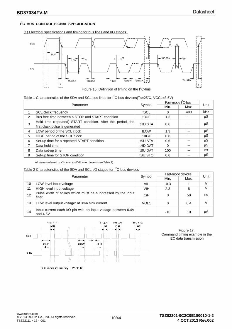
I2C BUS CONTROL SIGNAL SPECIFICATION
(1) Electrical specifications and timing for bus lines and I/O stages
Figure 16. Definition of timing on the I2C-bus
Table 1 Characteristics of the SDA and SCL bus lines for I2C-bus devices(Ta=25, VCCL=8.5V)
Parameter Symbol Fast-mode I2C-bus
Unit Min. Max.
1 SCL clock frequency fSCL 0 400 kHz
2 Bus free time between a STOP and START condition tBUF 1.3 - µS
3 Hold time (repeated) START condition. After this period, the first clock pulse is generated
tHD;STA 0.6 - µS
4 LOW period of the SCL clock tLOW 1.3 - µS
5 HIGH period of the SCL clock tHIGH 0.6 - µS
6 Set-up time for a repeated START condition tSU;STA 0.6 - µS
7 Data hold time tHD;DAT 0 - µS
8 Data set-up time tSU;DAT 100 - ns
9 Set-up time for STOP condition tSU;STO 0.6 - µS
All values referred to VIH min. and VIL max. Levels (see Table 2).
Table 2 Characteristics of the SDA and SCL I/O stages for I2C-bus devices
Parameter Symbol Fast-mode devices
Unit Min. Max.
10 LOW level input voltage VIL -0.3 1 V 11 HIGH level input voltage VIH 2.3 5 V
12 Pulse width of spikes which must be suppressed by the input filter. tSP 0 50 ns
13 LOW level output voltage: at 3mA sink current VOL1 0 0.4 V
14 Input current each I/O pin with an input voltage between 0.4V and 4.5V Ii -10 10 µA
SDA
S
SCL
t
LOW
t
R
t
HD;DAT
P
t
HD;STA
t
HIGH
t
BUF
t
F
t
SU;DAT
t
SU;STA
t
SU;STO
t
SP
t
HD;STA
Sr
P
Figure 17. Command timing example in the
I2C data transmission

11/44
DatasheetBD37034FV-M
TSZ02201-0C2C0E100010-1-2
© 2013 ROHM Co., Ltd. All rights reserved. 4.OCT.2013 Rev.002
www.rohm.com
TSZ22111・15・001
(2)I2C BUS FORMAT MSB LSB MSB LSB MSB LSB
S Slave Address A Select Address A Data A P 1bit 8bit 1bit 8bit 1bit 8bit 1bit 1bit
S = Start conditions (Recognition of start bit) Slave Address = Recognition of slave address. 7 bits in upper order are voluntary.
The least significant bit is “L” due to writing. A = ACKNOWLEDGE bit (Recognition of acknowledgement) Select Address = Select every of volume, bass and treble.
Data = Data on every volume and tone. P = Stop condition (Recognition of stop bit)
(3)I2C BUS Interface Protocol
1)Basic form
S Slave Address A Select Address A Data A P MSB LSB MSB LSB MSB LSB
2)Automatic increment(Select Address increases (+1) according to the number of data)
S Slave Address A Select Address A Data1 A Data2 A ・・・・ DataN A P MSB LSB MSB LSB MSB LSB MSB LSB MSB LSB
(Example)①Data 1 is set as data of Select Address (20h). ②Data 2 is set as data of Select Address +1 (28h). ③Data N is set as data of Select Address +N-1.
3)Configuration unavailable for transmission (In this case, only Select Address 1 is set.) S Slave Address A Select Address1 A Data A Select Address 2 A Data A P
MSB LSB MSB LSB MSB LSB MSB LSB MSB LSB (Note)If any data is transmitted as Select Address 2 next to data,
It is recognized as data, not as Select Address 2. (4)Slave Address
MSB LSB
A6 A5 A4 A3 A2 A1 A0 R/W 1 0 0 0 0 0 0 0
80H

12/44
DatasheetBD37034FV-M
TSZ02201-0C2C0E100010-1-2
© 2013 ROHM Co., Ltd. All rights reserved. 4.OCT.2013 Rev.002
www.rohm.com
TSZ22111・15・001
(5)Select Address and Data
Items Select
Address (hex)
MSB Data LSB
D7 D6 D5 D4 D3 D2 D1 D0
Initial Setup1 01 Advanced
Switch ON/OFF
Anti Alias Filter
ON/OFF
Advanced Switch Time of
Volume/Fader/Mix /Tone/Loudness
Level Shift
Hi-voltage ON/OFF
Advanced Switch Time of Mute
LPF Setup 02 LPF
Phase 0°/180°
Level Meter Reset
Subwoofer Output Selector
Subwoofer Input
Selector1 Subwoofer LPF fc
Initial Setup2 03 Mixing Input Selector
Loudness f0 0 0 Level Meter
ON/OFF
Initial Setup3 04 1ch Mix Input sel
2ch Mix Input sel
Rear Input
Selector
Front Input
Selector
Subwoofer Input Selector2 HPF fc
Input Selector 05 Full-diff Type 0 0 Input Selector
Input Gain 06 MUTE
ON/OFF 0 0 Input Gain
Volume Gain 20 Volume Gain / Attenuation
Fader 1ch Front 28 Fader Gain / Attenuation
Fader 2ch Front 29 Fader Gain / Attenuation
Fader 1ch Rear 2A Fader Gain / Attenuation
Fader 2ch Rear 2B Fader Gain / Attenuation
Fader 1ch Sub 2C Fader Gain / Attenuation
Fader 2ch Sub 2D Fader Gain / Attenuation
Mixing1 Gain 30 Mixing Gain / Attenuation
Mixing2 Gain 31 Mixing Gain / Attenuation
Bass setup 41 0 0 Bass f0 0 0 Bass Q
Middle setup 44 0 0 Middle f0 0 0 Middle Q
Treble setup 47 0 0 Treble f0 0 0 0 Treble Q
Bass Gain 51 Bass Boost/Cut 0 0 Bass Gain
Middle Gain 54 Middle Boost/Cut 0 0 Middle Gain
Treble Gain 57 Treble Boost/Cut 0 0 Treble Gain
Loudness Gain 75 0 HICUT Loudness Gain
Output Level Detector 90 0 0 Threshold
Level Select OUT F1 ON/OFF
OUT F2 ON/OFF
OUT R1 ON/OFF
OUT R2 ON/OFF
Initial Setup4 A0 0 0 0 0 0 0 0 0
Initial Setup5 A1 0 0 0 0 0 0 0 0
Initial Setup6 A2 0 1 0 1 0 0 0 1
Initial Setup7 A3 0 0 1 0 0 0 0 0 System Reset FE 1 0 0 0 0 0 0 1
: Advanced Switch
※(Set up bit (It is written with “0” by the above table) which hasn’t been used in “0”.

13/44
DatasheetBD37034FV-M
TSZ02201-0C2C0E100010-1-2
© 2013 ROHM Co., Ltd. All rights reserved. 4.OCT.2013 Rev.002
www.rohm.com
TSZ22111・15・001
Note 1. In function changing of the hatching part, it works Advanced switch.. 2. Upon continuous data transfer, the Select Address is circulated by the automatic increment function, as shown below.
3. For the function of input selector and subwoofer input select etc, it is not corresponded for advanced switch. Therefore, please apply mute on the side of a set when changes these setting.
4. When using mute function of this IC at the time of changing input selector, please switch mute ON/OFF for waiting advanced-mute time.

14/44
DatasheetBD37034FV-M
TSZ02201-0C2C0E100010-1-2
© 2013 ROHM Co., Ltd. All rights reserved. 4.OCT.2013 Rev.002
www.rohm.com
TSZ22111・15・001
Select address 01(hex) Default:8’ha4
Function Name Mode MSB Initial Setup LSB D7 D6 D5 D4 D3 D2 D1 D0
Advanced Switch Time of Mute
0.6msec
0 0 1.0msec 0 1 1.4msec 1 0 3.2msec 1 1
Hi-voltage ON/OFF
OFF
0
ON 1
Level Shift 0dB
0
+3dB 1
Advanced Switch Time of
Volume /Fader /Tone/Loudness
4.7msec
0 0
7.2msec 0 1 11.2msec 1 0 14.4msec 1 1
Anti Alias Filter ON/OFF
OFF
0
ON 1
Advanced Switch ON/OFF
OFF 0
ON 1
Select address 02(hex) Default:8’h00
Function Name Mode MSB LPF Setup LSB D7 D6 D5 D4 D3 D2 D1 D0
Subwoofer LPF fc
55Hz
0 0 0 85Hz 0 0 1
120Hz 0 1 0 160Hz 0 1 1 PASS 1 0 0
Prohibition 1 0 1 1 1 0 1 1 1
Subwoofer Input Selector1
Loudness
0
Input Selector 1
Subwoofer Output Selector
Subwoofer 1ch(S1/S1)
0 0
Front(F1/F2) 0 1 Rear(R1/R2)
1 0
Subwoofer(S1/S2) 1 1
Level Meter Reset (*1)
Hold
0
Reset 1 LPF Phase 0°/180° (*2)
0° 0
180° 1
: Initial condition (*1): If “Level Meter Reset” is set as Reset(“b1), a reset pulse will be outputted only once to a level meter block. Also about this register, after a reset pulse output returns to a Hold(“b0) state, without holding a Reset(“b1) state. Therefore, in order to change into a Hold state, it is not necessary to carry out a register setup again. (*2): If Subwoofer LPF fc is set as 「PASS」('b000), LPF PHASE is compulsorily fixed to 0°('b0).

15/44
DatasheetBD37034FV-M
TSZ02201-0C2C0E100010-1-2
© 2013 ROHM Co., Ltd. All rights reserved. 4.OCT.2013 Rev.002
www.rohm.com
TSZ22111・15・001
Select address 03(hex) Default:8’h01
Function Name Mode
Pin MSB Initial Setup2 LSB 1p 1n 2n 2p D7 D6 D5 D4 D3 D2 D1 D0
Level Meter ON/OFF(*1)
Output Level Detector Mode
0 Level Meter Mode 1
Loudness f0
400Hz
0 0
800Hz 0 1 2400Hz 1 0
Prohibition 1 1
Mixing Input Selector
(*2)
Mix MIN_EN2 - MIN_E
N2 0 0 0
Prohibition 0 0 1 A_Single A1 - A2 0 1 0
D_Diff DP1 DN DP2 0 1 1 B_Single B1 - B2 1 0 0
E_Diff EP1 EN1 EP2 1 0 1 E_Full-diff EP1 EN
1 MIN_EN2 EP2 1 1 0
Prohibition 1 1 1 (*1): When you use “Output level detector”, please set this register of D0 as 0. Since “Level Meter” and “Output Level Detector” are sharing the terminal, concurrent use is impossible. Default setup is “Level Meter”
D0 16pin 17pin
0 OLDC Filter output terminal of output level detector OLD Output terminal of output
level detector
1 LRST Level meter reset terminal LOUT Output terminal for Level meter
(*2): When you set Mixing Input Selector as “Mix”('b000), please do not set
input Selector(Select Address 05, D0 to D4) as “E_Full_Diff”(’b 01000). When you set Mixing Input Selector as “E_Diff”('b101), please do not set input Selector(Select Address 05, D0 to D4) as “E_Full_Diff”(’b 01000). When you set Mixing Input Selector as “E_Full_Diff”(’b110), please do not set input Selector(Select Address 05, D0 to D4) as “E_Diff”(’b 00111).
Select address 04(hex) Default:8’h80
Function Name Mode MSB HPF Setup LSB D7 D6 D5 D4 D3 D2 D1 D0
HPF fc
55Hz
0 0 85Hz 0 1
120Hz 1 0 160Hz 1 1
Subwoofer Input Selector2
Subwoofer Input Selector1
0 0
LPF ON 0 1 HPF ON 1 0
Prohibition 1 1 Front Input
Selector Loudness
0
HPF ON 1
Rear Input Selector
Loudness
0
HPF ON 1 1ch Mixing
Input Selector 1ch
0
2ch 1
2ch Mixing Input Selector
1ch 0
2ch 1
: Initial condition
16/44
DatasheetBD37034FV-M
TSZ02201-0C2C0E100010-1-2
© 2013 ROHM Co., Ltd. All rights reserved. 4.OCT.2013 Rev.002
www.rohm.com
TSZ22111・15・001
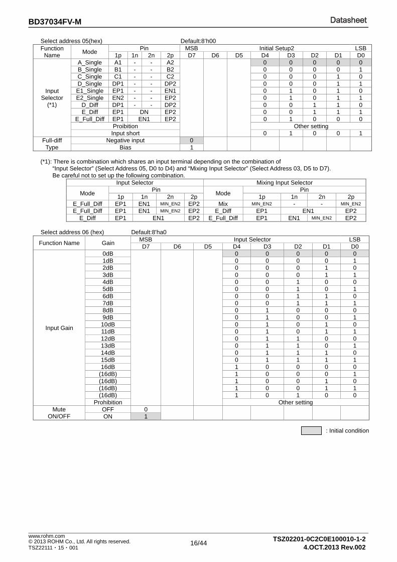
Select address 05(hex) Default:8’h00 Function
Name Mode Pin MSB Initial Setup2 LSB
1p 1n 2n 2p D7 D6 D5 D4 D3 D2 D1 D0
Input Selector
(*1)
A_Single A1 - - A2
0 0 0 0 0 B_Single B1 - - B2 0 0 0 0 1 C_Single C1 - - C2 0 0 0 1 0 D_Single DP1 - - DP2 0 0 0 1 1 E1_Single EP1 - - EN1 0 1 0 1 0 E2_Single EN2 - - EP2 0 1 0 1 1
D_Diff DP1 - - DP2 0 0 1 1 0 E_Diff EP1 DN EP2 0 0 1 1 1
E_Full_Diff EP1 EN1 EP2 0 1 0 0 0 Proibition Other setting Input short 0 1 0 0 1
Full-diff Type
Negative input 0
Bias 1
(*1): There is combination which shares an input terminal depending on the combination of “Input Selector” (Select Address 05, D0 to D4) and “Mixing Input Selector” (Select Address 03, D5 to D7). Be careful not to set up the following combination.
Input Selector Mixing Input Selector
Mode Pin
Mode Pin
1p 1n 2n 2p 1p 1n 2n 2p E_Full_Diff EP1 EN1 MIN_EN2 EP2 Mix MIN_EN2 - - MIN_EN2
E_Full_Diff EP1 EN1 MIN_EN2 EP2 E_Diff EP1 EN1 EP2 E_Diff EP1 EN1 EP2 E_Full_Diff EP1 EN1 MIN_EN2 EP2
Select address 06 (hex) Default:8’ha0
Function Name Gain MSB Input Selector LSB D7 D6 D5 D4 D3 D2 D1 D0
Input Gain
0dB
0 0 0 0 0 1dB 0 0 0 0 1 2dB 0 0 0 1 0 3dB 0 0 0 1 1 4dB 0 0 1 0 0 5dB 0 0 1 0 1 6dB 0 0 1 1 0 7dB 0 0 1 1 1 8dB 0 1 0 0 0 9dB 0 1 0 0 1
10dB 0 1 0 1 0 11dB 0 1 0 1 1 12dB 0 1 1 0 0 13dB 0 1 1 0 1 14dB 0 1 1 1 0 15dB 0 1 1 1 1 16dB 1 0 0 0 0
(16dB) 1 0 0 0 1 (16dB) 1 0 0 1 0 (16dB) 1 0 0 1 1 (16dB) 1 0 1 0 0
Prohibition Other setting Mute
ON/OFF OFF 0
ON 1
: Initial condition
17/44
DatasheetBD37034FV-M
TSZ02201-0C2C0E100010-1-2
© 2013 ROHM Co., Ltd. All rights reserved. 4.OCT.2013 Rev.002
www.rohm.com
TSZ22111・15・001
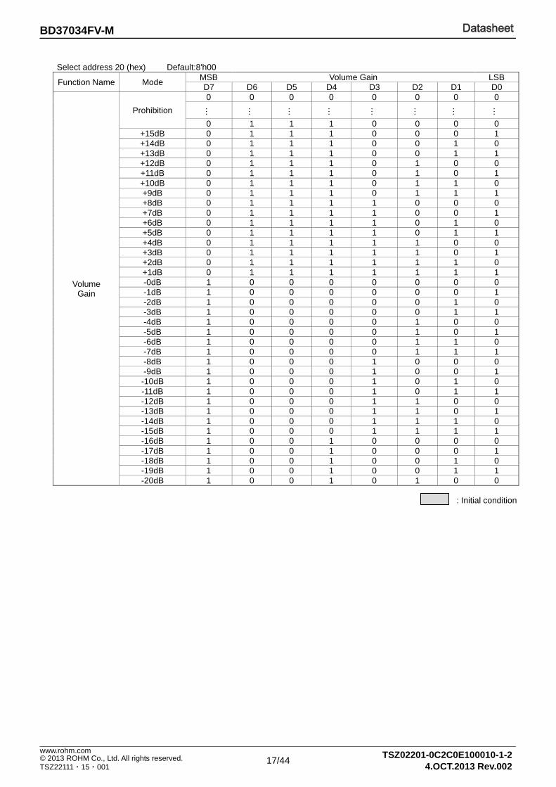
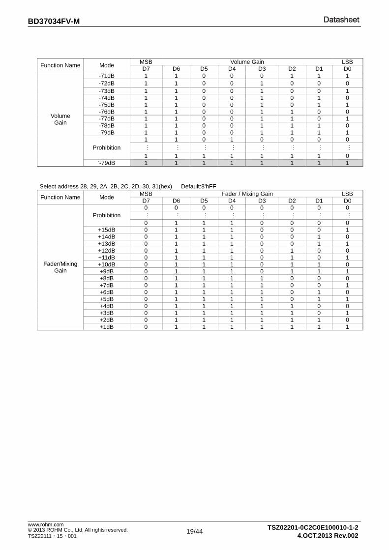
Select address 20 (hex) Default:8'h00
Function Name Mode MSB Volume Gain LSB D7 D6 D5 D4 D3 D2 D1 D0
Volume Gain
Prohibition
0 0 0 0 0 0 0 0
…
…
…
…
…
…
…
…
0 1 1 1 0 0 0 0 +15dB 0 1 1 1 0 0 0 1 +14dB 0 1 1 1 0 0 1 0 +13dB 0 1 1 1 0 0 1 1 +12dB 0 1 1 1 0 1 0 0 +11dB 0 1 1 1 0 1 0 1 +10dB 0 1 1 1 0 1 1 0 +9dB 0 1 1 1 0 1 1 1 +8dB 0 1 1 1 1 0 0 0 +7dB 0 1 1 1 1 0 0 1 +6dB 0 1 1 1 1 0 1 0 +5dB 0 1 1 1 1 0 1 1 +4dB 0 1 1 1 1 1 0 0 +3dB 0 1 1 1 1 1 0 1 +2dB 0 1 1 1 1 1 1 0 +1dB 0 1 1 1 1 1 1 1 -0dB 1 0 0 0 0 0 0 0 -1dB 1 0 0 0 0 0 0 1 -2dB 1 0 0 0 0 0 1 0 -3dB 1 0 0 0 0 0 1 1 -4dB 1 0 0 0 0 1 0 0 -5dB 1 0 0 0 0 1 0 1 -6dB 1 0 0 0 0 1 1 0 -7dB 1 0 0 0 0 1 1 1 -8dB 1 0 0 0 1 0 0 0 -9dB 1 0 0 0 1 0 0 1
-10dB 1 0 0 0 1 0 1 0 -11dB 1 0 0 0 1 0 1 1 -12dB 1 0 0 0 1 1 0 0 -13dB 1 0 0 0 1 1 0 1 -14dB 1 0 0 0 1 1 1 0 -15dB 1 0 0 0 1 1 1 1 -16dB 1 0 0 1 0 0 0 0 -17dB 1 0 0 1 0 0 0 1 -18dB 1 0 0 1 0 0 1 0 -19dB 1 0 0 1 0 0 1 1 -20dB 1 0 0 1 0 1 0 0
: Initial condition
18/44
DatasheetBD37034FV-M
TSZ02201-0C2C0E100010-1-2
© 2013 ROHM Co., Ltd. All rights reserved. 4.OCT.2013 Rev.002
www.rohm.com
TSZ22111・15・001
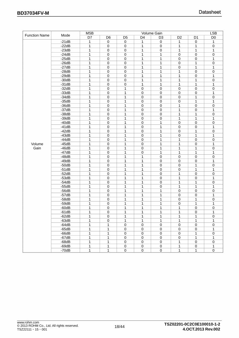
Function Name Mode MSB Volume Gain LSB D7 D6 D5 D4 D3 D2 D1 D0
Volume Gain
-21dB 1 0 0 1 0 1 0 1 -22dB 1 0 0 1 0 1 1 0 -23dB 1 0 0 1 0 1 1 1 -24dB 1 0 0 1 1 0 0 0 -25dB 1 0 0 1 1 0 0 1 -26dB 1 0 0 1 1 0 1 0 -27dB 1 0 0 1 1 0 1 1 -28dB 1 0 0 1 1 1 0 0 -29dB 1 0 0 1 1 1 0 1 -30dB 1 0 0 1 1 1 1 0 -31dB 1 0 0 1 1 1 1 1 -32dB 1 0 1 0 0 0 0 0 -33dB 1 0 1 0 0 0 0 1 -34dB 1 0 1 0 0 0 1 0 -35dB 1 0 1 0 0 0 1 1 -36dB 1 0 1 0 0 1 0 0 -37dB 1 0 1 0 0 1 0 1 -38dB 1 0 1 0 0 1 1 0 -39dB 1 0 1 0 0 1 1 1 -40dB 1 0 1 0 1 0 0 0 -41dB 1 0 1 0 1 0 0 1 -42dB 1 0 1 0 1 0 1 0 -43dB 1 0 1 0 1 0 1 1 -44dB 1 0 1 0 1 1 0 0 -45dB 1 0 1 0 1 1 0 1 -46dB 1 0 1 0 1 1 1 0 -47dB 1 0 1 0 1 1 1 1 -48dB 1 0 1 1 0 0 0 0 -49dB 1 0 1 1 0 0 0 1 -50dB 1 0 1 1 0 0 1 0 -51dB 1 0 1 1 0 0 1 1 -52dB 1 0 1 1 0 1 0 0 -53dB 1 0 1 1 0 1 0 1 -54dB 1 0 1 1 0 1 1 0 -55dB 1 0 1 1 0 1 1 1 -56dB 1 0 1 1 1 0 0 0 -57dB 1 0 1 1 1 0 0 1 -58dB 1 0 1 1 1 0 1 0 -59dB 1 0 1 1 1 0 1 1 -60dB 1 0 1 1 1 1 0 0 -61dB 1 0 1 1 1 1 0 1 -62dB 1 0 1 1 1 1 1 0 -63dB 1 0 1 1 1 1 1 1 -64dB 1 1 0 0 0 0 0 0 -65dB 1 1 0 0 0 0 0 1 -66dB 1 1 0 0 0 0 1 0 -67dB 1 1 0 0 0 0 1 1 -68dB 1 1 0 0 0 1 0 0 -69dB 1 1 0 0 0 1 0 1 -70dB 1 1 0 0 0 1 1 0
19/44
DatasheetBD37034FV-M
TSZ02201-0C2C0E100010-1-2
© 2013 ROHM Co., Ltd. All rights reserved. 4.OCT.2013 Rev.002
www.rohm.com
TSZ22111・15・001
Function Name Mode MSB Volume Gain LSB D7 D6 D5 D4 D3 D2 D1 D0
Volume Gain
-71dB 1 1 0 0 0 1 1 1 -72dB 1 1 0 0 1 0 0 0 -73dB 1 1 0 0 1 0 0 1 -74dB 1 1 0 0 1 0 1 0 -75dB 1 1 0 0 1 0 1 1 -76dB 1 1 0 0 1 1 0 0 -77dB 1 1 0 0 1 1 0 1 -78dB 1 1 0 0 1 1 1 0 -79dB 1 1 0 0 1 1 1 1
Prohibition 1 1 0 1 0 0 0 0
…
…
…
…
…
…
…
…
1 1 1 1 1 1 1 0 '-79dB 1 1 1 1 1 1 1 1
Select address 28, 29, 2A, 2B, 2C, 2D, 30, 31(hex) Default:8'hFF
Function Name Mode MSB Fader / Mixing Gain LSB D7 D6 D5 D4 D3 D2 D1 D0
Fader/Mixing Gain
Prohibition 0 0 0 0 0 0 0 0
…
…
…
…
…
…
…
…
0 1 1 1 0 0 0 0 +15dB 0 1 1 1 0 0 0 1 +14dB 0 1 1 1 0 0 1 0 +13dB 0 1 1 1 0 0 1 1 +12dB 0 1 1 1 0 1 0 0 +11dB 0 1 1 1 0 1 0 1 +10dB 0 1 1 1 0 1 1 0 +9dB 0 1 1 1 0 1 1 1 +8dB 0 1 1 1 1 0 0 0 +7dB 0 1 1 1 1 0 0 1 +6dB 0 1 1 1 1 0 1 0 +5dB 0 1 1 1 1 0 1 1 +4dB 0 1 1 1 1 1 0 0 +3dB 0 1 1 1 1 1 0 1 +2dB 0 1 1 1 1 1 1 0 +1dB 0 1 1 1 1 1 1 1
20/44
DatasheetBD37034FV-M
TSZ02201-0C2C0E100010-1-2
© 2013 ROHM Co., Ltd. All rights reserved. 4.OCT.2013 Rev.002
www.rohm.com
TSZ22111・15・001
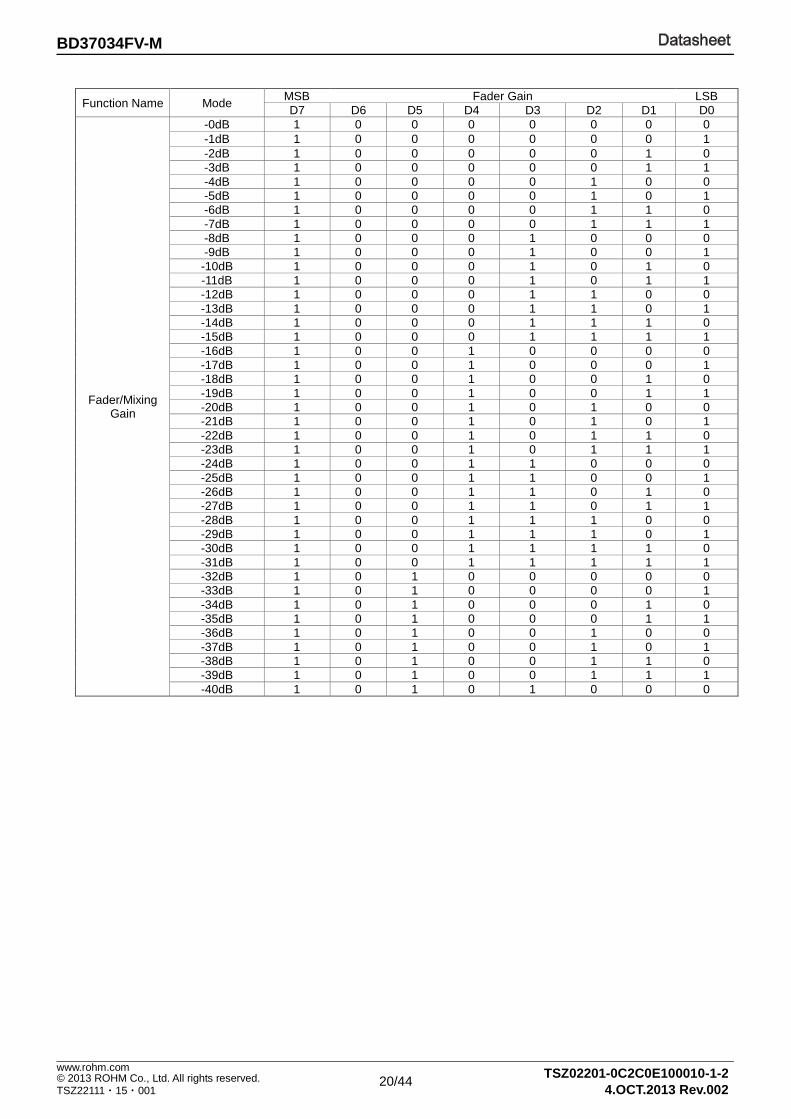
Function Name Mode MSB Fader Gain LSB D7 D6 D5 D4 D3 D2 D1 D0
Fader/Mixing Gain
-0dB 1 0 0 0 0 0 0 0 -1dB 1 0 0 0 0 0 0 1 -2dB 1 0 0 0 0 0 1 0 -3dB 1 0 0 0 0 0 1 1 -4dB 1 0 0 0 0 1 0 0 -5dB 1 0 0 0 0 1 0 1 -6dB 1 0 0 0 0 1 1 0 -7dB 1 0 0 0 0 1 1 1 -8dB 1 0 0 0 1 0 0 0 -9dB 1 0 0 0 1 0 0 1
-10dB 1 0 0 0 1 0 1 0 -11dB 1 0 0 0 1 0 1 1 -12dB 1 0 0 0 1 1 0 0 -13dB 1 0 0 0 1 1 0 1 -14dB 1 0 0 0 1 1 1 0 -15dB 1 0 0 0 1 1 1 1 -16dB 1 0 0 1 0 0 0 0 -17dB 1 0 0 1 0 0 0 1 -18dB 1 0 0 1 0 0 1 0 -19dB 1 0 0 1 0 0 1 1 -20dB 1 0 0 1 0 1 0 0 -21dB 1 0 0 1 0 1 0 1 -22dB 1 0 0 1 0 1 1 0 -23dB 1 0 0 1 0 1 1 1 -24dB 1 0 0 1 1 0 0 0 -25dB 1 0 0 1 1 0 0 1 -26dB 1 0 0 1 1 0 1 0 -27dB 1 0 0 1 1 0 1 1 -28dB 1 0 0 1 1 1 0 0 -29dB 1 0 0 1 1 1 0 1 -30dB 1 0 0 1 1 1 1 0 -31dB 1 0 0 1 1 1 1 1 -32dB 1 0 1 0 0 0 0 0 -33dB 1 0 1 0 0 0 0 1 -34dB 1 0 1 0 0 0 1 0 -35dB 1 0 1 0 0 0 1 1 -36dB 1 0 1 0 0 1 0 0 -37dB 1 0 1 0 0 1 0 1 -38dB 1 0 1 0 0 1 1 0 -39dB 1 0 1 0 0 1 1 1 -40dB 1 0 1 0 1 0 0 0
21/44
DatasheetBD37034FV-M
TSZ02201-0C2C0E100010-1-2
© 2013 ROHM Co., Ltd. All rights reserved. 4.OCT.2013 Rev.002
www.rohm.com
TSZ22111・15・001
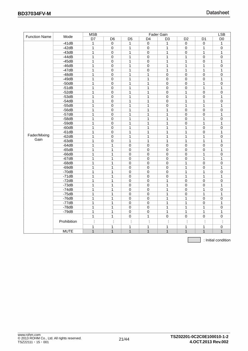
Function Name Mode MSB Fader Gain LSB D7 D6 D5 D4 D3 D2 D1 D0
Fader/Mixing Gain
-41dB 1 0 1 0 1 0 0 1 -42dB 1 0 1 0 1 0 1 0 -43dB 1 0 1 0 1 0 1 1 -44dB 1 0 1 0 1 1 0 0 -45dB 1 0 1 0 1 1 0 1 -46dB 1 0 1 0 1 1 1 0 -47dB 1 0 1 0 1 1 1 1 -48dB 1 0 1 1 0 0 0 0 -49dB 1 0 1 1 0 0 0 1 -50dB 1 0 1 1 0 0 1 0 -51dB 1 0 1 1 0 0 1 1 -52dB 1 0 1 1 0 1 0 0 -53dB 1 0 1 1 0 1 0 1 -54dB 1 0 1 1 0 1 1 0 -55dB 1 0 1 1 0 1 1 1 -56dB 1 0 1 1 1 0 0 0 -57dB 1 0 1 1 1 0 0 1 -58dB 1 0 1 1 1 0 1 0 -59dB 1 0 1 1 1 0 1 1 -60dB 1 0 1 1 1 1 0 0 -61dB 1 0 1 1 1 1 0 1 -62dB 1 0 1 1 1 1 1 0 -63dB 1 0 1 1 1 1 1 1 -64dB 1 1 0 0 0 0 0 0 -65dB 1 1 0 0 0 0 0 1 -66dB 1 1 0 0 0 0 1 0 -67dB 1 1 0 0 0 0 1 1 -68dB 1 1 0 0 0 1 0 0 -69dB 1 1 0 0 0 1 0 1 -70dB 1 1 0 0 0 1 1 0 -71dB 1 1 0 0 0 1 1 1 -72dB 1 1 0 0 1 0 0 0 -73dB 1 1 0 0 1 0 0 1 -74dB 1 1 0 0 1 0 1 0 -75dB 1 1 0 0 1 0 1 1 -76dB 1 1 0 0 1 1 0 0 -77dB 1 1 0 0 1 1 0 1 -78dB 1 1 0 0 1 1 1 0 -79dB 1 1 0 0 1 1 1 1
Prohibition 1 1 0 1 0 0 0 0
…
…
…
…
…
…
…
…
1 1 1 1 1 1 1 0 MUTE 1 1 1 1 1 1 1 1
: Initial condition

22/44
DatasheetBD37034FV-M
TSZ02201-0C2C0E100010-1-2
© 2013 ROHM Co., Ltd. All rights reserved. 4.OCT.2013 Rev.002
www.rohm.com
TSZ22111・15・001
Select address 41(hex) Default:8’h00
Function Name Mode MSB Bass setup LSB D7 D6 D5 D4 D3 D2 D1 D0
Bass Q
0.5
0 0 1.0 0 1 1.5 1 0 2.0 1 1
Bass f0
60Hz
0 0
80Hz 0 1
100Hz 1 0 120Hz 1 1
Select address 44(hex) Default:8’h00
Function Name Mode MSB Middle setup LSB D7 D6 D5 D4 D3 D2 D1 D0
Middle Q
0.75
0 0 1.00 0 1 1.25 1 0 1.50 1 1
Middle f0
0.5kHz
0 0
1kHz 0 1
1.5kHz 1 0 2.5kHz 1 1
Select address 47(hex) Default:8’h00
Function Name Mode MSB Treble setup LSB D7 D6 D5 D4 D3 D2 D1 D0
Treble Q 0.75
0
1.25 1
Treble f0
7.5kHz
0 0
10kHz 0 1
12.5kHz 1 0 15kHz 1 1
: Initial condition
23/44
DatasheetBD37034FV-M
TSZ02201-0C2C0E100010-1-2
© 2013 ROHM Co., Ltd. All rights reserved. 4.OCT.2013 Rev.002
www.rohm.com
TSZ22111・15・001
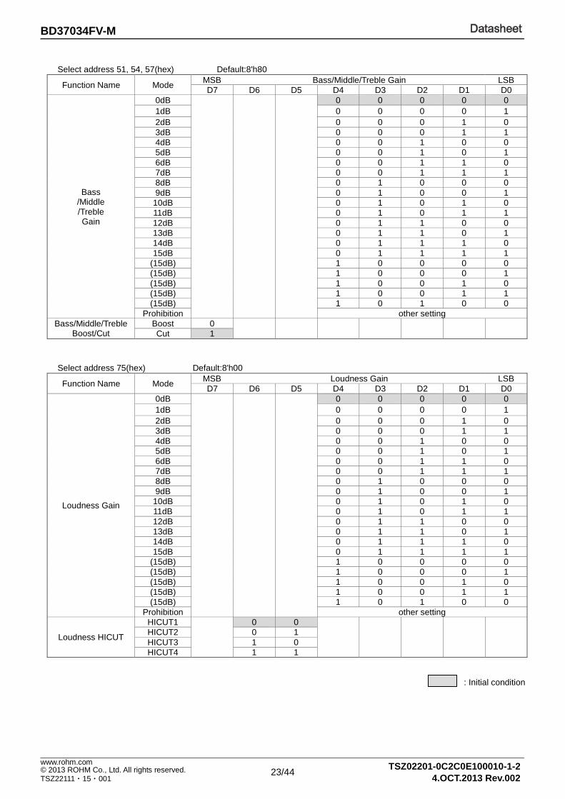
Select address 51, 54, 57(hex) Default:8'h80
Function Name Mode MSB Bass/Middle/Treble Gain LSB D7 D6 D5 D4 D3 D2 D1 D0
Bass /Middle /Treble Gain
0dB
0 0 0 0 0 1dB 0 0 0 0 1 2dB 0 0 0 1 0 3dB 0 0 0 1 1 4dB 0 0 1 0 0 5dB 0 0 1 0 1 6dB 0 0 1 1 0 7dB 0 0 1 1 1 8dB 0 1 0 0 0 9dB 0 1 0 0 1
10dB 0 1 0 1 0 11dB 0 1 0 1 1 12dB 0 1 1 0 0 13dB 0 1 1 0 1 14dB 0 1 1 1 0 15dB 0 1 1 1 1
(15dB) 1 0 0 0 0 (15dB) 1 0 0 0 1 (15dB) 1 0 0 1 0 (15dB) 1 0 0 1 1 (15dB) 1 0 1 0 0
Prohibition other setting Bass/Middle/Treble
Boost/Cut Boost 0
Cut 1
Select address 75(hex) Default:8'h00
Function Name Mode MSB Loudness Gain LSB D7 D6 D5 D4 D3 D2 D1 D0
Loudness Gain
0dB
0 0 0 0 0 1dB 0 0 0 0 1 2dB 0 0 0 1 0 3dB 0 0 0 1 1 4dB 0 0 1 0 0 5dB 0 0 1 0 1 6dB 0 0 1 1 0 7dB 0 0 1 1 1 8dB 0 1 0 0 0 9dB 0 1 0 0 1
10dB 0 1 0 1 0 11dB 0 1 0 1 1 12dB 0 1 1 0 0 13dB 0 1 1 0 1 14dB 0 1 1 1 0 15dB 0 1 1 1 1
(15dB) 1 0 0 0 0 (15dB) 1 0 0 0 1 (15dB) 1 0 0 1 0 (15dB) 1 0 0 1 1 (15dB) 1 0 1 0 0
Prohibition other setting
Loudness HICUT
HICUT1
0 0
HICUT2 0 1 HICUT3 1 0 HICUT4 1 1
: Initial condition
24/44
DatasheetBD37034FV-M
TSZ02201-0C2C0E100010-1-2
© 2013 ROHM Co., Ltd. All rights reserved. 4.OCT.2013 Rev.002
www.rohm.com
TSZ22111・15・001
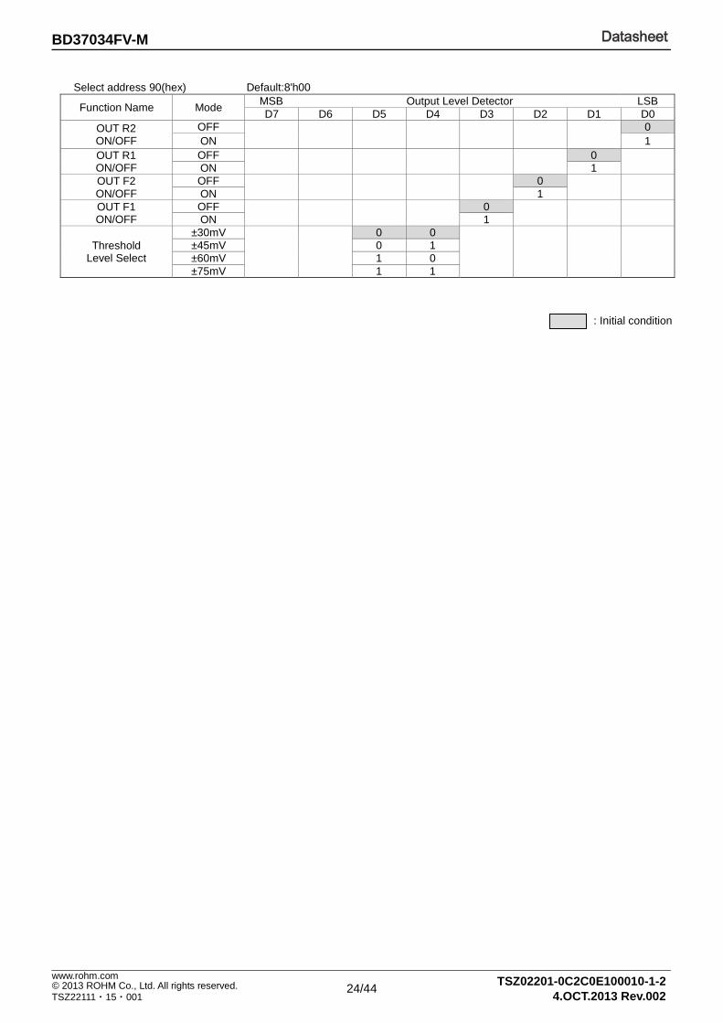
Select address 90(hex) Default:8'h00
Function Name Mode MSB Output Level Detector LSB D7 D6 D5 D4 D3 D2 D1 D0
OUT R2 ON/OFF
OFF
0 ON 1
OUT R1 ON/OFF
OFF
0
ON 1 OUT F2 ON/OFF
OFF
0
ON 1 OUT F1 ON/OFF
OFF
0
ON 1
Threshold Level Select
±30mV
0 0
±45mV 0 1 ±60mV 1 0 ±75mV 1 1
: Initial condition
25/44
DatasheetBD37034FV-M
TSZ02201-0C2C0E100010-1-2
© 2013 ROHM Co., Ltd. All rights reserved. 4.OCT.2013 Rev.002
www.rohm.com
TSZ22111・15・001
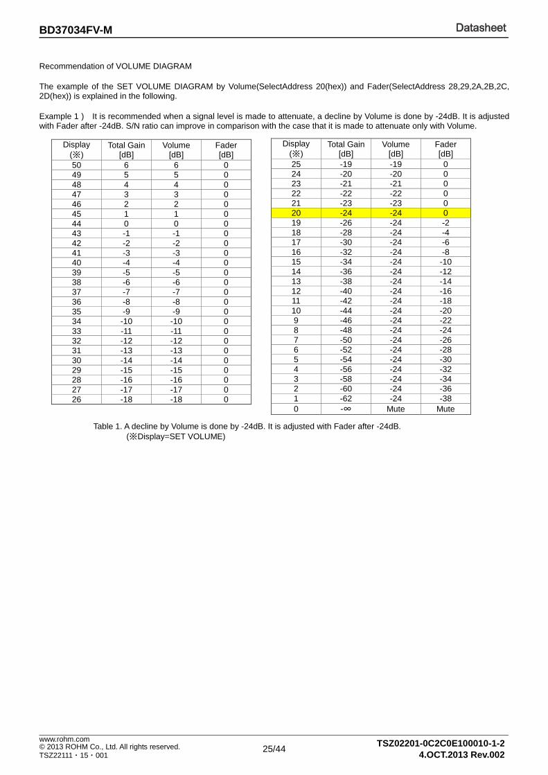
Recommendation of VOLUME DIAGRAM
The example of the SET VOLUME DIAGRAM by Volume(SelectAddress 20(hex)) and Fader(SelectAddress 28,29,2A,2B,2C, 2D(hex)) is explained in the following.
Example 1 ) It is recommended when a signal level is made to attenuate, a decline by Volume is done by -24dB. It is adjusted with Fader after -24dB. S/N ratio can improve in comparison with the case that it is made to attenuate only with Volume.
Table 1. A decline by Volume is done by -24dB. It is adjusted with Fader after -24dB. (※Display=SET VOLUME)
Display (※)
Total Gain [dB]
Volume [dB]
Fader [dB]
50 6 6 0 49 5 5 0 48 4 4 0 47 3 3 0 46 2 2 0 45 1 1 0 44 0 0 0 43 -1 -1 0 42 -2 -2 0 41 -3 -3 0 40 -4 -4 0 39 -5 -5 0 38 -6 -6 0 37 -7 -7 0 36 -8 -8 0 35 -9 -9 0 34 -10 -10 0 33 -11 -11 0 32 -12 -12 0 31 -13 -13 0 30 -14 -14 0 29 -15 -15 0 28 -16 -16 0 27 -17 -17 0 26 -18 -18 0
Display (※)
Total Gain [dB]
Volume [dB]
Fader [dB]
25 -19 -19 0 24 -20 -20 0 23 -21 -21 0 22 -22 -22 0 21 -23 -23 0 20 -24 -24 0 19 -26 -24 -2 18 -28 -24 -4 17 -30 -24 -6 16 -32 -24 -8 15 -34 -24 -10 14 -36 -24 -12 13 -38 -24 -14 12 -40 -24 -16 11 -42 -24 -18 10 -44 -24 -20 9 -46 -24 -22 8 -48 -24 -24 7 -50 -24 -26 6 -52 -24 -28 5 -54 -24 -30 4 -56 -24 -32 3 -58 -24 -34 2 -60 -24 -36 1 -62 -24 -38 0 -∞ Mute Mute
26/44
DatasheetBD37034FV-M
TSZ02201-0C2C0E100010-1-2
© 2013 ROHM Co., Ltd. All rights reserved. 4.OCT.2013 Rev.002
www.rohm.com
TSZ22111・15・001
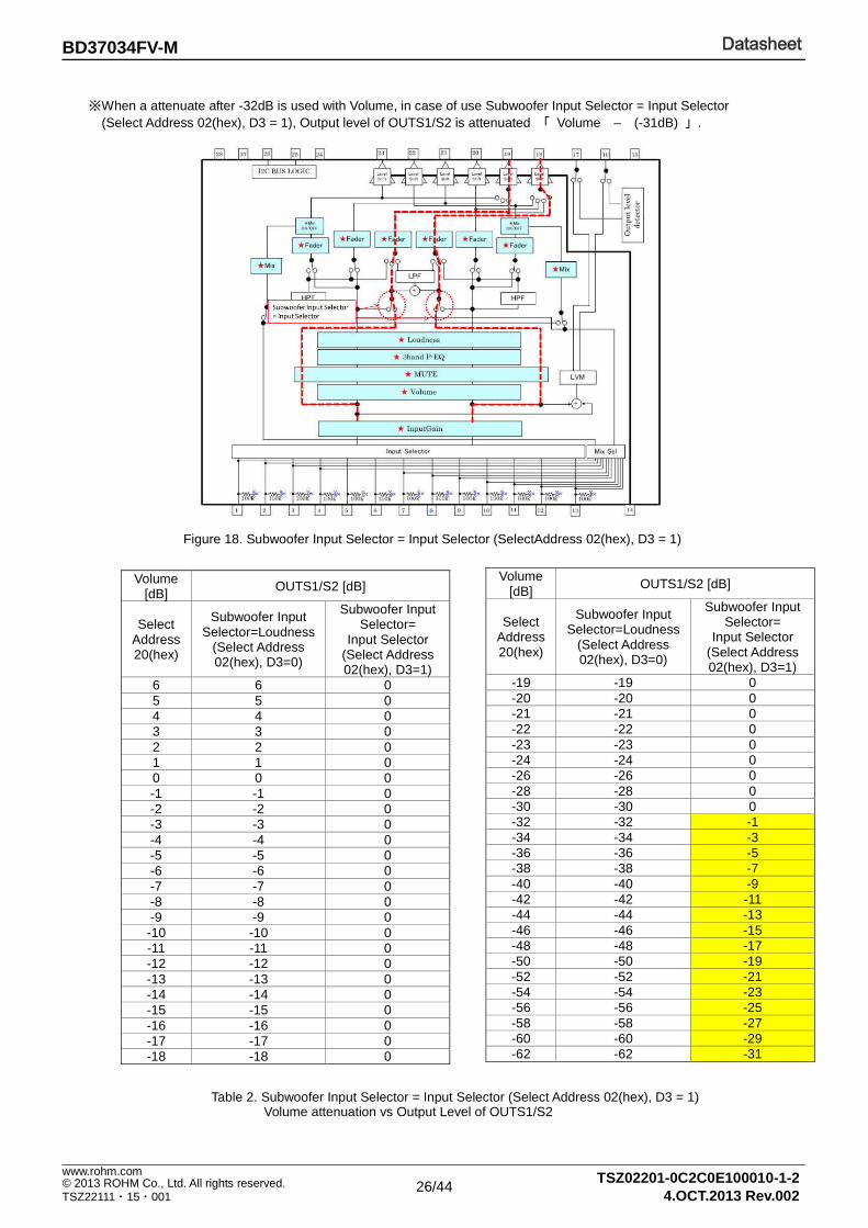
※When a attenuate after -32dB is used with Volume, in case of use Subwoofer Input Selector = Input Selector
(Select Address 02(hex), D3 = 1), Output level of OUTS1/S2 is attenuated 「 Volume – (-31dB) 」.
Volume [dB] OUTS1/S2 [dB]
Select Address 20(hex)
Subwoofer Input Selector=Loudness
(Select Address 02(hex), D3=0)
Subwoofer Input Selector=
Input Selector (Select Address 02(hex), D3=1)
6 6 0 5 5 0 4 4 0 3 3 0 2 2 0 1 1 0 0 0 0 -1 -1 0 -2 -2 0 -3 -3 0 -4 -4 0 -5 -5 0 -6 -6 0 -7 -7 0 -8 -8 0 -9 -9 0 -10 -10 0 -11 -11 0 -12 -12 0 -13 -13 0 -14 -14 0 -15 -15 0 -16 -16 0 -17 -17 0 -18 -18 0
Volume [dB] OUTS1/S2 [dB]
Select Address 20(hex)
Subwoofer Input Selector=Loudness
(Select Address 02(hex), D3=0)
Subwoofer Input Selector=
Input Selector (Select Address 02(hex), D3=1)
-19 -19 0 -20 -20 0 -21 -21 0 -22 -22 0 -23 -23 0 -24 -24 0 -26 -26 0 -28 -28 0 -30 -30 0 -32 -32 -1 -34 -34 -3 -36 -36 -5 -38 -38 -7 -40 -40 -9 -42 -42 -11 -44 -44 -13 -46 -46 -15 -48 -48 -17 -50 -50 -19 -52 -52 -21 -54 -54 -23 -56 -56 -25 -58 -58 -27 -60 -60 -29 -62 -62 -31
Figure 18. Subwoofer Input Selector = Input Selector (SelectAddress 02(hex), D3 = 1)
Table 2. Subwoofer Input Selector = Input Selector (Select Address 02(hex), D3 = 1) Volume attenuation vs Output Level of OUTS1/S2
27/44
DatasheetBD37034FV-M
TSZ02201-0C2C0E100010-1-2
© 2013 ROHM Co., Ltd. All rights reserved. 4.OCT.2013 Rev.002
www.rohm.com
TSZ22111・15・001
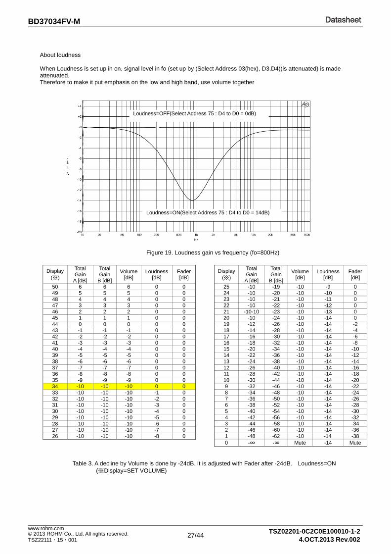
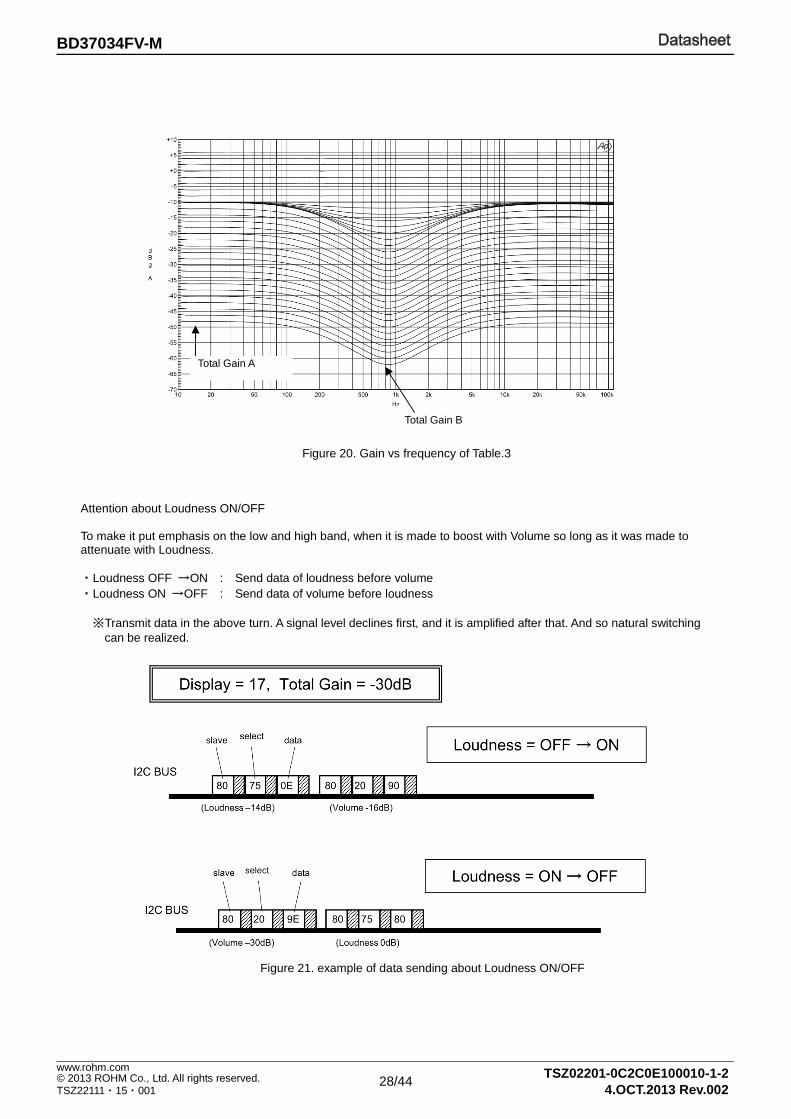
About loudness When Loudness is set up in on, signal level in fo (set up by (Select Address 03(hex), D3,D4))is attenuated) is made attenuated. Therefore to make it put emphasis on the low and high band, use volume together
Figure 19. Loudness gain vs frequency (fo=800Hz)
Table 3. A decline by Volume is done by -24dB. It is adjusted with Fader after -24dB. Loudness=ON (※Display=SET VOLUME)
Display (※)
Total Gain
A [dB]
Total Gain
B [dB]
Volume [dB]
Loudness [dB]
Fader [dB]
25 -10 -19 -10 -9 0 24 -10 -20 -10 -10 0 23 -10 -21 -10 -11 0 22 -10 -22 -10 -12 0 21 -10-10 -23 -10 -13 0 20 -10 -24 -10 -14 0 19 -12 -26 -10 -14 -2 18 -14 -28 -10 -14 -4 17 -16 -30 -10 -14 -6 16 -18 -32 -10 -14 -8 15 -20 -34 -10 -14 -10 14 -22 -36 -10 -14 -12 13 -24 -38 -10 -14 -14 12 -26 -40 -10 -14 -16 11 -28 -42 -10 -14 -18 10 -30 -44 -10 -14 -20 9 -32 -46 -10 -14 -22 8 -34 -48 -10 -14 -24 7 -36 -50 -10 -14 -26 6 -38 -52 -10 -14 -28 5 -40 -54 -10 -14 -30 4 -42 -56 -10 -14 -32 3 -44 -58 -10 -14 -34 2 -46 -60 -10 -14 -36 1 -48 -62 -10 -14 -38 0 -∞ -∞ Mute -14 Mute
Display (※)
Total Gain
A [dB]
Total Gain
B [dB]
Volume [dB]
Loudness [dB]
Fader [dB]
50 6 6 6 0 0 49 5 5 5 0 0 48 4 4 4 0 0 47 3 3 3 0 0 46 2 2 2 0 0 45 1 1 1 0 0 44 0 0 0 0 0 43 -1 -1 -1 0 0 42 -2 -2 -2 0 0 41 -3 -3 -3 0 0 40 -4 -4 -4 0 0 39 -5 -5 -5 0 0 38 -6 -6 -6 0 0 37 -7 -7 -7 0 0 36 -8 -8 -8 0 0 35 -9 -9 -9 0 0 34 -10 -10 -10 0 0 33 -10 -10 -10 -1 0 32 -10 -10 -10 -2 0 31 -10 -10 -10 -3 0 30 -10 -10 -10 -4 0 29 -10 -10 -10 -5 0 28 -10 -10 -10 -6 0 27 -10 -10 -10 -7 0 26 -10 -10 -10 -8 0
Loudness=OFF(Select Address 75 : D4 to D0 = 0dB)
Loudness=ON(Select Address 75 : D4 to D0 = 14dB)
28/44
DatasheetBD37034FV-M
TSZ02201-0C2C0E100010-1-2
© 2013 ROHM Co., Ltd. All rights reserved. 4.OCT.2013 Rev.002
www.rohm.com
TSZ22111・15・001
Figure 20. Gain vs frequency of Table.3
Attention about Loudness ON/OFF To make it put emphasis on the low and high band, when it is made to boost with Volume so long as it was made to attenuate with Loudness. ・Loudness OFF →ON : Send data of loudness before volume ・Loudness ON →OFF : Send data of volume before loudness
※Transmit data in the above turn. A signal level declines first, and it is amplified after that. And so natural switching can be realized.
Figure 21. example of data sending about Loudness ON/OFF
Total Gain B
Total Gain A
29/44
DatasheetBD37034FV-M
TSZ02201-0C2C0E100010-1-2
© 2013 ROHM Co., Ltd. All rights reserved. 4.OCT.2013 Rev.002
www.rohm.com
TSZ22111・15・001
(6)About power on reset At on of supply voltage circuit made initialization inside IC is built-in. Please send data to all address as initial data at supply voltage on. And please supply mute at set side until this initial data is sent.)
Item Symbol Limit
Unit Condition Min. Typ. Max.
Rise time of VCCL Trise 33 - - usec VCCL rise time from 0V to 5V) VCCL voltage of release power on reset Vpor - 4.1 - V
(7)About external compulsory mute terminal
Mute is possible forcibly than the outside after input again department, by the setting of the MUTE terminal.
Mute Voltage Condition Mode
GND to 1.0V MUTE ON 2.3V to 5.0V MUTE OFF
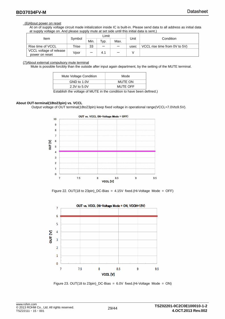
Establish the voltage of MUTE in the condition to have been defined.) About OUT-terminal(18to23pin) vs. VCCL
Output voltage of OUT terminal(18to23pin) keep fixed voltage in operational range(VCCL=7.0Vto9.5V).
Figure 22. OUT(18 to 23pin)_DC-Bias = 4.15V fixed.(Hi-Voltage Mode = OFF)
Figure 23. OUT(18 to 23pin)_DC-Bias = 6.0V fixed.(Hi-Voltage Mode = ON)
30/44
DatasheetBD37034FV-M
TSZ02201-0C2C0E100010-1-2
© 2013 ROHM Co., Ltd. All rights reserved. 4.OCT.2013 Rev.002
www.rohm.com
TSZ22111・15・001
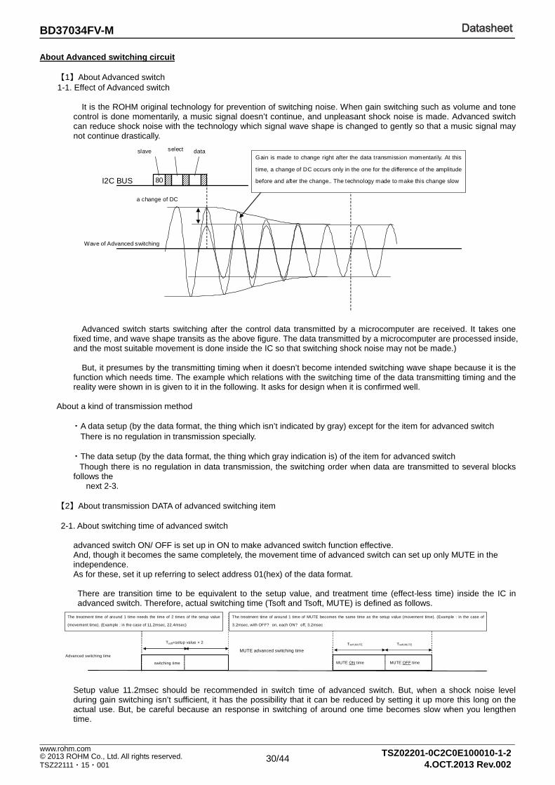
About Advanced switching circuit 【1】About Advanced switch 1-1. Effect of Advanced switch
It is the ROHM original technology for prevention of switching noise. When gain switching such as volume and tone
control is done momentarily, a music signal doesn’t continue, and unpleasant shock noise is made. Advanced switch can reduce shock noise with the technology which signal wave shape is changed to gently so that a music signal may not continue drastically.
Advanced switch starts switching after the control data transmitted by a microcomputer are received. It takes one fixed time, and wave shape transits as the above figure. The data transmitted by a microcomputer are processed inside, and the most suitable movement is done inside the IC so that switching shock noise may not be made.)
But, it presumes by the transmitting timing when it doesn’t become intended switching wave shape because it is the
function which needs time. The example which relations with the switching time of the data transmitting timing and the reality were shown in is given to it in the following. It asks for design when it is confirmed well.
About a kind of transmission method
・A data setup (by the data format, the thing which isn’t indicated by gray) except for the item for advanced switch
There is no regulation in transmission specially.
・The data setup (by the data format, the thing which gray indication is) of the item for advanced switch Though there is no regulation in data transmission, the switching order when data are transmitted to several blocks follows the
next 2-3.
【2】About transmission DATA of advanced switching item 2-1. About switching time of advanced switch
advanced switch ON/ OFF is set up in ON to make advanced switch function effective. And, though it becomes the same completely, the movement time of advanced switch can set up only MUTE in the independence. As for these, set it up referring to select address 01(hex) of the data format.
There are transition time to be equivalent to the setup value, and treatment time (effect-less time) inside the IC in advanced switch. Therefore, actual switching time (Tsoft and Tsoft, MUTE) is defined as follows.
Setup value 11.2msec should be recommended in switch time of advanced switch. But, when a shock noise level during gain switching isn’t sufficient, it has the possibility that it can be reduced by setting it up more this long on the actual use. But, be careful because an response in switching of around one time becomes slow when you lengthen time.
Gain is made to change right after the data transmission momentarily. At this
t ime, a change of DC occurs only in the one for the difference of the amplitude
before and after the change.. The technology made to make this change slow
a change of DC
80 I2C BUS
Wave of Advanced switching
slave select data
switching time
Advanced switching time
Tsoft=setup value × 2
The treatment time of around 1 time needs the time of 2 times of the setup value
(movement time). (Example : in the case of 11.2msec, 22.4msec)
MUTE ON time
Tsoft,MUTE
The treatment time of around 1 time of MUTE becomes the same time as the setup value (movement time). (Example : in the case of
3.2msec, with OFF? on, each ON? off, 3.2msec
MUTE OFF time
Tsoft,MUTE
MUTE advanced switching time
31/44
DatasheetBD37034FV-M
TSZ02201-0C2C0E100010-1-2
© 2013 ROHM Co., Ltd. All rights reserved. 4.OCT.2013 Rev.002
www.rohm.com
TSZ22111・15・001
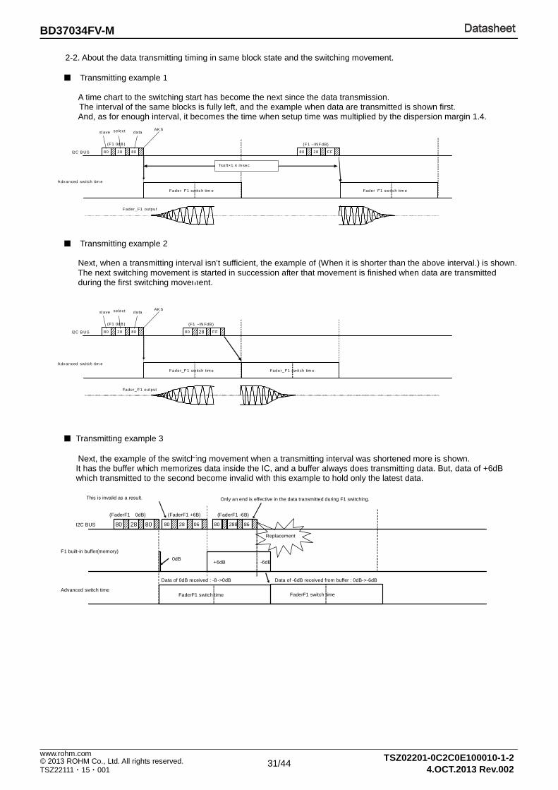
2-2. About the data transmitting timing in same block state and the switching movement.
Transmitting example 1
A time chart to the switching start has become the next since the data transmission. The interval of the same blocks is fully left, and the example when data are transmitted is shown first.
And, as for enough interval, it becomes the time when setup time was multiplied by the dispersion margin 1.4.
Transmitting example 2
Next, when a transmitting interval isn’t sufficient, the example of (When it is shorter than the above interval.) is shown. The next switching movement is started in succession after that movement is finished when data are transmitted during the first switching movement.
Transmitting example 3
Next, the example of the switching movement when a transmitting interval was shortened more is shown. It has the buffer which memorizes data inside the IC, and a buffer always does transmitting data. But, data of +6dB which transmitted to the second become invalid with this example to hold only the latest data.
80 28 80
Fade r F1 switc h tim e
I2C B US
A dv anced switch tim e
(F1 0dB )
slave select da ta AK S
Fader_F1 output
80 28 FF
(F1 –INFdB)
Tsoft×1.4 m sec
Fader F1 switch tim e
80 28 80
Fade r_F 1 switch tim e
I2C B US
A dv anced switch tim e
(F1 0dB )
slave select da ta AK S
Fader_F1 out put
80 28 FF
(F1 –IN FdB)
Fader_F1 switch tim e
Data of -6dB received from buffer : 0dB->-6dB
80 28 80 80 28 06 80 288 86
+6dB
I2C BUS
F1 built-in buffer(memory)
(FaderF1 0dB) (FaderF1 +6B) (FaderF1 -6B)
This is invalid as a result. Only an end is effective in the data transmitted during F1 switching.
FaderF1 switch time Advanced switch time
-6dB
Data of 0dB received : -8 ->0dB
0dB
Replacement
FaderF1 switch time

32/44
DatasheetBD37034FV-M
TSZ02201-0C2C0E100010-1-2
© 2013 ROHM Co., Ltd. All rights reserved. 4.OCT.2013 Rev.002
www.rohm.com
TSZ22111・15・001
Transmitting example 4 As for handling of refresh-data, advanced switch movement isn’t started to judge for present setup data and a difference that to be inside the IC)
2-3. About the data transmitting timing in several block state and the switching movement.)
When data are transmitted to several blocks, treatment in the BS (block state) unit is carried out inside the IC. The movement start order of advanced switch is decided by BS in advance.)
Figure 24. The order of advanced switch start
※It is possible in the block in the same BS that switching is started at the same timing.
Transmitting example 5 The timing of the switching start follows the figure of the former page though there is no restriction of the I2C BUS data transmitting timing as it explained in the former knot even if it is related to the transmission to several blocks. Therefore, it isn’t based on the data transmitting order, and an actual switching turn becomes the turn of the upper figure. (Transmitting example 6) Each block data is being transmitted with the transmitting example 5 separately. But, it becomes the same result even if data are transmitted in bulk.)
80 28 80 I2C BUS
Advanced switch time
(FaderF1 0dB)
Refresh data
80 28 80
(FaderF1 0dB)
FaderF1 switch time
Because receiving refresh-data, advanced switch doesn't start.
F1 output
Fader F1 switch time
80 28 20 80 2A 80 80 2C 80
Fader F1 switch time Fader R1 switch time Fader S1 switch time
I2C BUS
Advanced switch time
Start afte r advanced switch of FaderF1
Start after advanced switch of FaderR1
(FaderF1 0dB) (FaderR1 0dB) (FaderS1 0dB)
slave select data AKS
Fader R1 switch time Fader S1 switch time
R1 output S1 o utput
Select Address

33/44
DatasheetBD37034FV-M
TSZ02201-0C2C0E100010-1-2
© 2013 ROHM Co., Ltd. All rights reserved. 4.OCT.2013 Rev.002
www.rohm.com
TSZ22111・15・001
Transmitting example 6) Switching of the next BS is done after the present switching completion when an actual switching order is different from the transmitting order, and data except for the same BS are transmitted at the timing when advanced switch movement isn’t finished.)
The case that the same BS3 and BS2 were transmitted during BS1 switching is shown with the next example.
(Transmitting example 7) Transmitting example 7
2-4.About Gain switch of TONE(Bass/Middle/Treble)
It becomes two-step transition movement that it passed through 0dB 【 Gain of Bass/Middle/Treble 】 to prevent the occurrence of the switching noise when Gain is changed from boost to the cut (or, from the cut, boost). And, when boost/cut doesn’t change, it is the same as 【 2-2 】 【 2-3 】. But, it is in the same way as other switching as advanced switch switching time.)
Transmitting example 8 When it is changed Bass+15dB from Bass-15dB. (Initial : Bass -15dB)
80 28 80 80 2C 80 80 2A 80
Fader F1 switch time Fader R1 switch time Fader S1 switch time
I2C BUS
Advanced switch time
(FaderF1 0dB) (FaderS1 0dB) (FaderR1 0dB)
slave select data
0dB received from buffer –INF->0dB
80 28 80 80 57 06 I2C BUS
R1 built-in buffer
BS1 (FaderF1 0dB)
BS3 (Treble +6dB)
The different data (TRE) of the same one group in advanced switch in (R1) are transmitted.
FaderF1 switch time Advanced switch time
FaderR1 switch time Treble switch time
0dB received -8 ->0dB 6dB received from buffer 0dB->+6dB
80 2A 80
BS2 (FaderR1 0dB)
The data (S1) of the next group are transmitted in succession.
6dB TRE built-in buffer
80 51 0F
Bass switch time
I2C BUS
Advanced switch time Bass switch tim e
-15dB -> 0dB 0dB ->+15dB
(BAS+15dB)
Bass output
I2C BUS T
soft
=setup time×2
34/44
DatasheetBD37034FV-M
TSZ02201-0C2C0E100010-1-2
© 2013 ROHM Co., Ltd. All rights reserved. 4.OCT.2013 Rev.002
www.rohm.com
TSZ22111・15・001
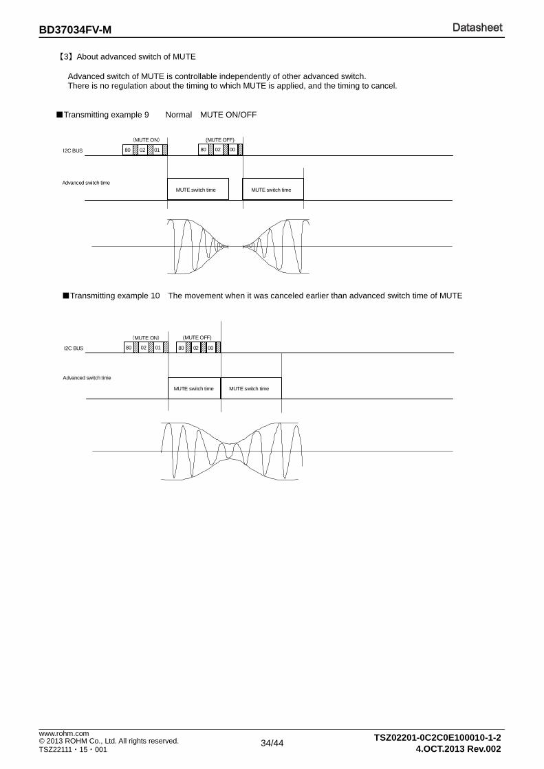
【3】About advanced switch of MUTE
Advanced switch of MUTE is controllable independently of other advanced switch. There is no regulation about the timing to which MUTE is applied, and the timing to cancel.
Transmitting example 9 Normal MUTE ON/OFF
Transmitting example 10 The movement when it was canceled earlier than advanced switch time of MUTE
80 02 01 80 02 00 I2C BUS
(MUTE ON) (MUTE OFF)
MUTE switch time Advanced switch time
MUTE switch time
80 02 01 80 02 00 I2C BUS
MUTE switch time
Advanced switch time
MUTE switch time
(MUTE ON) (MUTE OFF)
35/44
DatasheetBD37034FV-M
TSZ02201-0C2C0E100010-1-2
© 2013 ROHM Co., Ltd. All rights reserved. 4.OCT.2013 Rev.002
www.rohm.com
TSZ22111・15・001
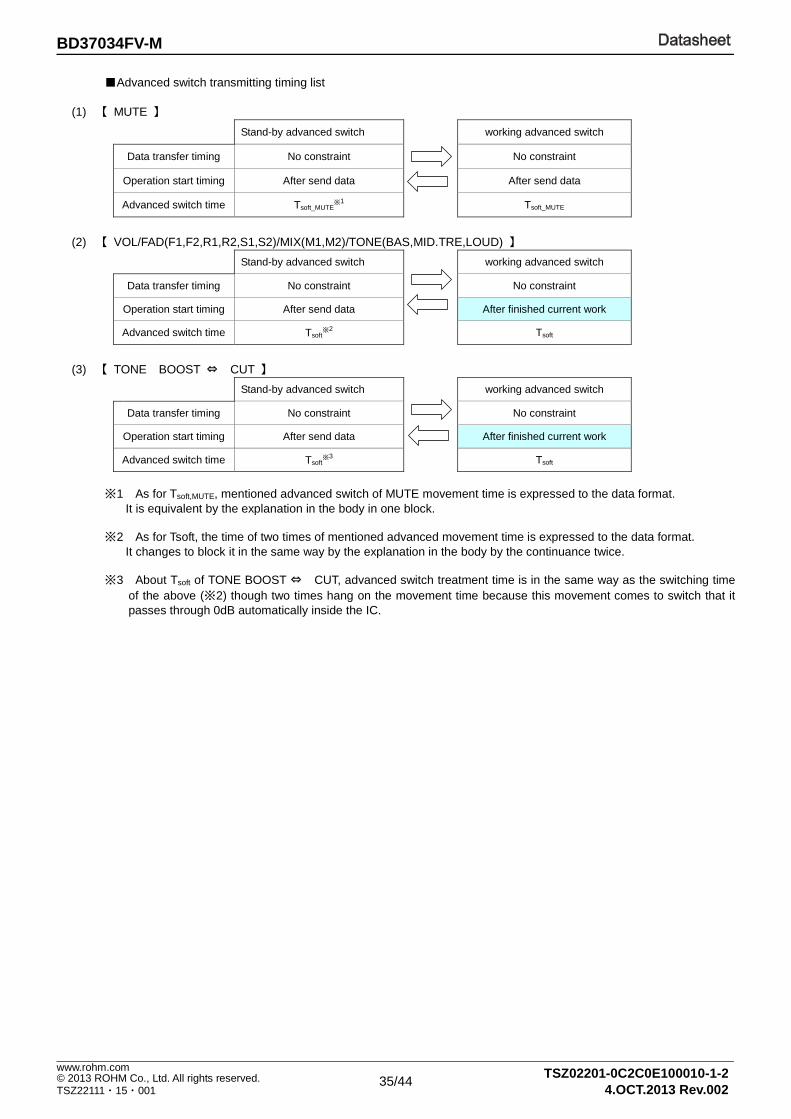
Advanced switch transmitting timing list
(1) 【 MUTE 】
Stand-by advanced switch working advanced switch
Data transfer timing No constraint No constraint
Operation start timing After send data After send data
Advanced switch time Tsoft_MUTE※
1 Tsoft_MUTE
(2) 【 VOL/FAD(F1,F2,R1,R2,S1,S2)/MIX(M1,M2)/TONE(BAS,MID.TRE,LOUD) 】
Stand-by advanced switch working advanced switch
Data transfer timing No constraint No constraint
Operation start timing After send data After finished current work
Advanced switch time Tsoft※
2 Tsoft
(3) 【 TONE BOOST ⇔ CUT 】
Stand-by advanced switch working advanced switch
Data transfer timing No constraint No constraint
Operation start timing After send data After finished current work
Advanced switch time Tsoft※
3 Tsoft
※1 As for Tsoft,MUTE, mentioned advanced switch of MUTE movement time is expressed to the data format.
It is equivalent by the explanation in the body in one block. ※2 As for Tsoft, the time of two times of mentioned advanced movement time is expressed to the data format.
It changes to block it in the same way by the explanation in the body by the continuance twice. ※3 About Tsoft of TONE BOOST ⇔ CUT, advanced switch treatment time is in the same way as the switching time
of the above (※2) though two times hang on the movement time because this movement comes to switch that it passes through 0dB automatically inside the IC.
36/44
DatasheetBD37034FV-M
TSZ02201-0C2C0E100010-1-2
© 2013 ROHM Co., Ltd. All rights reserved. 4.OCT.2013 Rev.002
www.rohm.com
TSZ22111・15・001
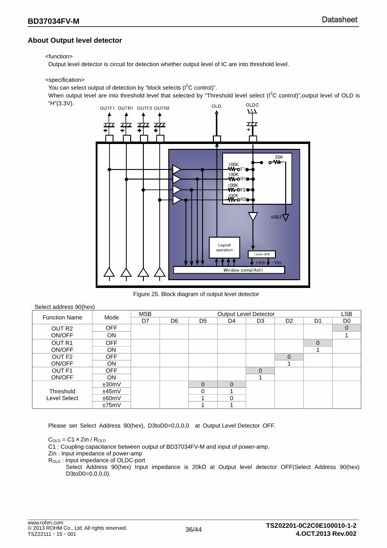
About Output level detector
<function> Output level detector is circuit for detection whether output level of IC are into threshold level.
<specification> You can select output of detection by “block selects (I2C control)”. When output level are into threshold level that selected by “Threshold level select (I2C control)”,output level of OLD is “H”(3.3V).
Select address 90(hex)
Function Name Mode MSB Output Level Detector LSB D7 D6 D5 D4 D3 D2 D1 D0
OUT R2 ON/OFF
OFF
0 ON 1
OUT R1 ON/OFF
OFF
0
ON 1 OUT F2 ON/OFF
OFF
0
ON 1 OUT F1 ON/OFF
OFF
0
ON 1
Threshold Level Select
±30mV
0 0
±45mV 0 1 ±60mV 1 0 ±75mV 1 1
Please set Select Address 90(hex), D3toD0=0,0,0,0 at Output Level Detector OFF.
COLD = C1×Zin / ROLD C1 : Coupling capacitance between output of BD37034FV-M and input of power-amp. Zin : Input impedance of power-amp ROLD : Input impedance of OLDC-port
Select Address 90(hex) Input impedance is 20kΩ at Output level detector OFF(Select Address 90(hex) D3toD0=0,0,0,0).
Figure 25. Block diagram of output level detector
37/44
DatasheetBD37034FV-M
TSZ02201-0C2C0E100010-1-2
© 2013 ROHM Co., Ltd. All rights reserved. 4.OCT.2013 Rev.002
www.rohm.com
TSZ22111・15・001
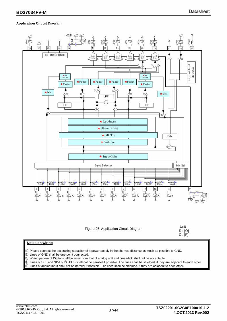
Application Circuit Diagram
Figure 26. Application Circuit Diagram
Notes on wiring ① Please connect the decoupling capacitor of a power supply in the shortest distance as much as possible to GND. ② Lines of GND shall be one-point connected. ③ Wiring pattern of Digital shall be away from that of analog unit and cross-talk shall not be acceptable. ④ Lines of SCL and SDA of I2C BUS shall not be parallel if possible. The lines shall be shielded, if they are adjacent to each other. ⑤ Lines of analog input shall not be parallel if possible. The lines shall be shielded, if they are adjacent to each other.
Unit R : [Ω] C : [F]
38/44
DatasheetBD37034FV-M
TSZ02201-0C2C0E100010-1-2
© 2013 ROHM Co., Ltd. All rights reserved. 4.OCT.2013 Rev.002
www.rohm.com
TSZ22111・15・001
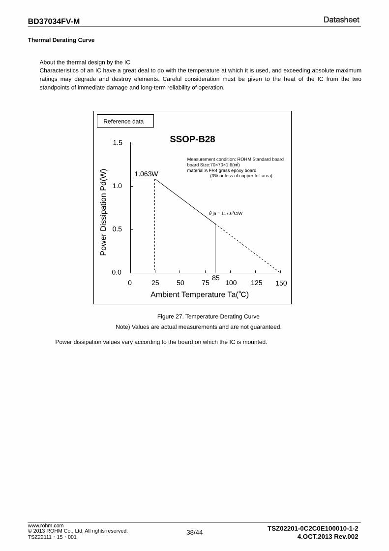
Thermal Derating Curve
About the thermal design by the IC Characteristics of an IC have a great deal to do with the temperature at which it is used, and exceeding absolute maximum ratings may degrade and destroy elements. Careful consideration must be given to the heat of the IC from the two standpoints of immediate damage and long-term reliability of operation.
Figure 27. Temperature Derating Curve
Power dissipation values vary according to the board on which the IC is mounted.
SSOP-B28 1.5
1.0
0.5
0.0
0 25 50 75 100 125 150
1.063W
θja = 117.6/W
85
Reference data
Ambient Temperature Ta()
Pow
er D
issi
patio
n P
d(W
)
Measurement condition: ROHM Standard board board Size:70×70×1.6() material:A FR4 grass epoxy board
(3% or less of copper foil area)
Note) Values are actual measurements and are not guaranteed.

39/44
DatasheetBD37034FV-M
TSZ02201-0C2C0E100010-1-2
© 2013 ROHM Co., Ltd. All rights reserved. 4.OCT.2013 Rev.002
www.rohm.com
TSZ22111・15・001
Terminal Equivalent Circuit and Description Terminal
No. Terminal
Name Terminal Voltage
Equivalent Circuit Terminal Description
1
2
3
4
5
6
A1
A2
B1
B2
C1
C2
4.15
A terminal for signal input.
The input impedance is 100kΩ(typ).
7
8
9
10
11
13
DP1
DN
DP2
EP1
EN1
EP2
4.15
A terminal for signal input.
The input impedance is 100kΩ(typ).
12 MIN
EN2 4.15
A terminal for signal input.
The input impedance is 100kΩ(typ).
15 MUTE -
A terminal for external compulsory mute. If terminal voltage is High level, the mute is off. And if the terminal voltage is Low level, the mute is on.
18
19
20
21
22
23
OUTS2
OUTS1
OUTR2
OUTR1
OUTF2
OUTF1
4.15/6.0
HiVoltage
=OFF/ON
A terminal for fader and Subwoofer output.
The figure in the pin explanation and input/output equivalent circuit is reference value, it doesn’t guarantee the value.
GND
VCCL
100KΩ
GND
VCC
100KΩ
Anti ESD
GND
VCC
100KΩ
Anti ESD
VCC
GND
VCCL
GND
1.3V
125k
5V
Anti-ESD
250k
40/44
DatasheetBD37034FV-M
TSZ02201-0C2C0E100010-1-2
© 2013 ROHM Co., Ltd. All rights reserved. 4.OCT.2013 Rev.002
www.rohm.com
TSZ22111・15・001
Terminal
No.
Terminal
Name
Terminal
Voltage Equivalent Circuit Terminal Description
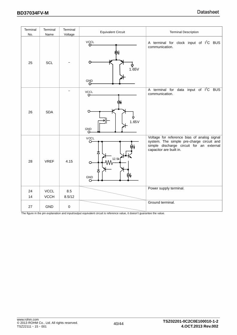
25 SCL -
A terminal for clock input of I2C BUS communication.
26 SDA
- A terminal for data input of I2C BUS communication.
28 VREF 4.15
Voltage for reference bias of analog signal system. The simple pre-charge circuit and simple discharge circuit for an external capacitor are built in.
24
14
VCCL
VCCH
8.5
8.5/12
Power supply terminal.
27 GND 0
Ground terminal.
The figure in the pin explanation and input/output equivalent circuit is reference value, it doesn’t guarantee the value.
VCCL
GND
1.65V
VCCL
GND
1.65V
VCCL
GND
12.5k

41/44
DatasheetBD37034FV-M
TSZ02201-0C2C0E100010-1-2
© 2013 ROHM Co., Ltd. All rights reserved. 4.OCT.2013 Rev.002
www.rohm.com
TSZ22111・15・001
Terminal
No.
Terminal
Name
Terminal
Voltage Equivalent Circuit Terminal Description
16
LRST -
A terminal for level meter reset. If terminal voltage is High level, the reset is on. And if the terminal voltage is Low level, the reset is off.
OLDC
4.15/
4.73
HiVoltage
=OFF/ON
A terminal for filter of output level detector.
Input impedance is 25k(OUTF/R both ON) or 50kΩ(OUTF/R either ON) at Output level detector ON, 20kΩ at Output level detector OFF.
17
LOUT
A terminal for Level meter output.
OLD
0
3.3
A terminal for output of output level detector.
The figure in the pin explanation and input/output equivalent circuit is reference value, it doesn’t guarantee the value.
VCC
GND
1.65V 100k
10k
GND
VCC
1.5k
VCCL
GND
3.3 V
1.5k
GND
VCCL
50k
OUTF2/R2
50k
42/44
DatasheetBD37034FV-M
TSZ02201-0C2C0E100010-1-2
© 2013 ROHM Co., Ltd. All rights reserved. 4.OCT.2013 Rev.002
www.rohm.com
TSZ22111・15・001
Notes for use
1.Absolute maximum rating voltage When it impressed the voltage on VCC more than the absolute maximum rating voltage, circuit currents increase rapidly, and there is absolutely a case to reach characteristic deterioration and destruction of a device. In particular in a serge examination of a set, when it is expected the impressing serge at VCC terminal (14,24pin), please do not impress the large and over the absolute maximum rating voltage (including a operating voltage + serge ingredient (around 14V))
2.About a signal input part 1)In the signal input terminal, the constant setting of input coupling capacitor C(F) be sufficient input impedance
RIN(Ω) inside IC and please decide. The first HPF characteristic of RC is composed.
2) SHORT mode is the command which makes switch SSH =ON an input selector part and input impedance RIN of all terminals, and makes resistance small. Switch SSH is OFF when not choosing a SHORT command. A constant time becomes small at the time of this command twisting to the resistance inside the capacitor connected outside and LSI. The charge time of a capacitor becomes short. Since SHORT mode turns ON the switch of SSH and makes it low impedance, please use it at the time of a non-signal.
3.About Mute terminal(15pin) when power supply is off Any voltage shall not be supplied to Mute terminal (15pin) when power-supply is off. Please insert a resistor (about 2.2kΩ) to Mute terminal in series, if voltage is supplied to mute terminal in case. (Please refer Application Circuit Diagram.)
4. About Hi-Voltage function
About Logic of Hi-Voltage function is follow as.
Hi-Voltage ON/OFF
Hi-Voltage ON ・Though the level of amplification in the output-unit is controlled with Level Shift (Select Address 01hex, D3), it
becomes a +6dB fixation under the condition of Hi-Voltage function is ON. ・Under the condition of Hi-Voltage function is OFF, 0dB/+3dB switching is possible by the setup of Level Shift. ・Under the condition of Hi-Voltage function is OFF, bias-voltage is 4.15V regardless of the setup of Level Shift. ・The use of the external MUTE on the set side is recommended because shock noise by the DC step is made when
ON/OFF switching of the Hi-Voltage function is done. ・The initial condition of Hi-Voltage function is Hi-Voltage=ON after a power supply is started)
Hivoltage ON/OFF(Select Address 01hex, D2) 0 0 1 1 - Level Shift(Select Address 01hex, D3) 0 1 0 1 - Level of amplification in the output-unit 0 3 6 6 [dB] Bias-voltage in the output-unit 4.15 4.15 6 6 [V]
2
IN)
2
IN
(2πfCR1
)(2πfCR
A(f)
+=
0
A(f)
G[dB]
F[Hz]
C[F]
RIN [Ω]
INPUT
SSH

43/44
DatasheetBD37034FV-M
TSZ02201-0C2C0E100010-1-2
© 2013 ROHM Co., Ltd. All rights reserved. 4.OCT.2013 Rev.002
www.rohm.com
TSZ22111・15・001
Ordering Information
B D 3 7 0 3 4 F V ME 2 Part Number
Package FV: SSOP-B28
Packaging and forming specification
E2: Embossed tape and reel (SSOP-B28)
Physical Dimension Tape and Reel Information
Marking Diagram(s)(TOP VIEW)
SSOP-B28(TOP VIEW)
BD37034FV
Part Number Marking
LOT Number
1PIN MARK
(Unit : mm)
SSOP-B28
0.1
0.15 ± 0.1
0.11.
15 ±
0.1
1
0.65
7.6 ± 0
.3
5.6 ± 0
.2
28
10 ± 0.2(MAX 10.35 include BURR)
0.3M
in.
14
15
0.22 ± 0.1
∗ Order quantity needs to be multiple of the minimum quantity.
<Tape and Reel information>
Embossed carrier tapeTape
Quantity
Direction of feed
The direction is the 1pin of product is at the upper left when you hold reel on the left hand and you pull out the tape on the right hand
2000pcs
E2
( )
Direction of feed
Reel1pin
44/44
DatasheetBD37034FV-M
TSZ02201-0C2C0E100010-1-2
© 2013 ROHM Co., Ltd. All rights reserved. 4.OCT.2013 Rev.002
www.rohm.com
TSZ22111・15・001
Revision history
Date Revision Changes
3.APR.2013 001 New Release
Date Revision Changes
4.OCT.2013 002 All page delete
4.OCT.2013 002 Page 2 < Sub Title> Sound Processors for Car Audios ⇒ Analog Audio Processors series change. <Feature> AEC-Q100 Qualified add. <Logo> PbFree, RoHS delete
4.OCT.2013 002 Page 3 Power Dissipation mW ⇒ W change.
4.OCT.2013 002 Page 43 Ordering Information, E2 ⇒ ME2 change.
DatasheetDatasheet
Notice - SS Rev.002© 2014 ROHM Co., Ltd. All rights reserved.
Notice Precaution on using ROHM Products
1. If you intend to use our Products in devices requiring extremely high reliability (such as medical equipment (Note 1), aircraft/spacecraft, nuclear power controllers, etc.) and whose malfunction or failure may cause loss of human life, bodily injury or serious damage to property (“Specific Applications”), please consult with the ROHM sales representative in advance. Unless otherwise agreed in writing by ROHM in advance, ROHM shall not be in any way responsible or liable for any damages, expenses or losses incurred by you or third parties arising from the use of any ROHM’s Products for Specific Applications.
(Note1) Medical Equipment Classification of the Specific Applications JAPAN USA EU CHINA
CLASSⅢ CLASSⅢ
CLASSⅡb CLASSⅢ
CLASSⅣ CLASSⅢ
2. ROHM designs and manufactures its Products subject to strict quality control system. However, semiconductor
products can fail or malfunction at a certain rate. Please be sure to implement, at your own responsibilities, adequate safety measures including but not limited to fail-safe design against the physical injury, damage to any property, which a failure or malfunction of our Products may cause. The following are examples of safety measures:
[a] Installation of protection circuits or other protective devices to improve system safety [b] Installation of redundant circuits to reduce the impact of single or multiple circuit failure
3. Our Products are not designed under any special or extraordinary environments or conditions, as exemplified below. Accordingly, ROHM shall not be in any way responsible or liable for any damages, expenses or losses arising from the use of any ROHM’s Products under any special or extraordinary environments or conditions. If you intend to use our Products under any special or extraordinary environments or conditions (as exemplified below), your independent verification and confirmation of product performance, reliability, etc, prior to use, must be necessary:
[a] Use of our Products in any types of liquid, including water, oils, chemicals, and organic solvents [b] Use of our Products outdoors or in places where the Products are exposed to direct sunlight or dust [c] Use of our Products in places where the Products are exposed to sea wind or corrosive gases, including Cl2,
H2S, NH3, SO2, and NO2
[d] Use of our Products in places where the Products are exposed to static electricity or electromagnetic waves [e] Use of our Products in proximity to heat-producing components, plastic cords, or other flammable items [f] Sealing or coating our Products with resin or other coating materials [g] Use of our Products without cleaning residue of flux (even if you use no-clean type fluxes, cleaning residue of
flux is recommended); or Washing our Products by using water or water-soluble cleaning agents for cleaning residue after soldering
[h] Use of the Products in places subject to dew condensation
4. The Products are not subject to radiation-proof design. 5. Please verify and confirm characteristics of the final or mounted products in using the Products. 6. In particular, if a transient load (a large amount of load applied in a short period of time, such as pulse. is applied,
confirmation of performance characteristics after on-board mounting is strongly recommended. Avoid applying power exceeding normal rated power; exceeding the power rating under steady-state loading condition may negatively affect product performance and reliability.
7. De-rate Power Dissipation (Pd) depending on Ambient temperature (Ta). When used in sealed area, confirm the actual
ambient temperature. 8. Confirm that operation temperature is within the specified range described in the product specification. 9. ROHM shall not be in any way responsible or liable for failure induced under deviant condition from what is defined in
this document.
Precaution for Mounting / Circuit board design 1. When a highly active halogenous (chlorine, bromine, etc.) flux is used, the residue of flux may negatively affect product
performance and reliability. 2. In principle, the reflow soldering method must be used; if flow soldering method is preferred, please consult with the
ROHM representative in advance. For details, please refer to ROHM Mounting specification

DatasheetDatasheet
Notice - SS Rev.002© 2014 ROHM Co., Ltd. All rights reserved.
Precautions Regarding Application Examples and External Circuits 1. If change is made to the constant of an external circuit, please allow a sufficient margin considering variations of the
characteristics of the Products and external components, including transient characteristics, as well as static characteristics.
2. You agree that application notes, reference designs, and associated data and information contained in this document
are presented only as guidance for Products use. Therefore, in case you use such information, you are solely responsible for it and you must exercise your own independent verification and judgment in the use of such information contained in this document. ROHM shall not be in any way responsible or liable for any damages, expenses or losses incurred by you or third parties arising from the use of such information.
Precaution for Electrostatic
This Product is electrostatic sensitive product, which may be damaged due to electrostatic discharge. Please take proper caution in your manufacturing process and storage so that voltage exceeding the Products maximum rating will not be applied to Products. Please take special care under dry condition (e.g. Grounding of human body / equipment / solder iron, isolation from charged objects, setting of Ionizer, friction prevention and temperature / humidity control).
Precaution for Storage / Transportation 1. Product performance and soldered connections may deteriorate if the Products are stored in the places where:
[a] the Products are exposed to sea winds or corrosive gases, including Cl2, H2S, NH3, SO2, and NO2 [b] the temperature or humidity exceeds those recommended by ROHM [c] the Products are exposed to direct sunshine or condensation [d] the Products are exposed to high Electrostatic
2. Even under ROHM recommended storage condition, solderability of products out of recommended storage time period may be degraded. It is strongly recommended to confirm solderability before using Products of which storage time is exceeding the recommended storage time period.
3. Store / transport cartons in the correct direction, which is indicated on a carton with a symbol. Otherwise bent leads
may occur due to excessive stress applied when dropping of a carton. 4. Use Products within the specified time after opening a humidity barrier bag. Baking is required before using Products of
which storage time is exceeding the recommended storage time period.
Precaution for Product Label QR code printed on ROHM Products label is for ROHM’s internal use only.
Precaution for Disposition When disposing Products please dispose them properly using an authorized industry waste company.
Precaution for Foreign Exchange and Foreign Trade act Since our Products might fall under controlled goods prescribed by the applicable foreign exchange and foreign trade act, please consult with ROHM representative in case of export.
Precaution Regarding Intellectual Property Rights 1. All information and data including but not limited to application example contained in this document is for reference
only. ROHM does not warrant that foregoing information or data will not infringe any intellectual property rights or any other rights of any third party regarding such information or data. ROHM shall not be in any way responsible or liable for infringement of any intellectual property rights or other damages arising from use of such information or data.:
2. No license, expressly or implied, is granted hereby under any intellectual property rights or other rights of ROHM or any
third parties with respect to the information contained in this document.
Other Precaution 1. This document may not be reprinted or reproduced, in whole or in part, without prior written consent of ROHM. 2. The Products may not be disassembled, converted, modified, reproduced or otherwise changed without prior written
consent of ROHM. 3. In no event shall you use in any way whatsoever the Products and the related technical information contained in the
Products or this document for any military purposes, including but not limited to, the development of mass-destruction weapons.
4. The proper names of companies or products described in this document are trademarks or registered trademarks of
ROHM, its affiliated companies or third parties.

DatasheetDatasheet
Notice – WE Rev.001© 2014 ROHM Co., Ltd. All rights reserved.
General Precaution 1. Before you use our Pro ducts, you are requested to care fully read this document and fully understand its contents.
ROHM shall n ot be in an y way responsible or liabl e for fa ilure, malfunction or acci dent arising from the use of a ny ROHM’s Products against warning, caution or note contained in this document.
2. All information contained in this docume nt is current as of the issuing date and subj ect to change without any prior
notice. Before purchasing or using ROHM’s Products, please confirm the la test information with a ROHM sale s representative.
3. The information contained in this doc ument is provi ded on an “as is” basis and ROHM does not warrant that all
information contained in this document is accurate an d/or error-free. ROHM shall not be in an y way responsible or liable for any damages, expenses or losses incurred by you or third parties resulting from inaccuracy or errors of or concerning such information.