generation and detection of spin currents in semiconductor...
TRANSCRIPT

Generation and Detection of Spin Currents in Semiconductor Nanostructures with StrongSpin-Orbit Interaction
Fabrizio Nichele,1,* Szymon Hennel,1 Patrick Pietsch,1 Werner Wegscheider,1 Peter Stano,2,3 Philippe Jacquod,4
Thomas Ihn,1 and Klaus Ensslin11Solid State Physics Laboratory, ETH Zürich, 8093 Zürich, Switzerland
2RIKEN Center for Emergent Matter Science, 2-1 Hirosawa, Wako, Saitama 351-0198, Japan3Institute of Physics, Slovak Academy of Sciences, Dubravska cesta 9, 84511 Bratislava, Slovakia
4HES-SO, Haute Ecole d’Ingénierie, 1950 Sion, Switzerland(Received 14 September 2014; revised manuscript received 28 April 2015; published 18 May 2015)
Storing, transmitting, and manipulating information using the electron spin resides at the heart ofspintronics. Fundamental for future spintronics applications is the ability to control spin currents in solidstate systems. Among the different platforms proposed so far, semiconductors with strong spin-orbitinteraction are especially attractive as they promise fast and scalable spin control with all-electricalprotocols. Here we demonstrate both the generation and measurement of pure spin currents insemiconductor nanostructures. Generation is purely electrical and mediated by the spin dynamics inmaterials with a strong spin-orbit field. Measurement is accomplished using a spin-to-charge conversiontechnique, based on the magnetic field symmetry of easily measurable electrical quantities. Calibrating thespin-to-charge conversion via the conductance of a quantum point contact, we quantitatively measure themesoscopic spin Hall effect in a multiterminal GaAs dot. We report spin currents of 174 pA, correspondingto a spin Hall angle of 34%.
DOI: 10.1103/PhysRevLett.114.206601 PACS numbers: 72.25.Dc, 72.25.Hg, 73.23.−b, 75.76.+j
The generation and detection of spin currents in nano-structures is the central challenge of semiconductor spin-tronics. On the one hand, spin injection cannot be easilyachieved by coupling semiconductors to ferromagnets [1]because of the lack of control over material interfaces [2].On the other hand, magnetoelectric alternatives exploitingthe celebrated spin Hall effect (SHE) [3,4], have deliveredonly qualitative measurement protocols in transport experi-ments [5]. Alternatively to all-electrical setups, spin polar-izing the current through a quantum point contact (QPC)with a magnetic field allows a quantitative control over spincurrent generation and detection at the nanoscale [6–8].The latter approach requires, however, such high magneticfields (6–8 T), that the desired magnetoelectric effects areeither suppressed or totally altered.This Letter reports two major advances of nanoscale
semiconductor spintronics.Namely,wedevelopnovel exper-imental methods to electrically generate and quantitativelymeasure spin currents in a two-dimensional semiconductornanostructure.It is predicted that charge currents flowing through spin-
orbit interaction (SOI)-coupled nanostructures are generi-cally accompanied by spin currents, if the spin-orbit timeis shorter than the electron dwell time [9–12]. This spincurrent generation mechanism is purely electrical and basedon the mesoscopic SHE (MSHE) [9,10], where the elec-tronic orbital dynamics in chaotic nanostructures cooper-ates with the SOI to make transport spin dependent. Wewillconsider an open three-terminal quantum dot as represented
in Fig. 1(a), where each lead i is a QPC carrying Ni spindegenerate modes. Running a charge current I betweenterminals 1 and 2, a spin current in all terminals, including3, is expected due to the MSHE.For a weak SOI, the spin currents’ amplitude fluctuates
from sample to sample with zero average. For cavities witha strong SOI, geometric correlations between the spin and
I =03
B=0
I <03
B>0
I >03
B<0
B<0
B=0
B>0
EnergyE0
1
0.5
0I
I
(s)I3
1
2
3B
Spin 1Spin 2
(a) (b)
(c)
(Spi
n 1)
T33
EZ
E =gµ BZ B
FIG. 1 (color online). (a) Schematic of the system used togenerate spin currents. Charge currents are depicted as blacklines, spin currents are depicted as red and blue lines. (b) Energydependent, spin sensitive, transmission probability of QPC3. Atzero field the transmission is tuned to 1=2. A positive (negative)field suppresses (enhances) the transmission probability of onespin eigenstate. (c) Representation of spin and charge currents inQPC3 as a function of magnetic field. The net charge current inQPC3 varies with the magnetic field.
PRL 114, 206601 (2015) P HY S I CA L R EV I EW LE T T ER Sweek ending22 MAY 2015
0031-9007=15=114(20)=206601(5) 206601-1 © 2015 American Physical Society
the orbital electronic dynamics lead to spin currents withlarge, predictable nonzero average values [13]. In the lattercase, the spin currents’ amplitude is determined by thenanostructure geometry and the SOI strength. This par-ticular mechanism renders spin currents robust againstdecoherence and allows us to differentiate them frommesoscopic fluctuations. This is essential for spintronicsapplications, where spin currents must be reproducibleregardless of the microscopic details of the sample.To detect and measure the spin currents described above,
we employ the scheme of Ref. [14], based on the magneticfield parity of the voltage behind a QPC. With referenceto Fig. 1(a), we are interested in the spin current IðSÞ3 emittedfrom QPC3. The energy dependent transmission probability
of QPC3, TðsÞ33 , is shown in Fig. 1(b). At zero field, QPC3 is
tuned to a conductance of e2=h by a suitable gate voltage,corresponding to a spin-independent transmission probabil-ity of one half.Aweak in-planemagnetic fieldBmodifies theelectrons’ kinetic energy via Zeeman coupling, selectivelyincreasing or decreasing the transmission probabilityaccording to the spin eigenstate and magnetic field sign.
For simplicity, we assume IðSÞ3 to be a pure spin current atB ¼ 0, arising as two counterpropagating and inversely spin-polarized charge currents of equal magnitude, as schemati-cally shown in Fig. 1(c), where arrows indicate currentamplitude and colors spin polarization. A magnetic fieldaffects the QPC spin dependent transmission probability,enhancing one of the two charge currents and suppressing theother. The result is the flow of a net charge current I3 in theQPC. The sign of I3 reverses by reversing the magnetic fieldsign. Note that the net spin current remains constant in thethree situations depicted in Fig. 1(c).By operating QPC3 as a floating probe, the charge
current I3 is constantly fixed to zero. In this case, the
presence of a spin current IðSÞ3 in the QPC reflects itself inan antisymmetric component of the voltage behind it:V3ðBÞ ≠ V3ð−BÞ. Remarkably, theory predicts that thezero-field derivative of the measured voltage, ∂BV3, is
proportional to the spin current IðSÞ3 polarized along theapplied magnetic field. The proportionality coefficient
between the spin-to-charge signal ∂BV3 and IðSÞ3 is givenby the QPC g factor and its energy sensitivity ℏω measuredat N3 ¼ 0.5 [14]:
IðSÞ3 ¼ e2
h2ℏωπgμB
∂BV3: ð1Þ
More generally, for N3 ≤ 1 the presence of the spincurrent still reflects itself in a finite spin-to-charge signalwhose amplitude is directly proportional to the detectornormalized transconductance: ∂BV3 ∝ ∂VG3=G3. ForN3 ¼ 0.5 it results in ∂VG3=G3 ¼ −π=ℏω. Details aboutthe derivation of this proportionality and Eq. (1) arereported in the Supplemental Material [15]. Equation (1)
not only allows us to detect the presence of a spin currentflowing in QPC3, but also to quantitatively measure andexpress it in units of ampere, giving the difference incurrents carried by electrons with opposite polarization.Given the large SOI of our system, the measurementprocess requires only weak magnetic fields that do notaffect the generated spin currents. We note that ourapproach is restricted to the linear response regime, andto terminal 3 being a weak probe, i.e., N3 ≤ 1 ≪ N1; N2.The measurement protocol described here is independent ofthe spin current generation mechanism. In particular, thedetection method can be used to measure spin currents ofother origin.Motivated by the theory above, we study a three-terminal
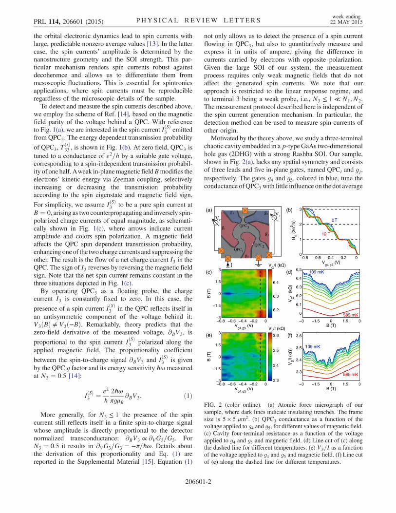
chaotic cavity embedded in ap-typeGaAs two-dimensionalhole gas (2DHG) with a strong Rashba SOI. Our sample,shown in Fig. 2(a), lacks any spatial symmetry and consistsof three leads and five in-plane gates, named QPCi and gj,respectively. The gates g4 and g5, colored in blue, tune theconductance ofQPC3 with little influence on the dot average
Vg4,g5
(V)
B (
T)
−0.8 −0.6 −0.4 −0.2 0−3
−1.5
0
1.5
3
6.2
6.3
6.4
−3 −1.5 0 1.5 3
3.3
3.4
3.5
3.6
B (T)
V3/I
(k)
−3 −1.5 0 1.5 3
6
6.1
6.2
6.3
6.4
6.5
B (T)
VC/I
(k)
Vg4,g5
(V)
B (
T)
−0.8 −0.6 −0.4 −0.2 0−3
−1.5
0
1.5
3
3.3
3.4
3.5
3.6
−0.8 −0.6 −0.4 −0.2 00
1
2
3
Vg4,g5
(V)
G3 (
2e2 /h
)
(a)
(c)
(b)
(d)
(f)(e)
12 T
0 T
109 mK
585 mK
109 mK
585 mK
V3/I (k )
VC/I (k )
g1
g2
g3
g4g5
QPC1
QPC2
I
V3
QPC3
VC
FIG. 2 (color online). (a) Atomic force micrograph of oursample, where dark lines indicate insulating trenches. The framesize is 5 × 5 μm2. (b) QPC3 conductance as a function of thevoltage applied to g4 and g5, for different values of magnetic field.(c) Cavity four-terminal resistance as a function of the voltageapplied to g4 and g5 and magnetic field. (d) Line cut of (c) alongthe dashed line for different temperatures. (e) V3=I as a functionof the voltage applied to g4 and g5 and magnetic field. (f) Line cutof (e) along the dashed line for different temperatures.
PRL 114, 206601 (2015) P HY S I CA L R EV I EW LE T T ER Sweek ending22 MAY 2015
206601-2
conductance. The gates g1, g2, and g3, depicted in red, tunethe conductance of QPC1 and QPC2, and also affect thedot shape. The lateral extent of the cavity is about 2 μm, thehole mean free path le ¼ 4.8 μm, and the spin-orbit lengthlSO ¼ 36 nm [15]. Spin rotational symmetry is then com-pletely broken and, with such a strong SOI, our cavity isin the so-called spin chaos regime [13]. Unless differentlystated, a charge current I flows from terminal 1 to terminal 2,while terminal 3 is connected to a high impedance voltageamplifier and is used to measure spin currents.To measure the spin current in terminal 3, we first extract
the detector electric and magnetic sensitivity via a standardQPC characterization. Figure 2(b) shows the detectorconductance G3 as a function of side gate voltage fordifferent values of a magnetic field aligned with the QPC3
axis. The three well-developed plateaus visible at zero fieldsplit at finite field. The zero field slope and the finite fieldsplitting give, respectively, ∂VG3 and the g factor [15].After the detector calibration, QPC3 is operated as a
voltage probe. The spin current measurement is performedrunning an ac current (I ¼ 4 nA unless stated otherwise)between terminals 1 and 2, and measuring the magneticdependence of the voltages VC and V3 as defined inFig. 2(a). The magnetic field is applied in-plane, tominimize its orbital effects, and aligned with the detectoraxis (unless stated otherwise). The finite zero field deriva-tive ∂BV3, and its correlation with ∂VG3=G3, indicates the
presence of the spin current IðSÞ3 .Figures 2(c) and 2(e) show the resistances RC ¼ VC=I
and V3=I as a function of B and the voltage applied to g4and g5. Panels (d) and (f) show line cuts along the dashedlines of Figs. 2(c) and 2(e), respectively, for differenttemperatures. These line cuts are taken for N3 ¼ 0.5. Ontop of a smooth background, higher frequency conductancefluctuations (CFs) appear at low temperatures. The cavityresistance RC is symmetric upon magnetic field reversalboth in the slowly varying background and in the CFs, asexpected from a two-terminal measurement in the linearregime [21]. V3 is, on the contrary, strongly asymmetric.We first address the slowly varying background of V3ðBÞ.We will discuss the nature of the CFs below.Large CFs do not allow us to measure meaningful
voltage asymmetries at small magnetic fields. We thereforeaverage them out by a linear regression of V3ðBÞ in amagnetic field range between −1 T and 1 T. The chosenrange is an optimal compromise between not sufficient CFsaveraging at small fields and unwanted changes of the spincurrent at large fields. This interval includes at least sixCFs, and we carefully checked that the averaged voltageasymmetry only weakly depends on the precise magneticfield range used for the analysis.The detector voltage asymmetry extracted in this way is
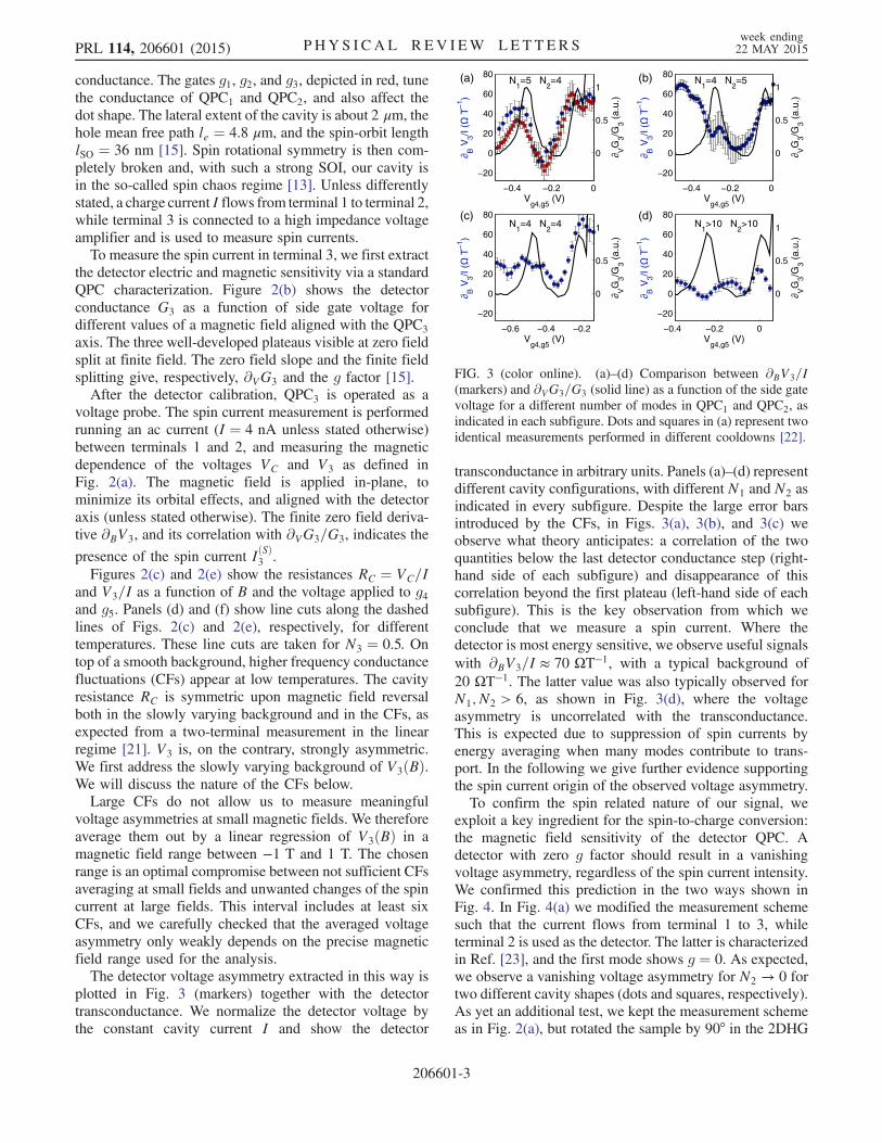
plotted in Fig. 3 (markers) together with the detectortransconductance. We normalize the detector voltage bythe constant cavity current I and show the detector
transconductance in arbitrary units. Panels (a)–(d) representdifferent cavity configurations, with different N1 and N2 asindicated in every subfigure. Despite the large error barsintroduced by the CFs, in Figs. 3(a), 3(b), and 3(c) weobserve what theory anticipates: a correlation of the twoquantities below the last detector conductance step (right-hand side of each subfigure) and disappearance of thiscorrelation beyond the first plateau (left-hand side of eachsubfigure). This is the key observation from which weconclude that we measure a spin current. Where thedetector is most energy sensitive, we observe useful signalswith ∂BV3=I ≈ 70 ΩT−1, with a typical background of20 ΩT−1. The latter value was also typically observed forN1; N2 > 6, as shown in Fig. 3(d), where the voltageasymmetry is uncorrelated with the transconductance.This is expected due to suppression of spin currents byenergy averaging when many modes contribute to trans-port. In the following we give further evidence supportingthe spin current origin of the observed voltage asymmetry.To confirm the spin related nature of our signal, we
exploit a key ingredient for the spin-to-charge conversion:the magnetic field sensitivity of the detector QPC. Adetector with zero g factor should result in a vanishingvoltage asymmetry, regardless of the spin current intensity.We confirmed this prediction in the two ways shown inFig. 4. In Fig. 4(a) we modified the measurement schemesuch that the current flows from terminal 1 to 3, whileterminal 2 is used as the detector. The latter is characterizedin Ref. [23], and the first mode shows g ¼ 0. As expected,we observe a vanishing voltage asymmetry for N2 → 0 fortwo different cavity shapes (dots and squares, respectively).As yet an additional test, we kept the measurement schemeas in Fig. 2(a), but rotated the sample by 90° in the 2DHG
−0.4 −0.2 0
−20
0
20
40
60
80
Vg4,g5
(V)
B V
3−
1 )
0
0.5
1
VG
3/G3 (
a.u.
)
−0.6 −0.4 −0.2
−20
0
20
40
60
80
Vg4,g5
(V)
B V
3−
1 )
0
0.5
1
VG
3/G3 (
a.u.
)
−0.4 −0.2 0
−20
0
20
40
60
80
Vg4,g5
(V)
B V
3−
1 )
0
0.5
1
VG
3/G3 (
a.u.
)
−0.4 −0.2 0
−20
0
20
40
60
80
Vg4,g5
(V)
B V
3
/I(
T/I
(T
/I(
T/I
(T
−1 )
0
0.5
1
VG
3/G3 (
a.u.
)
(a)
(c)
(b)
(d)N
1=4 N
2=4 N
1>10 N
2>10
N1=5 N
2=4 N
1=4 N
2=5
FIG. 3 (color online). (a)–(d) Comparison between ∂BV3=I(markers) and ∂VG3=G3 (solid line) as a function of the side gatevoltage for a different number of modes in QPC1 and QPC2, asindicated in each subfigure. Dots and squares in (a) represent twoidentical measurements performed in different cooldowns [22].
PRL 114, 206601 (2015) P HY S I CA L R EV I EW LE T T ER Sweek ending22 MAY 2015
206601-3
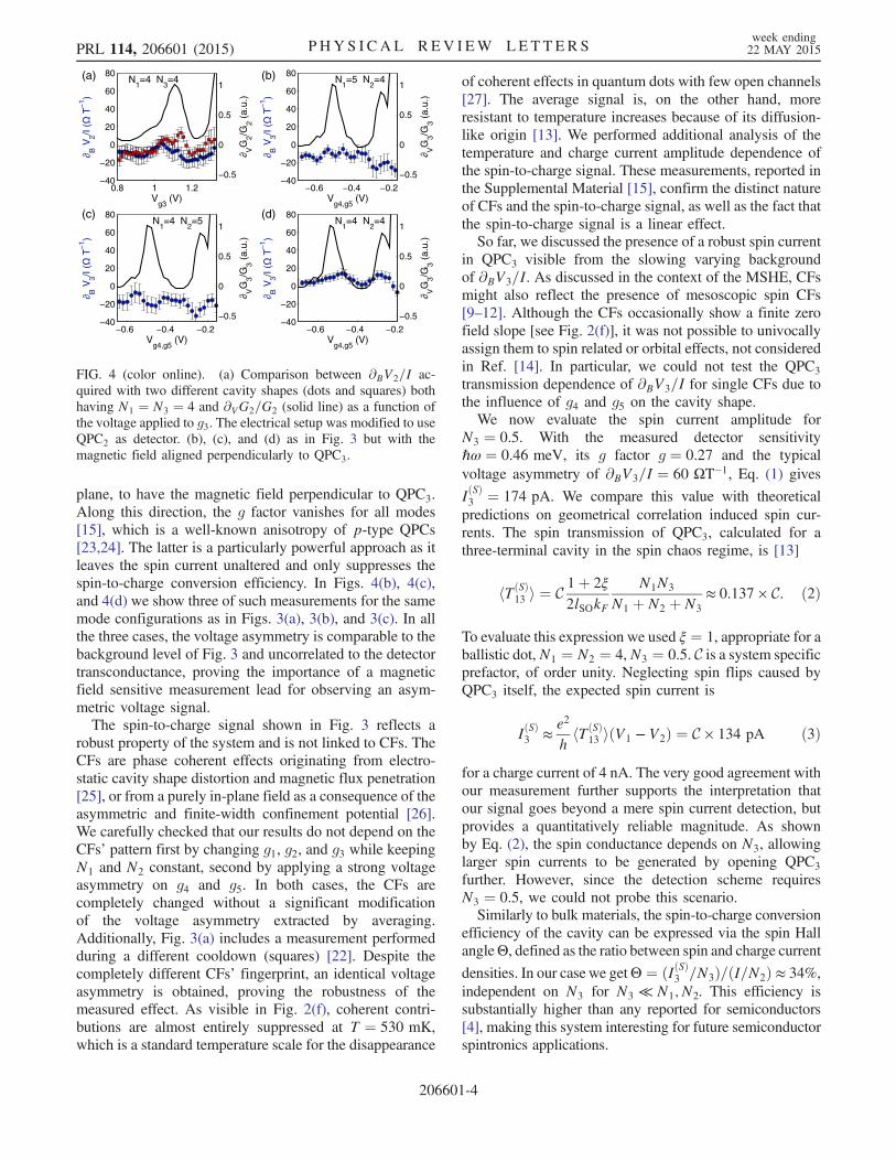
plane, to have the magnetic field perpendicular to QPC3.Along this direction, the g factor vanishes for all modes[15], which is a well-known anisotropy of p-type QPCs[23,24]. The latter is a particularly powerful approach as itleaves the spin current unaltered and only suppresses thespin-to-charge conversion efficiency. In Figs. 4(b), 4(c),and 4(d) we show three of such measurements for the samemode configurations as in Figs. 3(a), 3(b), and 3(c). In allthe three cases, the voltage asymmetry is comparable to thebackground level of Fig. 3 and uncorrelated to the detectortransconductance, proving the importance of a magneticfield sensitive measurement lead for observing an asym-metric voltage signal.The spin-to-charge signal shown in Fig. 3 reflects a
robust property of the system and is not linked to CFs. TheCFs are phase coherent effects originating from electro-static cavity shape distortion and magnetic flux penetration[25], or from a purely in-plane field as a consequence of theasymmetric and finite-width confinement potential [26].We carefully checked that our results do not depend on theCFs’ pattern first by changing g1, g2, and g3 while keepingN1 and N2 constant, second by applying a strong voltageasymmetry on g4 and g5. In both cases, the CFs arecompletely changed without a significant modificationof the voltage asymmetry extracted by averaging.Additionally, Fig. 3(a) includes a measurement performedduring a different cooldown (squares) [22]. Despite thecompletely different CFs’ fingerprint, an identical voltageasymmetry is obtained, proving the robustness of themeasured effect. As visible in Fig. 2(f), coherent contri-butions are almost entirely suppressed at T ¼ 530 mK,which is a standard temperature scale for the disappearance
of coherent effects in quantum dots with few open channels[27]. The average signal is, on the other hand, moreresistant to temperature increases because of its diffusion-like origin [13]. We performed additional analysis of thetemperature and charge current amplitude dependence ofthe spin-to-charge signal. These measurements, reported inthe Supplemental Material [15], confirm the distinct natureof CFs and the spin-to-charge signal, as well as the fact thatthe spin-to-charge signal is a linear effect.So far, we discussed the presence of a robust spin current
in QPC3 visible from the slowing varying backgroundof ∂BV3=I. As discussed in the context of the MSHE, CFsmight also reflect the presence of mesoscopic spin CFs[9–12]. Although the CFs occasionally show a finite zerofield slope [see Fig. 2(f)], it was not possible to univocallyassign them to spin related or orbital effects, not consideredin Ref. [14]. In particular, we could not test the QPC3
transmission dependence of ∂BV3=I for single CFs due tothe influence of g4 and g5 on the cavity shape.We now evaluate the spin current amplitude for
N3 ¼ 0.5. With the measured detector sensitivityℏω ¼ 0.46 meV, its g factor g ¼ 0.27 and the typicalvoltage asymmetry of ∂BV3=I ¼ 60 ΩT−1, Eq. (1) givesIðSÞ3 ¼ 174 pA. We compare this value with theoreticalpredictions on geometrical correlation induced spin cur-rents. The spin transmission of QPC3, calculated for athree-terminal cavity in the spin chaos regime, is [13]
hTðSÞ13 i ¼ C
1þ 2ξ
2lSOkF
N1N3
N1 þ N2 þ N3
≈ 0.137 × C: ð2Þ
To evaluate this expression we used ξ ¼ 1, appropriate for aballistic dot,N1 ¼ N2 ¼ 4,N3 ¼ 0.5. C is a system specificprefactor, of order unity. Neglecting spin flips caused byQPC3 itself, the expected spin current is
IðSÞ3 ≈e2
hhTðSÞ
13 iðV1 − V2Þ ¼ C × 134 pA ð3Þ
for a charge current of 4 nA. The very good agreement withour measurement further supports the interpretation thatour signal goes beyond a mere spin current detection, butprovides a quantitatively reliable magnitude. As shownby Eq. (2), the spin conductance depends on N3, allowinglarger spin currents to be generated by opening QPC3
further. However, since the detection scheme requiresN3 ¼ 0.5, we could not probe this scenario.Similarly to bulk materials, the spin-to-charge conversion
efficiency of the cavity can be expressed via the spin HallangleΘ, defined as the ratio between spin and charge currentdensities. In our case we getΘ ¼ ðIðSÞ3 =N3Þ=ðI=N2Þ ≈ 34%,independent on N3 for N3 ≪ N1; N2. This efficiency issubstantially higher than any reported for semiconductors[4], making this system interesting for future semiconductorspintronics applications.
0.8 1 1.2−40
−20
0
20
40
60
80
Vg3
(V)
B V
2−
1 )
−0.5
0
0.5
1
VG
2/G2 (
a.u.
)
−0.6 −0.4 −0.2−40
−20
0
20
40
60
80
Vg4,g5
(V)
B V
3−
1 )
−0.5
0
0.5
1
VG
3/G3 (
a.u.
)
−0.6 −0.4 −0.2−40
−20
0
20
40
60
80
Vg4,g5
(V)
B V
3−
1 )
−0.5
0
0.5
1
VG
3/G3 (
a.u.
)
−0.6 −0.4 −0.2−40
−20
0
20
40
60
80
Vg4,g5
(V)
B V
3
/I (
T
/I (
T
/I (
T
/I (
T−
1 )
−0.5
0
0.5
1
VG
3/G3 (
a.u.
)
(a)
(c)
(b)
(d)N
1=4 N
2=5 N
1=4 N
2=4
N1=4 N
3=4 N
1=5 N
2=4
FIG. 4 (color online). (a) Comparison between ∂BV2=I ac-quired with two different cavity shapes (dots and squares) bothhaving N1 ¼ N3 ¼ 4 and ∂VG2=G2 (solid line) as a function ofthe voltage applied to g3. The electrical setup was modified to useQPC2 as detector. (b), (c), and (d) as in Fig. 3 but with themagnetic field aligned perpendicularly to QPC3.
PRL 114, 206601 (2015) P HY S I CA L R EV I EW LE T T ER Sweek ending22 MAY 2015
206601-4

We acknowledge Christian Gerl for growing the waferstructure. The authors wish to thank the Swiss NationalScience Foundation via NCCR QSIT “Quantum Scienceand Technology” for financial support.
*Present Address: Center for Quantum Devices, Niels BohrInstitute, University of Copenhagen, 2100 Copenhagen,Denmark. [email protected]; http://www.nanophys.ethz.ch
[1] G. Schmidt, D. Ferrand, L. W. Molenkamp, A. T. Filip, andB. J. van Wees, Phys. Rev. B 62, R4790 (2000).
[2] S. Sharma, A. Spiesser, S. P. Dash, S. Iba, S. Watanabe, B. J.van Wees, H. Saito, S. Yuasa, and R. Jansen, Phys. Rev. B89, 075301 (2014).
[3] M. I. D’yakonov and V. I. Perel’, JETP Lett. 13, 467 (1971).[4] T. Jungwirth, J. Wunderlich, and K. Olejnik, Nat. Mater. 11,
382 (2012).[5] C. Brüne, A. Roth, E. G. Novik, M. Konig, H. Buhmann,
E. M. Hankiewicz, W. Hanke, J. Sinova, and L. W.Molenkamp, Nat. Phys. 6, 448 (2010).
[6] R. M. Potok, J. A. Folk, C. M. Marcus, and V. Umansky,Phys. Rev. Lett. 89, 266602 (2002).
[7] S. K. Watson, R. M. Potok, C. M. Marcus, and V. Umansky,Phys. Rev. Lett. 91, 258301 (2003).
[8] S. M. Frolov, A. Venkatesan, W. Yu, J. A. Folk, andW. Wegscheider, Phys. Rev. Lett. 102, 116802 (2009).
[9] W. Ren, Z. Qiao, J. Wang, Q. Sun, and H. Guo, Phys. Rev.Lett. 97, 066603 (2006).
[10] J. H. Bardarson, I. Adagideli, and P. Jacquod, Phys. Rev.Lett. 98, 196601 (2007).
[11] Y. V. Nazarov, New J. Phys. 9, 352 (2007).[12] J. J. Krich and B. I. Halperin, Phys. Rev. B 78, 035338
(2008).[13] I. Adagideli, P. Jacquod, M. Scheid, M. Duckheim, D. Loss,
and K. Richter, Phys. Rev. Lett. 105, 246807 (2010).[14] P. Stano and P. Jacquod, Phys. Rev. Lett. 106, 206602
(2011).
[15] See Supplemental Material at http://link.aps.org/supplemental/10.1103/PhysRevLett.114.206601 formaterial and methods, temperature and current dependencestudies, and a theoretical treatment of the spin-to-chargeconversion effect, which includes Refs. [16–20].
[16] F. Nichele, A. N. Pal, R. Winkler, C. Gerl, W. Wegscheider,T. Ihn, and K. Ensslin, Phys. Rev. B 89, 081306(2014).
[17] R. Winkler, Spin-Orbit Coupling Effects in Two-Dimensional Electron and Hole Systems, SpringerTracts in Modern Physics Vol. 191 (Springer-Verlag, Berlin,2003).
[18] M. Büttiker, Phys. Rev. B 41, 7906 (1990).[19] C. Rössler, S. Baer, E. de Wiljes, P.-L. Ardelt, T. Ihn, K.
Ensslin, C. Reichl, and W. Wegscheider, New J. Phys. 13,113006 (2011).
[20] P. Stano, J. Fabian, and P. Jacquod, Phys. Rev. B 85,241301(R) (2012).
[21] H. B. G. Casimir, Rev. Mod. Phys. 17, 343 (1945).[22] For a direct comparison, we horizontally shifted the red
curve to account for the different pinch-off voltage of QPC3
in this cooldown.[23] F. Nichele, S. Chesi, S. Hennel, A. Wittmann, C. Gerl, W.
Wegscheider, D. Loss, T. Ihn, and K. Ensslin, Phys. Rev.Lett. 113, 046801 (2014).
[24] A. Srinivasan, L. A. Yeoh, O. Klochan, T. P. Martin, J. C. H.Chen, A. P. Micolich, A. R. Hamilton, D. Reuter, and A. D.Wieck, Nano Lett. 13, 148 (2013).
[25] C. Beenakker and H. van Houten, in SemiconductorHeterostructures and Nanostructures, edited by H.Ehrenreich and D. Turnbull (Academic Press, New York,1991), Vol. 44, pp. 1–228.
[26] D. M. Zumbühl, J. B. Miller, C. M. Marcus, V. I. Fal’ko,T. Jungwirth, and J. S. Harris, Phys. Rev. B 69, 121305(2004).
[27] A. G. Huibers, J. A. Folk, S. R. Patel, C. M. Marcus,C. I. Duruöz, and J. S. Harris, Phys. Rev. Lett. 83, 5090(1999).
PRL 114, 206601 (2015) P HY S I CA L R EV I EW LE T T ER Sweek ending22 MAY 2015
206601-5

Generation and detection of spin currents in semiconductor
nanostructures with strong spin-orbit interaction
Fabrizio Nichele,1, ∗ Szymon Hennel,1 Patrick Pietsch,1 Werner Wegscheider,1
Peter Stano,2, 3 Philippe Jacquod,4 Thomas Ihn,1 and Klaus Ensslin1
1Solid State Physics Laboratory, ETH Zurich, 8093 Zurich, Switzerland
2RIKEN Center for Emergent Matter Science, Wako, Saitama, Japan
3Institute of Physics, Slovak Academy of Sciences,
Dubravska cesta 9, 84511 Bratislava, Slovakia
4HES-SO, Haute Ecole d’Ingenierie, 1950 Sion, Switzerland
(Dated: April 28, 2015)
Abstract
In this Supplemental Material section we provide additional information on the wafer structure
used for the experiment and on the techniques adopted to measure the sample and characterize
the detector QPC. We furthermore show the current and temperature dependence of the spin-to-
charge signal discussed in the main text. We provide an analytical treatment of the spin-to-charge
conversion effect directly applicable to our experiment and we discuss its dependence on the detector
QPC conductance.
1

Materials and Methods
The two-dimensional hole gas (2DHG) in use consists of a 15 nm GaAs quantum well
placed 45 nm below the surface. The sample is grown along the [001] direction and remotely
doped with carbon. The wafer has been extensively characterized by magnetotransport
measurements in Ref. [1]. The total hole density is n = 3.0 × 10¹⁵ m−2 and the strong
Rashba spin-orbit interaction (SOI) results in a splitting of the dispersion relation in the
two subbands with different total angular momentum projection along the growth direction.
The densities of the two spin-orbit split subbands have been derived from the periodicity of
the Shubnikov-de Haas oscillations as n1 = 1.05×10¹⁵ m−2 and n2 = 1.95×10¹⁵ m−2 resulting
in a cubic Rashba parameter β = 1.4 × 10⁻²⁸eVm3 [2]. The spin-orbit length, defined as
the length scale over which the electron spin rotates by 2π is calculated, as in Ref. [3], as
lSO = vF τSO = (hkF/m∗)(2h/∆SO). ∆SO = 2βRk
3F is the spin-orbit energy splitting, m∗
the hole effective mass and kF the Fermi wavevector. Because of the large difference in m∗
and kF between the two spin-orbit split subbands [1], we use their density-averaged values
m∗ = 0.71me and kF = 1.43× 10⁸ m−1.
Two nominally identical cavities were defined by electron beam lithography and wet
etching (see Fig. 1(a) of the main text). The samples were measured in a dilution refrigerator
with a base temperature of 110 mK using standard low-frequency lock-in techniques. The
tilt angle between 2DHG and magnetic field could be tuned in-situ with an accuracy of
less than 0.05. The asymmetry in V3(B) and the conductance fluctuations (CFs) visible
in Fig. 2(f) of the main text are genuine effects due to the in-plane magnetic field only.
Tilting the 2DHG angle with respect to the external magnetic field between −0.25 and
0.25 leaves V3(B) unaffected, proving that an eventual residual out-of-plane component of
the magnetic field is negligible for the effects under discussion. The voltage measurements
are performed in a longitudinal configuration, so that an out-of-plane magnetic field would
not result in the appearance of a Hall slope. Changing the orientation of the device with
respect to the in-plane component of the magnetic field required warming up the sample and
manually changing its bonding configuration. The electronic properties of the sample and
the characteristics of the QPC remained largely unchanged by this carefully done procedure.
The two devices showed quantitatively comparable behavior, reproducible over multiple
cool-downs. In the main text we show data from a single sample, characterized by a larger
2
g1
g2
g3
g4g5
QPC1
QPC2
QPC3
IV4t
V /2in
-I
-V /2in
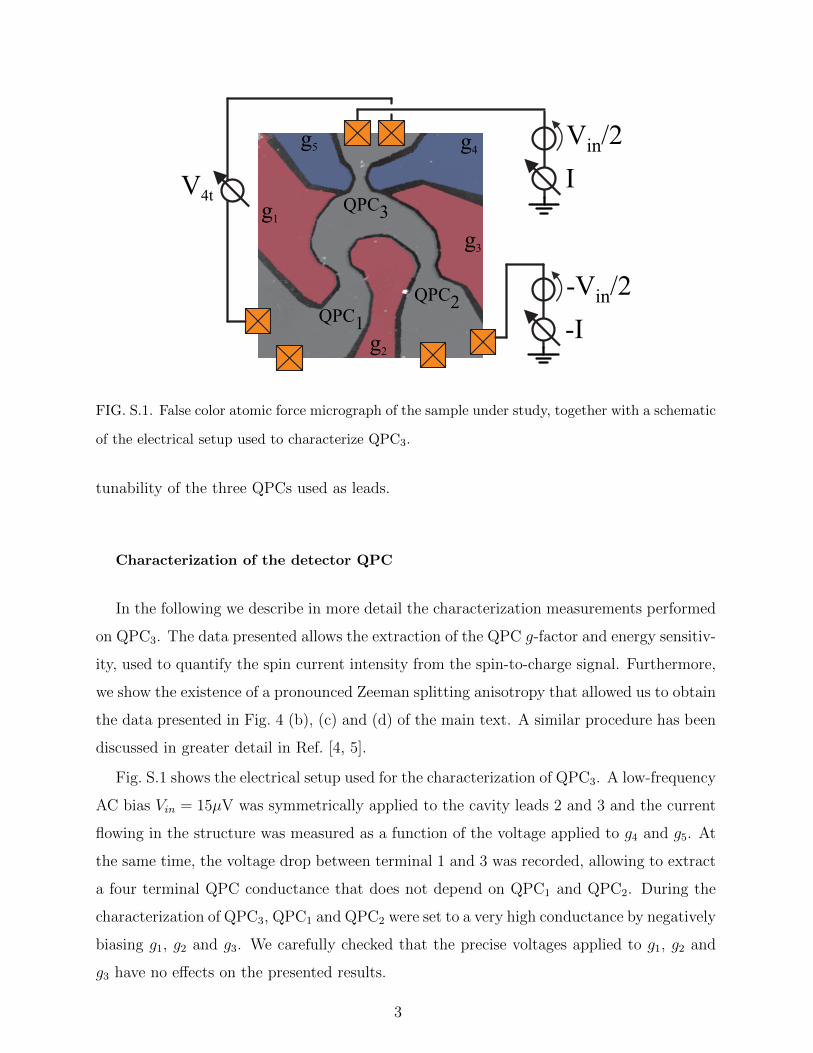
FIG. S.1. False color atomic force micrograph of the sample under study, together with a schematic
of the electrical setup used to characterize QPC3.
tunability of the three QPCs used as leads.
Characterization of the detector QPC
In the following we describe in more detail the characterization measurements performed
on QPC3. The data presented allows the extraction of the QPC g-factor and energy sensitiv-
ity, used to quantify the spin current intensity from the spin-to-charge signal. Furthermore,
we show the existence of a pronounced Zeeman splitting anisotropy that allowed us to obtain
the data presented in Fig. 4 (b), (c) and (d) of the main text. A similar procedure has been
discussed in greater detail in Ref. [4, 5].
Fig. S.1 shows the electrical setup used for the characterization of QPC3. A low-frequency
AC bias Vin = 15µV was symmetrically applied to the cavity leads 2 and 3 and the current
flowing in the structure was measured as a function of the voltage applied to g4 and g5. At
the same time, the voltage drop between terminal 1 and 3 was recorded, allowing to extract
a four terminal QPC conductance that does not depend on QPC1 and QPC2. During the
characterization of QPC3, QPC1 and QPC2 were set to a very high conductance by negatively
biasing g1, g2 and g3. We carefully checked that the precise voltages applied to g1, g2 and
g3 have no effects on the presented results.
3

Via finite bias measurements, we extracted the voltage dependent lever arm of g4 and g5.
The lever arm allows one to convert the gate voltage axis into energy and extract quantities
such as the g-factor and the energy sensitivity hω from a conductance measurement. For the
experiment under consideration, the determination of the lever arm is irrelevant if both hω
and the g-factor are extracted from the same conductance plot and in a narrow gate voltage
range, as we do here. In fact, as shown by Eq. (1) of the main text, the spin-to-charge
conversion amplitude is only given by the ratio hω/g that does not depend on the gate lever
arm.
Close to a conductanceG3 = e2/h, the relevant regime for the effects presented in the main
text, the lever arm was measured to be 4 meVV−1. We determined hω, i.e. the curvature
of the harmonic potential, by fitting a saddle point model [6] to the QPC conductance [7].
Since we do know the lever arm in this case, we can convert the curvature into energy units
by fitting the equation:
G(E) =2e2
hN
(1
1 + exp (2π(E − E0)/(hω))
), (S.1)
with the fitting parameters being a constant energy shift E0 and the potential curvature hω.
N is the mode number of the plateau under consideration, in this case N = 1.
The QPC is characterized by a strong g-factor anisotropy, typical for QPCs embedded in
2DHGs grown along the [001] crystallographic direction [4, 5]. The QPC transconductance
(numerical derivative with respect to gate voltage) is shown in Fig. S.2 for three different
magnetic field orientations. A finite spin splitting is present when the magnetic field is
oriented perpendicularly to the plane of the 2DHG (Fig. S.2(a)) or in the plane of the
2DHG and aligned along the QPC axis (Fig. S.2(c)). No spin splitting up to 12 T is visible
when the magnetic field is aligned in the plane of the 2DHG and perpendicular to the
QPC axis (Fig. S.2(b)). In order to use the QPC to detect a spin current via the spin-to-
charge conversion scheme, it is necessary to have a finite g-factor (see Eq. (1) of the main
text). In the present case, this is possible by performing the experiment with the magnetic
field oriented as in Fig. S.2(b). The g-factor is obtained from Fig. S.2(b) by tracking the
separation in gate voltage between spin split plateaus as a function of an in-plane magnetic
field. The gate voltage separation is then converted into Zeeman energy using the gate
dependent lever arm. For the first mode we find g = 0.27. In order to suppress the spin-
to-charge conversion efficiency, the magnetic field must be turned by 90 in the plane of
4
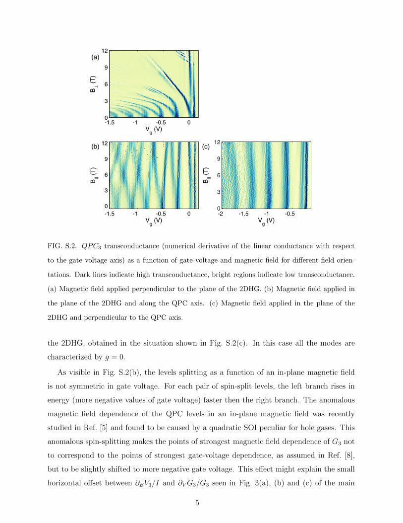
FIG. S.2. QPC3 transconductance (numerical derivative of the linear conductance with respect
to the gate voltage axis) as a function of gate voltage and magnetic field for different field orien-
tations. Dark lines indicate high transconductance, bright regions indicate low transconductance.
(a) Magnetic field applied perpendicular to the plane of the 2DHG. (b) Magnetic field applied in
the plane of the 2DHG and along the QPC axis. (c) Magnetic field applied in the plane of the
2DHG and perpendicular to the QPC axis.
the 2DHG, obtained in the situation shown in Fig. S.2(c). In this case all the modes are
characterized by g = 0.
As visible in Fig. S.2(b), the levels splitting as a function of an in-plane magnetic field
is not symmetric in gate voltage. For each pair of spin-split levels, the left branch rises in
energy (more negative values of gate voltage) faster then the right branch. The anomalous
magnetic field dependence of the QPC levels in an in-plane magnetic field was recently
studied in Ref. [5] and found to be caused by a quadratic SOI peculiar for hole gases. This
anomalous spin-splitting makes the points of strongest magnetic field dependence of G3 not
to correspond to the points of strongest gate-voltage dependence, as assumed in Ref. [8],
but to be slightly shifted to more negative gate voltage. This effect might explain the small
horizontal offset between ∂BV3/I and ∂VG3/G3 seen in Fig. 3(a), (b) and (c) of the main
5
−0.5 −0.4 −0.3 −0.2 −0.1 0−40
−20
0
20
40
60
80
Vg3,g4
(V)
∂ B V
3/I
(Ω
T−
1)
T = 109 mK
T = 250 mK
T = 530 mK
0.5 5 50
10
20
40
80
I (nA)
∂ B V
3/I
(Ω
T−
1)
(a) (b)
I = 4 nAT = 109 mKV
g3,g4 = −0.115 V
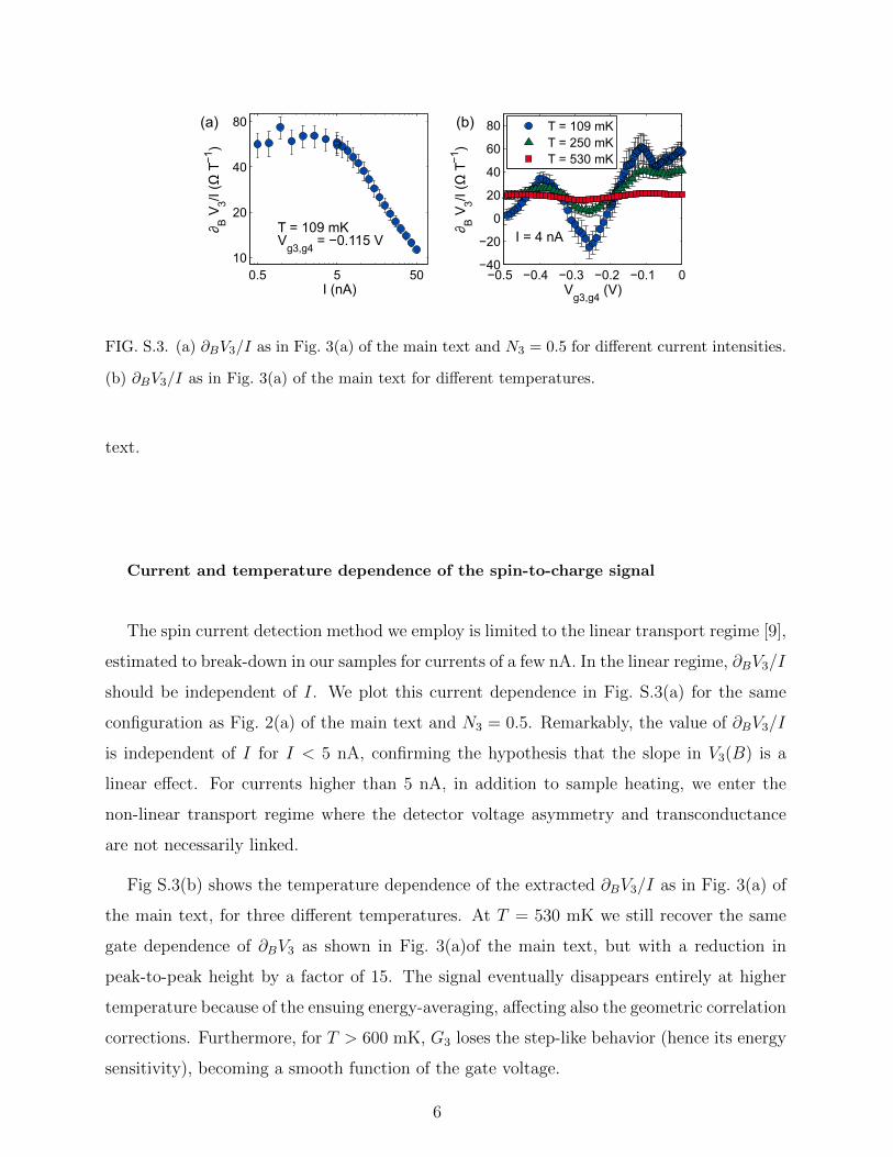
FIG. S.3. (a) ∂BV3/I as in Fig. 3(a) of the main text and N3 = 0.5 for different current intensities.
(b) ∂BV3/I as in Fig. 3(a) of the main text for different temperatures.
text.
Current and temperature dependence of the spin-to-charge signal
The spin current detection method we employ is limited to the linear transport regime [9],
estimated to break-down in our samples for currents of a few nA. In the linear regime, ∂BV3/I
should be independent of I. We plot this current dependence in Fig. S.3(a) for the same
configuration as Fig. 2(a) of the main text and N3 = 0.5. Remarkably, the value of ∂BV3/I
is independent of I for I < 5 nA, confirming the hypothesis that the slope in V3(B) is a
linear effect. For currents higher than 5 nA, in addition to sample heating, we enter the
non-linear transport regime where the detector voltage asymmetry and transconductance
are not necessarily linked.
Fig S.3(b) shows the temperature dependence of the extracted ∂BV3/I as in Fig. 3(a) of
the main text, for three different temperatures. At T = 530 mK we still recover the same
gate dependence of ∂BV3 as shown in Fig. 3(a)of the main text, but with a reduction in
peak-to-peak height by a factor of 15. The signal eventually disappears entirely at higher
temperature because of the ensuing energy-averaging, affecting also the geometric correlation
corrections. Furthermore, for T > 600 mK, G3 loses the step-like behavior (hence its energy
sensitivity), becoming a smooth function of the gate voltage.
6

Spin-to-charge conversion
We review here the theoretical basis for the spin-to-charge conversion effect in a three-
terminal mesoscopic cavity as the one depicted in Fig. 1(a) of the main text. We extend the
theory presented in Ref. [8] to prove the proportionality between ∂BV3/I and ∂VG3/G3.
The cavity under consideration has three contacts (labeled 1,2 and 3), and each of them
is at a voltage Vi and carries Ni spin degenerate modes. We consider the situation where
N3 ≤ 1 and N1, N2 1. By applying a voltage bias V2−V1 between leads 1 and 2, a charge
current I will flow in the cavity. If contact 3 is grounded, a charge current I(0)3 will flow in
it. In the following we are interested in the situation in which no charge current flows in
contact 3 at zero magnetic field. This situation can be achieved either by applying a voltage
V3 that sets I(0)3 to zero at zero magnetic field, or by leaving it floating and connected to a
volt meter that measures V3. In the first case, the application of a magnetic field will make
the current vary from zero, in the second case the current will always remain zero and the
measured V3 will vary. As we will show in the following, the zero field spin current I(S)3 in
contact 3 is directly proportional to the zero-field derivative of I3, or V3, with respect to the
in-plane magnetic field:
I(S)3 =
hω
πµ∂BI
(0)3 |B=0, (S.2)
I(S)3 =
hω
πµ
e2
h
(2− T (0)
33
)∂BV3|B=0, (S.3)
where hω is the magnetic field energy sensitivity, µ = gµB/2 is the electron magnetic moment
and (2 − T (0)33 ) is the charge transmission coefficient of contact 3. These QPC parameters
are easily measured experimentally.
In the following theoretical treatment we do not include the presence of any orbital effect.
The latter assumption is well justified if no out-of-plane magnetic field is applied. An in-
plane field can give rise to other orbital effects [10] which will not be accounted for in this
section, assuming that these are small enough. We will always consider that the voltages
applied to the system are within the linear response regime (i.e. small compared to other
energy scales). The generic current I(α)i at a contact i can be calculated using Landauer-
Buttiker formalism, resulting in:
7

Iαi =∑j
(2Njδijδα0 − T (α)
ij
)Vj, (S.4)
where i = 1, 2, 3 denotes the leads and α = 0, x, y, z denotes the spin polarization of the
current. The generic transmission coefficient is:
T(α)ij =
∑m∈i,n∈j
Tr(t†mnσ
(α)tmn), (S.5)
where σ(α) are spin matrices, with σ(0) the identity matrix. The 2× 2 matrices tmn indicate
the probability of an electron entering the cavity from the n-th mode of QPC j to exit the
cavity from the m-th mode of QPC i, their elements tσσ′
m,n take into account spin flipping. It
can be shown that the transmission coefficients for charge and spin are:
τ(0)ij =
∑σσ′
τσσ′
ij (S.6)
, τ(S)ij =
∑σσ′
στσσ′
ij . (S.7)
The transmission probabilities from contact 1 or 2 to contact 3 are assumed to take the
form:
T σσ′
3i (B) = τσσ′
3i (B)Γ (EF − σµB) , (S.8)
hence they can be separated into a spin dependent part and an energy dependent part. The
spin affects the second term only via the Zeeman energy. In Eq. (S.8) it was assumed that
the QPC has high energy sensitivity, hence Γ (EF − σµB) varies faster than τσσ′
3i (B) with
B. τσσ′
3i (B) are phenomenological parameters, describing the spin transmission of the QPC
when it is fully open. Eq. (S.8) is valid only in the limit when an electron reflected back in
the cavity from contact 3 has a negligible probability to come back to contact 3 again. This
limit is achieved when N1, N2 N3.
Using Landauer-Buttiker expressions for charge and spin current through contact 3 one
has:
I(0)3 =
e2
h
(T
(0)31 (V3 − V1) + T
(0)32 (V3 − V2)
), (S.9)
I(S)3 =
e2
h
(T
(S)31 (V3 − V1) + T
(S)32 (V3 − V2)
). (S.10)
Imposing I3(0) = 0 allows to find an analytical form for the spin current:
8
V3 =(T
(0)31 V1T
(0)32 V2
)/(T
(0)31 + T
(0)32
), (S.11)
I(S)3 =
e2
h
(T
(S)31 (V3 − V1) + T
(S)32 (V3 − V2)
). (S.12)
Equations (S.2) and (S.3) are obtained by evaluating ∂BI3(0)|B=0with constant V3 and
∂BV3|B=0 for I(0)3 = 0, respectively. For obtaining a simpler analytical form of these expres-
sions, we will make an assumption of the specific form of the QPC transmission Γ, though
the results of this section do not qualitatively depend on this choice. We choose the saddle
point potential model, which gives the QPC energy dependent transmission probability as
[6]:
Γ(EF , Vg, B) =1
1 + exp (−2π (EF − αVg − σµB) /hω). (S.13)
The partial derivative of the QPC transmission with respect to magnetic field is:
∂BΓ(EF , Vg, B) = σµ∂VgΓ(EF , Vg, B). (S.14)
This allows us to write the magnetic field derivative of the charge transmission coefficients
T(0)3i in terms of spin transmission coefficients T
(S)3i :
∂BT(0)3i = ∂B
∑σσ′
T σσ′
ij |B=0 (S.15)
=∑σσ′
τσσ′
ij ∂BΓ(EF , Vg, 0)|B=0 (S.16)
=∑σσ′
τσσ′
ij σµ∂VgΓ(EF , Vg, 0)|B=0 (S.17)
=∑σσ′
τσσ′
ij σµΓ(EF , Vg, 0)∂VgΓ(EF , Vg, 0)|B=0
Γ(EF , Vg, 0)(S.18)
= µT(S)3i
∂VgΓ(EF , Vg, 0)|B=0
Γ(EF , Vg, 0). (S.19)
In the middle of the first slope in the QPC conductance, the energy sensitivity is maximal
and it gives (Vg = EF ):
∂VgΓ(EF , Vg, 0)|B=0
Γ(EF , Vg, 0)= − π
hω. (S.20)
9

With this, the zero-field derivative of the charge current is (V1, V2, V3 are constant):
∂BI(0)3 |B=0 = −e
2
h
(∂BT
(0)31 (V3 − V1) + ∂BT
(0)32 (V 3− V2)
)(S.21)
= −e2
h
(µ∂VgΓ(EF , Vg, 0)|B=0
Γ(EF , Vg, 0)
)(T
(S)31 (V3 − V1) + T
(S)32 (V3 − V2)
)(S.22)
= −µ∂VgΓ(EF , Vg, 0)|B=0
Γ(EF , Vg, 0)I(S)3 (S.23)
=πµ
hωI(S)3 . (S.24)
Finally, Eq (S.2) is obtained solving Eq. (S.24) for I(S)3 . Similarly, the zero field derivative
of V3 is:
∂BV3|B=0 = −µ∂VgΓ(EF , Vg, 0)|B=0
Γ(EF , Vg, 0)
1
2− T (0)33
h
e2I(S)3 . (S.25)
In the point of highest energy sensitivity we have:
∂BV3|B=0 =h
e2πµ
hω
1
2− T (0)33
I(S)3 , (S.26)
which results in Eq. (S.3) upon solving for I(S)3 .
It is interesting, in the light of our experimental results, to investigate the behavior of
∂BV3|B=0 around the point of highest energy sensitivity. 2− T (0)33 is the exact expression for
the charge current transmission coefficient of contact 3. It can be approximated as (see Eq.
(S.8)):
2− T (0)33 = T
(0)31 + T
(0)32 =
∑σσ′
(τσσ
′
31 + τσσ′
32
)Γ(EF , V g, B). (S.27)
We can apply the approximation from Eq. (S.8) to Eq. (S.10), finding a relation between
I(S)3 and Γ:
I(S)3 = −e
2
h
(∑σσ′
τσσ′
31 (V1 − V3) +∑σσ′
τσσ′
32 (V2 − V3)
)Γ(EF , Vg, B). (S.28)
Combining the last three equations we get the expression:
∂BV3|B=0 = µC∂VgΓ(EF , Vg, 0)|B=0
Γ(EF , Vg, 0), (S.29)
where C is a prefactor containing the voltages Vi and the coefficients τσσ′
3i . It is assumed
to be constant with respect to gate voltage. The results obtained here can be summarized
with the following proportionality relation:
10

∂BV3|B=0 ∝∂VgΓ(EF , Vg, 0)|B=0
Γ(EF , Vg, 0). (S.30)
It is worth reminding that Eq. (S.30) is valid in the limit N1, N2 N3 and N3 ≤ 1 and the
coefficients τσσ′
3i are supposed to weakly depend on magnetic field.
In the absence of SOI, reversing the magnetic field direction reverses the sign of the spin
polarization S. In this case τ(0)3i (B) = τ
(0)3i (−B) and τ
(S)3i (B) = −τ (S)3i (−B) (see Eq. (S.6) and
(S.7)). Since Γ(EF , Vg, B) is an even function of B, it results that T σσ′
3i (B) = −T σσ′3i (−B),
and IS3 (0) = 0 (see Eq. (S.12)): in the absence of SOI, both ∂BI(0)3 and ∂BV3 vanish.
∗ Present Address: Center for Quantum Devices, Niels Bohr Institute, University of
Copenhagen, 2100 Copenhagen, Denmark; email: [email protected]; homepage:
www.nanophys.ethz.ch
[1] F. Nichele, A. N. Pal, R. Winkler, C. Gerl, W. Wegscheider, T. Ihn, and K. Ensslin, Phys.
Rev. B 89, 081306 (2014).
[2] R. Winkler, Spin-Orbit Coupling Effects in Two-Dimensional Electron and Hole Systems,
Springer Tracts in Modern Physics, Vol. 191 (Springer-Verlag, Berlin, 2003).
[3] I. Adagideli, P. Jacquod, M. Scheid, M. Duckheim, D. Loss, and K. Richter, Phys. Rev. Lett.
105, 246807 (2010).
[4] A. Srinivasan, L. A. Yeoh, O. Klochan, T. P. Martin, J. C. H. Chen, A. P. Micolich, A. R.
Hamilton, D. Reuter, and A. D. Wieck, Nano Letters, Nano Lett. 13, 148 (2012).
[5] F. Nichele, S. Chesi, S. Hennel, A. Wittmann, C. Gerl, W. Wegscheider, D. Loss, T. Ihn, and
K. Ensslin, Phys. Rev. Lett. 113, 046801 (2014).
[6] M. Buttiker, Phys. Rev. B 41, 7906 (1990).
[7] C. Rossler, S. Baer, E. de Wiljes, P.-L. Ardelt, T. Ihn, K. Ensslin, C. Reichl, and W. Wegschei-
der, New Journal of Physics 13, 113006 (2011).
[8] P. Stano and P. Jacquod, Phys. Rev. Lett. 106, 206602 (2011).
[9] P. Stano, J. Fabian, and P. Jacquod, Phys. Rev. B 85, 241301 (2012).
[10] D. M. Zumbuhl, J. B. Miller, C. M. Marcus, V. I. Fal’ko, T. Jungwirth, and J. S. Harris,
Phys. Rev. B 69, 121305 (2004).
11