geometric programming and its applications to eda problems
TRANSCRIPT

Geometric Programming and
Its Applications to EDA Problems
Stephen Boyd Seung Jean Kim S. S. Mohan
Boyd, Kim, & Mohan, DATE Tutorial 2005

Outline
• Basic approach
• Geometric programming & generalized geometric programming
• Digital circuit design applications
• Analog and RF circuit design applications
• Monomial and posynomial fitting
• Conclusions
Boyd, Kim, & Mohan, DATE Tutorial 2005 1

Basic Approach

Basic approach
1. formulate circuit design problem as geometric program (GP), anoptimization problem with special form
2. solve GP using specialized, tailored method
• this tutorial focuses on step 1 (a.k.a. GP modeling)
• step 2 is technology
Boyd, Kim, & Mohan, DATE Tutorial 2005 2

Why?
• we can solve even large GPs very effectively, using recently developedmethods
• so once we have a GP formulation, we can solve circuit design problemeffectively
we will see that
• GP is especially good at handling a large number of concurrentconstraints
• GP formulation is useful even when it is approximate
Boyd, Kim, & Mohan, DATE Tutorial 2005 3

Trade-offs in optimization
• general trade-off between generality and effectiveness
• generality
– number of problems that can be handled– accuracy of formulation– ease of formulation
• effectiveness
– speed of solution, scale of problems that can be handled– global vs. local solutions– reliability, baby-sitting, starting point
Boyd, Kim, & Mohan, DATE Tutorial 2005 4

Example: least-squares vs. simulated annealing
least-squares
• large problems reliably (globally) solved quickly
• no initial point, no algorithm parameter tuning
• solves very restricted problem form
• with tricks and extensions, basis of vast number of methods that work(control, filtering, regression, . . . )
simulated annealing
• can be applied to any problem (more or less)
• slow, needs tuning, babysitting; not global in practice
• method of choice for some problems you can’t handle any other way
Boyd, Kim, & Mohan, DATE Tutorial 2005 5

Where GP fits in
somewhere in between, closer to least-squares . . .
• like least-squares, large problems can be solved reliably (globally), nostarting point, tuning, . . .
• solves a class of problems broader than least-squares, less general thansimulated annealing
• formulation takes effort, but is fun and has high payoff
Boyd, Kim, & Mohan, DATE Tutorial 2005 6

Geometric Programming &Generalized Geometric Programming
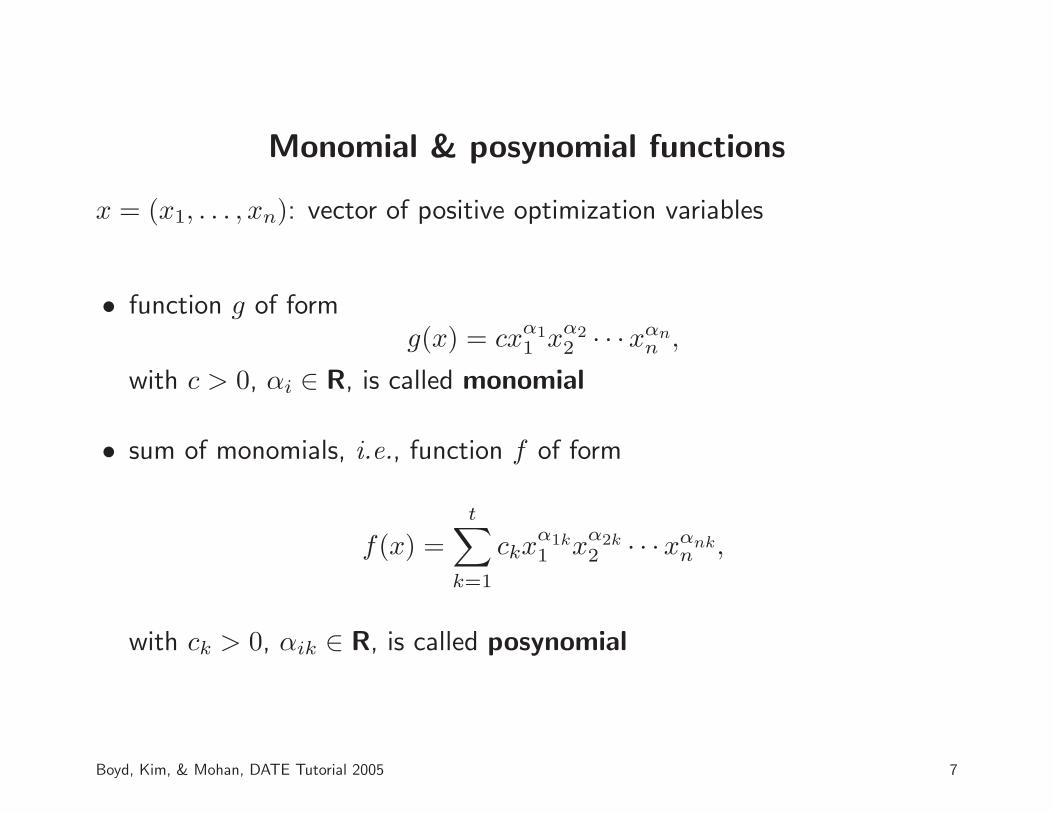
Monomial & posynomial functions
x = (x1, . . . , xn): vector of positive optimization variables
• function g of formg(x) = cxα1
1 xα22 · · ·xαn
n ,
with c > 0, αi ∈ R, is called monomial
• sum of monomials, i.e., function f of form
f(x) =
t∑
k=1
ckxα1k1 x
α2k2 · · ·xαnk
n ,
with ck > 0, αik ∈ R, is called posynomial
Boyd, Kim, & Mohan, DATE Tutorial 2005 7

Examples
with x, y, z variables,
• 0.23, 2z√
x/y, 3x2y−.12z are monomials (hence also posynomials)
• 0.23 + x/y, 2(1 + xy)3, 2x + 3y + 2z are posynomials
• 2x + 3y − 2z, x2 + tanx are neither
Boyd, Kim, & Mohan, DATE Tutorial 2005 8
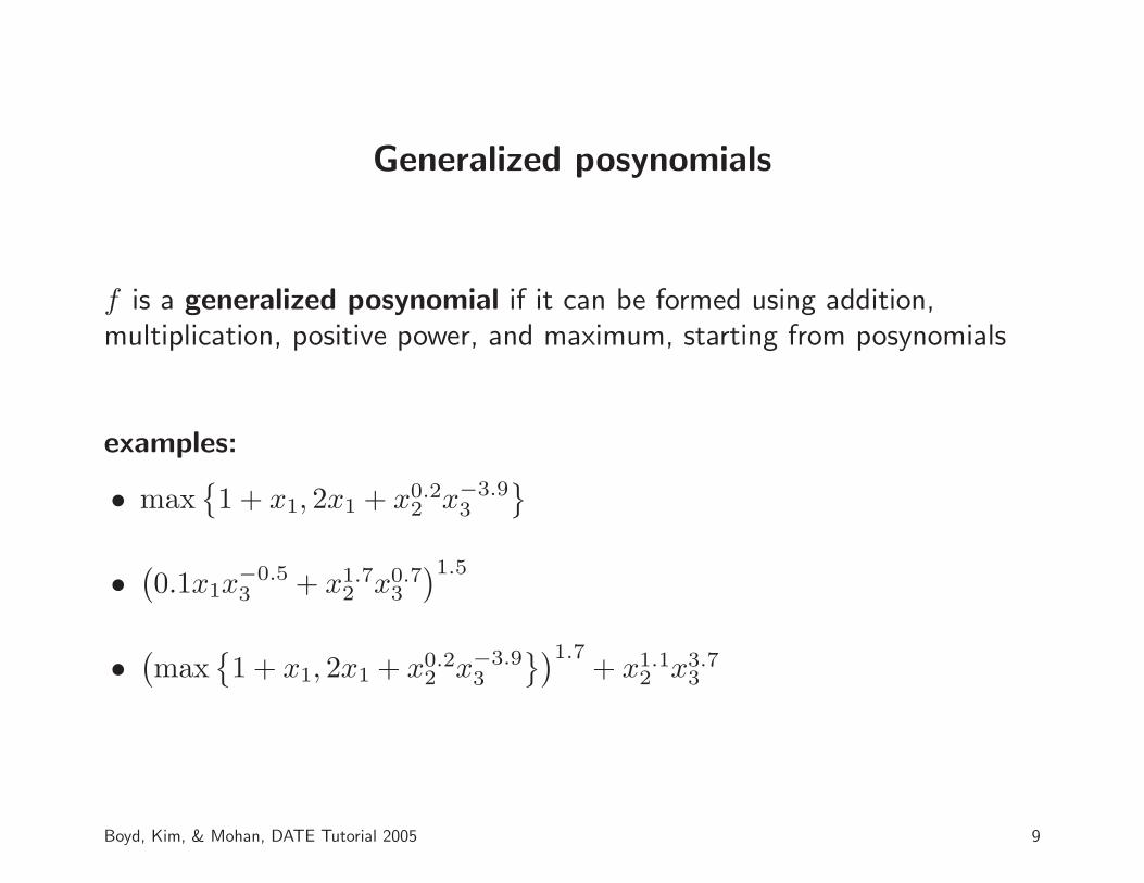
Generalized posynomials
f is a generalized posynomial if it can be formed using addition,multiplication, positive power, and maximum, starting from posynomials
examples:
• max1 + x1, 2x1 + x0.2
2 x−3.93
•(0.1x1x
−0.53 + x1.7
2 x0.73
)1.5
•(max
1 + x1, 2x1 + x0.2
2 x−3.93
)1.7+ x1.1
2 x3.73
Boyd, Kim, & Mohan, DATE Tutorial 2005 9

Composition rules
• monomials closed under product, division, positive scaling, power,inverse
• posynomials closed under sum, product, positive scaling, division bymonomial, positive integer power
• generalized posynomials closed under sum, product, max, positivescaling, division by monomial, positive power
Boyd, Kim, & Mohan, DATE Tutorial 2005 10

Generalized geometric program (GGP)
minimize f0(x)subject to fi(x) ≤ 1, i = 1, . . . , m
gi(x) = 1, i = 1, . . . , p
fi are generalized posynomials, gi are monomials
• called geometric program (GP) when fi are posynomials
• a highly nonlinear constrained optimization problem
Boyd, Kim, & Mohan, DATE Tutorial 2005 11

GP example
• maximize volume of box with width w, height h, depth d
• subject to limits on wall and floor areas, aspect ratios h/w, d/w
maximize hwdsubject to 2(hw + hd) ≤ Awall, wd ≤ Aflr
α ≤ h/w ≤ β, γ ≤ d/w ≤ δ
in standard GP form:
minimize h−1w−1d−1
subject to (2/Awall)hw + (2/Awall)hd ≤ 1, (1/Aflr)wd ≤ 1αh−1w ≤ 1, (1/β)hw−1 ≤ 1γwd−1 ≤ 1, (1/δ)w−1d ≤ 1
Boyd, Kim, & Mohan, DATE Tutorial 2005 12

GGP example: Floor planning
• choose cell widths, heights
• fixed cell areas
• (1 left of 2) above (3 left of 4)
• aspect ratio constraints
• minimize bounding box area
w1 w2
w3w4
w
h1 h2
h3 h4
h
minimize hwsubject to hiwi = Ai, 1/αmax ≤ hi/wi ≤ αmax,
maxh1, h2 + maxh3, h4 ≤ h,maxw1 + w2, w3 + w4 ≤ w
. . . a GGP
Boyd, Kim, & Mohan, DATE Tutorial 2005 13

Trade-off analysis
(no equality constraints, for simplicity)
• form perturbed version of original GP, with changed righthand sides:
minimize f0(x)subject to fi(x) ≤ ui, i = 1, . . . , m
• ui > 1 (ui < 1) means ith constraint is relaxed (tightened)
• let p(u) be optimal value of perturbed problem
• plot of p vs. u is (globally) optimal trade-off surface (of objectiveagainst constraints)
Boyd, Kim, & Mohan, DATE Tutorial 2005 14

Trade-off curves for maximum volume box example
Afloor
V
Awall = 100Awall = 100
Awall = 1000Awall = 1000
Awall = 10000Awall = 10000
10 102 10310
102
103
104
105
• maximum volume V vs. Aflr, for Awall = 100, 1000, 10000
• h/w, d/w aspect ratio limits 0.5, 2
Boyd, Kim, & Mohan, DATE Tutorial 2005 15

Sensitivity analysis
• optimal sensitivity of ith constraint is
Si =∂p/p
∂ui/ui
∣∣∣∣u=1
• Si predicts fractional change in optimal objective value if ith constraintis (slightly) relaxed or tightened
• very useful in practice; give quantitative measure of how tight a bindingconstraint is
• when we solve a GP we get all optimal sensitivities at no extra cost
Boyd, Kim, & Mohan, DATE Tutorial 2005 16
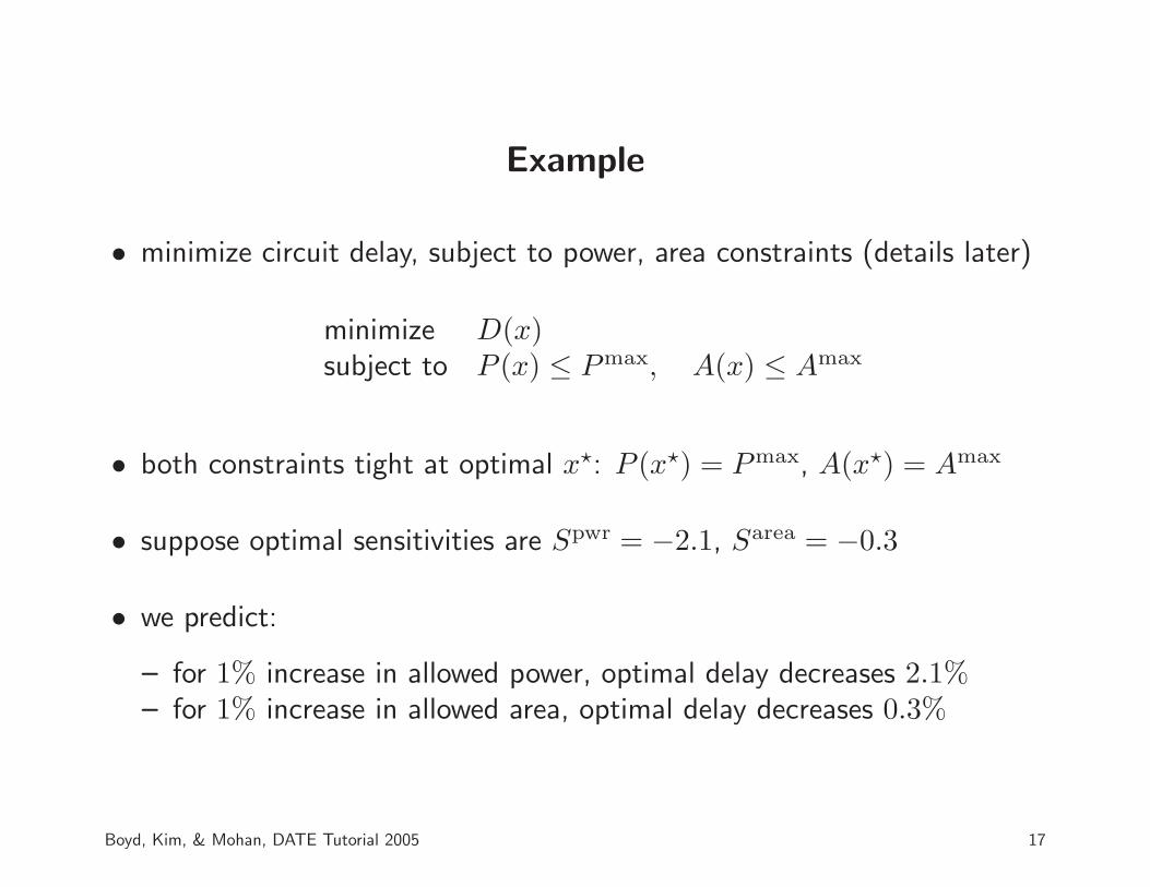
Example
• minimize circuit delay, subject to power, area constraints (details later)
minimize D(x)subject to P (x) ≤ Pmax, A(x) ≤ Amax
• both constraints tight at optimal x⋆: P (x⋆) = Pmax, A(x⋆) = Amax
• suppose optimal sensitivities are Spwr = −2.1, Sarea = −0.3
• we predict:
– for 1% increase in allowed power, optimal delay decreases 2.1%– for 1% increase in allowed area, optimal delay decreases 0.3%
Boyd, Kim, & Mohan, DATE Tutorial 2005 17

GP and GGP attributes
• after log transform of variables/constraints, they become convexproblems
• can convert GGP to GP, e.g., f(x) + maxg(x), h(x) ≤ 1 becomes
f(x) + t ≤ 1, g(x)/t ≤ 1, h(x)/t ≤ 1
where t is new (dummy) variable
• conversion tricks can be automated
– parser scans problem description, forms GP– efficient GP solver solves GP– solution transformed back (dummy variables eliminated)
Boyd, Kim, & Mohan, DATE Tutorial 2005 18

How GPs are solved
the practical answer: none of your business
more politely: you don’t need to know
it’s technology:
• good algorithms are known
• good software implementations are available
Boyd, Kim, & Mohan, DATE Tutorial 2005 19

How GPs are solved
• work with log of variables: yi = log xi
• take log of monomials/posynomials to get
minimize log f0(ey)
subject to log fi(ey) ≤ 0, i = 1, . . . , m
log gi(ey) = 0, i = 1, . . . , p
• log fi(ey) are (smooth) convex functions
• log gi(ey) are affine functions, i.e., linear plus a constant
• solve (nonlinear) convex optimization problem above usinginterior-point method
Boyd, Kim, & Mohan, DATE Tutorial 2005 20

Current state of the art
• basic interior-point method that exploits sparsity, generic GP structure
• approaching efficiency of linear programming solver
– sparse 1000 vbles, 10000 monomial terms: few seconds– sparse 10000 vbles, 100000 monomial terms: minute– sparse 106 vbles, 107 monomial terms: hour
(these are order-of-magnitude estimates, on simple PC)
Boyd, Kim, & Mohan, DATE Tutorial 2005 21
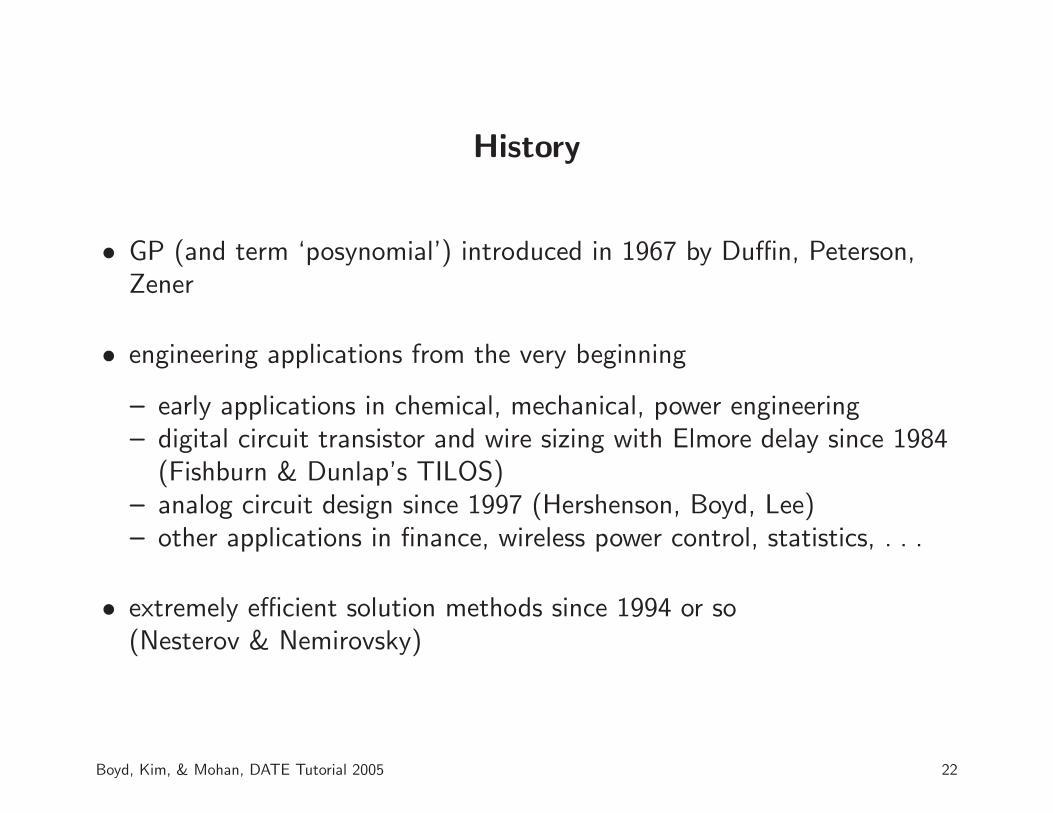
History
• GP (and term ‘posynomial’) introduced in 1967 by Duffin, Peterson,Zener
• engineering applications from the very beginning
– early applications in chemical, mechanical, power engineering– digital circuit transistor and wire sizing with Elmore delay since 1984
(Fishburn & Dunlap’s TILOS)– analog circuit design since 1997 (Hershenson, Boyd, Lee)– other applications in finance, wireless power control, statistics, . . .
• extremely efficient solution methods since 1994 or so(Nesterov & Nemirovsky)
Boyd, Kim, & Mohan, DATE Tutorial 2005 22
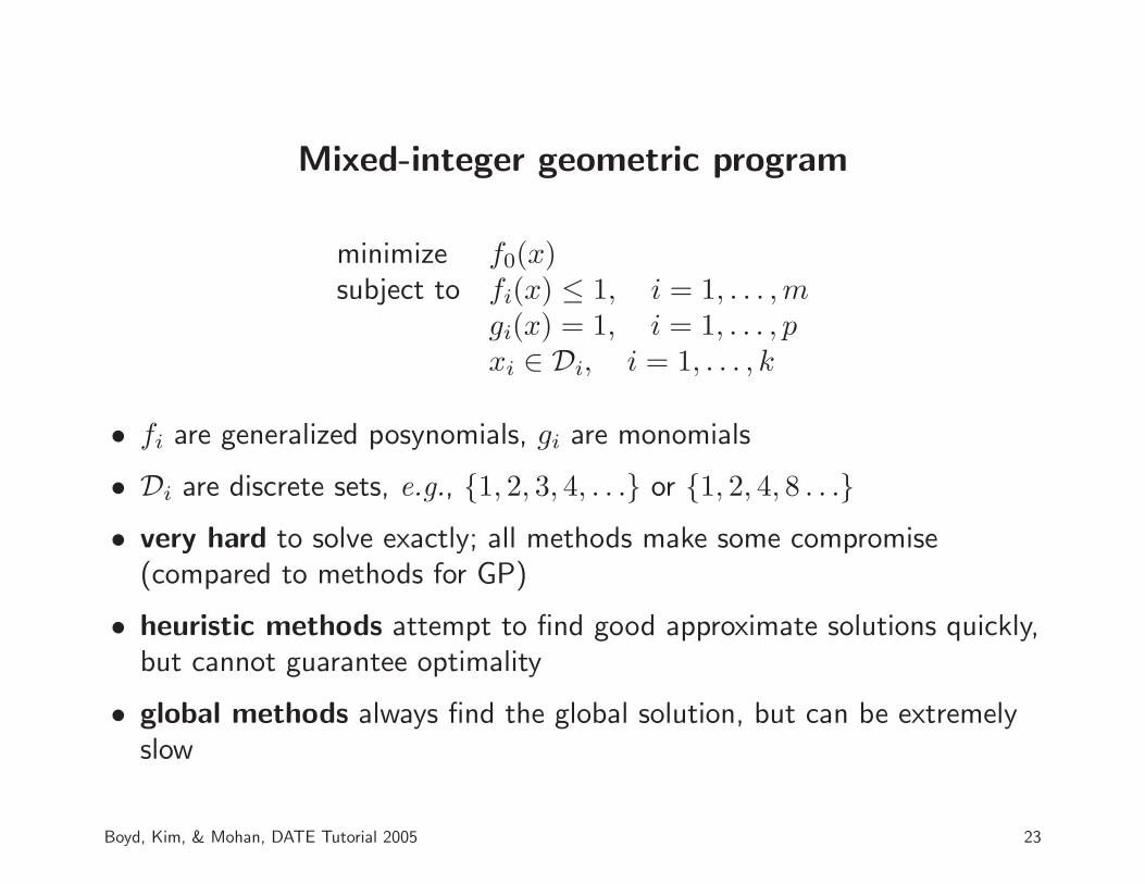
Mixed-integer geometric program
minimize f0(x)subject to fi(x) ≤ 1, i = 1, . . . ,m
gi(x) = 1, i = 1, . . . , pxi ∈ Di, i = 1, . . . , k
• fi are generalized posynomials, gi are monomials
• Di are discrete sets, e.g., 1, 2, 3, 4, . . . or 1, 2, 4, 8 . . .• very hard to solve exactly; all methods make some compromise
(compared to methods for GP)
• heuristic methods attempt to find good approximate solutions quickly,but cannot guarantee optimality
• global methods always find the global solution, but can be extremelyslow
Boyd, Kim, & Mohan, DATE Tutorial 2005 23

Digital Circuit Design Applications
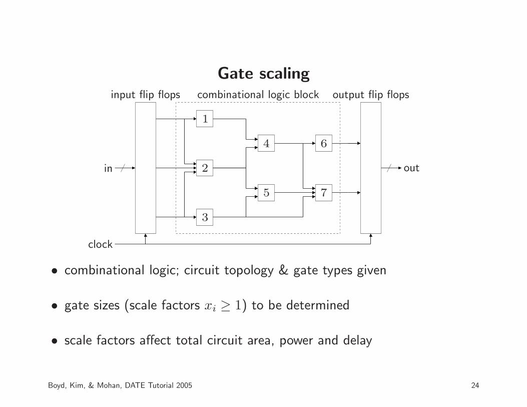
Gate scaling
1
2
3
4
5
6
7
input flip flops output flip flops
in out
clock
combinational logic block
• combinational logic; circuit topology & gate types given
• gate sizes (scale factors xi ≥ 1) to be determined
• scale factors affect total circuit area, power and delay
Boyd, Kim, & Mohan, DATE Tutorial 2005 24
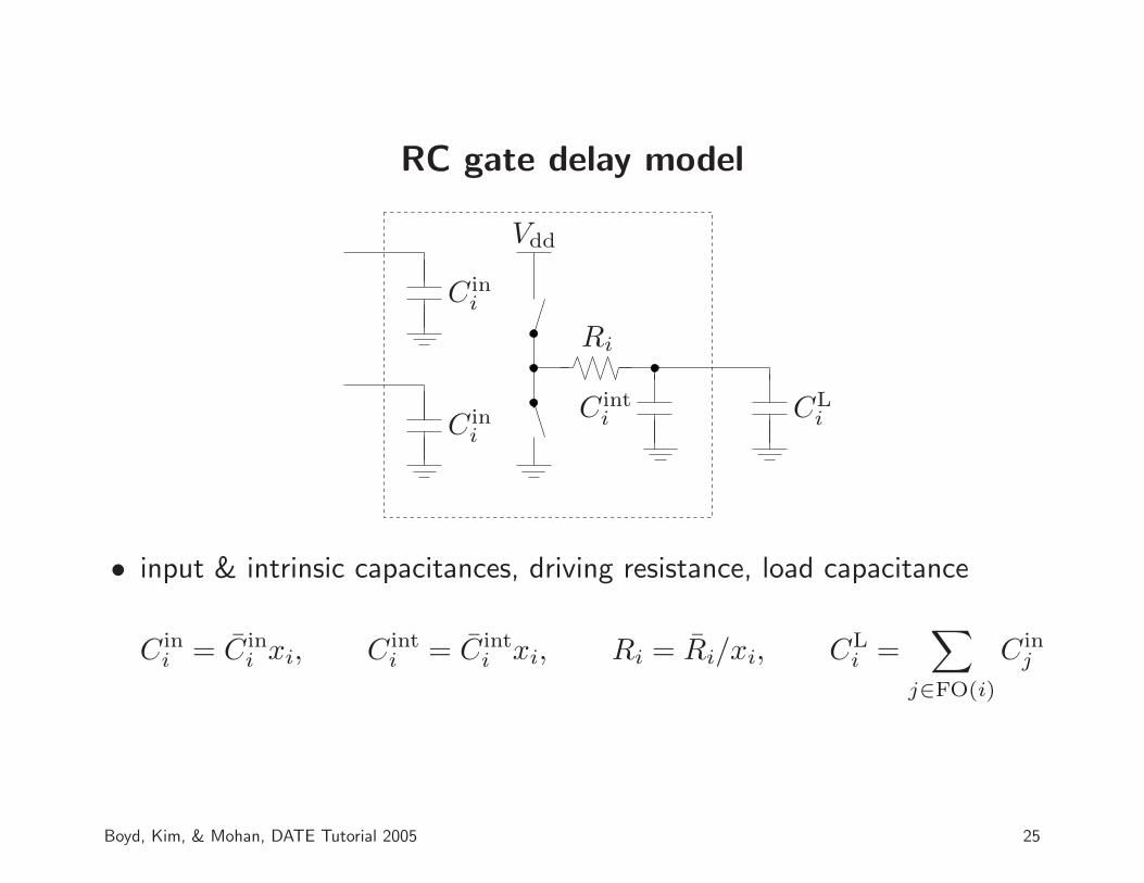
RC gate delay model
PSfrag
Ri
Vdd
C ini
C ini
C inti CL
i
• input & intrinsic capacitances, driving resistance, load capacitance
C ini = C in
i xi, C inti = C int
i xi, Ri = Ri/xi, CLi =
∑
j∈FO(i)
C inj
Boyd, Kim, & Mohan, DATE Tutorial 2005 25

RC gate model
• RC gate delay:
Di = 0.69Ri(CLi + C int
i ) = 0.69
RiCini + (Ri/xi)
∑
j∈FO(i)
C inj xj
• Di are posynomials (of scale factors)
Boyd, Kim, & Mohan, DATE Tutorial 2005 26

Path and circuit delay
1
2
3
4
5
6
7
• delay of a path: sum of delays of gates on path. . . posynomial
• circuit delay: maximum delay over all paths. . . generalized posynomial
Boyd, Kim, & Mohan, DATE Tutorial 2005 27

Area & power
• total circuit area: A = x1A1 + · · · + xnAn
• total power is P = Pdyn + Pstat
– dynamic power Pdyn =
n∑
i=1
fi(CLi + C int
i )V 2dd
fi is gate switching frequency
– static power Pstat =
n∑
i=1
xiIleaki Vdd
I leaki is leakage current (average over input states) of unit scaled gate
• A and P are linear functions of x, with positive coefficients, henceposynomials
Boyd, Kim, & Mohan, DATE Tutorial 2005 28

Basic gate scaling problem
minimize Dsubject to P ≤ Pmax, A ≤ Amax
1 ≤ xi, i = 1, . . . , n
. . . a GGP
extensions/variations:
• minimize area, power, or some combination
• maximize clock frequency subject to area, power limits
• add other constraints
• optimal trade-off of area, power, delay
Boyd, Kim, & Mohan, DATE Tutorial 2005 29

Clock frequency maximization
• fclk is variable
• timing requirement: D ≤ 0.8/fclk
(20% margin for flip-flop delay, setup time, clock skew . . . )
• P is posynomial of scalings and fclk, assuming fi scale with fclk
maximize fclk
subject to P ≤ Pmax, A ≤ Amax, (1/0.8)Dfclk ≤ 1,1 ≤ xi, i = 1, . . . , n
. . . a GGP
Boyd, Kim, & Mohan, DATE Tutorial 2005 30

Example: 32-bit Ladner-Fisher adder
• 451 gates (scale factors), 5 gate types, 64 inputs, 32 outputs
• logical effort gate delay model parameters:
gate type C in C int R A I leak
INV 3 3 0.48 3 0.006NAND2 4 6 0.48 8 0.007NOR2 5 6 0.48 10 0.009AOI21 6 7 0.48 17 0.003OAI21 6 7 0.48 16 0.003
• time unit is τ , delay of min-size inverter (0.69 · 0.48 · 3 = 1)
• area (total width) unit is width of NMOS in min-size inverter
Boyd, Kim, & Mohan, DATE Tutorial 2005 31
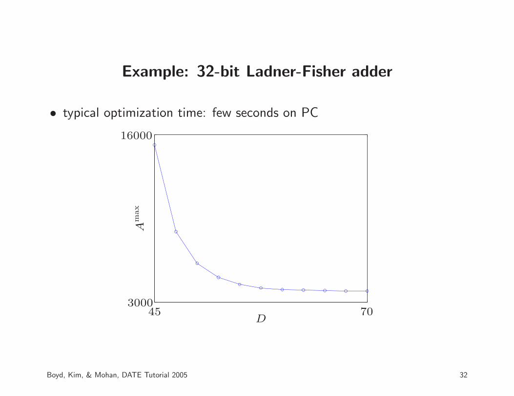
Example: 32-bit Ladner-Fisher adder
• typical optimization time: few seconds on PC
D
Am
ax
45 703000
16000
Boyd, Kim, & Mohan, DATE Tutorial 2005 32

32-bit Ladner-Fisher adder with discrete scale factors
• add constraints xi ∈ 1, 2, 4, 8, 16, . . .• simple rounding of optimal continuous scalings
D
Am
ax
45 703000
16000 simple roundingoptimal continuous
Boyd, Kim, & Mohan, DATE Tutorial 2005 33

Sparse GP gate scaling problem
minimize Dsubject to Tj ≤ D for j an output gate
Tj + Di ≤ Ti for j ∈ FI(i)P ≤ Pmax, A ≤ Amax
1 ≤ xi, i = 1, . . . , n
• Ti are upper bounds on signal arrival times
• extremely sparse GP; can be solved very efficiently
Boyd, Kim, & Mohan, DATE Tutorial 2005 34

Better (generalized posynomial) models
can greatly improve model, while retaining GP compatibility(hence efficient global solution)
• area, delay, power can be any generalized posynomials of scale factors,e.g.,
Di = ai + bi(CLi )1.05x−0.9
i , Pi = ci + di(CLi )1.2 + eix
1.1i
• these can be found by more refined analysis, or fitting generalizedposynomials to simulation/characterization data
Boyd, Kim, & Mohan, DATE Tutorial 2005 35
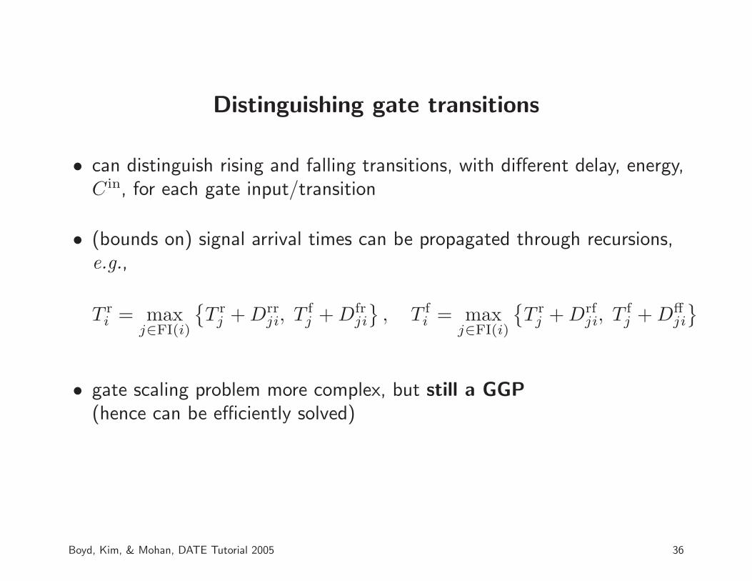
Distinguishing gate transitions
• can distinguish rising and falling transitions, with different delay, energy,C in, for each gate input/transition
• (bounds on) signal arrival times can be propagated through recursions,e.g.,
T ri = max
j∈FI(i)
T r
j + Drrji, T f
j + Dfrji
, T f
i = maxj∈FI(i)
T r
j + Drfji, T f
j + Dffji
• gate scaling problem more complex, but still a GGP(hence can be efficiently solved)
Boyd, Kim, & Mohan, DATE Tutorial 2005 36
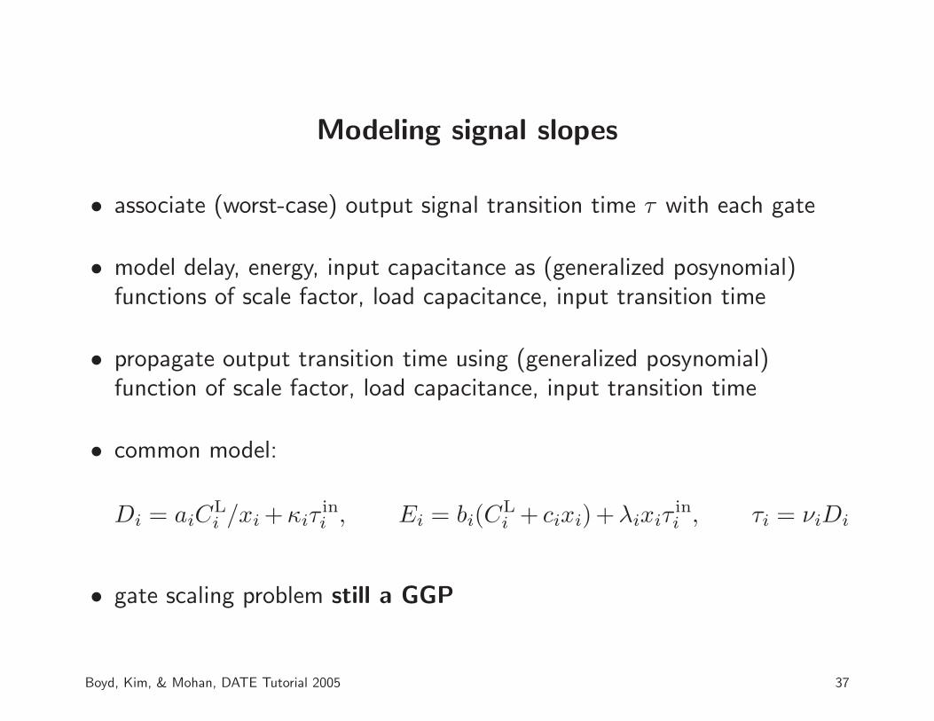
Modeling signal slopes
• associate (worst-case) output signal transition time τ with each gate
• model delay, energy, input capacitance as (generalized posynomial)functions of scale factor, load capacitance, input transition time
• propagate output transition time using (generalized posynomial)function of scale factor, load capacitance, input transition time
• common model:
Di = aiCLi /xi +κiτ
ini , Ei = bi(C
Li + cixi)+λixiτ
ini , τi = νiDi
• gate scaling problem still a GGP
Boyd, Kim, & Mohan, DATE Tutorial 2005 37

Design with a standard library
• circuit topology is fixed; choose size for each gate from discrete library
• a combinatorial optimization problem, difficult to solve exactly
• GP approach
– for each gate type in library, fit given library data to findGP-compatible models of delay, power, . . .
– size with continuous fitted models, using GP
– snap continuous scale factors back to standard library
Boyd, Kim, & Mohan, DATE Tutorial 2005 38

Robust design over corners
• have K corners or scenarios, e.g., combinations of
– process parameters (channel length, oxide thickness, . . . )– environmental parameters (supply voltage, temperature, . . . )
• for each corner have (slightly) different models for delay, power, . . .
• robust design finds gate scalings that work well for all corners
Boyd, Kim, & Mohan, DATE Tutorial 2005 39

Robust design over corners
• basic (worst-case) robust design over corners:
minimize Dwc = maxD(1), . . . , D(K)subject to P (1)(x) ≤ Pmax, . . . , P (K)(x) ≤ Pmax
A ≤ Amax
1 ≤ xi, i = 1, . . . , n
• many variations, e.g., minimize average delay over corners,
Davg = (1/K)(D(1) + · · · + D(K)
)
• results in (very large, but sparse) GGP
Boyd, Kim, & Mohan, DATE Tutorial 2005 40

Multiple-scenario design
• have K scenarios or operating modes, with K models for P , D, . . .
• scenarios are combinations of
– supply & threshold voltages– clock frequency– specifications & constraints
• like corner-based robust design, but scenarios are intentional
• find one set of gate scalings that work well in all scenarios
Boyd, Kim, & Mohan, DATE Tutorial 2005 41
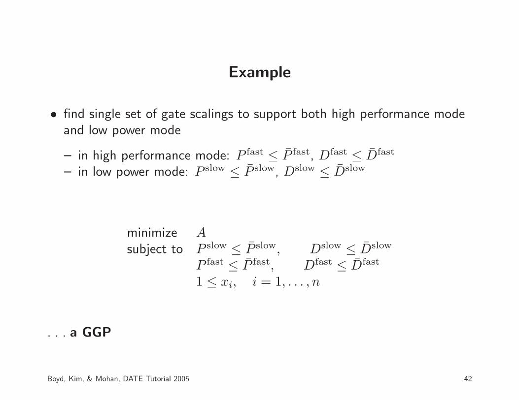
Example
• find single set of gate scalings to support both high performance modeand low power mode
– in high performance mode: P fast ≤ P fast, Dfast ≤ Dfast
– in low power mode: P slow ≤ P slow, Dslow ≤ Dslow
minimize Asubject to P slow ≤ P slow, Dslow ≤ Dslow
P fast ≤ P fast, Dfast ≤ Dfast
1 ≤ xi, i = 1, . . . , n
. . . a GGP
Boyd, Kim, & Mohan, DATE Tutorial 2005 42

Statistical parameter variation
• circuit peformance depends on random device and process parameters
• hence, performance measures like P , D are random variables P, D
• delay D is max of many random variables; often skewed to right
• distributions of P, D depend on gate scalings xi
45 53circuit delay
freq
uen
cy
• related to (parametric) yield, DFM, DFY . . .
Boyd, Kim, & Mohan, DATE Tutorial 2005 43
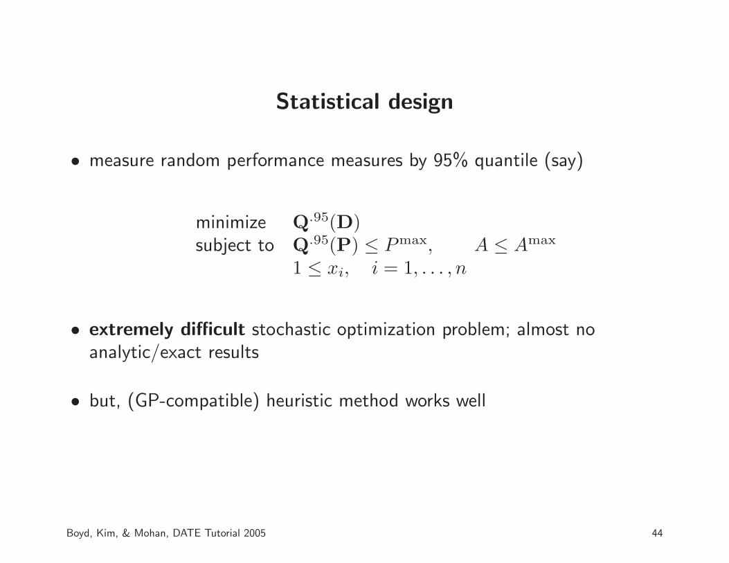
Statistical design
• measure random performance measures by 95% quantile (say)
minimize Q.95(D)subject to Q.95(P) ≤ Pmax, A ≤ Amax
1 ≤ xi, i = 1, . . . , n
• extremely difficult stochastic optimization problem; almost noanalytic/exact results
• but, (GP-compatible) heuristic method works well
Boyd, Kim, & Mohan, DATE Tutorial 2005 44

Statistical model
• for simplicity consider Vth variation only
• Pelgrom’s model: σVth= σVth
x−1/2
• alpha-power law model: D ∝ Vdd/(Vdd − Vth)α, with α ≈ 1.3
• for small variation in Vth,
σD ≈∣∣∣∣∂D
∂Vth
∣∣∣∣ σVth= α(Vdd − Vth)
−1σVthx−0.5D
• σD is posynomial
• get similar (posynomial) models for σD with more complex gate delaystatistical models
Boyd, Kim, & Mohan, DATE Tutorial 2005 45

Heuristic for statistical design
• assume generalized posynomial models for gate delay mean Di(x) andvariance σi(x)2
• optimize using surrogate gate delays
Di(x) = Di(x) + κiσi(x)
κiσi(x) are margins on gate delays (κi is typically 2 or 3)
• verify statistical performance via Monte Carlo analysis(can update κi’s and repeat)
Boyd, Kim, & Mohan, DATE Tutorial 2005 46

Heuristic for statistical design
heuristic statistical design
• often far superior to design obtained ignoring statistical variation
• not very sensitive to details of process variation statistics (distributionshape, correlations, . . . )
• below: 32-bit Ladner-Fisher adder, Pelgrom variance model
45 53circuit delay
freq
uen
cy
statistical design
nominal optimal design
Boyd, Kim, & Mohan, DATE Tutorial 2005 47

Path delay mean/std. dev. scatter plots
mean path delay
mean path delay
pat
hdel
ayst
d.dev
.pat
hdel
ayst
d.dev
.
10
10
50
50
0
0
3
3nominal optimal design
statistical design
Boyd, Kim, & Mohan, DATE Tutorial 2005 48
Joint size and supply/threshold voltage optimization
• goal: jointly optimize gate size, supply and threshold voltages via GGP
• need to: model delay, power as generalized posynomial functions ofgate size, supply and threshold voltages
Boyd, Kim, & Mohan, DATE Tutorial 2005 49

Generalized posynomial delay model
• alpha-power law model predicts variation in gate delay with Vdd, Vth:
Di =Vdd,i
(Vdd,i − Vth,i)αDi(x)
Di is generalized posynomial gate delay model, function of scalings x
• generalized posynomial approximation
Di = V 1−αdd,i (1 + Vth,i/Vdd,i + · · · + (Vth,i/Vdd,i)
5)αDi(x)
error under 1% for Vdd,i ≥ 2Vth,i, 1.3 ≤ α ≤ 2
Boyd, Kim, & Mohan, DATE Tutorial 2005 50

Generalized posynomial power model
• gate dynamic power: Pdyn =n∑
i=1
fi(CLi + C int
i )V 2dd,i
• simple static power model:
Pstat =
n∑
i=1
xiIleaki Vdd,i, I leak
i ∝ e−(Vth,i−γVdd,i)/V0
γ, V0 are (process) constants
• Pstat (by itself) cannot be approximated well by a generalizedposynomial over large range of Vdd, Vth
• but, total power P = Pdyn + Pstat can be approximated well by ageneralized posynomial
Boyd, Kim, & Mohan, DATE Tutorial 2005 51

Generalized posynomial power model example
total power P = V 2dd + 30Vdde
−(Vth−0.06Vdd)/0.039 (up to scaling)
VddVth
P
1
2
0.2
0.4
1
12
VddVth 1
2
0.2
0.4
1
12
|P−
b P|
• generalized posynomial approximationP = V 2
dd + 0.06Vdd(1 + 0.0031Vdd)500(Vth/0.039)−6.16
• error under 3% (well under accuracy of model!)
Boyd, Kim, & Mohan, DATE Tutorial 2005 52

Joint optimization of gate sizes, Vdd, & Vth
basic problem, with variables: xi, Vth,i, Vdd,i
minimize Dsubject to P ≤ Pmax, A ≤ Amax
V minth ≤ Vth,i ≤ V max
th , i = 1, . . . , nV min
dd ≤ Vdd,i ≤ V maxdd , i = 1, . . . , n
other constraints . . .
(. . . a GGP)
discrete allowed Vdd, Vth values yields MIGP
Boyd, Kim, & Mohan, DATE Tutorial 2005 53
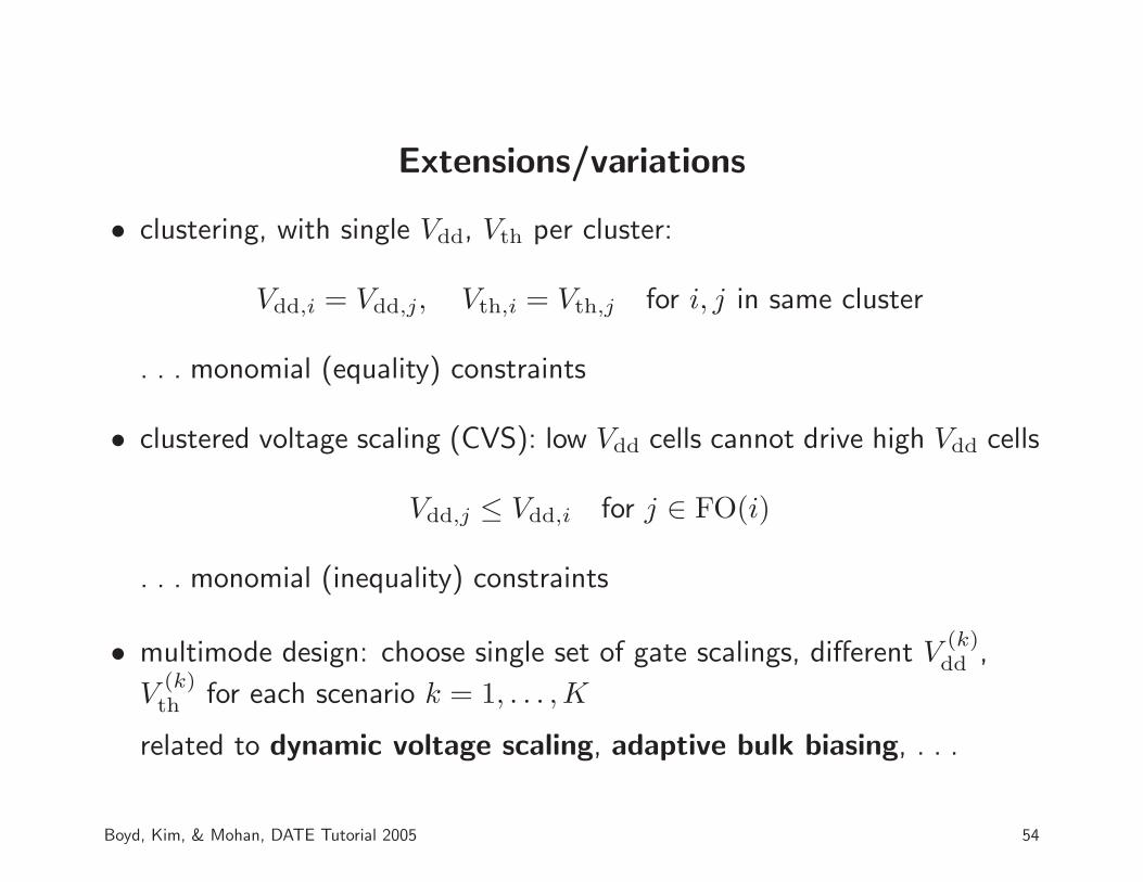
Extensions/variations
• clustering, with single Vdd, Vth per cluster:
Vdd,i = Vdd,j, Vth,i = Vth,j for i, j in same cluster
. . . monomial (equality) constraints
• clustered voltage scaling (CVS): low Vdd cells cannot drive high Vdd cells
Vdd,j ≤ Vdd,i for j ∈ FO(i)
. . . monomial (inequality) constraints
• multimode design: choose single set of gate scalings, different V(k)dd ,
V(k)th for each scenario k = 1, . . . ,K
related to dynamic voltage scaling, adaptive bulk biasing, . . .
Boyd, Kim, & Mohan, DATE Tutorial 2005 54

Joint optimization examples
• Ladner-Fisher adder
• variables: gate scalings xi, supply voltages Vdd,i, threshold voltages Vth,i
• four delay-power trade-off curves:
– fixed Vdd,i = 1.0, fixed Vth,i = 0.3
– fixed Vdd,i = 1.0, variable Vth,i ∈ 0.2, 0.3, 0.4– CVS with Vdd,i ∈ 0.6, 1.0, Vth,i ∈ 0.2, 0.3, 0.4– variable continuous Vdd, Vth, 0.6 ≤ Vdd,i ≤ 1.0, 0.2 ≤ Vth,i ≤ 0.4
(not practical, but serves as lower bound)
Boyd, Kim, & Mohan, DATE Tutorial 2005 55

Trade-off curve analysis
Dmax
P
37.5 750
30
lower bound
CVS
fixed Vdd, variable Vth
fixed Vdd, Vth
Boyd, Kim, & Mohan, DATE Tutorial 2005 56
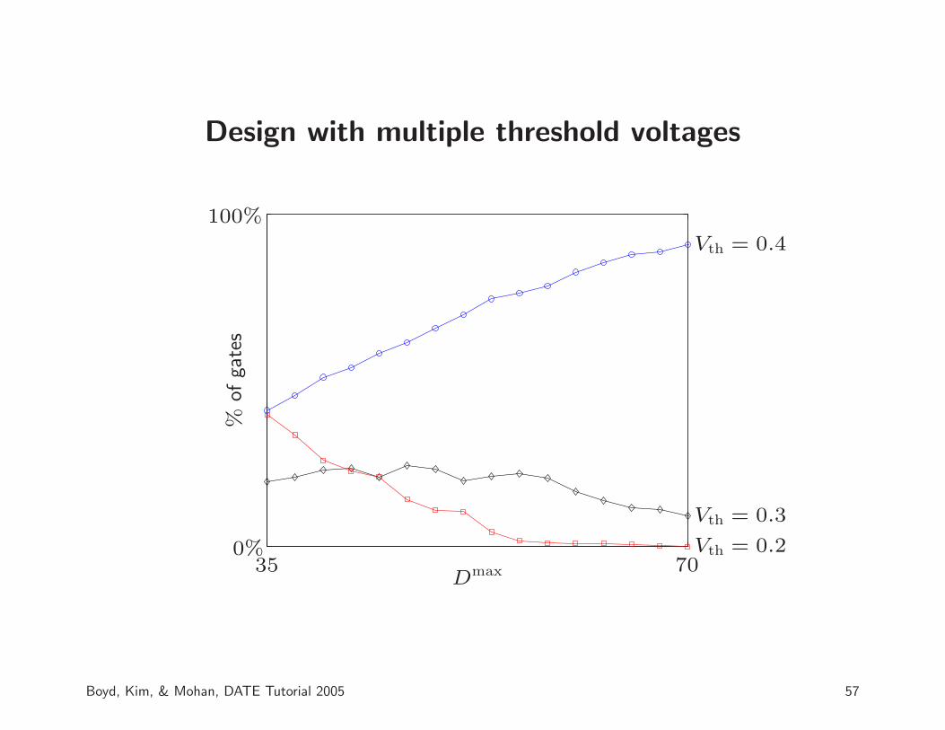
Design with multiple threshold voltages
Dmax
%of
gate
s
35 700%
100%
Vth = 0.4
Vth = 0.3
Vth = 0.2
Boyd, Kim, & Mohan, DATE Tutorial 2005 57

Clustered voltage scaling
%of
gate
s
37.5 750%
100% Vdd = 0.6
Vdd = 1.0
Boyd, Kim, & Mohan, DATE Tutorial 2005 58

Wire and device sizing
RC tree:
R1
R2 R3
R4
R5
R6
C1
C2 C3
C4 C6
C5
• Ris and Cis are generalized posynomials of some underlying variables x
Boyd, Kim, & Mohan, DATE Tutorial 2005 59

Elmore delay
• Elmore delay at node i:
Di =
∫ ∞
0
vi(t) dt
area under voltage curve, when voltages are initialized as vi(0) = 1
t
1 Di
• Elmore delay of RC tree is D = maxD1, . . . , DN
Boyd, Kim, & Mohan, DATE Tutorial 2005 60

Elmore delay expression
• analytic expression for Elmore delay Di
Di =∑
j∈P(i)
RiCtoti
• P(i) is path from root to node i
• Ctoti is the total capacitance downstream from node i (including Ci)
• Di is posynomial of x
• D is generalized posynomial of x
Boyd, Kim, & Mohan, DATE Tutorial 2005 61

RC tree optimization
• minimize RC tree delay subject to (generalized posynomial) constraints
minimize Dsubject to fi(x) ≤ 0, i = 1, . . . , m
. . . a GGP
• sparse formulation:
minimize ssubject to s ≥ Di, i = 1, . . . , n
Ctotj ≥
∑i∈Child(j) Ctot
i + Cj, i = 1, . . . , n
Di ≥ DPar(k) + RiCtoti , i = 1, . . . , n
fi(x) ≤ 0, i = 1, . . . ,m
Boyd, Kim, & Mohan, DATE Tutorial 2005 62

Wire sizing
• choose wire segment widths wi, . . . , wN in an interconnect network
• optimize delay, area
1
2 3
4 5
C1
C2 C3
C4 C5vin
Rs
Boyd, Kim, & Mohan, DATE Tutorial 2005 63

π model for wire segment
wi
li
Ci Ci
Ri
• wire resistance and capacitances
Ri = αiliwi
, Ci = βiliwi + γili,
• with π model, interconnect network becomes RC tree, with Ris and Cisposynomial functions of wire segment widths wi
Boyd, Kim, & Mohan, DATE Tutorial 2005 64
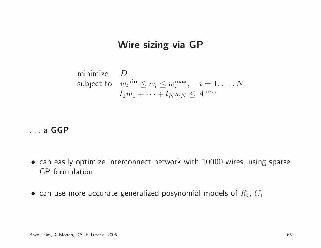
Wire sizing via GP
minimize Dsubject to wmin
i ≤ wi ≤ wmaxi , i = 1, . . . , N
l1w1 + · · · + lNwN ≤ Amax
. . . a GGP
• can easily optimize interconnect network with 10000 wires, using sparseGP formulation
• can use more accurate generalized posynomial models of Ri, Ci
Boyd, Kim, & Mohan, DATE Tutorial 2005 65

Device sizing
• devices (and wire segments) are sized individually
• replace each device with switch-level RC model
• each transition is associated with RC tree
• use Elmore delay to measure delay of transition
• . . . problem is GGP
Boyd, Kim, & Mohan, DATE Tutorial 2005 66
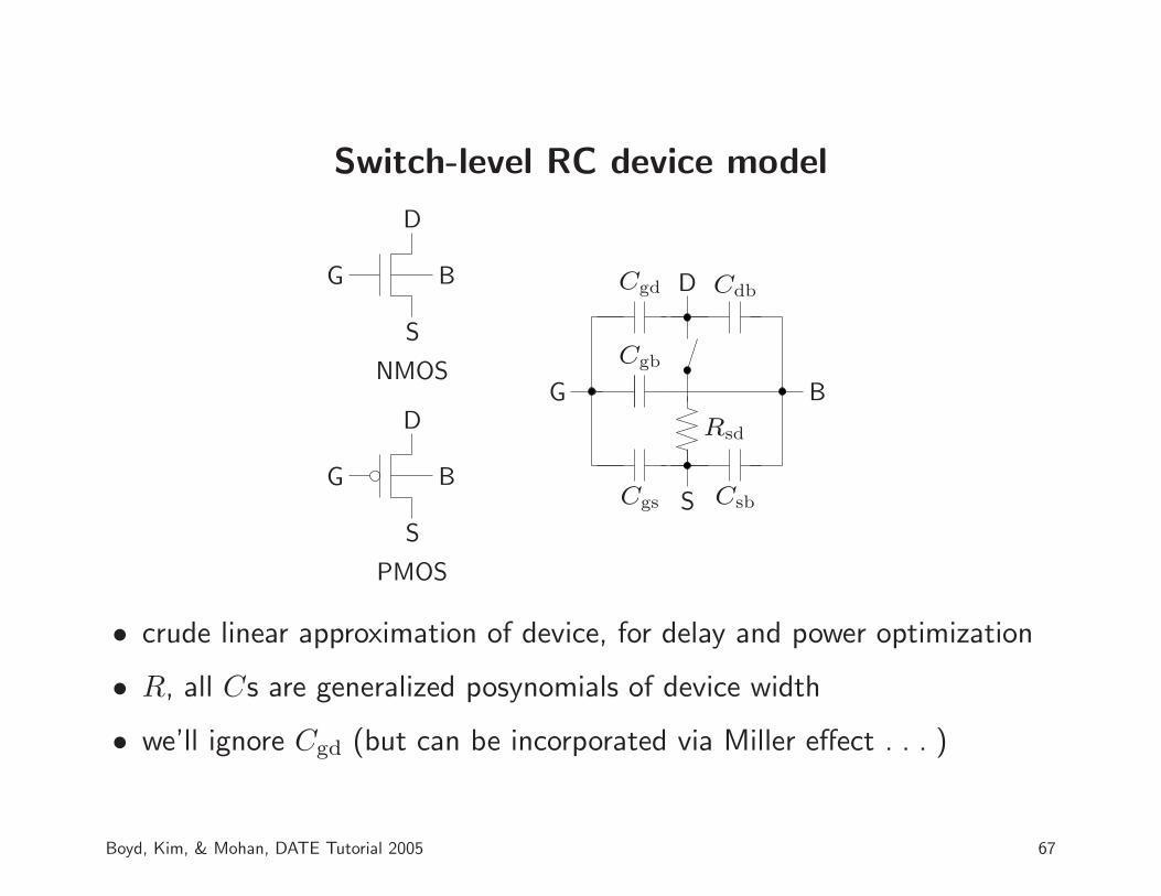
Switch-level RC device model
G
S
D
B
G
G
D
D
S
S
B
B
NMOS
PMOS
Rsd
Cgb
Cgd
Cgs
Cdb
Csb
• crude linear approximation of device, for delay and power optimization
• R, all Cs are generalized posynomials of device width
• we’ll ignore Cgd (but can be incorporated via Miller effect . . . )
Boyd, Kim, & Mohan, DATE Tutorial 2005 67
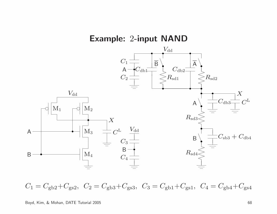
Example: 2-input NAND
A
B
M1 M2
M3
M4
X
CL
Vdd
Rsd1 Rsd2
Rsd3
Rsd4
C1
C2
C3
C4
B A
A
B
Cdb3
Csb3 + Cdb4
Cdb1 Cdb2A
B
X
CL
Vdd
Vdd
C1 = Cgb2+Cgs2, C2 = Cgb3+Cgs3, C3 = Cgb1+Cgs1, C4 = Cgb4+Cgs4
Boyd, Kim, & Mohan, DATE Tutorial 2005 68

Example transition
• transition: B falls from Vdd to zero; A remains at Vdd
• associated RC tree:
Rsd1
Rsd3C1
C2
CL
Vdd
C1 = Cdb1 + Cdb2 + Cdb3, C2 = Csb3 + Cdb4
• Elmore delay: D = Rsd1(CL + C1 + C2)
• energy lost: E = (CL + C1 + C2)V2dd/2
Boyd, Kim, & Mohan, DATE Tutorial 2005 69

Analog and RF Circuit Design Applications

Large signal MOS model
PMOSNMOS
D
D
G G
S
S
II
• gate overdrive voltage Vgov = Vgs − Vth
• saturation condition: Vds ≥ Vdsat = Vgov (Vdsat is minimumdrain-source voltage for device to operate in saturation)
• square-law model I = 0.5µCox(W/L)V 2gov
• GP model variables: I, L, W
• Vgov = (µCox/2)−1/2I1/2L1/2W−1/2 is monomial
• Vgs = Vgov + Vth is posynomial
Boyd, Kim, & Mohan, DATE Tutorial 2005 70

Small signal dynamic MOS model
PSfrag
Cgb Cgs gmvgs go Cdb
Cgd
B S
DG
• transconductance gm = (2µCox)1/2I1/2L−1/2W 1/2 is monomial
• output conductance go = λI is monomial
• all capacitances are (approximately) posynomial in I, L, W
• better (GP-compatible) models can be obtained by fitting data fromaccurate models or measurements
Boyd, Kim, & Mohan, DATE Tutorial 2005 71
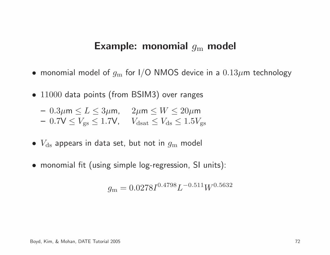
Example: monomial gm model
• monomial model of gm for I/O NMOS device in a 0.13µm technology
• 11000 data points (from BSIM3) over ranges
– 0.3µm ≤ L ≤ 3µm, 2µm ≤ W ≤ 20µm– 0.7V ≤ Vgs ≤ 1.7V, Vdsat ≤ Vds ≤ 1.5Vgs
• Vds appears in data set, but not in gm model
• monomial fit (using simple log-regression, SI units):
gm = 0.0278I0.4798L−0.511W 0.5632
Boyd, Kim, & Mohan, DATE Tutorial 2005 72

Example: monomial gm model
• fitting (relative) error cumulative distribution plot:
fitting error
frac
tion
ofdat
apoi
nts
0% 5% 10%0%
100%
• for 90% of points, fit is better than 4%
Boyd, Kim, & Mohan, DATE Tutorial 2005 73
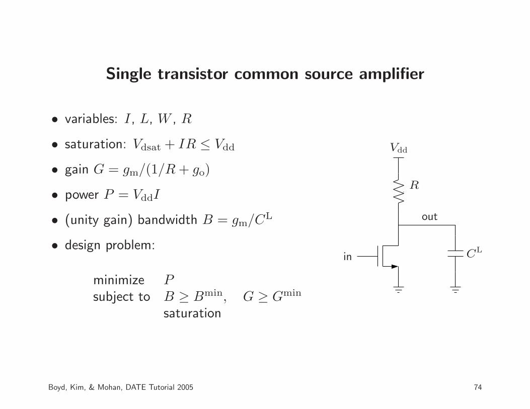
Single transistor common source amplifier
• variables: I, L, W , R
• saturation: Vdsat + IR ≤ Vdd
• gain G = gm/(1/R + go)
• power P = VddI
• (unity gain) bandwidth B = gm/CL
• design problem:
minimize Psubject to B ≥ Bmin, G ≥ Gmin
saturation
CL
R
Vdd
in
out
Boyd, Kim, & Mohan, DATE Tutorial 2005 74
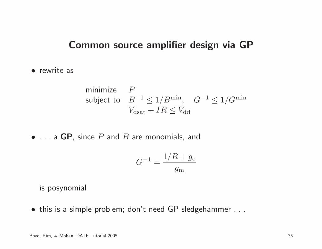
Common source amplifier design via GP
• rewrite as
minimize Psubject to B−1 ≤ 1/Bmin, G−1 ≤ 1/Gmin
Vdsat + IR ≤ Vdd
• . . . a GP, since P and B are monomials, and
G−1 =1/R + go
gm
is posynomial
• this is a simple problem; don’t need GP sledgehammer . . .
Boyd, Kim, & Mohan, DATE Tutorial 2005 75

Current mirror opamp
M1
M3
M5
M6
M7
M2
M4
M8
M9
M10
CL
Iref
Vdd
in+in−
out
• M1,M2 and M3,M4 matched pairs
• four current mirrors: M8,M5; M10,M7; M9,M3; M4, M6
Boyd, Kim, & Mohan, DATE Tutorial 2005 76
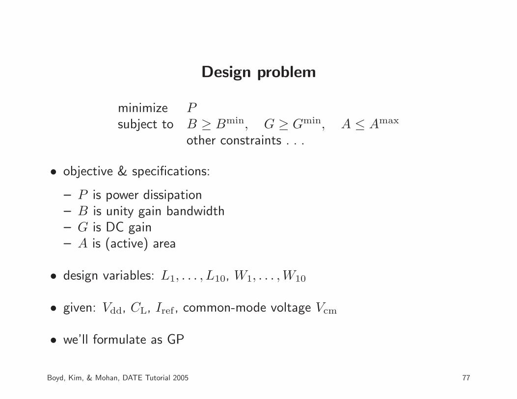
Design problem
minimize Psubject to B ≥ Bmin, G ≥ Gmin, A ≤ Amax
other constraints . . .
• objective & specifications:
– P is power dissipation– B is unity gain bandwidth– G is DC gain– A is (active) area
• design variables: L1, . . . , L10, W1, . . . ,W10
• given: Vdd, CL, Iref, common-mode voltage Vcm
• we’ll formulate as GP
Boyd, Kim, & Mohan, DATE Tutorial 2005 77
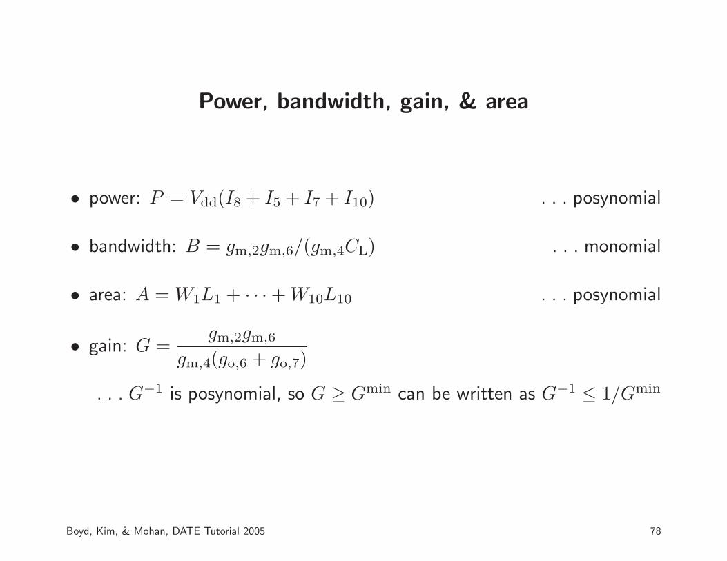
Power, bandwidth, gain, & area
• power: P = Vdd(I8 + I5 + I7 + I10) . . . posynomial
• bandwidth: B = gm,2gm,6/(gm,4CL) . . . monomial
• area: A = W1L1 + · · · + W10L10 . . . posynomial
• gain: G =gm,2gm,6
gm,4(go,6 + go,7)
. . . G−1 is posynomial, so G ≥ Gmin can be written as G−1 ≤ 1/Gmin
Boyd, Kim, & Mohan, DATE Tutorial 2005 78

Dimension, matching, and current constraints
• limits on device sizes: Lmin ≤ Li ≤ Lmax, Wmin ≤ Wi, i = 1, . . . , 10
• differential symmetry constraints (M1, M2 and M3, M4 matched):
W1 = W2, L1 = L2, I1 = I2,W3 = W4, L3 = L4, I3 = I4,
• length & gate overdrive voltage matched for current mirror pairs:
L5 = L8, L10 = L7, L3 = L9, L4 = L6
Vgov,5 = Vgov,8, Vgov,10 = Vgov,7, Vgov,3 = Vgov,9, Vgov,4 = Vgov,6
• current relations:
I1 = I3 = I5/2, I8 = Iref, I6 = I7, I9 = I10
Boyd, Kim, & Mohan, DATE Tutorial 2005 79

Saturation constraints
• diode connected devices (M3,M4,M8, M10) automatically in saturation
• others must have Vds ≥ Vdsat:
– M7: Vdsat,7 ≤ Vcm
– M6: Vdsat,6 + Vcm ≤ Vdd
– M9: Vdsat,9 + Vgs,10 ≤ Vdd
– M5: Vds,5 + Vgs,1 ≤ Vcm
– M1 & M2: Vcm + Vgs,3 ≤ Vdd + Vth
• . . . all are posynomial inequalities
Boyd, Kim, & Mohan, DATE Tutorial 2005 80

Node capacitances and non-dominant poles
• capacitances at nodes are posynomials, e.g.,
Cout = Cgd,6 + Cdb,6 + Cgd,7 + Cdb,7 + CL
• non-dominant time constants are posynomials:
τ1 =Cd1
gm,3, τ2 =
Cd2
gm,4, τ9 =
Cd9
gm,10
(Cd1, Cd2, Cd9 are node capacitances at drains of M1,M2,M9)
• to limit effect of non-dominant poles, make sum smaller than dominanttime constant:
τ1 + τ2 + τ9 ≤ τdom = CL/gm
. . . a posynomial constraint
Boyd, Kim, & Mohan, DATE Tutorial 2005 81

Power versus bandwidth trade-off
10 6010
−1
100
101
Gmin = 10
Gmin = 20
Gmin = 30
Bmin (MHz)
P(m
W)
Boyd, Kim, & Mohan, DATE Tutorial 2005 82

Joint electrical/physical design
• each device has a (physical) cell width w and height h for floor planning
• devices are folded into multiple fingers
• (approximate) posynomial or monomial relations link electrical variables(I, L, W ) and physical variables (w, h), e.g.,
– cell area is at least 4× active area: wh ≥ 4WL– cell aspect ratio limited to 5:1: 1/5 ≤ w/h ≤ 5
W/6
L
w
h
Boyd, Kim, & Mohan, DATE Tutorial 2005 83

Slicing tree layout scheme
• vertical and horizontal slices fix relative placement of device cells
• leaves are device cells; root is bounding box
v
h h
M1
vM4 M5
M2 M3
M1
M4
M2 M3
M5
wbbox
hbbox
Boyd, Kim, & Mohan, DATE Tutorial 2005 84
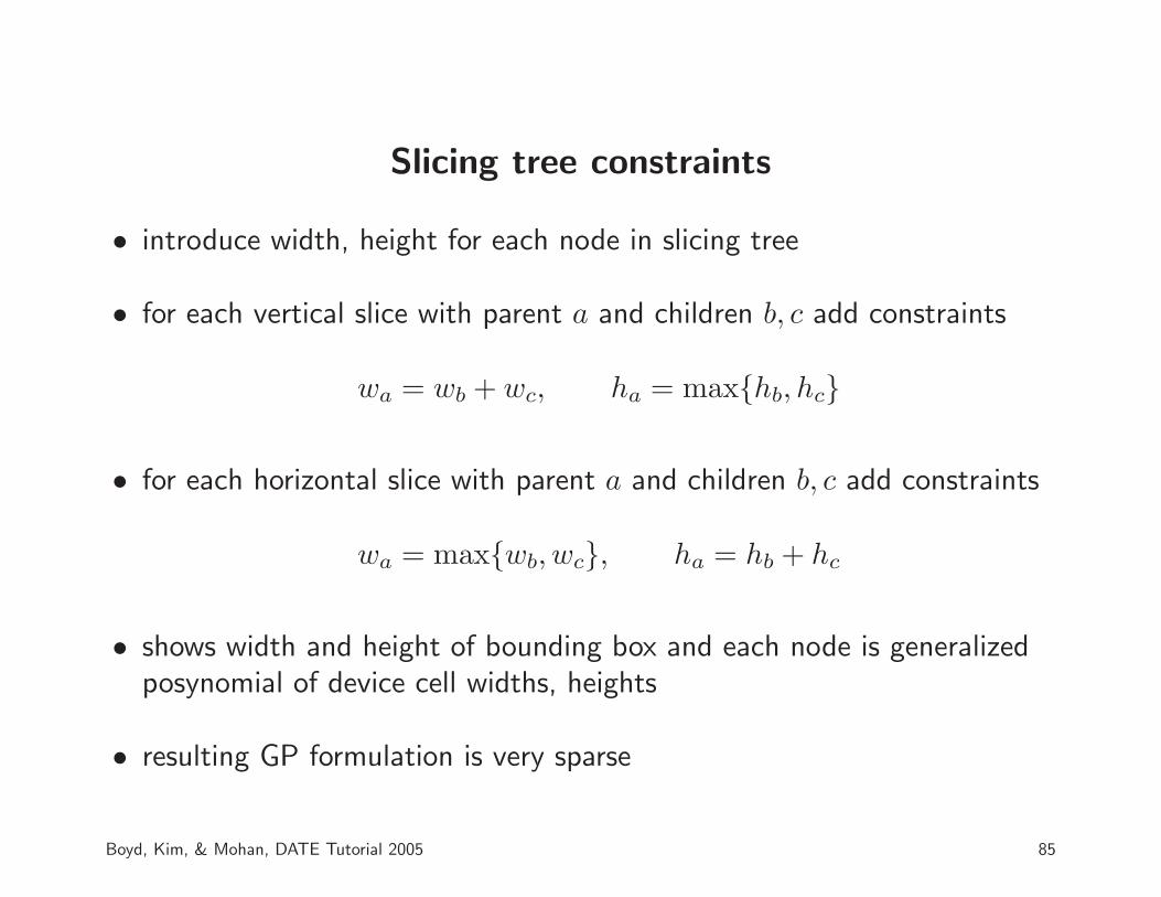
Slicing tree constraints
• introduce width, height for each node in slicing tree
• for each vertical slice with parent a and children b, c add constraints
wa = wb + wc, ha = maxhb, hc
• for each horizontal slice with parent a and children b, c add constraints
wa = maxwb, wc, ha = hb + hc
• shows width and height of bounding box and each node is generalizedposynomial of device cell widths, heights
• resulting GP formulation is very sparse
Boyd, Kim, & Mohan, DATE Tutorial 2005 85

Joint electrical/physical design via GP
• form one GP that includes
– electrical variables, constraints (Ii, Li, Wi, gm,i . . .)– physical variables, constraints (wi, hi, w
bbox, hbbox, . . .)– coupling constraints (wihi ≥ 4WiLi, . . . )
• solve it all together
• extensions: can add
– parasitic estimates– more accurate expressions for device cell dimensions– channels for routing
Boyd, Kim, & Mohan, DATE Tutorial 2005 86

Optimal filter implementation
simple Gm-C two-pole lowpass filter
g1g2
C1 C2
inputoutput
transfer function is
H(s) =1
1 + t1s + t1t2s2, t1 = C1/g1, t2 = C2/g2
gi is amplifier transconductance
Boyd, Kim, & Mohan, DATE Tutorial 2005 87

Noise analysis
• Ni is input referred (white) amplifier input-referred voltage density
• spectral density of output noise is
N(ω)2 =N2
1 + ω2N22
(1 − t1t2ω2)2 + t21ω2
• root-mean-square output noise voltage is
M =
(∫ ∞
0
N(ω)2 dω
)1/2
=(αN2
1 + βN22
)1/2
Boyd, Kim, & Mohan, DATE Tutorial 2005 88
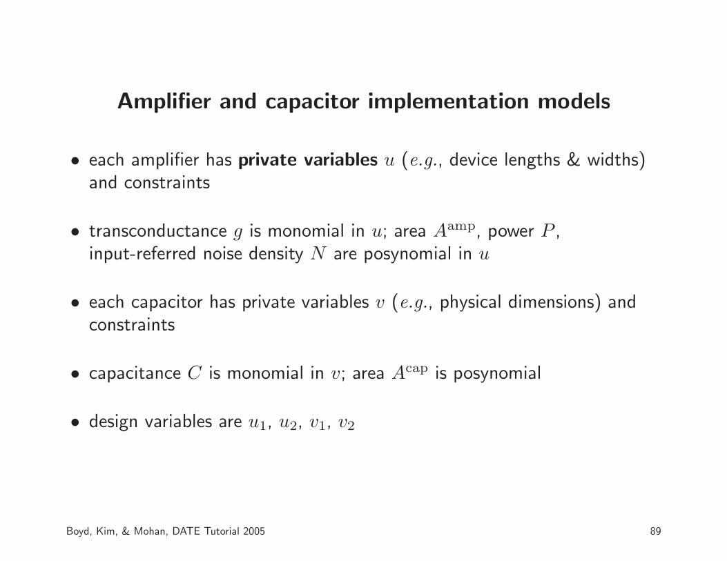
Amplifier and capacitor implementation models
• each amplifier has private variables u (e.g., device lengths & widths)and constraints
• transconductance g is monomial in u; area Aamp, power P ,input-referred noise density N are posynomial in u
• each capacitor has private variables v (e.g., physical dimensions) andconstraints
• capacitance C is monomial in v; area Acap is posynomial
• design variables are u1, u2, v1, v2
Boyd, Kim, & Mohan, DATE Tutorial 2005 89

Optimal filter implementation problem
• filter is Butterworth with frequency ωc:
t1 =√
2/ωc, t2 = (1/√
2)/ωc
• minimize total power of implementation, subject to area, output noiselimits:
minimize P (u1) + P (u2)
subject to t1 =√
2/ωc, t2 = (1/√
2)/ωc
Aamp(u1) + Aamp(u2) + Acap(v1) + Acap(v2) ≤ Amax
M = (ωc/4√
2)(N21 + 2N2
2 )1/2 ≤ Mmax
• a GGP in the variables u1, u2, v1, v2
Boyd, Kim, & Mohan, DATE Tutorial 2005 90

Example
• Butterworth filter with ωc = 108rad/s
• private variables in amplifiers: (equivalent) L, W
• amplifier model:
Aamp = WL, P = 2.5·10−4W/L,
g = 4·10−5W/L, N =√
7.5·10−16L/W
(based on simple model with Vdd = 2.5, Vgov = 0.2)
• private variable in capacitors is area Acap; C = 10−4Acap
• Amax = 4·10−6
Boyd, Kim, & Mohan, DATE Tutorial 2005 91
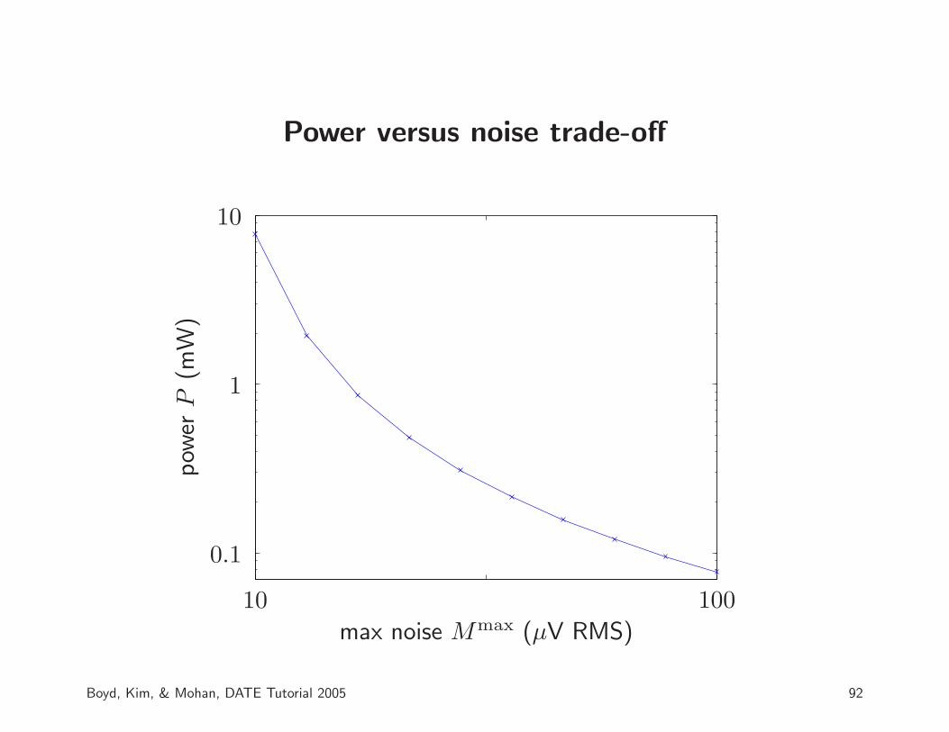
Power versus noise trade-off
pow
erP
(mW
)
max noise Mmax (µV RMS)
10 100
0.1
1
10
Boyd, Kim, & Mohan, DATE Tutorial 2005 92

Spiral inductor/differential resonator optimization
planar loop
inductor−v/2 +v/2
RL
CL
• loop inductor connected to (given) RL and CL
• differential (floating) mode operation
• inductor designed to resonate at operating frequency f
Boyd, Kim, & Mohan, DATE Tutorial 2005 93

Design problem: differential resonator
maximize RT
subject to QT ≥ QminT , A ≤ Amax
other constraints . . .
• objective & specifications:
– RT is tank impedance (which is real at operating frequency f)– QT is tank quality factor– A is area of loop inductor
• design variables: dimensions of loop inductor
• load resistance RL, load capacitance CL, frequency f given
• we’ll formulate as GP
Boyd, Kim, & Mohan, DATE Tutorial 2005 94

Loop inductor
W
D
• (centerline) diameter D
• width W
• outer diameter is D + W ; area is A = (D + W )2
Boyd, Kim, & Mohan, DATE Tutorial 2005 95
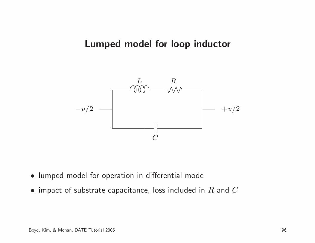
Lumped model for loop inductor
L R
C
−v/2 +v/2
• lumped model for operation in differential mode
• impact of substrate capacitance, loss included in R and C
Boyd, Kim, & Mohan, DATE Tutorial 2005 96

Example
• frequency range 2GHz ≤ f ≤ 6GHz
• metal layer thickness 2µm, resistivity 5·10−8Ωm
• metal-substrate capacitance density 5·10−6Fm2
• width, diameter constraints:
150µm ≤ D ≤ 600µm, 4µm ≤ W ≤ 30µm, 10 ≤ D/W ≤ 100
Boyd, Kim, & Mohan, DATE Tutorial 2005 97

GP models for L, R and C
• can get exact values via EM simulation
• inductance (monomial)
L = 2.1·10−6D1.28W−0.25f−0.01
• resistance (posynomial)
R = 0.1DW−1+3·10−6DW−0.84f0.5+5·10−9DW−0.76f0.75+0.02DWf
• capacitance (posynomial):
C = 5·10−6DW + 1·10−11D
Boyd, Kim, & Mohan, DATE Tutorial 2005 98
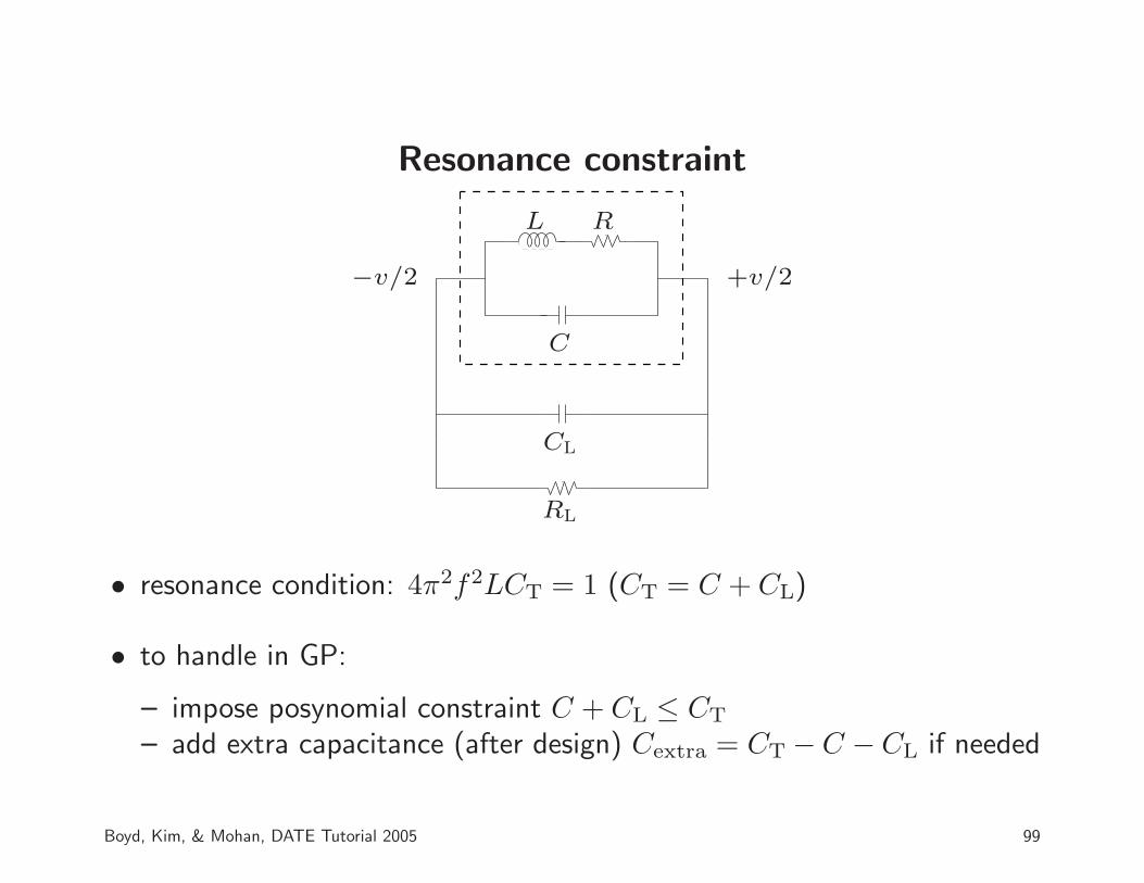
Resonance constraint
L R
C
RL
CL
−v/2 +v/2
• resonance condition: 4π2f2LCT = 1 (CT = C + CL)
• to handle in GP:
– impose posynomial constraint C + CL ≤ CT
– add extra capacitance (after design) Cextra = CT − C − CL if needed
Boyd, Kim, & Mohan, DATE Tutorial 2005 99

Tank conductance and quality factor
L R
C
RL
CL
−v/2 +v/2
• tank conductance: GT =1
RT=
R
4π2f2L2+
1
RL. . . posynomial
• inverse of tank quality factor:1
QT=
R
2πfL+
2πfL
RL. . . posynomial
Boyd, Kim, & Mohan, DATE Tutorial 2005 100

Reso
nance
impedance
vers
us
area
trade-o
ff
RT(Ω)
Am
ax
(mm
2)
100
300
500 0.0
50.1
50.
25CL
=0.
6pF
CL
=0.
8pF
CL
=1.
0pF
Boy
d,K
im,&
Moh
an,D
AT
ETuto
rial
2005
101

LC oscillator
loopinductor
−v/2 +v/2
Vdd
Ibias
CL CL
...
VcCv Cv
2B−1Csw
Csw
• loop inductor
• varactors for fine tuning
• binary weighted switchingcapacitors for coarse tuning
• cross coupled NMOStransistors
• tail current source
Boyd, Kim, & Mohan, DATE Tutorial 2005 102
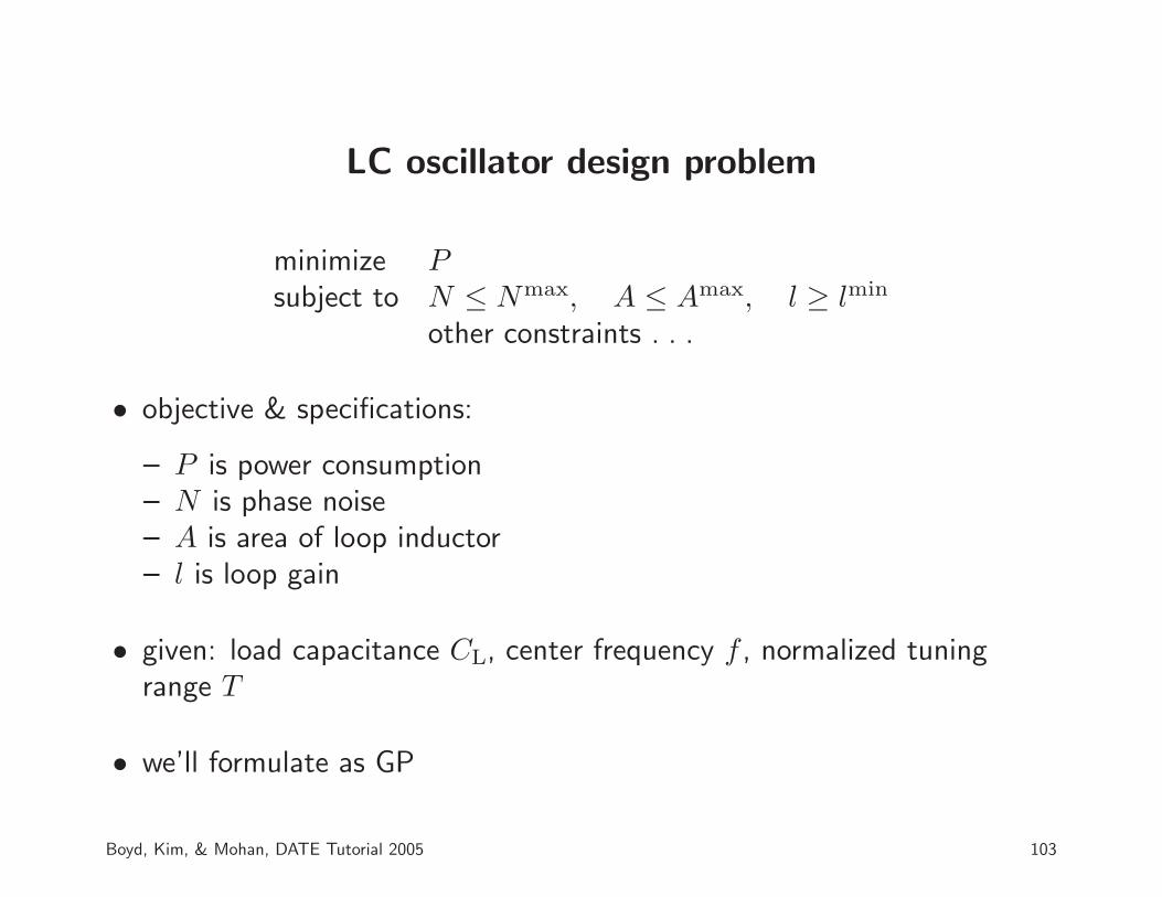
LC oscillator design problem
minimize Psubject to N ≤ Nmax, A ≤ Amax, l ≥ lmin
other constraints . . .
• objective & specifications:
– P is power consumption– N is phase noise– A is area of loop inductor– l is loop gain
• given: load capacitance CL, center frequency f , normalized tuningrange T
• we’ll formulate as GP
Boyd, Kim, & Mohan, DATE Tutorial 2005 103
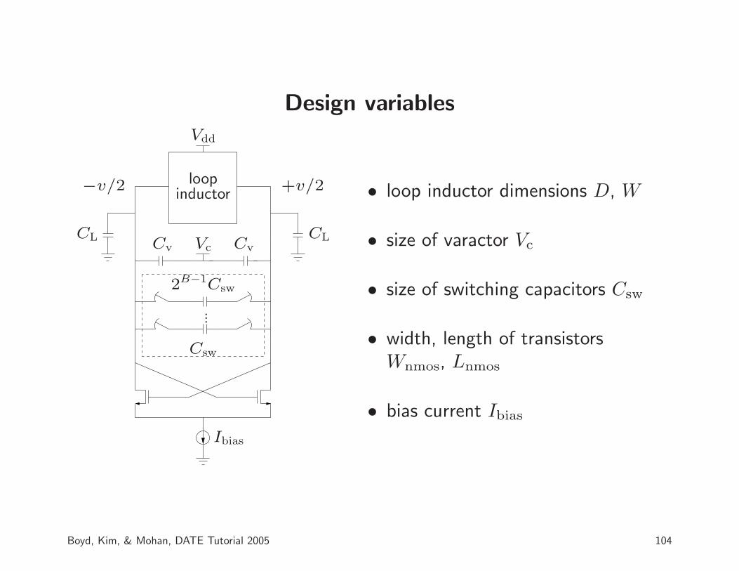
Design variables
loopinductor
−v/2 +v/2
Vdd
Ibias
CL CL
...
VcCv Cv
2B−1Csw
Csw
• loop inductor dimensions D, W
• size of varactor Vc
• size of switching capacitors Csw
• width, length of transistorsWnmos, Lnmos
• bias current Ibias
Boyd, Kim, & Mohan, DATE Tutorial 2005 104

Current source, switched capacitor, and varactor models
• Ibias is bias current, with minimum operating voltage Vbias
• binary weighted capacitors
– B is number of bits for switching capacitors– Csw is LSB switching capacitance; 2B−1Csw is MSB switching
capacitance
• varactor
– Cv is minimum varactor capacitance; KvCv is maximum(Kv is process constant)
– varactor range covers 2 LSB: 2Csw ≤ 0.5(Kv − 1)Cv
Boyd, Kim, & Mohan, DATE Tutorial 2005 105
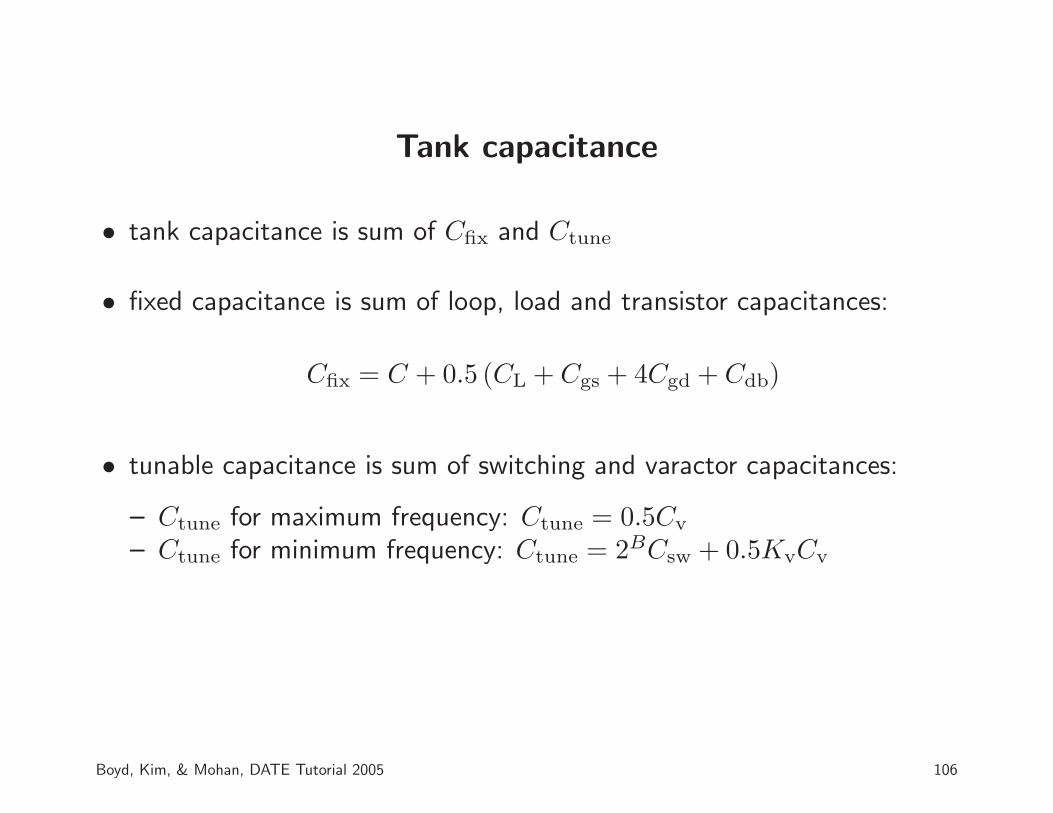
Tank capacitance
• tank capacitance is sum of Cfix and Ctune
• fixed capacitance is sum of loop, load and transistor capacitances:
Cfix = C + 0.5 (CL + Cgs + 4Cgd + Cdb)
• tunable capacitance is sum of switching and varactor capacitances:
– Ctune for maximum frequency: Ctune = 0.5Cv
– Ctune for minimum frequency: Ctune = 2BCsw + 0.5KvCv
Boyd, Kim, & Mohan, DATE Tutorial 2005 106

Resonance frequency & tuning
• capacitance constraint at maximum frequency: Cfix + 0.5Cv ≤ Cf,max
• maximum frequency: (2πf(1 + T ))2LCf,max = 1
• capacitance at center frequency: (2πf)2LCf,c = 1
• tuning range constraint:
4T
(1 − T 2)2Cf,c ≤ Csw
(2B + 2
)
Boyd, Kim, & Mohan, DATE Tutorial 2005 107
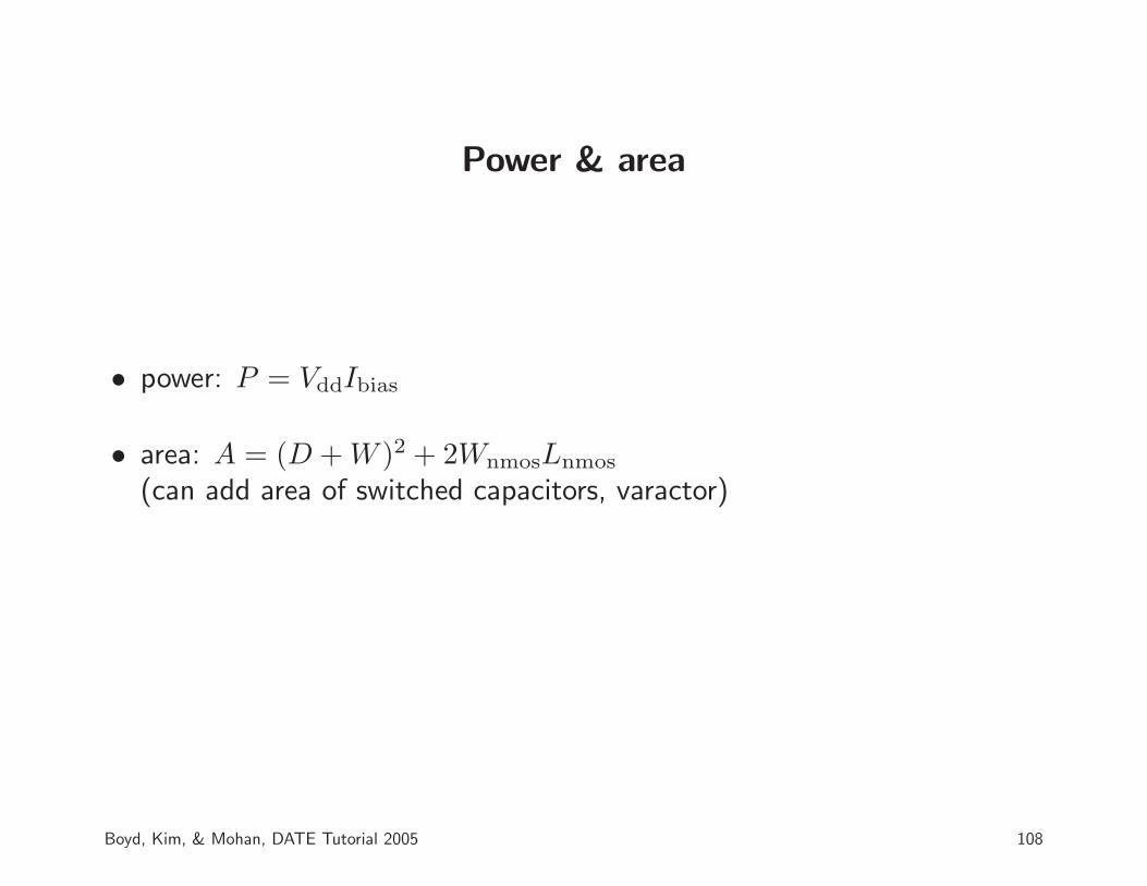
Power & area
• power: P = VddIbias
• area: A = (D + W )2 + 2WnmosLnmos
(can add area of switched capacitors, varactor)
Boyd, Kim, & Mohan, DATE Tutorial 2005 108

Tank conductance & voltage swing
• tank conductance is posynomial: GT =R
4π2f2L2+ 0.5go
• differential voltage amplitude: Vosc + 2Vbias ≤ 2Vdd, VoscGT ≤ Ibias
Boyd, Kim, & Mohan, DATE Tutorial 2005 109
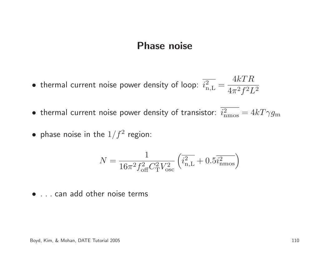
Phase noise
• thermal current noise power density of loop: i2n,L =4kTR
4π2f2L2
• thermal current noise power density of transistor: i2nmos = 4kTγgm
• phase noise in the 1/f2 region:
N =1
16π2f2offC2
TV 2osc
(i2n,L + 0.5i2nmos
)
• . . . can add other noise terms
Boyd, Kim, & Mohan, DATE Tutorial 2005 110
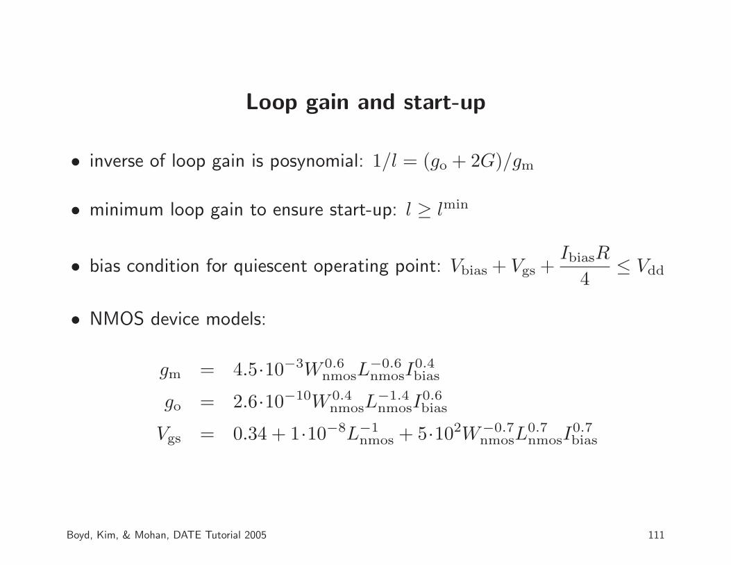
Loop gain and start-up
• inverse of loop gain is posynomial: 1/l = (go + 2G)/gm
• minimum loop gain to ensure start-up: l ≥ lmin
• bias condition for quiescent operating point: Vbias + Vgs +IbiasR
4≤ Vdd
• NMOS device models:
gm = 4.5·10−3W 0.6nmosL
−0.6nmosI
0.4bias
go = 2.6·10−10W 0.4nmosL
−1.4nmosI
0.6bias
Vgs = 0.34 + 1·10−8L−1nmos + 5·102W−0.7
nmosL0.7nmosI
0.7bias
Boyd, Kim, & Mohan, DATE Tutorial 2005 111
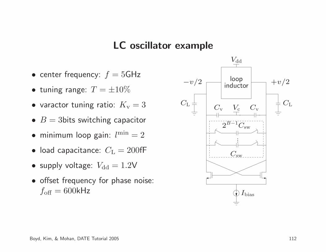
LC oscillator example
• center frequency: f = 5GHz
• tuning range: T = ±10%
• varactor tuning ratio: Kv = 3
• B = 3bits switching capacitor
• minimum loop gain: lmin = 2
• load capacitance: CL = 200fF
• supply voltage: Vdd = 1.2V
• offset frequency for phase noise:foff = 600kHz
loopinductor
−v/2 +v/2
Vdd
Ibias
CL CL
...
VcCv Cv
2B−1Csw
Csw
Boyd, Kim, & Mohan, DATE Tutorial 2005 112
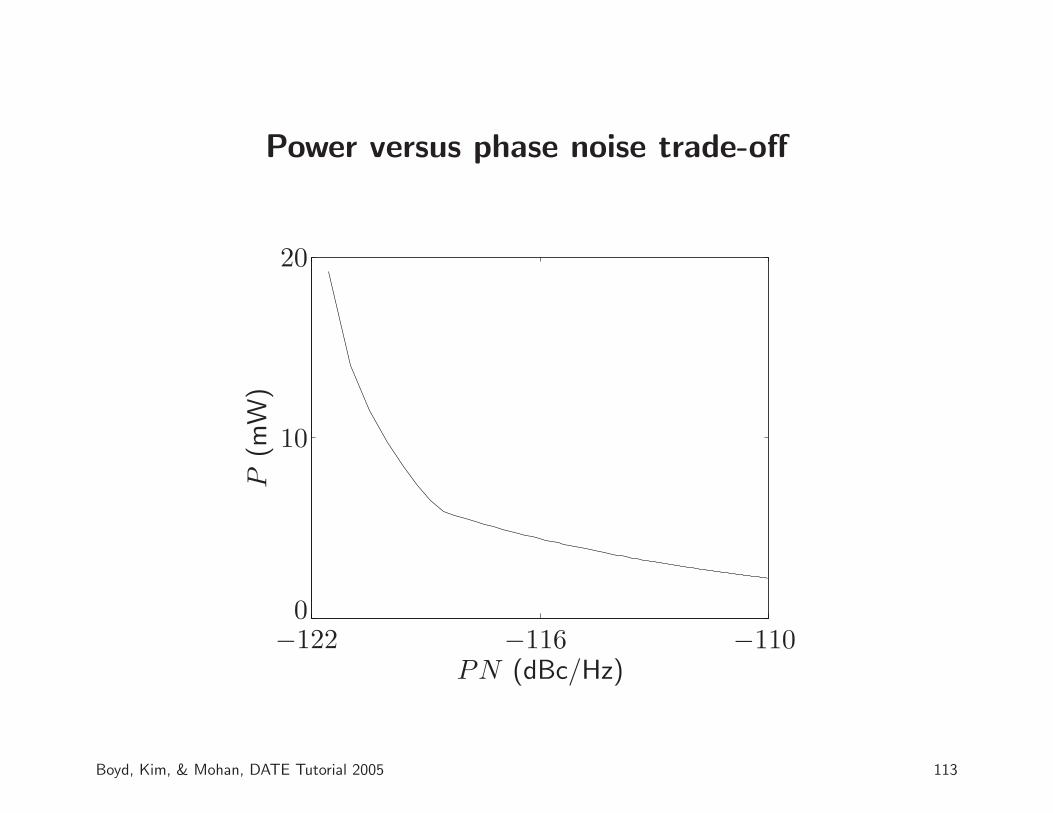
Power versus phase noise trade-off
P(m
W)
PN (dBc/Hz)
0
10
20
−122 −116 −110
Boyd, Kim, & Mohan, DATE Tutorial 2005 113

Monomial and Posynomial Fitting

A basic property of posynomials
• if f is a monomial, then log f(ey) is affine (linear plus constant)
• if f is a posynomial, then log f(ey) is convex
• roughly speaking, a posynomial is convex when plotted on log-log plot
• midpoint rule for posynomial f :
– let z be elementwise geometric mean of x, y, i.e., zi =√
xiyi
– then f(z) ≤√
f(x)f(y)
• a converse: if log φ(ey) is convex, then φ can be approximated as wellas you like by a posynomial
Boyd, Kim, & Mohan, DATE Tutorial 2005 114
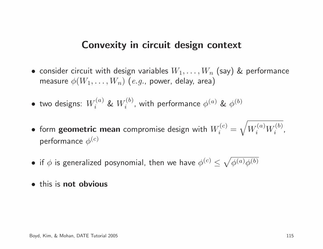
Convexity in circuit design context
• consider circuit with design variables W1, . . . , Wn (say) & performancemeasure φ(W1, . . . , Wn) (e.g., power, delay, area)
• two designs: W(a)i & W
(b)i , with performance φ(a) & φ(b)
• form geometric mean compromise design with W(c)i =
√W
(a)i W
(b)i ,
performance φ(c)
• if φ is generalized posynomial, then we have φ(c) ≤√
φ(a)φ(b)
• this is not obvious
Boyd, Kim, & Mohan, DATE Tutorial 2005 115
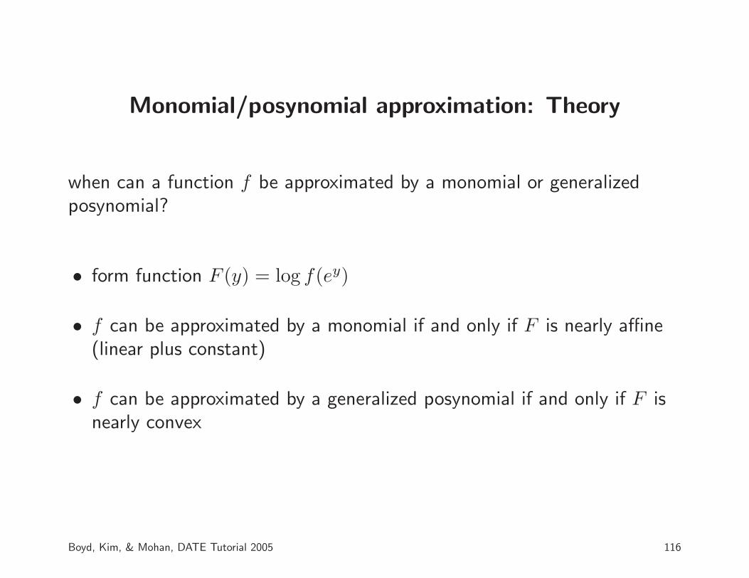
Monomial/posynomial approximation: Theory
when can a function f be approximated by a monomial or generalizedposynomial?
• form function F (y) = log f(ey)
• f can be approximated by a monomial if and only if F is nearly affine(linear plus constant)
• f can be approximated by a generalized posynomial if and only if F isnearly convex
Boyd, Kim, & Mohan, DATE Tutorial 2005 116

Examples
0.1 10.1
1
2√π
R ∞x
e−t2 dt
0.5/(1.5 − x)
tanh(x)
• tanh(x) can be reasonably well fit by a monomial
• 0.5/(1.5 − x) can be fit by a generalized posynomial
• (2/√
π)∫ ∞
xe−t2 dt cannot be fit very well by a generalized posynomial
Boyd, Kim, & Mohan, DATE Tutorial 2005 117
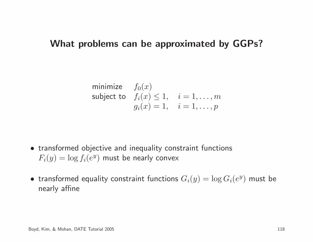
What problems can be approximated by GGPs?
minimize f0(x)subject to fi(x) ≤ 1, i = 1, . . . ,m
gi(x) = 1, i = 1, . . . , p
• transformed objective and inequality constraint functionsFi(y) = log fi(e
y) must be nearly convex
• transformed equality constraint functions Gi(y) = log Gi(ey) must be
nearly affine
Boyd, Kim, & Mohan, DATE Tutorial 2005 118

Monomial fitting via log-regression
find coefficient c > 0 and exponents a1, . . . , an of monomial f so that
f(x(i)) ≈ f (i), i = 1, . . . , N
• rewrite as
log f(x(i)) = log c + a1 log x(i)1 + · · · + an log x(i)
n
≈ log f (i), i = 1, . . . , N
• use least-squares (regression) to find log c, a1, . . . , an that minimize
N∑
i=1
(log c + a1 log x
(i)1 + · · · + an log x(i)
n − log f (i))2
Boyd, Kim, & Mohan, DATE Tutorial 2005 119
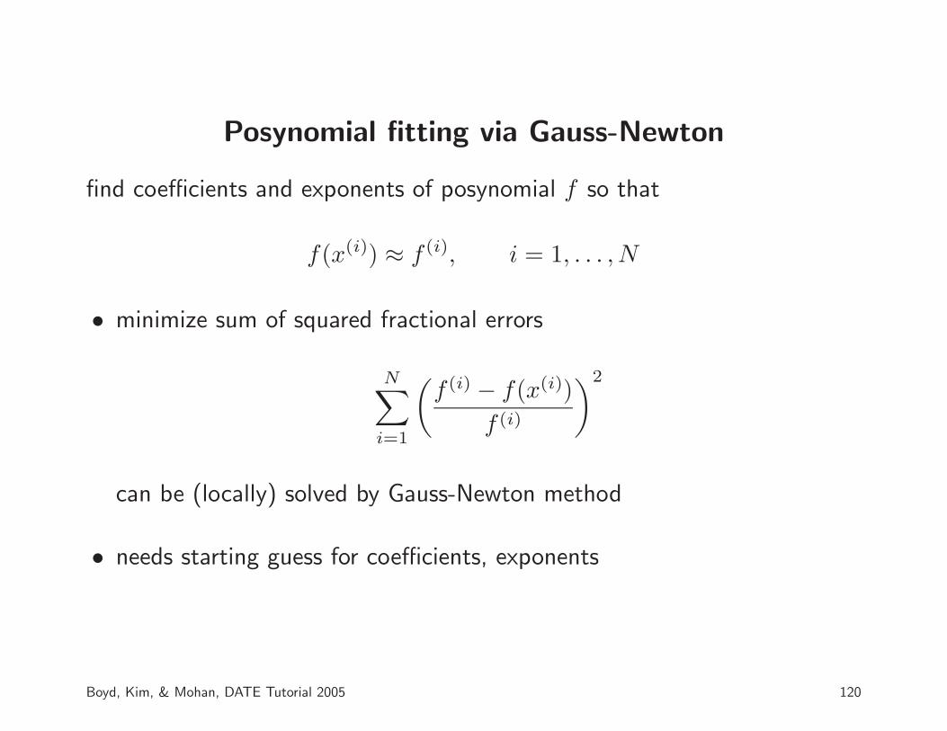
Posynomial fitting via Gauss-Newton
find coefficients and exponents of posynomial f so that
f(x(i)) ≈ f (i), i = 1, . . . , N
• minimize sum of squared fractional errors
N∑
i=1
(f (i) − f(x(i))
f (i)
)2
can be (locally) solved by Gauss-Newton method
• needs starting guess for coefficients, exponents
Boyd, Kim, & Mohan, DATE Tutorial 2005 120
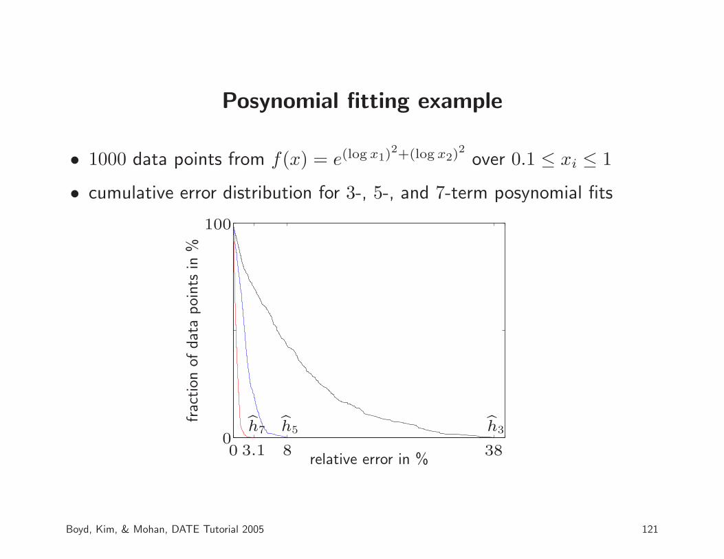
Posynomial fitting example
• 1000 data points from f(x) = e(log x1)2+(log x2)
2over 0.1 ≤ xi ≤ 1
• cumulative error distribution for 3-, 5-, and 7-term posynomial fits
relative error in %
frac
tion
ofdat
apoi
nts
in%
bh3bh5
bh7
0 3.1 8 380
100
Boyd, Kim, & Mohan, DATE Tutorial 2005 121

A simple max-monomial fitting method
fit max-monomialf(x) = max
k=1,...,Kfk(x)
(f1, . . . , fk monomials) to data x(i), f (i), i = 1, . . . , N
simple algorithm:
repeat
for k = 1, . . . , K
1. find all data points x(j) for which fk(x(j)) = f(x(j))
(i.e., data points at which fk is the largest of the monomials)
2. update fk by carrying out monomial fit to these data
Boyd, Kim, & Mohan, DATE Tutorial 2005 122

Max-monomial fitting example
• same 1000 data points as previous example
• cumulative error distribution for 3-, 5-, and 7-term max-monomial fits
relative error in %
frac
tion
ofdat
apoi
nts
in%
0 0.1 0.2 0.3 0.4 0.50
100
bh3bh5
bh7
Boyd, Kim, & Mohan, DATE Tutorial 2005 123

Conclusions

Conclusions
(generalized) geometric programming
• comes up in a variety of circuit sizing contexts
• can be used to formulate a variety of problems
• admits fast, reliable solution of large-scale problems
• is good at concurrently balancing lots of coupled constraints andobjectives
• is useful even when problem has discrete constraints
Boyd, Kim, & Mohan, DATE Tutorial 2005 124
Approach
• most problems don’t come naturally in GP form; be prepared toreformulate and/or approximate
• GP modeling is not a “try my software” method; it requires thinking
• our approach:
– start with simple analytical models (RC, square-law, Pelgrom, . . . )to verify GP might apply
– then fit GP-compatible models to simulation or measured data– for highest accuracy, revert to local method for final polishing
Boyd, Kim, & Mohan, DATE Tutorial 2005 125

• looking for keys under street light(not where keys were lost, but lighting is good)
• forcing problems into GP-compatible form(problems aren’t GPs, but solving is good)
Boyd, Kim, & Mohan, DATE Tutorial 2005 126
References
• A tutorial on geometric programming
• Digital circuit sizing via geometric programming
• Analog circuit design via geometric programming
• Convex optimization, Cambridge Univ. Press 2004
(these include hundreds of references)
available at www.stanford.edu/~boyd/research.html
Boyd, Kim, & Mohan, DATE Tutorial 2005 127

Software
• MOSEK: www.mosek.com
• COPL-GP: (Yinyu Ye, in process of being re-worked):www.stanford.edu/~yyye/Col.html
• GPGLP: ftp://ftp.pitt.edu/dept/ie/GP/
• YALMIP: control.ee.ethz.ch/~joloef/yalmip.msql
• a simple matlab GP solver gp.m at Boyd’s EE364 site
Boyd, Kim, & Mohan, DATE Tutorial 2005 128