getting started with stm32h74xi/g and stm32h75xi/g
TRANSCRIPT

January 2020 AN4938 Rev 5 1/47
1
AN4938Application note
Getting started with STM32H74xI/G and STM32H75xI/G hardware development
Introduction
This application note is intended for system designers who develop applications based on STM32H750 Value line, STM32H742, STM32H743/753, STM32H745/755 and STM32H747/757 lines, and who need an implementation overview of the following hardware features:
• Power supply
• Package selection
• Clock management
• Reset control
• Boot mode settings
• Debug management.
This document describes the minimum hardware resources required to develop an application based on STM32H74xI/G and STM32H75xI/G microcontrollers.
Reference documents
The following documents are available on www.st.com:
• STM32H742xI/G and STM32H743xI/G datasheet
• STM32H745xI/G datasheet
• STM32H747xI/G datasheet
• STM32H750xB datasheet
• STM32H753xI/G datasheet
• STM32H755xI/G datasheet
• STM32H757xI/G datasheet
• Oscillator design guide for STM8S, STM8A and STM32 microcontrollers application note (AN2867)
• STM32 microcontroller system memory boot mode application note (AN2606).
Table 1. Applicable products
Generic part numbers Corresponding product lines
STM32H74xI/G, STM32H75xI/G
STM32H742, STM32H750 Value, STM32H743/753, STM32H745/755, STM32H747/757
www.st.com
Contents AN4938
2/47 AN4938 Rev 5
Contents
1 General information . . . . . . . . . . . . . . . . . . . . . . . . . . . . . . . . . . . . . . . . . 7
2 Power supplies . . . . . . . . . . . . . . . . . . . . . . . . . . . . . . . . . . . . . . . . . . . . . 7
2.1 Introduction . . . . . . . . . . . . . . . . . . . . . . . . . . . . . . . . . . . . . . . . . . . . . . . . 7
2.1.1 Independent analog supply and reference voltage . . . . . . . . . . . . . . . . . 7
2.1.2 USB transceiver independent power supply . . . . . . . . . . . . . . . . . . . . . . 8
2.1.3 Battery backup domain . . . . . . . . . . . . . . . . . . . . . . . . . . . . . . . . . . . . . 10
2.1.4 LDO voltage regulator . . . . . . . . . . . . . . . . . . . . . . . . . . . . . . . . . . . . . . 10
2.1.5 SMPS step-down converter . . . . . . . . . . . . . . . . . . . . . . . . . . . . . . . . . . 11
2.2 Power supply scheme . . . . . . . . . . . . . . . . . . . . . . . . . . . . . . . . . . . . . . . 12
2.3 Reset and power supply supervisor . . . . . . . . . . . . . . . . . . . . . . . . . . . . . 15
2.3.1 Power-on reset (POR)/power-down reset (PDR) . . . . . . . . . . . . . . . . . . 15
2.3.2 Programmable voltage detector (PVD) . . . . . . . . . . . . . . . . . . . . . . . . . 15
2.3.3 Analog voltage detector (AVD) . . . . . . . . . . . . . . . . . . . . . . . . . . . . . . . . 16
2.3.4 System reset . . . . . . . . . . . . . . . . . . . . . . . . . . . . . . . . . . . . . . . . . . . . . 16
2.3.5 Internal power supervisor ON . . . . . . . . . . . . . . . . . . . . . . . . . . . . . . . . 17
2.3.6 Internal power supervisor OFF . . . . . . . . . . . . . . . . . . . . . . . . . . . . . . . 17
2.3.7 Bypass mode . . . . . . . . . . . . . . . . . . . . . . . . . . . . . . . . . . . . . . . . . . . . . 19
3 Alternate function mapping to pins . . . . . . . . . . . . . . . . . . . . . . . . . . . . 20
4 Clocks . . . . . . . . . . . . . . . . . . . . . . . . . . . . . . . . . . . . . . . . . . . . . . . . . . . . 21
4.1 HSE oscillator clock . . . . . . . . . . . . . . . . . . . . . . . . . . . . . . . . . . . . . . . . . 21
4.1.1 External user clock (HSE bypass) . . . . . . . . . . . . . . . . . . . . . . . . . . . . . 22
4.1.2 External crystal/ceramic resonator (HSE crystal) . . . . . . . . . . . . . . . . . 22
4.2 LSE oscillator clock . . . . . . . . . . . . . . . . . . . . . . . . . . . . . . . . . . . . . . . . . 22
4.2.1 External clock (LSE bypass) . . . . . . . . . . . . . . . . . . . . . . . . . . . . . . . . . 23
4.2.2 External crystal/ceramic resonator (LSE crystal) . . . . . . . . . . . . . . . . . . 23
4.3 Clock security system (CSS) . . . . . . . . . . . . . . . . . . . . . . . . . . . . . . . . . . 24
5 Boot configuration . . . . . . . . . . . . . . . . . . . . . . . . . . . . . . . . . . . . . . . . . 25
5.1 Boot mode selection . . . . . . . . . . . . . . . . . . . . . . . . . . . . . . . . . . . . . . . . . 25
5.2 Boot pin connection . . . . . . . . . . . . . . . . . . . . . . . . . . . . . . . . . . . . . . . . . 26
5.3 System bootloader mode . . . . . . . . . . . . . . . . . . . . . . . . . . . . . . . . . . . . . 26

AN4938 Rev 5 3/47
AN4938 Contents
4
6 Debug management . . . . . . . . . . . . . . . . . . . . . . . . . . . . . . . . . . . . . . . . 28
6.1 Introduction . . . . . . . . . . . . . . . . . . . . . . . . . . . . . . . . . . . . . . . . . . . . . . . 28
6.2 SWJ debug port (serial wire and JTAG) . . . . . . . . . . . . . . . . . . . . . . . . . . 28
6.2.1 TPIU trace port . . . . . . . . . . . . . . . . . . . . . . . . . . . . . . . . . . . . . . . . . . . 28
6.2.2 External debug trigger . . . . . . . . . . . . . . . . . . . . . . . . . . . . . . . . . . . . . . 29
6.3 Pinout and debug port pins . . . . . . . . . . . . . . . . . . . . . . . . . . . . . . . . . . . 29
6.3.1 SWJ debug port pins . . . . . . . . . . . . . . . . . . . . . . . . . . . . . . . . . . . . . . . 29
6.3.2 Flexible SWJ-DP pin assignment . . . . . . . . . . . . . . . . . . . . . . . . . . . . . 30
6.3.3 Internal pull-up and pull-down on JTAG pins . . . . . . . . . . . . . . . . . . . . . 31
6.3.4 SWJ debug port connection with standard JTAG connector . . . . . . . . . 31
7 Recommendations . . . . . . . . . . . . . . . . . . . . . . . . . . . . . . . . . . . . . . . . . 32
7.1 Printed circuit board . . . . . . . . . . . . . . . . . . . . . . . . . . . . . . . . . . . . . . . . . 32
7.2 Component position . . . . . . . . . . . . . . . . . . . . . . . . . . . . . . . . . . . . . . . . . 32
7.3 Ground and power supply (VSS,VDD) . . . . . . . . . . . . . . . . . . . . . . . . . . . 32
7.4 Decoupling . . . . . . . . . . . . . . . . . . . . . . . . . . . . . . . . . . . . . . . . . . . . . . . . 32
7.5 Other signals . . . . . . . . . . . . . . . . . . . . . . . . . . . . . . . . . . . . . . . . . . . . . . 33
7.6 Unused I/Os and features . . . . . . . . . . . . . . . . . . . . . . . . . . . . . . . . . . . . 33
8 Reference design . . . . . . . . . . . . . . . . . . . . . . . . . . . . . . . . . . . . . . . . . . 34
8.1 Reference design description . . . . . . . . . . . . . . . . . . . . . . . . . . . . . . . . . . 34
8.1.1 Clocks . . . . . . . . . . . . . . . . . . . . . . . . . . . . . . . . . . . . . . . . . . . . . . . . . . 34
8.1.2 Reset . . . . . . . . . . . . . . . . . . . . . . . . . . . . . . . . . . . . . . . . . . . . . . . . . . . 34
8.1.3 Boot mode . . . . . . . . . . . . . . . . . . . . . . . . . . . . . . . . . . . . . . . . . . . . . . . 34
8.1.4 SWJ interface . . . . . . . . . . . . . . . . . . . . . . . . . . . . . . . . . . . . . . . . . . . . 34
8.1.5 Power supply . . . . . . . . . . . . . . . . . . . . . . . . . . . . . . . . . . . . . . . . . . . . . 34
8.2 Component references . . . . . . . . . . . . . . . . . . . . . . . . . . . . . . . . . . . . . . . 35
9 Recommended PCB routing guidelines for STM32H74xI/G and STM32H75xI/G devices . . . . . . . . . . . . . . . . . . . . . 37
9.1 PCB stack-up . . . . . . . . . . . . . . . . . . . . . . . . . . . . . . . . . . . . . . . . . . . . . . 37
9.2 Crystal oscillator . . . . . . . . . . . . . . . . . . . . . . . . . . . . . . . . . . . . . . . . . . . . 38
9.3 Power supply decoupling . . . . . . . . . . . . . . . . . . . . . . . . . . . . . . . . . . . . . 38
9.4 High speed signal layout . . . . . . . . . . . . . . . . . . . . . . . . . . . . . . . . . . . . . 40
9.4.1 SDMMC bus interface . . . . . . . . . . . . . . . . . . . . . . . . . . . . . . . . . . . . . . 40
9.4.2 Flexible memory controller (FMC) interface . . . . . . . . . . . . . . . . . . . . . . 40

Contents AN4938
4/47 AN4938 Rev 5
9.4.3 Quadrature serial parallel interface (QUADSPI) . . . . . . . . . . . . . . . . . . 41
9.4.4 Embedded trace macrocell (ETM) . . . . . . . . . . . . . . . . . . . . . . . . . . . . . 43
10 Conclusion . . . . . . . . . . . . . . . . . . . . . . . . . . . . . . . . . . . . . . . . . . . . . . . . 44
11 Revision history . . . . . . . . . . . . . . . . . . . . . . . . . . . . . . . . . . . . . . . . . . . 45

AN4938 Rev 5 5/47
AN4938 List of tables
5
List of tables
Table 1. Applicable products . . . . . . . . . . . . . . . . . . . . . . . . . . . . . . . . . . . . . . . . . . . . . . . . . . . . . . . 1Table 2. Boot modes. . . . . . . . . . . . . . . . . . . . . . . . . . . . . . . . . . . . . . . . . . . . . . . . . . . . . . . . . . . . . 25Table 3. STM32H74xI/G and STM32H75xI/G bootloader communication peripherals . . . . . . . . . . 26Table 4. TPIU trace pins . . . . . . . . . . . . . . . . . . . . . . . . . . . . . . . . . . . . . . . . . . . . . . . . . . . . . . . . . . 29Table 5. External debug trigger pins. . . . . . . . . . . . . . . . . . . . . . . . . . . . . . . . . . . . . . . . . . . . . . . . . 29Table 6. SWJ debug port pins . . . . . . . . . . . . . . . . . . . . . . . . . . . . . . . . . . . . . . . . . . . . . . . . . . . . . 30Table 7. Flexible SWJ-DP assignment . . . . . . . . . . . . . . . . . . . . . . . . . . . . . . . . . . . . . . . . . . . . . . . 30Table 8. Mandatory components . . . . . . . . . . . . . . . . . . . . . . . . . . . . . . . . . . . . . . . . . . . . . . . . . . . 35Table 9. Optional components . . . . . . . . . . . . . . . . . . . . . . . . . . . . . . . . . . . . . . . . . . . . . . . . . . . . . 35Table 10. Document revision history . . . . . . . . . . . . . . . . . . . . . . . . . . . . . . . . . . . . . . . . . . . . . . . . . 45

List of figures AN4938
6/47 AN4938 Rev 5
List of figures
Figure 1. VDD33USB connected to VDD power supply . . . . . . . . . . . . . . . . . . . . . . . . . . . . . . . . . . . 9Figure 2. VDD33USB/VDD50USB connected to external power supply . . . . . . . . . . . . . . . . . . . . . . . 9Figure 3. Power supply overview . . . . . . . . . . . . . . . . . . . . . . . . . . . . . . . . . . . . . . . . . . . . . . . . . . . 14Figure 4. Power on reset/power down reset waveform . . . . . . . . . . . . . . . . . . . . . . . . . . . . . . . . . . . 15Figure 5. PVD threshold. . . . . . . . . . . . . . . . . . . . . . . . . . . . . . . . . . . . . . . . . . . . . . . . . . . . . . . . . . . 16Figure 6. Reset circuit . . . . . . . . . . . . . . . . . . . . . . . . . . . . . . . . . . . . . . . . . . . . . . . . . . . . . . . . . . . . 17Figure 7. Power supply supervisor interconnection with
internal power supervisor OFF . . . . . . . . . . . . . . . . . . . . . . . . . . . . . . . . . . . . . . . . . . . . . . 18Figure 8. NRST circuitry timing example . . . . . . . . . . . . . . . . . . . . . . . . . . . . . . . . . . . . . . . . . . . . . . 19Figure 9. STM32CubeMX example screen-shot . . . . . . . . . . . . . . . . . . . . . . . . . . . . . . . . . . . . . . . . 20Figure 10. HSE external clock . . . . . . . . . . . . . . . . . . . . . . . . . . . . . . . . . . . . . . . . . . . . . . . . . . . . . . . 21Figure 11. HSE crystal/ceramic resonators . . . . . . . . . . . . . . . . . . . . . . . . . . . . . . . . . . . . . . . . . . . . . 21Figure 12. LSE external clock . . . . . . . . . . . . . . . . . . . . . . . . . . . . . . . . . . . . . . . . . . . . . . . . . . . . . . . 23Figure 13. LSE crystal/ceramic resonators . . . . . . . . . . . . . . . . . . . . . . . . . . . . . . . . . . . . . . . . . . . . . 23Figure 14. Boot mode selection implementation example . . . . . . . . . . . . . . . . . . . . . . . . . . . . . . . . . . 26Figure 15. Host to board connection . . . . . . . . . . . . . . . . . . . . . . . . . . . . . . . . . . . . . . . . . . . . . . . . . . 28Figure 16. JTAG connector implementation . . . . . . . . . . . . . . . . . . . . . . . . . . . . . . . . . . . . . . . . . . . . 31Figure 17. Typical layout for VDD/VSS pair . . . . . . . . . . . . . . . . . . . . . . . . . . . . . . . . . . . . . . . . . . . . . 33Figure 18. STM32H753XI reference schematic . . . . . . . . . . . . . . . . . . . . . . . . . . . . . . . . . . . . . . . . . 36Figure 19. Four layer PCB stack-up example . . . . . . . . . . . . . . . . . . . . . . . . . . . . . . . . . . . . . . . . . . . 37Figure 20. Six layer PCB stack-up example . . . . . . . . . . . . . . . . . . . . . . . . . . . . . . . . . . . . . . . . . . . . 38Figure 21. Decoupling capacitor placement depending on package type . . . . . . . . . . . . . . . . . . . . . . 39Figure 22. Example of decoupling capacitor placed underneath
the STM32H74xI/G and STM32H75xI/G . . . . . . . . . . . . . . . . . . . . . . . . . . . . . . . . . . . . . . 39

AN4938 Rev 5 7/47
AN4938 General information
46
1 General information
This document applies to STM32H74xI/G and STM32H75xI/G Arm®(a)-based devices.
2 Power supplies
2.1 Introduction
STM32H74xI/G and STM32H75xI/G devices require a 1.71 to 3.6 V operating voltage supply (VDD), which can be reduced down to 1.62 V by using an external power supervisor and connecting PDR_ON pin to VSS (refer to the datasheets for details).
The digital power can be supplied either by a internal system supply voltage regulator or directly by an external supply voltage. This digital power voltage can be set dynamically at different values, the highest value allowing to achieve the maximum performance.
The real-time clock (RTC), the RTC backup registers, and the backup SRAM (BKP SRAM) can be powered from the VBAT voltage (1.2 to 3.6 V) when the main VDD supply is powered OFF.
Note: Refer to the product datasheets for more details on the supply voltage range.
2.1.1 Independent analog supply and reference voltage
To improve analog peripheral performance, the analog peripherals feature an independent power supply which can be separately filtered and shielded from noise on the PCB:
• The analog supply voltage input is available on a separate VDDA pin.
• An isolated supply ground connection is provided on the pin VSSA.
To ensure a better accuracy of low-voltage inputs, the user can connect a separate external reference voltage on VREF+.
In addition, the STM32H74xI/G and STM32H75xI/G microcontrollers embed an internal voltage reference buffer, which can be used as voltage reference for ADCs, DACs, as well as external components through the VREF+ pin. This buffer supports four voltages that can be configured through the VREFBUF_CSR register.
When available (depending on the package), VREF– pin must be externally tied to VSSA.
VDDA minimum value (VDDA_MIN) depends on the analog peripheral and on whether a reference voltage is provided or not:
• If no analog peripheral is used, VDDAmin equals 0 V.
• When an ADC or a comparator is used, VDDA_MIN equals 1.62 V.
• When a DAC is used, VDDA_MIN equals 1.8V.
a. Arm is a registered trademark of Arm Limited (or its subsidiaries) in the US and/or elsewhere.
Power supplies AN4938
8/47 AN4938 Rev 5
• When an OPAMP is used, VDDA_MIN equals 2.0 V.
• When a reference voltage (VREFBUF_OUT) is provided by the device on VREF+ pin, VDDA_MIN depends on the required level for this voltage.
Note: Refer to the product datasheets for more details on VREF+ reference voltage range.
2.1.2 USB transceiver independent power supply
There are different ways to supply the USB transceivers, depending on VDD33USB and VDD50USB availability:
• When the VDD50USB pin is available, this pin can be used to supply an internal regulator dedicated to USB transceivers. In this case, VDD50USB pin should receive a voltage ranging from 4.0 to 5.5 V, typically supplied from the VBUS line of the USB connector. The regulated power (3.0 to 3.6 V) is available on VDD33USB.
In this configuration VDD50USB voltage must respect the following condition:
An external capacitor must be connected to VDD33USB.
• When the VDD33USB pin is available, this pin can be used to supply the internal transceiver. In this case, VDD33USB pin should receive a voltage ranging from 3.0 to 3.6 V. If VDD50USB is also available, it must be connected to VDD33USB. As an example, when the device is powered at 1.8 V, an independent 3.3 V power supply can be applied to VDD33USB.
When VDD33USB is connected to a separate power supply, it is independent from VDD and VDDA. It must be the last supply applied and the first supply switched OFF. The following conditions must be respected (see Figure 2):
– During the power-on and power-down phases (VDD < VDD minimum value), VDD33USB should always be lower than VDD.
– VDD33USB rising and falling time specifications must be respected (refer to table power-up/power-down operating conditions (regulator ON) and table power-up/power-down operating conditions (regulator OFF) provided in the device datasheets).
– In operating mode, VDD33USB can be either lower or higher than VDD:
If a USB interface is used (USB OTG_HS/OTG_FS), the associated GPIOs powered by VDD33USB operate between VDD33USB_MIN and VDD33USB_MAX(see Figure 2).
VDD33USB supplies both USB OTG_HS and USB OTG_FS transceivers. If only one USB transceiver is used in the application, the GPIOs associated to the other USB transceiver are still supplied by VDD33USB.
If no USB interface is used (USB OTG_HS/OTG_FS), the associated GPIOs powered by VDD33USB operate in VDD range (between VDD_MIN and VDD_MAX).
In the above two configurations, an external capacitor must be connected to VDD33USB.
• When neither VDD33USB nor VDD50USB is available, VDD pins are use to supply USB transceivers and must be in the range of 3.0 to 3.6 V for the transceiver to operate correctly.
VDD50USB VDD 300 mV+<

AN4938 Rev 5 9/47
AN4938 Power supplies
46
Figure 1. VDD33USB connected to VDD power supply
Figure 2. VDD33USB/VDD50USB connected to external power supply
1. VDDx can be any power supply voltage among VDDA, VDD33USB, VDD50USB and VDDDSI.
2. If the SMPS is available, VDD and VDDSMPS must be wired together to follow the same voltage sequence.

Power supplies AN4938
10/47 AN4938 Rev 5
2.1.3 Battery backup domain
Backup domain description
To retain the content of the RTC backup registers, backup SRAM, and supply the RTC when VDD is turned off, VBAT pin can be connected to an optional 1.2-3.6 V standby voltage supplied by a battery. Otherwise, VBAT must be connected to another source, such as VDD.
When the backup domain is supplied by VBAT (analog switch connected to VBAT since VDD is not present), the following functions are available:
• PC14 and PC15 can be used as LSE pins only.
• PC13 can be used as tamper pin (TAMP1).
• PI8 can be used as tamper pin (TAMP2).
• PC1 can be used as tamper pin (TAMP3).
During tRSTTEMPO (temporization at VDD startup) or after a power-down reset (PDR) is detected, the power switch between VBAT and VDD remains connected to VBAT.
During the startup phase, if VDD is established in less than tRSTTEMPO and it is higher than VBAT + 0.6 V, a current may be injected into VBAT pin through an internal diode connected between VDD and the power switch (VBAT). If the power supply/battery connected to the VBAT pin cannot support this current injection, it is strongly recommended to connect an external low-drop diode between this power supply and the VBAT pin.
Refer to the device datasheets for the actual value of tRSTTEMPO.
Battery charging
When VDD is present, the external battery connected to VBAT can be charged through an internal resistance. This operation can be performed either through an internal 5 kΩ or 1.5 kΩ resistor. The resistor value can be configured by software.
Battery charging is automatically disabled in VBAT mode.
2.1.4 LDO voltage regulator
The LDO voltage regulator is always enabled after reset with a default output level set to power scale 3 (VOS3). The LDO can operate in three different modes depending on the application operating modes:
• In Run mode, the regulator supplies full power to the core and the digital domain.
• In Stop mode, the regulator supplies low power to the core and to the digital domain, thus preserving the contents of the registers and SRAM.
• In Standby mode, the regulator is powered down. The contents of the registers and SRAM are lost except for those related to the standby circuitry and the backup domain.
In Run and Stop mode, the LDO voltage regulator can be dynamical scaled by software to different voltage levels: VOS0, VOS1, VOS2, and VOS3, SVOS3, SVOS4 or SVOS5.
The LDO regulator requires a capacitor on VCAP pins.

AN4938 Rev 5 11/47
AN4938 Power supplies
46
2.1.5 SMPS step-down converter
To optimize power consumption, some devices embed a high power-efficient DC/DC non-linear switched-mode power supply voltage down-converter regulator. It can be enabled via the SDEN bit of the PWR_CR3 register.
The SMPS can be used to deliver power either in internal or external supply mode.
1. Internal supply mode (Direct mode):
VCORE domain direct supply follows the device system operating modes (Run, Stop and Standby) where the output voltage is set according to the voltage scaling configured via VOS and SVOS bits.
The SMPS can also supply the internal voltage regulator (LDO) in Normal operating mode or High-performance mode according to SDEXTHP bit setting in PWR_CR3.
2. External supply mode
In this mode, the SMPS can be used to supply external circuits. It operates in MR mode (SDEXTHP bit set to 1 in PWR_CR3) in order to achieve a high performance with an output voltage of 2.5 V or 1.8 V (configured through SDLEVEL bits of PWR_CR3).

Power supplies AN4938
12/47 AN4938 Rev 5
2.2 Power supply scheme
Power supplies
• VDD = 1.62 to 3.6 V: external power supply for I/Os, Flash memory and system analog blocks such as reset and PLL
This power supply is provided externally through VDD pins. VDD pins must be connected to VDD with external decoupling capacitors: one single tantalum or ceramic capacitor (of 4.7 µF minimum capacitance) for the package and a 100 nF ceramic capacitor for each VDD pin.
When VDD is lower than 1.71 V, an external reset controller is required.
Note: VDD minimum value of 1.62 V is obtained when the internal reset controller is OFF (refer to Section 2.3.6: Internal power supervisor OFF).
• VSSA, VDDA = 1.62 to 3.6 V: external analog power supplies for ADCs, DACs and OPAMPs.
VDDA pin must be connected to two external decoupling capacitors (100 nF ceramic capacitors and a 1 µF tantalum or ceramic capacitor).
• VDD33USB and VDD50USB: external power supplies for USB transceiver
When VDD50USB is used to provide power, this pin must be connected to the USB connector VBUS line and to a 4.7 µF decoupling capacitor (CIN). In addition, VDD33USB must be connected to a 1 µF capacitor and its maximum ESR should be 600 mΩ.
When VDD33USB is used to power the USB transceiver (3.0 to 3.6 V), if the VDD50USB pin is available, it must connected to VDD33USB, which must be connected to two external decoupling capacitors (a 100 nF ceramic capacitor and a 1 µF tantalum or ceramic capacitor).
• VBAT = 1.2 to 3.6 V: power supply for the RTC, the external 32 kHz oscillator and backup registers (through power switch) when VDD is not present.
The VBAT pin can be connected to the external battery (1.2 V < VBAT < 3.6 V). If no external battery is used, it is mandatory to connect this pin to an external power supply: as an example, VBAT pin can be connected to VDD through a 100 nF external ceramic decoupling capacitor.
• VREF+ external reference voltage for analog peripherals
VREF+ pin can be connected to VDDA external power supply. If a separate external reference voltage is applied to VREF+, a 100 nF and a 1 μF capacitors must be connected on this pin. In all cases, VREF+ must be kept below VDDA. VREF+ lower limit is 2 V when VDDA is above 2 V and the ADC is used, otherwise it is 1.62 V.
• VDDLDO = 1.62 to 3.6 V: external power supply for voltage regulator
When the LDO voltage regulator is enabled, both VCAP1 and VCAP2 pins must be connected to a 2.2 µF ceramic capacitor with a low ESR (< 100 mΩ). It is recommended to connect VCAP1 pin to VCAP2 pin (for more details, refer to Figure 18: STM32H753XI reference schematic).
If VCAP3 is available, it must be connected to the other VCAP pins but not additional capacitor is required. In addition, the VDDLDOx pins must be connected together and to a 4.7 µF tantalum or ceramic capacitor.

AN4938 Rev 5 13/47
AN4938 Power supplies
46
Four additional power supplies and pins are used on devices that feature the SMPS:
• VDDSMPS = 1.62 to 3.6 V: SMPS step-down converter power supply
VDDSMPS must be kept at the same voltage level as VDD.
VDDSMPS pin must be connected to an external 4.7 μF capacitor with a 100 mΩ equivalent series resistance (ESR).
VSSSMPS is the SMPS step-down converter ground.
• VLXSMPS: SMPS step-down converter supply
VLXSMPS output is coupled to a 2.2 μH inductor with a 220 pF external capacitor.
• VFBSMPS = VCORE = 1.8 or 2.5 V: external SMPS step-down converter sense feedback voltage
VFBSMPS input pin must be connected to a 10 μF capacitor with a 20 mΩ ESR.
Note: Refer to the corresponding datasheet for more details regarding the external components required for the SMPS.
Four additional power supplies and pins are available to supply the internal DSI regulator on STM32H7x7I/G devices:
• VDDDSI = 1.8 to 3.6 V: supply voltage for the DSI internal regulator
VDDDSI is the DSI regulator supply input, while VSSDSI is the DSI regulator ground.
• VDD12DSI = 1.15 to 1.3 V: optional supply voltage for the DSI PHY (DSI regulator OFF)
• VCAPDSI: DSI regulator output
To achieve a better dynamic performance of the regulator, VCAPDSI pin must be connected to an external capacitor, which recommended value is 2.2 µF.
Additional precautions can be taken to filter analog noise:
• VDDA can be connected to VDD through a ferrite bead.
• The VREF+ pin can be connected to VDDA through a resistor (typically 47 Ω).

Power supplies AN4938
14/47 AN4938 Rev 5
Figure 3. Power supply overview
1. N corresponds to the number of VDD pins available on the package.
2. The internal DSI regulator and PHY are available only on STM32H7x7I/G microcontrollers.
3. The SMPS is available only on STM32H7x5I/G and STM32H7x7I/G microcontrollers.

AN4938 Rev 5 15/47
AN4938 Power supplies
46
2.3 Reset and power supply supervisor
2.3.1 Power-on reset (POR)/power-down reset (PDR)
The devices have an integrated POR/PDR circuitry that allows a proper operation starting from 1.71 V.
The devices remain in reset mode when VDD is below a specified threshold, VPOR/PDR, without the need for an external reset circuit. For more details concerning the power on/power-down reset threshold, refer to the electrical characteristics of the datasheet.
Figure 4. Power on reset/power down reset waveform
1. tRSTTEMPO is approximately 2.6 ms. VPOR/PDR rising edge is 1.66 V (typical) and VPOR/PDR falling edge is 1.62 V (typical). Refer to the device datasheets for the actual values.
On the packages embedding the PDR_ON pin, the power supply supervisor is enabled by holding PDR_ON high. On the other packages, the power supply supervisor is always enabled.
2.3.2 Programmable voltage detector (PVD)
The PVD can be used to monitor the VDD power supply by comparing it to a threshold selected by the PLS[2:0] bits in the PWR power control register (PWR_CR1).
The PVD is enabled by setting the PVDE bit.
A PVDO flag is available, in the PWR power control/status register (PWR_CSR1), to indicate if VDD is higher or lower than the PVD threshold. This event is internally connected to the EXTI line16 and can generate an interrupt if enabled through the EXTI registers.
The PVD output interrupt can be generated when VDD drops below the PVD threshold and/or when VDD rises above the PVD threshold depending on EXTI line16 rising/falling edge configuration. As an example the service routine could perform emergency shutdown tasks.

Power supplies AN4938
16/47 AN4938 Rev 5
Figure 5. PVD threshold
2.3.3 Analog voltage detector (AVD)
The AVD can be used to monitor VDDA power supply by comparing it to a threshold selected through the ALS[1:0] bits of the PWR power control register (PWR_CR1). The threshold value can be configured to 1.7, 2.1, 2.5 or 2.8 V (refer to the devices datasheets for the actual values).
The AVD is enabled by setting the AVDEN bit in PWR_CR1 register. An interrupt can be raised when VDDA goes above or below the configured threshold.
2.3.4 System reset
A system reset sets all the registers to their default values except the reset flags in the clock controller RCC_RSR register and the registers in the backup domain (see Figure 6).
A system reset (nreset signal) resets all registers to their default values except for the reset flags in the clock controller RCC_RSR (or RCC_C1_RSR) register and the registers in the backup domain.
A system reset can be generated when one of the following events occurs:
• A low level on the NRST pin (external reset)
• A reset from the brownout reset block via the pwr_bor_rst internal signal
• The input voltage (VDD) drops below a threshold level (pwr_por_rst)
• The independent watchdog end-of-count condition (iwdg1_out_rst)
• A window watchdog end -of-count condition (wwdg1_out_rst)
• A reset from low-power mode (lpwr_rst)
• A software reset from the Arm® Cortex®-M7 core, generated via the SFTRESET signal.

AN4938 Rev 5 17/47
AN4938 Power supplies
46
Figure 6. Reset circuit
2.3.5 Internal power supervisor ON
On the packages embedding the PDR_ON pin, the power supply supervisor is enabled by holding PDR_ON high. On the other packages, the power supply supervisor is always enabled.
For more details about the internal power supervisor ON, refer to the datasheets.
2.3.6 Internal power supervisor OFF
This feature is available only on the packages featuring the PDR_ON pin. The internal power-on reset (POR) / power-down reset (PDR) circuitry is disabled through the PDR_ON pin.
An external power supply supervisor should monitor VDD and NRST and should maintain the device in reset mode as long as VDD is below a specified threshold. PDR_ON should be connected to VSS. Refer to Figure 7: Power supply supervisor interconnection with internal power supervisor OFF.

Power supplies AN4938
18/47 AN4938 Rev 5
Figure 7. Power supply supervisor interconnection with internal power supervisor OFF
The supply ranges which never go below 1.71 V minimum should be better managed by the internal circuitry (no additional component needed, thanks to the fully embedded reset controller).
When the internal reset is OFF, the following integrated features are no more supported:
• The integrated power-on reset (POR) / power-down reset (PDR) circuitry is disabled.
• The brownout reset (BOR) circuitry must be disabled.
• The embedded programmable voltage detector (PVD) is disabled.
• VBAT functionality is no more available and VBAT pin should be connected to VDD.
All the packages, except for the LQFP100, allow to disable the internal reset through the PDR_ON signal when connected to VSS.

AN4938 Rev 5 19/47
AN4938 Power supplies
46
Figure 8. NRST circuitry timing example
2.3.7 Bypass mode
The power management unit can be bypassed. This feature can be configured by software. When bypassed, the core power supply should be provided through VCAPx pins connected together.
In Bypass mode, the internal voltage scaling is not managed internally, and the external voltage value must be consistent with the targeted maximum frequency (see datasheet for the actual VOS level).
In Standby mode the external source will be switched off and the VCORE domains powered down. The external source will be switched on when exiting Standby mode.
In Bypass mode, the external voltage must be present before or at the same time as VDDLDO. To avoid conflict with the LDO, the external voltage must be kept above 1.15 V until the LDO is disabled by software.
Alternate function mapping to pins AN4938
20/47 AN4938 Rev 5
3 Alternate function mapping to pins
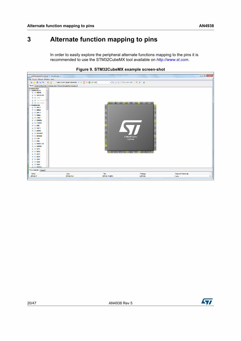
In order to easily explore the peripheral alternate functions mapping to the pins it is recommended to use the STM32CubeMX tool available on http://www.st.com.
Figure 9. STM32CubeMX example screen-shot

AN4938 Rev 5 21/47
AN4938 Clocks
46
4 Clocks
Four different clock sources can be used to drive the system clock (SYSCLK):
• HSI oscillator clock
• CSI oscillator clock.
• HSE oscillator clock
• Main PLL (PLL) clock
The devices have the two following secondary clock sources:
• 32 kHz low-speed internal RC (LSI RC) which drives the independent watchdog and, optionally, the RTC used for Auto-wakeup from the Stop/Standby mode.
• 32.768 kHz low-speed external crystal (LSE crystal) which optionally drives the RTC clock (RTCCLK).
Each clock source can be switched ON or OFF independently when it is not used, to optimize power consumption.
Refer to device reference manual for a detailed description of the clock tree. In particular, a complete view of clock usage by peripheral is provided in the Kernel clock distribution overview.
4.1 HSE oscillator clock
The high speed external clock signal (HSE) can be generated from two possible clock sources:
• HSE external user clock (see Figure 10).
• HSE external crystal/ceramic resonator (see Figure 11).
The resonator and the load capacitors have to be placed as close as possible to the oscillator pins in order to minimize the output distortion and startup stabilization time. The loading capacitance values must be adjusted according to the selected resonator.
Figure 10. HSE external clock Figure 11. HSE crystal/ceramic resonators
Clocks AN4938
22/47 AN4938 Rev 5
4.1.1 External user clock (HSE bypass)
In this mode, an external clock source must be provided. The user selects this mode by setting the HSEBYP and HSEON bits in the RCC clock control register (RCC_CR). The external clock signal (square, sinus or triangle) with ~50% duty cycle has to drive the OSC_IN pin.
4.1.2 External crystal/ceramic resonator (HSE crystal)
The external oscillator frequency ranges from 4 to 48 MHz. The external oscillator has the advantage of producing a very accurate main clock. The associated hardware configuration is shown in Figure 11. Using a 25 MHz oscillator frequency is a good choice to get accurate Ethernet, USB OTG high-speed peripheral, I2S and SAI.
The resonator and the load capacitors have to be connected as close as possible to the oscillator pins in order to minimize the output distortion and startup stabilization time. The load capacitance values must be adjusted according to the selected oscillator.
For CL1 and CL2 it is recommended to use high-quality ceramic capacitors in the 5 pF to 25 pF range (typical), designed for high-frequency applications and selected to meet the requirements of the crystal or resonator. CL1 and CL2, are usually the same value. The crystal manufacturer typically specifies a load capacitance that is the series combination of CL1 and CL2. The PCB and MCU pin capacitances must be included when sizing CL1 and CL2 (10 pF can be used as a rough estimate of the combined pin and board capacitance).
The HSERDY flag in the RCC clock control register (RCC_CR) indicates if the high-speed external oscillator is stable or not. At startup, the clock is not released until this bit is set by hardware. An interrupt can be generated if enabled in the RCC clock interrupt register (RCC_CIR).
If it is not used as clock source, the HSE crystal can be switched ON and OFF using the HSEON bit in the RCC clock control register (RCC_CR).
4.2 LSE oscillator clock
The low-speed external clock signal (LSE) can be generated from two possible clock sources:
• LSE user external clock (see Figure 12).
• LSE external crystal/ceramic resonator (see Figure 13).

AN4938 Rev 5 23/47
AN4938 Clocks
46
1. Figure 13: LSE crystal/ceramic resonators: To avoid exceeding the maximum value of CL1 and CL2 (15 pF) it is strongly recommended to use a resonator with a load capacitance CL ≤ 7 pF.
2. Figure 12: LSE external clock and Figure 13: LSE crystal/ceramic resonators: OSC32_IN and OSC32_OUT pins can be used also as GPIO, but it is recommended not to use them as both RTC and GPIO pins in the same application.
The LSE oscillator is switched ON and OFF using the LSEON bit in RCC backup domain control register (RCC_BDCR).
The LSE includes new modes that can be configured through the LSEDRV [1:0] in RCC_BDCR register to obtain the best trade-off between power consumption and start-up time:
• 00: Low drive.
• 10: Medium low drive.
• 01: Medium high drive.
• 11: High drive.
The LSERDY flag in the RCC backup domain control register (RCC_BDCR) indicates if the LSE crystal is stable or not. At startup, the LSE crystal output clock signal is not released until this bit is set by hardware. An interrupt can be generated if enabled in the RCC clock interrupt register (RCC_CIR).
4.2.1 External clock (LSE bypass)
The LSE bypass mode is available in all system power modes. An external clock source must be provided in LSE bypass mode. It must have a frequency up to 1 MHz. The user selects this mode by setting the LSEBYP and LSEON bits in the RCC backup domain control register (RCC_BDCR). The external clock signal (square, sinus or triangle) with ~50% duty cycle has to drive the OSC32_IN pin (see Figure 12.).
4.2.2 External crystal/ceramic resonator (LSE crystal)
The LSE crystal is a 32.768 kHz low-speed external crystal or ceramic resonator. It has the advantage of providing a low-power, but highly accurate clock source to the real-time clock peripheral (RTC) for clock/calendar or other timing functions.
The resonator and the load capacitors have to be connected as close as possible to the oscillator pins in order to minimize the output distortion and startup stabilization time. The load capacitance values must be adjusted according to the selected oscillator.
Figure 12. LSE external clock Figure 13. LSE crystal/ceramic resonators

Clocks AN4938
24/47 AN4938 Rev 5
4.3 Clock security system (CSS)
The device provides two clock security systems (CSS), one for HSE oscillator and one for LSE oscillator. They can be independently enabled by software.
When the clock security system on HSE is enabled, the clock detector is activated after the HSE oscillator startup delay, and disabled when this oscillator is stopped:
• If the HSE oscillator is used directly or indirectly as the system clock (indirectly meaning that it is directly used as PLL input clock, and that PLL clock is the system clock) and a failure is detected, then the system clock switches to the HSI oscillator and the HSE oscillator is disabled.
• If a failure is detected on the HSE clock, this oscillator is automatically disabled, a clock failure event is sent to the break inputs of advanced-control timers TIM1, TIM8, TIM15, TIM16, and TIM17, and a non-maskable interrupt is generated to inform the software about the failure (clock security system interrupt rcc_hsecss_it), allowing the MCU to perform rescue operations. The rcc_hsecss_it is linked to the Cortex®-M7 NMI (non-maskable interrupt) exception vector.
• If the HSE oscillator clock was used as PLL clock source, the PLL is also disabled when the HSE fails.
The clock security system on LSE must be enabled only when the LSE is enabled and ready, and after the RTC clock has been selected through the RTCSRC[1:0] bits of RCC_BDCR register.
When an LSE failure is detected, the CSS on LSE wakes up the device from all low-power modes except VBAT. If the failure occurred in VBAT mode, the software can check the failure detection bit when the device is powered on again. In all cases the software can select the best behavior (including disabling the CSS on LSE which is not automatic).

AN4938 Rev 5 25/47
AN4938 Boot configuration
46
5 Boot configuration
5.1 Boot mode selection
In STM32H74xI/G and STM32H75xI/G microcontrollers, two different boot spaces can be selected through the BOOT pin and the boot base address programmed in the BOOT_ADD0 or BOOT_ADD1 option bytes as shown in the Table 2.
The BOOT_ADD0 and BOOT_ADD1 address option bytes allow to program any boot memory address from 0x0000 0000 to 0x3FFF 0000 which include:
• All the Flash memory address space mapped on AXIM interface.
• All the RAM address space: ITCM, DTCM RAMs and SRAMs mapped on AXIM interface.
• The system memory bootloader.
The BOOT_ADD0/BOOT_ADD1 option bytes can be modified after the reset in order to boot from any other boot address after the next reset.
If the programmed boot memory address is out of the memory mapped area or a reserved area, the default boot fetch address is programmed as follows:
• Boot address 0: Flash memory at 0x0800 0000
• Boot address 1: ITCM-RAM at 0x0000 0000
When the Flash level 2 protection is enabled, only boot from Flash memory is available. If the boot address already programmed in the BOOT_ADD0 / BOOT_ADD1 option bytes is out of the memory range or belongs to the RAM address range, the default fetch will be forced from Flash memory at address 0x0800 0000.
Note: When the Secure access mode is enabled through option bytes, the boot behavior differs from the above description (refer to section Root secure services of the product reference manual).
Table 2. Boot modes
Boot mode selection
Boot spaceBOOT
pinBoot address option bytes
0 BOOT_ADD0 [15:0]Boot address defined by BOOT_ADD0[15:0] user option byte
Default factory programmed value: User Flash memory starting at 0x0800 0000
1 BOOT_ADD1 [15:0]Boot address defined by BOOT_ADD1[15:0] user option byte
Default factory programmed value: System Flash memory starting at 0x1FF0 0000

Boot configuration AN4938
26/47 AN4938 Rev 5
5.2 Boot pin connection
Figure 14 shows the external connection required to select the boot memory of STM32H74xI/G and STM32H75xI/G microcontrollers.
Figure 14. Boot mode selection implementation example
1. Resistor values are given only as a typical example.
5.3 System bootloader mode
The embedded bootloader code is located in the system memory. It is programmed by ST during production. It is used to reprogram the Flash memory using one of the following serial interfaces.
Table 3 shows the supported communication peripherals by the system bootloader.
Table 3. STM32H74xI/G and STM32H75xI/G bootloader communication peripherals
Bootloader peripherals Bootloader pins
DFU USB OTG FS (PA11/PA12) in device mode
USART1 PA9/PA10
USART2 PA2/PA3
USART3 PB10/PB11
CAN2 PH13/PH14
I2C1 PB6/PB9
I2C2 PF0/PF1
I2C3 PA8/PC9
I2C4 PD12/PD13
SPI1 PA4/PA5/PA6/PA7
SPI2 PI0/PI1/PI2/PI3

AN4938 Rev 5 27/47
AN4938 Boot configuration
46
SPI3 PC12/PC11/PC10/PA15
SPI4 PE11 / PE12 / PE13 / PE14
USB OTG_FS in Device mode (DFU)
PA11/PA12
Table 3. STM32H74xI/G and STM32H75xI/G bootloader communication peripherals
Bootloader peripherals Bootloader pins

Debug management AN4938
28/47 AN4938 Rev 5
6 Debug management
6.1 Introduction
The host/target interface is the hardware equipment that connects the host to the application board. This interface is made of three components: a hardware debug tool, a JTAG or SW connector and a cable connecting the host to the debug tool. Figure 15 shows the connection of the host to the evaluation board.
Figure 15. Host to board connection
6.2 SWJ debug port (serial wire and JTAG)
The core of STM32H74xI/G and STM32H75xI/G devices integrates the Serial Wire / JTAG Debug Port (SWJ-DP). It is an ARM® standard CoreSight debug port that combines a 5-pin JTAG-DP interface and a 2-pin SW-DP interface.
• The JTAG Debug Port (JTAG-DP) provides a 5-pin standard JTAG interface to the AHP-AP port.
• The Serial Wire Debug Port (SW-DP) provides a 2-pin (clock + data) interface to the AHP-AP port.
In the SWJ-DP, the two JTAG pins of the SW-DP are multiplexed with some of the five JTAG pins of the JTAG-DP.
For more details on the SWJ debug port refer to RM0433 SWJ debug port section (serial wire and JTAG).
6.2.1 TPIU trace port
The TPIU trace port comprises four data outputs plus one clock output. The number of data outputs can be configured by software and unused signals can be reused as GPIOs. If the trace port is not required, all the signals can be used as GPIOs. By default, the trace port is disabled.
The trace data and clock can operate at up to 133 MHz. As a result, care must be taken with the layout of these signals: the trace connector should be located as close as possible to the

AN4938 Rev 5 29/47
AN4938 Debug management
46
STM32H74xI/G and STM32H75xI/G, while still allowing enough space to attach the trace port analyzer probe.
Refer to Table 4 for a summary of trace pins and GPIO assignment.
6.2.2 External debug trigger
The TRGIN and TRGOUT pins are available on some packages. On smaller packages, they are replaced by a bidirectional TRGIO signal, which is configured as TRGIN or TRGOUT by software.
Refer to Table 5 for a summary of trigger pins and GPIO assignment.
6.3 Pinout and debug port pins
STM32H74xI/G and STM32H75xI/G devices are available in various packages with different numbers of available pins. As a result, some functionality related to the pin availability (TPIU parallel output interface) may differ between the packages.
6.3.1 SWJ debug port pins
Five pins are used as outputs from the STM32H74xI/G and STM32H75xI/G devices for the SWJ-DP as alternate functions of general-purpose I/Os. These pins are available on all packages.
Table 4. TPIU trace pins
Trace pin name Type Description Pin assignment
TRACED0 Output Trace synchronous data out 0 PC1 or PE3 or PG13
TRACED1 Output Trace synchronous data out 1 PC8 or PE4 or PG14
TRACED2 Output Trace synchronous data out 2 PD2 or PE5
TRACED3 Output Trace synchronous data out 3 PC12 or PE6
TRACECLK Output Trace clock PE2
Table 5. External debug trigger pins
Trigger pin name Type Description Pin assignment
TRGIN Input External trigger input PJ7
TRGOUT Output External trigger output PJ12
TRGIO Input/output External trigger bi-directional PC7

Debug management AN4938
30/47 AN4938 Rev 5
6.3.2 Flexible SWJ-DP pin assignment
After RESET (SYSRESETn or PORESETn), all the five pins used for the SWJ-DP are assigned as dedicated pins immediately usable by the debugger host (note that the trace outputs are not assigned except if explicitly programmed by the debugger host).
However, the STM32H74xI/G and STM32H75xI/G devices offer the possibility of disabling some or all of the SWJ-DP ports and so, of releasing the associated pins for general-purpose IO (GPIO) usage.
Table 7 shows the different possibilities to release some pins.
For more details on how to disable SWJ-DP port pins, please refer to the reference manual I/O pin alternate function multiplexer and mapping section.
Table 6. SWJ debug port pins
SWJ-DP pin nameJTAG debug port SW debug port Pin
assignmentType Description Type Debug assignment
JTMS/SWDIO IJTAG test mode
SelectionIO
Serial wire data
input/outputPA13
JTCK/SWCLK I JTAG test clock I Serial wire clock PA14
JTDI I JTAG test data input - - PA15
JTDO/TRACESWO OJTAG test data
output-
TRACESWO if asynchronous trace is
enabledPB3
NJTRST I JTAG test nReset - - PB4
Table 7. Flexible SWJ-DP assignment
Available debug ports
SWJ IO pin assigned
PA13/JTMS/SWDIO
PA14/JTCK/SWCLK
PA15/JTDI PB3/JTDO PB4/NJTRST
Full SWJ (JTAG-DP + SW-DP) - reset state X X X X X
Full SWJ (JTAG-DP + SW-DP) but without NJTRST
X X X X-
JTAG-DP disabled and SW-DP enabled X X -
JTAG-DP disabled and SW-DP disabled Released

AN4938 Rev 5 31/47
AN4938 Debug management
46
6.3.3 Internal pull-up and pull-down on JTAG pins
The devices embed internal pull-ups and pull-downs to guarantee a correct JTAG behavior. The following pins are consequently not left floating during reset and they are configured as follows until the user software takes control of them:
• NJTRST: internal pull-up.
• JTDI: internal pull-up.
• JTMS/SWDIO: internal pull-up.
• TCK/SWCLK: internal pull-down.
If these I/Os are externally connected to a different voltage, leakage current will flow during and after reset, until they are reconfigured by software. Special care must be taken with the TCK/SWCLK pin, which is directly connected to the clock of some of these flip-flops, since it should not toggle before JTAG I/O is released by the user software.”
6.3.4 SWJ debug port connection with standard JTAG connector
Figure 16 shows the connection between STM32H74xI/G and STM32H75xI/G devices and a standard JTAG connector.
Figure 16. JTAG connector implementation

Recommendations AN4938
32/47 AN4938 Rev 5
7 Recommendations
7.1 Printed circuit board
For technical reasons, it is best to use a multilayer printed circuit board (PCB) with a separate layer dedicated to the ground (VSS) and another dedicated to the VDD supply. This provides a good decoupling and a good shielding effect. For many applications, economical reasons prohibit the use of this type of board. In this case, the major requirement is to ensure a good structure for the ground and for the power supply.
7.2 Component position
A preliminary layout of the PCB must separate the different circuits according to their EMI contribution in order to reduce the cross-coupling on the PCB, that is noisy, high-current circuits, low-voltage circuits, and digital components.
7.3 Ground and power supply (VSS,VDD)
Every block (noisy, low-level sensitive, digital, etc.) should be grounded individually and all ground returns should be to a single point. Loops must be avoided or have a minimum area. The power supply should be implemented close to the ground line to minimize the area of the supply loop. This is due to the fact that the supply loop acts as an antenna, and is therefore the main transmitter and receiver of EMI. All component-free PCB areas must be filled with additional grounding to create a kind of shielding (especially when using single-layer PCBs).
7.4 Decoupling
All the power supply and ground pins must be properly connected to the power supplies. These connections, including pads, tracks and vias should have as low impedance as possible. This is typically achieved with thick track widths and, preferably, the use of dedicated power supply planes in multilayer PCBs.
In addition, each power supply pair should be decoupled with filtering ceramic capacitors (100 nF) and one single tantalum or ceramic capacitor (min. 4.7 μF) connected in parallel. These capacitors need to be placed as close as possible to, or below, the appropriate pins on the underside of the PCB. Typical values are 10 nF to 100 nF, but the exact values depend on the application needs. Figure 17 shows the typical layout of such a VDD/VSS pair.

AN4938 Rev 5 33/47
AN4938 Recommendations
46
Figure 17. Typical layout for VDD/VSS pair
7.5 Other signals
When designing an application, the EMC performance can be improved by closely studying:
• Signals for which a temporary disturbance affects the running process permanently (the case of interrupts and handshaking strobe signals, and not the case for LED commands). For these signals, a surrounding ground trace, shorter lengths and the absence of noisy and sensitive traces nearby (crosstalk effect) improve the EMC performance. For digital signals, the best possible electrical margin must be reached for the two logical states and slow Schmitt triggers are recommended to eliminate parasitic states.
• Noisy signals (clock, etc.).
• Sensitive signals (high impedance, etc.).
7.6 Unused I/Os and features
All the microcontrollers are designed for a variety of applications and often a particular application does not use 100% of the MCU resources. To increase the EMC performance, unused clocks, counters or I/Os, should not be left free, e.g. I/Os should be set to “0” or “1” (pull-up or pull-down to the unused I/O pins.) and unused features should be “frozen” or disabled.

Reference design AN4938
34/47 AN4938 Rev 5
8 Reference design
8.1 Reference design description
The reference design shown in Figure 18 is based on the STM32H753XI, a highly integrated microcontroller that combines the ARM® Cortex®-M7 32-bit RISC core running at up to 400 MHz with up to 2 Mbyte dual-bank Flash memory and 1 Mbytes of RAM (including 192 Kbytes of TCM RAM, 864 Kbytes of user RAM and 4 Kbytes of backup SRAM).
This reference design can be easy ported to other devices. Specific requirements must be respected for the following devices:
• Devices featuring the SMPS: four additional pins must be used to supply the internal SMPS block (refer to the corresponding datasheet for more details).
• Devices featuring a DSI internal regulator: four additional pins must be used to supply the internal DSI regulator block (refer to the corresponding datasheet for more details).
8.1.1 Clocks
Two clock sources are used for the microcontroller:
• LSE: X1– 32.768 kHz crystal for the embedded RTC.
• HSE: X2– 25 MHz crystal.
Refer to Section 4: Clocks on page 21.
8.1.2 Reset
The reset signal of STM32H753XI device is low active and the reset sources include:
• Reset button B1
• Debugging Tools from JTAG/SWD connector CN15 and ETM trace connector CN12
Refer to Section 2.3: Reset and power supply supervisor on page 15.
8.1.3 Boot mode
Refer to Section 5: Boot configuration on page 25.
8.1.4 SWJ interface
Refer to Section 6: Debug management on page 28.
8.1.5 Power supply
Refer to Section 2: Power supplies on page 7.

AN4938 Rev 5 35/47
AN4938 Reference design
46
8.2 Component references
Table 8. Mandatory components
Id Component name Reference Quantity Comments
1 Microcontroller STM32H753XI 1 TFBGA240 package
2 Capacitor 100 nF 20Ceramic capacitors (decoupling capacitors)
3 Capacitor 4.7 µF 1Ceramic capacitor (decoupling capacitor)
4 Capacitor 2.2 µF 2Ceramic capacitor (regulator capacitor)
Table 9. Optional components
Id Components
nameReference Quantity Comments
1 Resistor 10 kΩ 5 Pull-up and pull-down for JTAG, BOOT pin, PDR
2 Resistor 0 Ω 1Used as star connection point between VDDA and VREF+
3 Capacitor 100 nF 4 Ceramic capacitor
4 Capacitor 1.5 pF 2Used for LSE: the value depends on the crystal characteristics
5 Capacitor 1 μF 3 Used for VDDA, VREF and VDDUSB
6 Capacitor 3.9 pF 2Used for HSE: the value depends on the crystal characteristics
7 Quartz 25 MHz 1 Used for HSE
8 Quartz 32.768 kHz 1 Used for LSE
9 JTAG connector
HE10-20 1 –
10 Battery 3 V 1If no external battery is used in the application, it is recommended to connect VBAT externally to VDD.
11 Switch SPDT 1 Used to select the right boot mode.
12 Push-button B1 1 Reset button
13 Jumper 3 pins 2 Used to select VBAT source
14 Ferrite beadFCM1608KF
-601T031 Additional decoupling for VDDA

Refere
nc
e d
esig
nA
N4938
36/4
7A
N49
38 Rev 5
Figure 18. STM32H753XI reference schematic

AN4938 Rev 5 37/47
AN4938 Recommended PCB routing guidelines for STM32H74xI/G and STM32H75xI/G devices
46
9 Recommended PCB routing guidelines for STM32H74xI/G and STM32H75xI/G devices
9.1 PCB stack-up
In order to reduce the reflections on high speed signals, it is necessary to match the impedance between the source, sink and transmission lines. The impedance of a signal trace depends on its geometry and its position with respect to any reference planes.
The trace width and spacing between differential pairs for a specific impedance requirement is dependent on the chosen PCB stack-up. As there are limitations in the minimum trace width and spacing which depend on the type of PCB technology and cost requirements, a PCB stack-up needs to be chosen which allows all the required impedances to be realized.
The minimum configuration that can be used is 4 or 6 layers stack-up. An 8 layers boards may be required for a very dense PCBs that have multiple SDRAM/SRAM/NOR/LCD components.
The following stack-ups are intended as examples which can be used as a starting point for helping in a stack-up evaluation and selection. These stack-up configurations are using a GND plane adjacent to the power plane to increase the capacitance and reduce the gap between GND and power plane. So high speed signals on top layer will have a solid GND reference plane which helps to reduce the EMC emissions, as going up in number of layers and having a GND reference for each PCB signal layer will improve further the radiated EMC performance.
Figure 19. Four layer PCB stack-up example

Recommended PCB routing guidelines for STM32H74xI/G and STM32H75xI/G devices AN4938
38/47 AN4938 Rev 5
Figure 20. Six layer PCB stack-up example
9.2 Crystal oscillator
Use the application note: Oscillator design guide for STM8S, STM8A and STM32 microcontrollers (AN2867), for further guidance on how to layout and route crystal oscillator circuits.
9.3 Power supply decoupling
An adequate power decoupling for STM32H74xI/G and STM32H75xI/G devices is necessary to prevent an excessive power noise and ground bounce noise. Please refer to Section 2.2: Power supply scheme.
The following recommendations shall be followed:
• Place the decoupling capacitors as close as possible to the power and ground pins of the MCU. For BGA packages, it is recommended to place the decoupling capacitors on the other side of the PCB (see Figure 21).
• Add the recommended decoupling capacitors for as many VDD/GND pairs as possible.
• Connect the decoupling capacitor pad to the power and ground plane with a wider, short trace/via. This allows reducing the series inductance, maximizing the current flow and minimizing the transient voltage drops from the power plane which also reduces the possibility of ground bounce.
Figure 22 shows an example of decoupling capacitor placement underneath STM32H74xI/G and STM32H75xI/G devices, closer to the pins and with less vias.

AN4938 Rev 5 39/47
AN4938 Recommended PCB routing guidelines for STM32H74xI/G and STM32H75xI/G devices
46
Figure 21. Decoupling capacitor placement depending on package type
Figure 22. Example of decoupling capacitor placed underneath the STM32H74xI/G and STM32H75xI/G
Recommended PCB routing guidelines for STM32H74xI/G and STM32H75xI/G devices AN4938
40/47 AN4938 Rev 5
9.4 High speed signal layout
9.4.1 SDMMC bus interface
Interface connectivity
The SD/SDIO MMC card host interface (SDMMC) provides an interface between the AHB peripheral bus and Multi Media Cards (MMCs), SD memory cards and SDIO cards. The SDMMC interface is a serial data bus interface, that consists of a clock (CK), command signal (CMD) and 8 data lines (D[0:7]).
Interface signal layout guidelines
• Reference the plane using GND or PWR (if PWR, add 10nf switching cap between PWR and GND)
• Trace the impedance: 50 Ω ± 10%
• The skew being introduced into the clock system by unequal trace lengths and loads, minimize the board skew, keep the trace lengths equal between the data and clock.
• The maximum skew between data and clock should be below 250 ps @ 10mm
• The maximum trace length should be below 120 mm. If the signal trace exceeds this trace-length/speed criterion, then a termination should be used
• The trace capacitance should not exceed 20 pF at 3.3 V and 15 pF at 1.8 V
• The maximum signal trace inductance should be less than 16 nH
• Use the recommended pull-up resistance for CMD and data signals to prevent bus floating.
• The mismatch within data bus, data and CK or CK and CMD should be below 10mm.
• Keep the same number of vias between the data signals
Note: The total capacitance of the SD memory card bus is the sum of the bus master capacitance CHOST, the bus capacitance CBUS itself and the capacitance CCARD of each card connected to this line. The total bus capacitance is CL= CHost + CBus + N*CCard where the host is an STM32H74xI/G and STM32H75xI/G device, bus is all the signals and Card is SD card.
9.4.2 Flexible memory controller (FMC) interface
Interface connectivity
The FMC controller and in particular SDRAM memory controller which has many signals, most of them have a similar functionality and work together. The controller I/O signals could be split in four groups as follow:
• An address group which consists of row/column address and bank address
• A command group which includes the row address strobe (NRAS), the column address strobe (NCAS), and the write enable (SDWE)
• A control group which includes a chip select bank1 and bank2 (SDNE0/1), a clock enable bank1 and bank2 (SDCKE0/1), and an output byte mask for the write access (DQM).
• A data group/lane which contains 8 signals (b): the eight D (D7–D0) and the data mask (DQM).

AN4938 Rev 5 41/47
AN4938 Recommended PCB routing guidelines for STM32H74xI/G and STM32H75xI/G devices
46
Interface signal layout guidelines
• Reference the plane using GND or PWR (if PWR, add 10nf stitching cap between PWR and GND
• Trace the impedance: 50 Ω ± 10%
• The maximum trace length should be below 120mm. If the signal trace exceeds this trace-length/speed criterion, then a termination should be used
• Reduce the crosstalk, place data tracks on the different layers from the address and control lanes, if possible. However, when the data and address/control tracks coexist on the same layer they must be isolated from each other by at least 5 mm.
• Match the trace lengths for the data group within ± 10 mm of each other to diminish the skew. Serpentine traces (back and forth traces in an “S” pattern to increase trace length) can be used to match the lengths.
• Placing the clock (SDCLK) signal on an internal layer, minimizes the noise (EMI). Route the clock signal at least 3x of the trace away from others signals. Use as less vias as possible to avoid impedance change and reflection. Avoid using serpentine routing.
• Match the clock traces to the data/address group traces within ±10mm.
• Match the clock traces to each signal trace in the address and command groups to within ±10mm (with maximum of <= 20 mm).
• Trace the capacitances:
– At 3.3 V keep the trace within 20 pF with overall capacitive loading (including Data, Address, SDCLK and Control) no more than 30 pF.
– At 1.8 V keep the trace within 15 pF with overall capacitive loading (including Data, Address, SDCLK and Control) no more than 20 pF.
9.4.3 Quadrature serial parallel interface (QUADSPI)
Interface connectivity
The QUADSPI is a specialized communication interface targeting single, dual or QUADSPI FLASH memories. The QUADSPI interface is a serial data bus interface, that consists of a clock (SCLK), a chip select signal (nCS) and 4 data lines (IO[0:3]).
b.It depends of the used memory: SDRAM with x8 bus widths have only one data group, while x16 and x32 bus-width SDRAM have two and four lanes, respectively.

Recommended PCB routing guidelines for STM32H74xI/G and STM32H75xI/G devices AN4938
42/47 AN4938 Rev 5
Interface signal layout guidelines
• Reference the plane using GND or PWR (if PWR, add 10nf stitching cap between PWR and GND
• Trace the impedance: 50 Ω ± 10%
• The maximum trace length should be below 120mm. If the signal trace exceeds this trace-length/speed criterion, then a termination should be used
• Avoid using multiple signal layers for the data signal routing.
• Route the clock signal at least 3x of the trace away from other signals. Use as less vias as possible to avoid the impedance change and reflection. Avoid using a serpentine routing.
• Match the trace lengths for the data group within ± 10 mm of each other to diminish skew. Serpentine traces (back and forth traces in an “S” pattern to increase trace length) can be used to match the lengths.

AN4938 Rev 5 43/47
AN4938 Recommended PCB routing guidelines for STM32H74xI/G and STM32H75xI/G devices
46
• Avoid using a serpentine routing for the clock signal and as less via(s) as possible for the whole path. a via alters the impedance and adds a reflection to the signal.
9.4.4 Embedded trace macrocell (ETM)
Interface connectivity
The ETM enables the reconstruction of the program execution. The data are traced using the data watchpoint and trace (DWT) component or the instruction trace macrocell (ITM) whereas instructions are traced using the embedded trace macrocell (ETM). The ETM interface is synchronous with the data bus of 4 lines D[0:3] and the clock signal CLK.
Interface signals layout guidelines
• Reference the plane using GND or PWR (if PWR, add 10nf stitching cap between PWR and GND
• Trace the impedance: 50 Ω ± 10%
• All the data trace should be as short as possible (<=25 mm),
• Trace the lines which should run on the same layer with a solid ground plane underneath it without a via.
• Trace the clock which should have only point-to-point connection. Any stubs should be avoided.
• It is strongly recommended also for other (data) lines to be point-to-point only. If any stubs are needed, they should be as short as possible. If longer are required, there should be a possibility to optionally disconnect them (e.g. by jumpers).
Conclusion AN4938
44/47 AN4938 Rev 5
10 Conclusion
This application note should be used as a reference when starting a new design with an STM32H74xI/G and STM32H75xI/G microcontroller.

AN4938 Rev 5 45/47
AN4938 Revision history
46
11 Revision history
Table 10. Document revision history
Date Revision Changes
13-Jun-2017 1 Initial release.
26-Jan-2018 2Added Section 1: General information.
Updated Figure 18: STM32H753XI reference schematic.
18-Mar-2019 3
Document generalized to all STM32H74xx and STM32H75xx.
Added Table 1: Applicable products on cover page.
Added Arm notice in Section 1: General information.
Updated Section 2.1: Introduction and Section 2.2: Power supply scheme. Updated references to notes in Figure 3: Power supply overview.
Updated Figure 4: Power on reset/power down reset waveform, Section 2.3.4: System reset and Section 2.3.7: Bypass mode.
Updated Section 4.1: HSE oscillator clock.
Updated Section 4.2: LSE oscillator clock.
Updated Figure 16: JTAG connector implementation and Figure 18: STM32H753XI reference schematic.

Revision history AN4938
46/47 AN4938 Rev 5
09-May-2019 4
Added VSO0 in Section 2.1.4: LDO voltage regulator.
Added SMPS:
– Added note 2. below Figure 2: VDD33USB/VDD50USB connected to external power supply.
– Added Section 2.1.5: SMPS step-down converter.
– Added VDDSMPS, VLXSMPS and VFBSMPS in Section 2.2: Power supply scheme.
– Updated Figure 3: Power supply overview.
– Updated Section 8.1: Reference design description.
Added DSI:
– Added VDDDSI in note 1. below Figure 2: VDD33USB/VDD50USB connected to external power supply.
– Added VDDDSI and VDD12DSI in Section 2.2: Power supply scheme.
– Updated Figure 3: Power supply overview.
– Updated Section 8.1: Reference design description.
Changed the number of 100 nF capacitors to 4 in Table 9: Optional components.
Updated Figure 18: STM32H753XI reference schematic and removed Table Reference connection for all packages.
16-Jan-2020 5
Updated Figure 3: Power supply overview to change the capacitor between VDD33USB and GND to 1 µF.
Replaced internal reset ON by internal power supervisor ON in Section 2.3.5: Internal power supervisor ON.
Replaced internal reset OFF by internal power supervisor OFF in Section 2.3.6: Internal power supervisor OFF.
Updated Section 2.3.7: Bypass mode.
Updated Section 4.2.1: External clock (LSE bypass).
Updated Figure 18: STM32H753XI reference schematic to tie F1 to VSS.
Updated LSE and HSE clock crystals in Section 8.1.1: Clocks.
Table 10. Document revision history
Date Revision Changes
AN4938 Rev 5 47/47
AN4938
47
IMPORTANT NOTICE – PLEASE READ CAREFULLY
STMicroelectronics NV and its subsidiaries (“ST”) reserve the right to make changes, corrections, enhancements, modifications, and improvements to ST products and/or to this document at any time without notice. Purchasers should obtain the latest relevant information on ST products before placing orders. ST products are sold pursuant to ST’s terms and conditions of sale in place at the time of order acknowledgement.
Purchasers are solely responsible for the choice, selection, and use of ST products and ST assumes no liability for application assistance or the design of Purchasers’ products.
No license, express or implied, to any intellectual property right is granted by ST herein.
Resale of ST products with provisions different from the information set forth herein shall void any warranty granted by ST for such product.
ST and the ST logo are trademarks of ST. For additional information about ST trademarks, please refer to www.st.com/trademarks. All other product or service names are the property of their respective owners.
Information in this document supersedes and replaces information previously supplied in any prior versions of this document.
© 2020 STMicroelectronics – All rights reserved