global power sicepitaxial wafer mission statement power sic epitaxial wafer group is committed to...
TRANSCRIPT
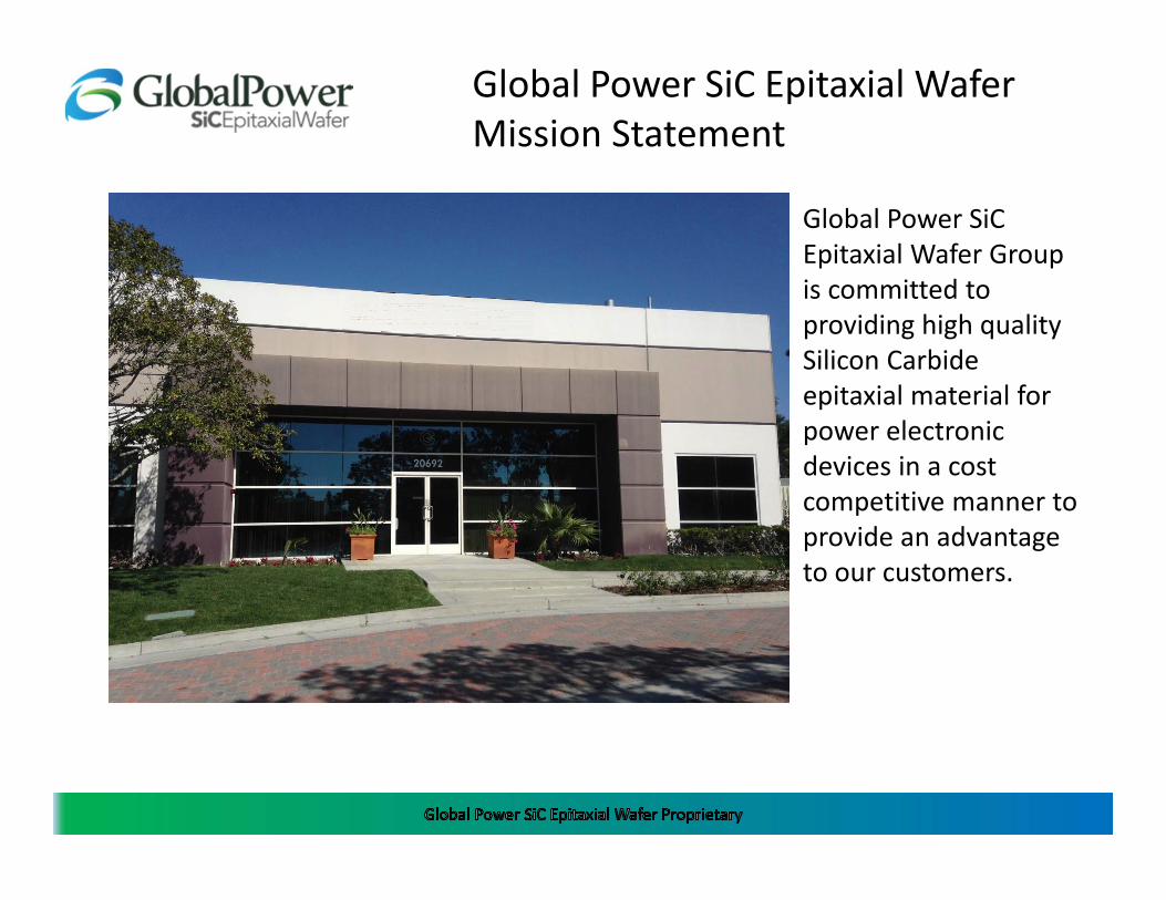
Global Power SiCEpitaxial Wafer Group is committed to providing high quality Silicon Carbide epitaxial material for power electronic devices in a cost competitive manner to provide an advantage to our customers.
Global Power SiC Epitaxial Wafer Mission Statement
Global Power SiC Epitaxial Wafer
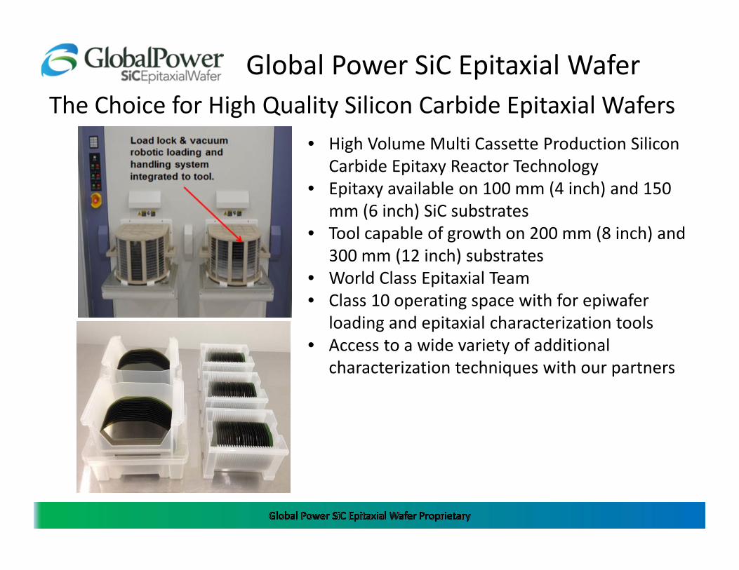
• High Volume Multi Cassette Production Silicon Carbide Epitaxy Reactor Technology
• Epitaxy available on 100 mm (4 inch) and 150 mm (6 inch) SiC substrates
• Tool capable of growth on 200 mm (8 inch) and 300 mm (12 inch) substrates
• World Class Epitaxial Team • Class 10 operating space with for epiwafer
loading and epitaxial characterization tools• Access to a wide variety of additional
characterization techniques with our partners
The Choice for High Quality Silicon Carbide Epitaxial Wafers

Spectral Reflectance for Epi Thickness MeasurementsImaging System For Defect Analysis
Capacitance Voltage for Epi Doping Measurements
• Spectral Reflectance is Faster, Cheaper and More Reliable Than FTIR• High Point Density Wafer Mapping Capability With Rapid
Throughput
• State of the Art CV Tool Uses Hg Based Contacts for Measurement• Wafer Mapping Capability With No Permanent Contacts on Wafer
Surface
Defect Inspection Tool• Can measure 100 mm &150 mm
wafers• High Resolution Imaging
Microscope Collects Thousands of Images for Defect Analysis
• Microscope pictures linked to defect map for easy location of images
• Software mapping easy to set up• Provides full wafer color defect
maps• Measurement speed
• 100 mm wafer 2000+ pictures ~ 20 minutes
• 150 mm wafer 4500+ pictures ~ 45 minutes
• Defect analysis data exportable to csv
Example of a Detected Defect (Triangle)
SiC Epitaxy Characterization Tools

4
Manufacturing Data (100 mm Substrates)

5
• GPTG epiwafer technology verses a leading Competitor’s epiwafers
• Thickness Uniformity is Comparable• Doping Uniformity is Superior!• Defect Control is Comparable*
*Note: Competitor yield is based on counts of what they refer to as “Killer Defects”. GPTG yield is based on all observable defects on the epiwafer surface.
GPTG’s Epiwafers Beat the Competition

6
150 mm Epi Growth Runs
7
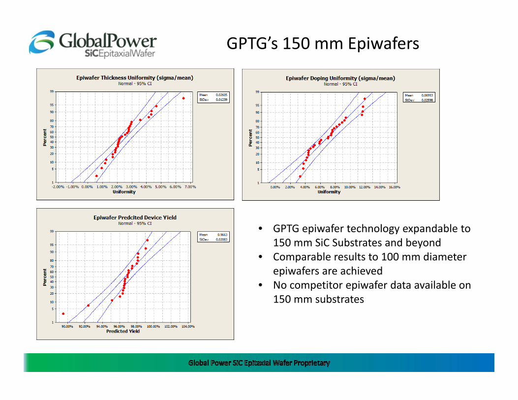
• GPTG epiwafer technology expandable to 150 mm SiC Substrates and beyond
• Comparable results to 100 mm diameter epiwafers are achieved
• No competitor epiwafer data available on 150 mm substrates
GPTG’s 150 mm Epiwafers

8
200 mm SiC Substrates

9
GPTGs epitaxy tool can grow on 200 mm substrates today!
200 mm SiC substrates are under active development at II‐VI

10
Summary
• GPTGs epitaxy reactor is in production on 100 mm SiCsubstrates today.
• Doping uniformity, in particular, is better than commercially available epitaxy.
• Sampling customers on 150 mm substrate epitaxymaterial now and can move to production as soon as the market is ready.
• We can leap ahead of the market using 200 mm SiCsubstrates and above with the right partner.