graphene and hexa boron nitride heterostacks and beyond · 2014-10-20 · graphene and hexa boron...
TRANSCRIPT

Graphene and Hexa Boron Nitride Heterostacks and Beyond
Philip Kim
Physics Department, Columbia University

Beginning of Graphene Research
Geim & Novoselov
Submitted 19 July 2004; accepted 15 September 2004
2010 Physics

Various 2D van der Waals Systems
X
X
M
C
BN
graphene
hexa-BN
Metal-Chalcogenide
M = Ta, Nb, Fe, Co, Mo, …
X = S, Se, Te, …
Bi2Sr2CaCu2O8-x
Charge Transfer Bechgaard Salt
(TMTSF)2PF6
Lead Halide Layered Organic
Semiconducting materials: WSe2, NbS2, MoS2, … Complex-metallic compounds : TaSe2, TaS2, … Magnetic materials: FeSe2, CoSe2 ,…Superconducting: NbSe2, Bi2Sr2CaCu2O8-x, ZrNCl,…


Boron Nitridegraphene
Band Gap Dielectric Constant Optical Phonon Energy Structure
BN 5.5 eV ~4 >150 meV Layered crystal
SiO2 8.9 eV 3.9 59 meV Amorphous
Comparison of h-BN and SiO2
hexa-Boron Nitride: Ideal Dielectric

Co-lamination and Transfer Techniques
1. spin coat substrate with PMMA and scratch onto top surface
2. Lift off PMMA; graphene comes with it!
3. Align graphene over target using a micro-manipulator. PMMA is brought into contact with target and annealed.
Dean et al. Nature Nano (2010)

Flat Graphene on hBN
BNgraphene
0.5 um
Roughness
-0.4 -0.2 0.0 0.2 0.40.0
0.4
0.8
1.2
Graphene BN
frequ
ency
[a.u
.]
height [nm]
0.22 nm
2 um

Room temperature mobility >100,000 cm2V-1s-1
Extremely High Mobility in Graphene/BN

Graphene Integer and Fractional Quantum Hall Effect
5 m
Dean et al. Nature Phys (2011)Young et al., Nature Phys (2012)
0 1 0 2 0 3 0-5 0
0
5 0
1 0 0
1 5 0
3 4 5
(K
)
B (T )
Broken Sym Integer QHE Gaps FQHE Gaps
4/3 ~ 50K
* Spontaneous broken SU(4) symmetrydue to many body correlation
* Energy Scale is big
4 ~ 200 K
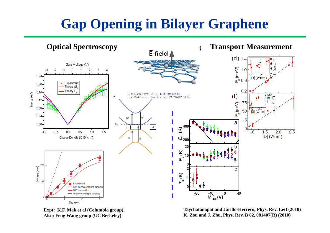
Gap Opening in Bilayer Graphene
Expt: K.F. Mak et al (Columbia group), Also: Feng Wang group (UC Berkeley)
Optical Spectroscopy Transport Measurement
Taychatanapat and Jarillo-Herrero, Phys. Rev. Lett (2010)K. Zou and J. Zhu, Phys. Rev. B 82, 081407(R) (2010)

>200 meV transport gaps may be possible!
-2 0 20.0
5.0x10⁴
1.0x10⁵
1.5x10⁵
2.0x10⁵
2.5x10⁵
3.0x10⁵
BG = -50 V -40 V -30 V -20 V -10 V 0 V 10 V 20 V 30 V 40 V 50 V
Rxx
(Ohm
s)
VTG (Volts)
4-terminalvoltage bias
0 1 2 3
0
20
40
60
80
100
120
2-Terminal ConductanceVBG = -60 Volts
Ixx
(nA)
Vgate (Volts)
BN top and bottom gate
Gap Opening in Bilayer Graphene / hBN
T =1.7 K
Wang et al. (Hone, Kim, Shepard) (2012)

BN/Graphene/BN/Graphene/BN
Kim, Tutuc, PRB (2011); Tse, Das Sarma PRB (2007)
0 5 10 15 20 25-10
-5
0
5
10
RD
rag (
Ohm
s)
VBG (Volts)
224.91 K 201.96 K 175.15 K 148.37 K 98.53 K 75.48 K 48.54 K 25.23 K 11.26 K
I+ VDrag
I-Coulomb Drag Configuration
grnd
0 5 10 15 20 25
63
50
38
25
13
0
row
50 100 150 200 250
-5
0
5
5 V 10 V 11.5 V 18.5 V 20 V 25 V
RD
rag (
Ohm
s)
Temperature (K)
BN tunneling junction/ Drag DeviceDean et al. (Hone, Kim, Shepard) (2011)
Maher et al. (2012)
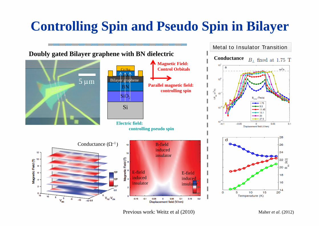
Controlling Spin and Pseudo Spin in Bilayer
5 m
Si
SiO2
BNBilayer graphene
BNCr/Au
Doubly gated Bilayer graphene with BN dielectric
Electric field: controlling pseudo spin
Parallel magnetic field: controlling spin
Conductance
Metal to Insulator Transition
Previous work: Weitz et al (2010)
Conductance ()
Magnetic Field:Control Orbitals
E-field induced insulator
B-field induced insulator
E-field induced insulator
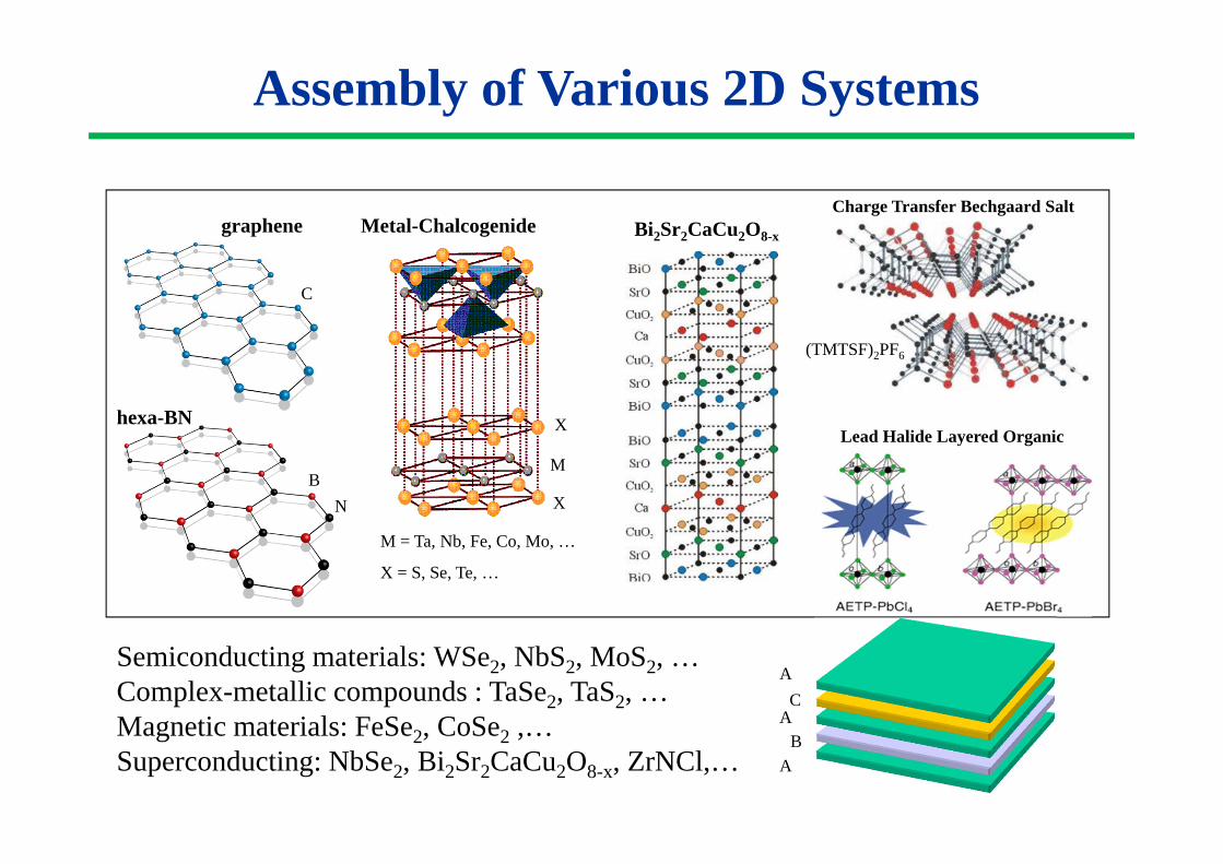
Assembly of Various 2D Systems
X
X
M
C
BN
graphene
hexa-BN
Metal-Chalcogenide
M = Ta, Nb, Fe, Co, Mo, …
X = S, Se, Te, …
Bi2Sr2CaCu2O8-x
Charge Transfer Bechgaard Salt
(TMTSF)2PF6
Lead Halide Layered Organic
Semiconducting materials: WSe2, NbS2, MoS2, … Complex-metallic compounds : TaSe2, TaS2, … Magnetic materials: FeSe2, CoSe2 ,…Superconducting: NbSe2, Bi2Sr2CaCu2O8-x, ZrNCl,… A
BA
CA

Yang et al. Science in press (2012)
Graphene/Silicon hybrid Device: Graphene Barristors
Gate Variable Schottky Diode
Invertor and half adder is demonstrated!

Layered Semiconductor: MoS2
Band Gap ~ 1. 8 eVMobility ~ 200 cm2/Vsec
Radisavljevic et al., Nature Nano (2011)

Choi et al. in preparation (2012)
Controlled Charge Trapping by Ultrathin MoS2 Layers in Graphene/hBN/MoS2 Heterostructured Memory Devices
Floating MoS2 Gate
Hysteresis due to Controlled Charge Trapping
Memory Device Operation

SummaryGraphene on hBN Bilayer gapped device Double layer Coulomb drag
Controlled Charge TrapEmploying MoS2 Layer
Metal/Insulator Transition
Graphene/ NbSe2Tunable Graphene/Si Schottky Diode

Acknowledgement
Funding:
Past MembersMelinda Han (Ph.D. 2010, Frontier of Science Fellow, Columbia University)Meninder S. Purewal (Ph.D. 2008)Josh Small (Ph.D. 2006)Yuanbo Zhang (Ph.D. 2006, Professor, Fundan University)Yuri Zuev (Ph.D. 2011, IBM Fishkill)Kirill Bolotin (Assistant Professor, Department of Physics, Vanderbilt University)Byung Hee Hong (Associate Professor, Department of Chemistry, Seoul National University) Pablo Jarillo-Herrero (Assistant Professor, Department of Physics, MIT)Keunsoo Kim (Assistant Professor, Department of Physics, Sejong University)Namdong Kim (Research Scientist, POSTECH)Barbaros Oezyilmaz (Assistant Professor, Department of Physics, National University of Singapore)
Current MembersYue ZhaoMitsuhide TakekoshiAndrea YoungDmitri EfetovFereshte GhahariPatrick MaherYoung-Jun Yu (jointly with GRL, POSTECH)Vikram Deshpande (jointly with Hone group)Paul Cadden-Zimansky (Columbia Frontier of Science Fellow)Chenguang Lu (jointly with Hone and Herman
Collaborating Students/postodcsCory Dean, Inanc Meric, Lei Wang, Sebastian Sorgenfrei, Kevin Knox, Nayung Jung, Seok Ju Kang, Jun Yan, Yanwen Tan, Kevin Knox
CollaboratorsHorst Stormer, Aron Pinczuk, Tony Heinz, Abhay Pasupathy, Latha VenkataramanLouis Brus, George Flynn, Colin Nuckolls, Jim Hone, Ken Shepard, Louis Campos, Rick OsgoodT. Taniguchi, K, WatanabeAndre Geim, Kostya Novoselov, Sanka Das Sarma
Kim group and friends (2011)