graphene-based nanoelectronics (fy11) - u.s. army ... nanoelectronics (fy11) 5a. contract number 5b....
TRANSCRIPT

Graphene-based Nanoelectronics (FY11)
by Dr. Madan Dubey, Dr. Raju Nambaru, Dr. Marc Ulrich,
Dr. Matthew Ervin, Dr. Barbara Nichols, Mr. Eugene Zakar, Dr. Osama M. Nayfeh, Mr. Matthew Chin, Dr. Glen Birdwell, Dr. Terrance O’Regan, Dr. Tony Ivanov, and Dr. Robert Proie
ARL-TR-5873 January 2012 Approved for public release; distribution unlimited.

NOTICES
Disclaimers The findings in this report are not to be construed as an official Department of the Army position unless so designated by other authorized documents. Citation of manufacturer’s or trade names does not constitute an official endorsement or approval of the use thereof. Destroy this report when it is no longer needed. Do not return it to the originator.
Army Research Laboratory Adelphi, MD 20783-1197
ARL-TR-5873 January 2012
Graphene-based Nanoelectronics (FY11)
Dr. Madan Dubey Sensors and Electron Devices Directorate, ARL
Dr. Raju Nambaru
Computational and Information Sciences Directorate, ARL
Marc Ulrich Army Research Office
Contributors:
Dr. Matthew Ervin, Dr. Barbara Nichols, Mr. Eugene Zakar, Dr. Osama M. Nayfeh, Mr. Matthew Chin, Dr. Glen Birdwell, Dr. Terrance O’Regan, Dr. Tony Ivanov, and Dr. Robert Proie
Sensors and Electron Devices Directorate, ARL Approved for public release; distribution unlimited.

ii
REPORT DOCUMENTATION PAGE Form Approved OMB No. 0704-0188
Public reporting burden for this collection of information is estimated to average 1 hour per response, including the time for reviewing instructions, searching existing data sources, gathering and maintaining the data needed, and completing and reviewing the collection information. Send comments regarding this burden estimate or any other aspect of this collection of information, including suggestions for reducing the burden, to Department of Defense, Washington Headquarters Services, Directorate for Information Operations and Reports (0704-0188), 1215 Jefferson Davis Highway, Suite 1204, Arlington, VA 22202-4302. Respondents should be aware that notwithstanding any other provision of law, no person shall be subject to any penalty for failing to comply with a collection of information if it does not display a currently valid OMB control number. PLEASE DO NOT RETURN YOUR FORM TO THE ABOVE ADDRESS.
1. REPORT DATE (DD-MM-YYYY)
January 2012 2. REPORT TYPE
DSI 3. DATES COVERED (From - To)
October 2010 to September 2011 4. TITLE AND SUBTITLE
Graphene-based Nanoelectronics (FY11) 5a. CONTRACT NUMBER
5b. GRANT NUMBER
5c. PROGRAM ELEMENT NUMBER
6. AUTHOR(S)
Dr. Madan Dubey, Dr. Raju Nambaru, Dr. Marc Ulrich, Dr. Matthew Ervin, Dr. Barbara Nichols, Mr. Eugene Zakar, Dr. Osama M. Nayfeh, Mr. Matthew Chin, Dr. Glen Birdwell, Dr. Terrance O’Regan, Dr. Tony Ivanov, and Dr. Robert Proie
5d. PROJECT NUMBER
5e. TASK NUMBER
5f. WORK UNIT NUMBER
7. PERFORMING ORGANIZATION NAME(S) AND ADDRESS(ES)
U.S. Army Research Laboratory ATTN: RDRL-SER-L 2800 Powder Mill Road Adelphi, MD 20783-1197
8. PERFORMING ORGANIZATION REPORT NUMBER ARL-TR-5873
9. SPONSORING/MONITORING AGENCY NAME(S) AND ADDRESS(ES)
10. SPONSOR/MONITOR’S ACRONYM(S)
11. SPONSOR/MONITOR’S REPORT NUMBER(S)
12. DISTRIBUTION/AVAILABILITY STATEMENT
Approved for public release; distribution unlimited.
13. SUPPLEMENTARY NOTES
14. ABSTRACT
A large program in graphene-based nanoelectronics has continued at the U.S. Army Research Laboratory (ARL) under the auspices of the ARL Director’s Strategic Initiative (DSI). An array of capabilities for graphene growth, characterization, device fabrication, and device modeling has been established, and expertise has been gained in all facets of this research. Significant results have been achieved, including growth of single-, bi-, and few-layer graphene; development of a graphene transfer process; development of atomic layer deposition of dielectrics for graphene devices; and the modeling, designing, and fabricating of graphene-based field effect transistors with radio frequency (RF) performance up to 3 GHz. This research could potentially have enormous benefits for the American Soldier including smaller and more efficient power electronics and communication systems, transparent and flexible electronics, and wearable electronics. 15. SUBJECT TERMS
Graphene, nanoelectronics, single layer, multilayers, grapheme nanoribbons, ALD, ambipolar, Director’s Strategic Initiative (DSI)
16. SECURITY CLASSIFICATION OF: 17. LIMITATION
OF ABSTRACT
UU
18. NUMBER OF PAGES
76
19a. NAME OF RESPONSIBLE PERSON Madan Dubey
a. REPORT
Unclassified b. ABSTRACT
Unclassified c. THIS PAGE
Unclassified 19b. TELEPHONE NUMBER (Include area code) (301) 394-1186
Standard Form 298 (Rev. 8/98) Prescribed by ANSI Std. Z39.18

iii
Contents
List of Figures vi
List of Tables viii
Acknowledgments ix
1. Introduction 1
1.1 Collaboration ...................................................................................................................3
2. Graphene Growth 4
2.1 Chemical Vapor Deposition Furnaces .............................................................................4
2.2 Growth on Copper ...........................................................................................................5
2.2.1 Objectives ............................................................................................................5
2.2.2 Introduction .........................................................................................................5
2.2.3 Experimental Description ....................................................................................6
2.2.4 Results and Analysis ...........................................................................................8
2.2.5 Conclusion/Summary ........................................................................................14
2.2.6 Future Work ......................................................................................................14
2.3 Growth on Nickel ..........................................................................................................15
2.3.1 Introduction .......................................................................................................15
2.3.2 Experimental Procedure ....................................................................................15
2.3.3 Ni Film Preparation ...........................................................................................16
2.3.4 Ni Annealing .....................................................................................................16
2.3.5 Role of H2 in the APCVD Process ....................................................................17
2.3.6 Graphene Growth ..............................................................................................18
2.3.7 Raman Spectroscopy .........................................................................................21
2.3.8 Conclusions .......................................................................................................22
2.3.9 Summary ...........................................................................................................23
2.3.10 Proposed Work FY12 ........................................................................................23
3. Characterization by Raman Spectroscopy 24
3.1 Introduction ...................................................................................................................24
3.2 Theory and Concept ......................................................................................................24
3.2.1 Optical Properties ..............................................................................................24

iv
3.2.2 Phonons .............................................................................................................25
3.2.3 Raman Scattering ..............................................................................................27
3.2.4 Macroscopic Theory of Raman Scattering ........................................................28
3.2.5 Phonon Dispersion Relations of Graphene .......................................................30
3.2.6 Graphene Raman Features .................................................................................32
3.3. Current Status ................................................................................................................34
3.3.1 “Rules-of-Thumb” for Raman Spectral Analysis of Graphene .........................34
3.3.2 Established Raman Mapping Capability ...........................................................36
3.4 Results ...........................................................................................................................37
3.4.1 Raman Mapping and Device Fabrication ..........................................................37
3.5 Next Steps: Planned Goals with Time Line ..................................................................37
3.5.1 Experimental .....................................................................................................37
3.5.2 Modeling ...........................................................................................................38
4. Radio Frequency (RF) CVD Graphene FETs 38
4.1 Experiment and Discussion ...........................................................................................38
4.1.1 Graphene Field Effect Transistors with a 3-GHz Current Cut-off Frequency ..38
4.1.2 Graphene Field Effect Transistors using Boron Nitride Substrates ..................40
4.2 Summary .......................................................................................................................41
4.3 FY-2012 Proposed Work Timeline ...............................................................................41
5. Carbon Nanotube/Graphene Supercapacitors 42
5.1 Introduction ...................................................................................................................42
5.2 Experimental Description ..............................................................................................43
5.3 Result Analysis ..............................................................................................................46
5.4 Conclusion .....................................................................................................................48
5.5 Summary .......................................................................................................................49
5.6 FY12 Proposed Work and Timeline ..............................................................................49
6. Simulation and Modeling 49
7. Conclusions 50
7.1 Transitions .....................................................................................................................50
7.2 Future Research .............................................................................................................50
8. References 52

v
List of Symbols, Abbreviations, and Acronyms 59
Distribution List 63

vi
List of Figures
Figure 1. Graphene is a 2-D building material for graphitic materials of all other dimensionalities. It can be wrapped up into 0-D buckyballs, rolled into 1-D nanotubes, or stacked into 3-D graphite (1). ....................................................................................................1
Figure 2. Raman spectra comparison of graphene after transfer onto a SiO2/Si substrate, after acetone vaporization (ACE Vapor), and after thermal annealing at 500 °C. .............................9
Figure 3. AFM height images of graphene (a) after transfer onto a SiO2/Si substrate, (b) after acetone vaporization (ACE vapor), and (c) after annealing at 300 °C. ...................................10
Figure 4. Raman spectra of transferred graphene on SiO2/Si annealed at 250, 300, 400, and 500 °C. .....................................................................................................................................11
Figure 5. AFM height images of transferred graphene annealed at 300 °C under various gas flows: (a) 1700 sccm H2/1700 sccm Ar, (b) 700 sccm H2/500 sccm Ar, (c) 1700 sccm H2/500 sccm Ar, and (d) 700 sccm H2/1700 sccm Ar. ............................................................12
Figure 6. IG’/IG values for graphene after transfer, after acetone vaporization (ACE Vapor), and after thermal annealing at 300 to 500 °C. ........................................................................13
Figure 7. AFM image of Ni morphology before CVD growth of graphene by method of (a) evaporation, (b) sputtering 2 mT, 100 °C, (c) sputtering 20 mT, 100 °C, and (d) sputtering 2 mT, 250 °C. ....................................................................................................16
Figure 8. Morphology of (a) equilateral grains from evaporation; (b) 30% large grain from sputtering, 2 mT and 100 °C; and (c) 50% large grains from sputtering, 20 mT and 100 °C. .....................................................................................................................................17
Figure 9. Excess H2 leads to pinholes in Ni catalyst. ...................................................................18
Figure 10. Distribution of graphene patches on top of (a) evaporated Ni with equilateral grains; (b) occupancy 30% large grains from sputtered, 2 mT and 100 °C; and (c) occupancy 50% large grains from sputtered, 20 mT and 100 °C deposit conditions. ........19
Figure 11. Size comparison of multilayer graphene patches grown and annealed at (a) 975 °C and (b) 950 °C from an evaporated Ni template. ..................................................20
Figure 12. Comparison of images according to (a) clear or transparent, (b) light, (c) medium, and (d) dark graphene patches on evaporated Ni surface. .......................................................21
Figure 13. Comparison of Raman intensity peaks according to (a) clear or transparent, (b) light, (c) medium, and (d) dark graphene patches on Ni. ...................................................21
Figure 14. Schematic diagram illustrating the linear optical processes that occur at the surface and in the interior of a semiconductor. ........................................................................25
Figure 15. One-dimensional diatomic chain with lattice constant a. ............................................25
Figure 16. The dispersion relation for the 1-D diatomic chain. ....................................................27
Figure 17. Honeycomb lattice of graphene. ...................................................................................31
Figure 18. Calculated phonon dispersion relation of graphene showing the iLO, iTO, oTO, iLA, iTA, and oTA phonon branches (60). ..............................................................................32

vii
Figure 19. Raman spectrum of a graphene edge, showing the main Raman features, the D/D’, G and G’ bands (60). .....................................................................................................33
Figure 20. (Left) First-order G-band process and (center) one-phonon second-order double resonance (DR) process for the D-band (intervalley process) (top) and D’-band (intravalley process) (bottom) and (right) two-phonon second-order resonance Raman spectral processes (top) for the DR G’ process and (bottom) triple resonance (TR) G’ band process for monolayer graphene (76). For one-phonon, second-order transitions, one of the two scattering events is an elastic scattering event. Resonance points are shown as open circles near the K point (left) and the K’ point (right) (60). ...........................................33
Figure 21. (a) Raman spectra of exfoliated graphene for several different layer numbers and bulk (HOPG) graphite. (b) Raman spectra of exfoliated SLG and BLG (Bernal stacked) along with CVD-grown bilayer turbostratic material (adapted from reference 60). ...............35
Figure 22. G’ peak position as a function of substrate type. The observed variation indicates a possible doping effect on the graphene from the substrate (77). ..........................................35
Figure 23. 50x50 µm Raman maps of graphene indicating holes, contamination, regions of high defects, and layer number. It is evident that certain regions are not suitable for device fabrication. ....................................................................................................................37
Figure 24. Micrographs of the new layout: (left) complete mask and (right) single transistor with a gate length Lg = 1.5 µm. ...............................................................................................39
Figure 25. Gain vs. frequency with an fT of 3 GHz. .....................................................................40
Figure 26. (Left) Schematic of grapheme-on-BN transistor and biasing and (right) measured transfer characteristics and field-effect mobility. ....................................................................40
Figure 27. (Left) Schematic of graphene-on-SiO2 transistor and biasing and (right) measured transfer characteristics and field-effect mobility. ....................................................................41
Figure 28. Proposed work timeline. ...............................................................................................41
Figure 29. SEM of drop cast CNT electrode showing 5–35 nm CNT bundles and no individual CNTs. ......................................................................................................................42
Figure 30. Electrode fabrication methods investigated included: (a) drop casting, (b) air brushing, (c) filter and transfer, and (d) electrospraying. .......................................................43
Figure 31. A plot of specific capacitance of CNT electrodes as a function of the percentage of metallic CNTs in the electrode. The metallic tubes appear to have slightly more capacitance, but this result cannot be claimed to be statistically significant. .........................44
Figure 32. CV curves for SC- and M-CNT mat electrodes in 1- and 18-M sulfuric acid. The 18-M sulfuric acid, which has a higher intrinsic capacitance relative to 1-M acid, produces increased capacitance, indicating that the quantum capacitance of the CNTs is not yet limiting the capacitance. ..............................................................................................45
Figure 33. Photograph of dip coating of graphene onto Kevlar (left) and SEM image of graphene-coated Kevlar fibers (right). .....................................................................................45
Figure 34. Large-area SLG electrode under test. ..........................................................................46
Figure 35. (Left) SEM of vertical graphene sheet array and(right) demonstration of high frequency performance (83). ....................................................................................................48

viii
List of Tables
Table 1. Summary of the LPCVD graphene growth parameter ranges. .........................................6
Table 2. Summary of the annealing experiment conditions for the removal of PMMA. ...............7
Table 3. Summary of the Raman G and G’ peak position after transfer, after acetone vaporization, and after annealing from 250 to 500 °C. ...........................................................13

ix
Acknowledgments
We gratefully acknowledge the skillful assistance of the several summer students who provided their expertise and efforts in the growth of graphene, device fabrication, thin-film and device characterization, device modeling and simulation, and project presentation. We would like to thank Kevin Hauri, Albert Chu, Cheng Tan, Nick Landau, and Vinay Raju for their contributions to this work. We are also thankful to Carol Johnson, technical editor, Technical Publishing Branch, Adelphi Laboratory Center (ALC), for her skillful editing of the manuscript.

x
INTENTIONALLY LEFT BLANK.
1
1. Introduction
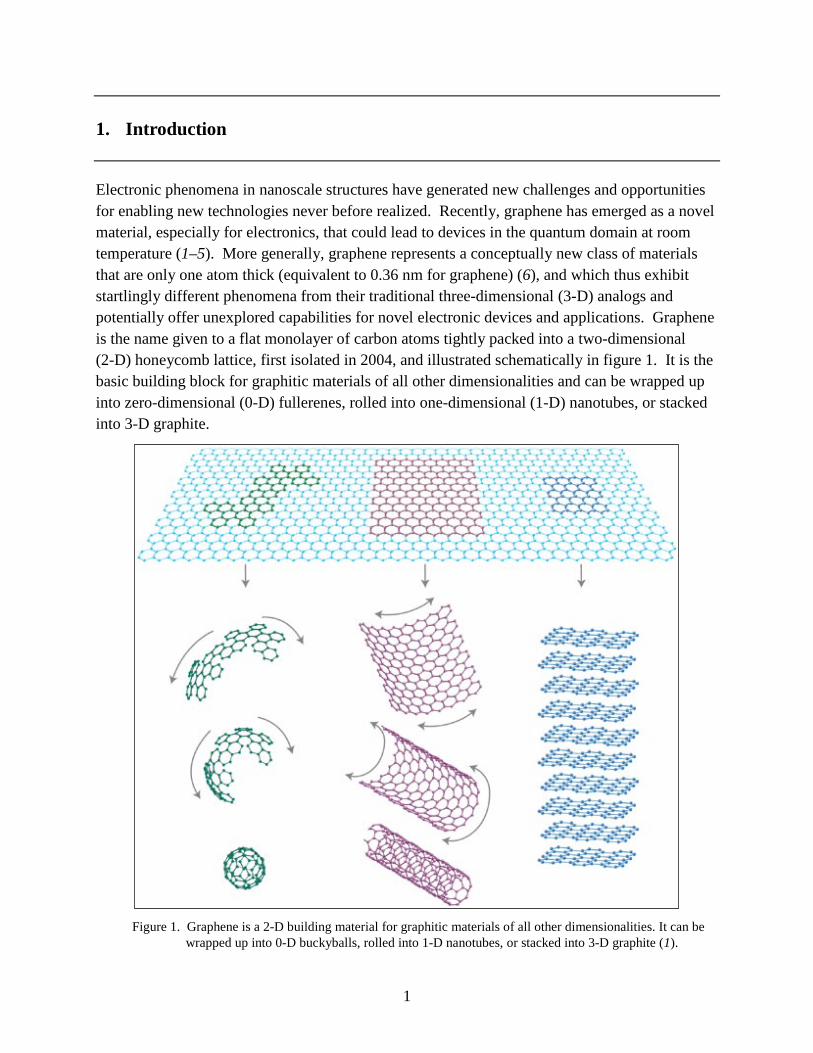
Electronic phenomena in nanoscale structures have generated new challenges and opportunities for enabling new technologies never before realized. Recently, graphene has emerged as a novel material, especially for electronics, that could lead to devices in the quantum domain at room temperature (1–5). More generally, graphene represents a conceptually new class of materials that are only one atom thick (equivalent to 0.36 nm for graphene) (6), and which thus exhibit startlingly different phenomena from their traditional three-dimensional (3-D) analogs and potentially offer unexplored capabilities for novel electronic devices and applications. Graphene is the name given to a flat monolayer of carbon atoms tightly packed into a two-dimensional (2-D) honeycomb lattice, first isolated in 2004, and illustrated schematically in figure 1. It is the basic building block for graphitic materials of all other dimensionalities and can be wrapped up into zero-dimensional (0-D) fullerenes, rolled into one-dimensional (1-D) nanotubes, or stacked into 3-D graphite.
Figure 1. Graphene is a 2-D building material for graphitic materials of all other dimensionalities. It can be
wrapped up into 0-D buckyballs, rolled into 1-D nanotubes, or stacked into 3-D graphite (1).

2
Graphene possesses a high electron and hole mobility with values shown as high as 200,000 cm2/V-s (7), a high thermal conductivity of ~5 x 10³ W/m-K (8), temperature stability to at least 2300 °C (but only ~500 °C in air [9]), extremely high tensile strength measured to be 1 TPa (10), quintessential flexibility, stretchability to 20% (11), a high breakdown current density exceeding 108 A/cm2 (12), and superior radiation hardness (13). All of these qualities are desired in electronic materials. In addition to these advantageous characteristics, graphene also possesses very unique ambipolar properties (capable of conducting electrons when biased in one direction and holes when biased in the other direction) that open up a whole new class of electronic devices.
Graphene lacks a bandgap in its energy band diagram, and therefore, exhibits metallic conductivity even at the limit of nominally zero carrier concentration. At the same time, most electronic applications rely on the presence of a gap between the valence and conduction bands. Several routes have been reported to induce and control such a gap in graphene. Some examples include using the effect of confined geometries such as quantum dots or nanoribbons, doping the edge states or the bulk of the graphene, applying a transverse electric field to a bilayer of graphene (14), and exploiting the proximity effects from an adjacent substrate or insulator layer. Current research shows that graphene’s atomic interaction with an epitaxial silicon carbide (SiC) substrate can induce a splitting of up to 0.3 eV between the maximum of the valence and minimum of the conduction bands at the Dirac point (15).
We at the U.S. Army Research Laboratory (ARL) are harnessing the electronic properties of this newly discovered material, and finding ways to develop and exploit a new generation of electronic and sensor devices for Army-specific applications. While many in the field are exfoliating micron-sized sections of graphene from chunks of graphite to study its fundamental physics or for measurements of unipolar complementary metal-oxide-semiconductor (CMOS)-like devices to extend Moore’s Law, our approach is to synthesize graphene using a manufacturable process, i.e., by chemical vapor deposition (CVD), and study a new class of graphene devices and circuits that harness the unique ambipolar properties of graphene. Such ambipolar devices and circuits hold the promise of more efficient and smaller analog circuits, increased frequency ranges, lower power consumption, and higher data transmission speeds, all in a transparent/invisible/durable/flexible form factor. This latter attribute could lead to wearable electronics woven into a Soldier’s uniform (so-called electronic textiles or “e-textiles”), for instance, for wireless communications or to sense health and medical condition. Medical sensors using graphene-based e-textiles, in turn, could be used to wirelessly transmit information to a central command node, trigger automated drug delivery (e.g., insulin), or be incorporated within “smart bandages,” which could accelerate healing of wounds. Many of the military advantages listed above could be also transitioned to civilian and commercial usages, which could make a large impact on the day-to-day world in which we live.
Further, as more sophisticated electronics are deployed to the battlefield, energy requirements become a greater burden on the Soldier. Exploiting the unique properties of graphene, we are

3
pursuing two avenues for solutions. First, as we have said, we are developing a new class of graphene-based nanoelectronic technology that would potentially replace larger, heavier, and power-hungry components in communications systems and portable electronics. Second, we are developing a new type of energy storage device called a supercapacitor, which uses graphene or carbon nanotubes (CNTs) and an electrolyte to produce ~100 times the specific power of batteries and fuel cells. Supercapacitors are capable of millions of charge/discharge cycles, rapid charge and discharge times, and high efficiencies. This research, in collaboration with Communications-Electronics Research Development and Engineering Center (CERDEC), aims to create a printable capacitor monolithically integrated with printable electronics to produce power for integrated electronic and sensor circuits.
In this first year of research under the ARL Director’s Strategic Initiative (DSI) program, we focused on developing in-house capabilities and infrastructures for producing electronic-grade graphene, characterizing its properties by a number of metrology tools, fabricating graphene test structures and graphene field-effect transistors (GFETs) incorporating a large variety of dielectric materials, testing these electronic structures and devices at direct current (DC) to radio frequency (RF) frequencies, exploring the use of graphene in supercapacitor devices for energy storage, and initiating efforts to model and simulate graphene device performance. Accordingly, the rest of this report is divided into the following sections:
• Section1: Introduction
• Section 2: Graphene Growth
• Section 3: Characterization
• Section 4: RF Top-gated CVD Field-effect Transistors (FETs)
• Section 5: Carbon Nanotube/Graphene Supercapacitors
• Section 6: Simulation and Modeling
• Section 7: Conclusions
1.1 Collaboration
We have established Cooperative Agreement with two universities that were executing strong programs on graphene and that had established capabilities and directions that were well aligned with our own goals. The first is the Massachusetts Institute of Technology (MIT)―Profs. Palacios (16, 17), Kong (18, 19), Jarillo-Herrero (20, 21), and Dresselhaus (22)―with significant progress in graphene-based ambipolar devices and circuits, as well as graphene growth by CVD and the production of suitable starting structures for device fabrication. The second is Rice University―Prof. Ajayan (23)―who has made exciting progress on some key building blocks for high performance graphene electronics, such as the co-synthesis of graphene with boron nitride (BN) (another purely 2-D monolayer and an excellent dielectric material for advanced
4
GFET devices) and the discovery of how to make graphene repetitively reconfigurable between semiconducting and insulating states. Collaborative arrangements have been established with both of these institutions to enhance our efforts, and these are reflected in the report. We are also working successfully with University of Texas, Austin, under Army Research Office (ARO)-funded 2-D materials and Stanford University using the ARL-funded Army High Performance Computing Research Center program. Collaboration with the Stevens Institute of Technology has also been established using an ARL-Defense Advanced Research Projects Agency (DARPA) ongoing agreement.
2. Graphene Growth
2.1 Chemical Vapor Deposition Furnaces
The capability to produce graphene thin films in-house at ARL is important to the success of the DSI. Epitaxial graphene growth on SiC has been the primary graphene growth technique for over five years; however, in recent years, CVD of graphene on metal substrates has shown great promise. CVD offers lower processing temperatures and cheaper substrate materials, and is considerably less difficult to set up in a laboratory setting than a high temperature furnace for graphene growth on SiC.
Two CVD furnaces were established for in-house graphene growth: an atmospheric pressure chemical vapor deposition (APCVD) furnace and a low pressure chemical vapor deposition (LPCVD) furnace. APCVD graphene growth was performed in the existing CNT furnace. Growth conditions for CNTs and graphene are very similar. Both use the same process gases: argon (Ar), hydrogen (H2), and methane (CH4). The major differences between CNT and graphene growth are the substrate materials and gas flows. As reported in the literature, CVD growth of single layer and bilayer graphene takes place at low methane flow rates (typically, 3–10 sccm) (18, 24). In order to accommodate the smaller flow rates, a new CH4 mass flow controller (MFC) was purchased and installed. The APCVD furnace was primarily used to growth graphene on nickel (Ni) thin films.
A new LPCVD furnace system was constructed at the Adelphi Laboratory Center (ALC), MD, this year. In hindsight, the purchase of a commercially established growth system may have been a prudent, albeit more costly, approach. It has been shown that single layer graphene, while difficult to produce using APCVD, can be produced under low pressure on copper (Cu) foils (25, 26). The key components to the system are the (1) gas delivery/handling system, (2) furnace, and (3) exhaust system. Located adjacent to the APCVD system, the LPCVD system is plumbed with the same gases as the APCVD system: H2, nitrogen (N2), Ar, CH4, ethylene (C2H4), and compressed air. The flammable gas flows are regulated using MFCs, while rotameters are used for the inert gases. The flammable and inert gases are kept in separate manifolds until they are

5
mixed right before entering the furnace. All valves on the system are pneumatically controlled and switched manually by an electronics panel. Once the gases reach the furnace, the gases enter a 2-in quartz tube heated by the furnace. The furnace can reach a maximum temperature of 1200 °C; however, it is typically operated at lower temperatures. The quartz tube and piping are evacuated by a mechanical roughing pump. A Baratron gauge downstream of the furnace measures the system pressure, and a butterfly throttle valve can be operated to set and control the pressure. The system can reach pressures as low as 250 mTorr. The LPCVD furnace has primarily been used for graphene growth on Cu foils.
2.2 Growth on Copper
2.2.1 Objectives
The overarching mission of the Graphene DSI is the development of fundamental electronic material/device theory and simulation, as well as synthesis and fabrication methods for discrete, coupled graphene-based devices specifically for power rectification and high frequency applications. While the primary focus is to develop graphene-based electronic devices and understand the fundamental behavior of these devices, in-house graphene synthesis is desirable to supply high grade material. As such, one challenge for this research is the deposition of high quality, large area graphene and the subsequent transfer onto device-compatible substrates. This year, the objectives were to (1) explore and optimize conditions for the low pressure CVD of single layer graphene on Cu foils, (2) improve the graphene transfer process and understand how the transfer process affects the physical properties of the graphene, and (3) characterize the graphene using Raman spectroscopy and atomic force microscopy (AFM).
2.2.2 Introduction
Graphene is a monolayer thick material comprised entirely of sp2-bonded carbon atoms that form a honeycomb-like lattice structure. Because it is only one atom thick, it is the prototypical 2-D material and as such exhibits unique physical properties. These interesting properties include a high intrinsic mobility (200,000 cm2/Vs) (7), a high breakdown current density exceeding 108 A/cm2 (12), and a constant optical absorption of 2.3% per layer over a wide spectral range (27). Graphene also possesses ambipolar behavior, which can potentially provide the foundation for new and previously unimagined devices. These properties make graphene an attractive material for many electronic applications, including transparent conductors, FETs, and frequency multipliers.
In this report, we discuss the activities performed during the second year of the Graphene DSI surrounding the growth and transfer of graphene deposited on Cu foils. Last year, one goal was to establish an in-house graphene growth capability via LPCVD. This year, various growth parameters were varied to deposit single layer graphene. However, primary emphasis was given to improving the graphene transfer process and understanding any transfer-related effects on the

6
physical properties of graphene. Growth, transfer, and characterization are all vital efforts to support the fabrication of graphene-based electrical devices.
2.2.3 Experimental Description
Graphene was grown by LPCVD on Cu foils with the goal of producing single layer graphene for device fabrication. Briefly, Cu foils were cleaned with acetic acid, acetone, and isopropanol and placed in a furnace. The furnace was pumped down to a base pressure of less than 0.5 Torr and then heated to the setpoint growth temperature under a constant flow of hydrogen gas. Once the setpoint temperature was achieved, the Cu foils were annealed in H2 for a set time. To initiate graphene growth, the growth pressure was set, and CH4 gas was then metered into the furnace with the H2. After the growth phase, the CH4 flow was stopped, and the furnace was cooled to room temperature. During the run, a thermocouple was inserted into the furnace to monitor the temperature, and it was found that the measured temperature was about 30 to 70 °C greater than the setpoint. A more detailed description of the deposition process can be found in reference 4. Over the year, growth parameters were varied, including temperature, gas flow rates, and deposition pressure. A listing of the various ranges can be found in table 1.
Table 1. Summary of the LPCVD graphene growth parameter ranges.
LPCVD Growth Parameters Pressure 1.5–9 Torr Temperature 900–1000 °C H2 flow rate 50–200 sccm CH4 flow rate 5–80 sccm Anneal time 15–30 min Growth time 5–40 min
A major effort this period was to optimize the transfer process of graphene from Cu thin foils to device-compatible substrates. The basic procedure has been outlined in the ARL Technical Report, ARL-TR-5451 (28). Briefly, a protective bilayer of poly(methyl methacrylate) (PMMA) is coated onto the graphene (on one side of the Cu foil). The unprotected backside graphene layer is removed using an oxygen plasma ash. Next, the Cu foil is wet chemically etched away, followed by a 10% hydrochloric acid (HCl) etch to remove any iron particulate residue from the Cu etchant. The remaining PMMA/graphene composite is transferred onto the desired substrate. Typically, a silicon (Si) substrate with 3000-Å-thick thermally grown silicon oxide (SiO2/Si) is used.
Two key steps in the transfer process are the oxygen plasma ash and the placement onto the desired substrate. Because of the Cu foil’s light weight and the heat/energy generated by the plasma, a method to secure the foil during this step is important to ensure that the foil does not flip during plasma processing. The previous method of using a water drop to adhere the Cu foil to a glass slide support was not sufficient to ensure adhesion during the entire plasma ash. Various methods were attempted to adhere the Cu foil to the support slide, including using

7
photoresist and other polymer-based materials as a glue. While these materials successfully kept the Cu foil fixed during the plasma ash, separation from the glass support and removal efforts further along in the process were problematic and prevented the use of these materials. Glass slides placed on the Cu foil edges provided the additional weight necessary to keep the foil stationary during the oxygen plasma ash. After Cu etching, the PMMA/graphene composite is transferred onto the desired substrate. Because a layer of water between the graphene and substrate exists, removing this water without disturbing or crumbling the graphene can be tricky. The previous method used a nitrogen blow gun to force the water from under the graphene. However, this method generated a number of failed transfers as blowing too hard or in the wrong place could cause the graphene to fold or move off the substrate. Instead, the samples were baked on a hot plate at ~50 °C to remove the water and adhere the graphene to the substrate. Using these two modifications, graphene areas greater than 1 in2 were successfully transferred. The yield for samples successfully transferred increased from 70% to 95% using these modifications.
The next phase of the transfer process is the removal of the PMMA handle layer. This removal was performed by two different techniques: acetone vaporization and thermal annealing. Acetone vaporization involves exposing the transferred graphene to heated acetone vapor, followed by submersion into boiling acetone. The second method involves heating the transferred graphene in a furnace at temperatures between 250–500 °C in a flow mixture of H2 and Ar at atmosphere. To determine the anneal conditions (i.e., temperature and gas flows) that best removes PMMA and explore any PMMA removal effects on the transferred graphene, a series of anneals were performed as described in table 2. Anneal time for each run was 90 min. As seen in table 2, the transferred graphene samples were either annealed or first had its PMMA layer removed by acetone vaporizations, followed by thermal annealing. The later was performed to separate thermal annealing effects from any potential unknown interactions between the graphene and PMMA upon annealing. There was some concern that the PMMA could possibly produce a carbonaceous residue on the graphene during annealing.
Table 2. Summary of the annealing experiment conditions for the removal of PMMA.
Temperature (°C)
H2 Flow (sccm)
Ar Flow (sccm)
Acetone vaporization 500 700 1700 Acetone vaporization 500 1700 500 500 700 500 500 1700 1700 Acetone vaporization 400 700 500 Acetone vaporization 400 1700 1700 400 700 1700 400 1700 500 Acetone vaporization 300 700 500 Acetone vaporization 300 1700 1700
300 700 1700 300 1700 500 250 1700 1700
8
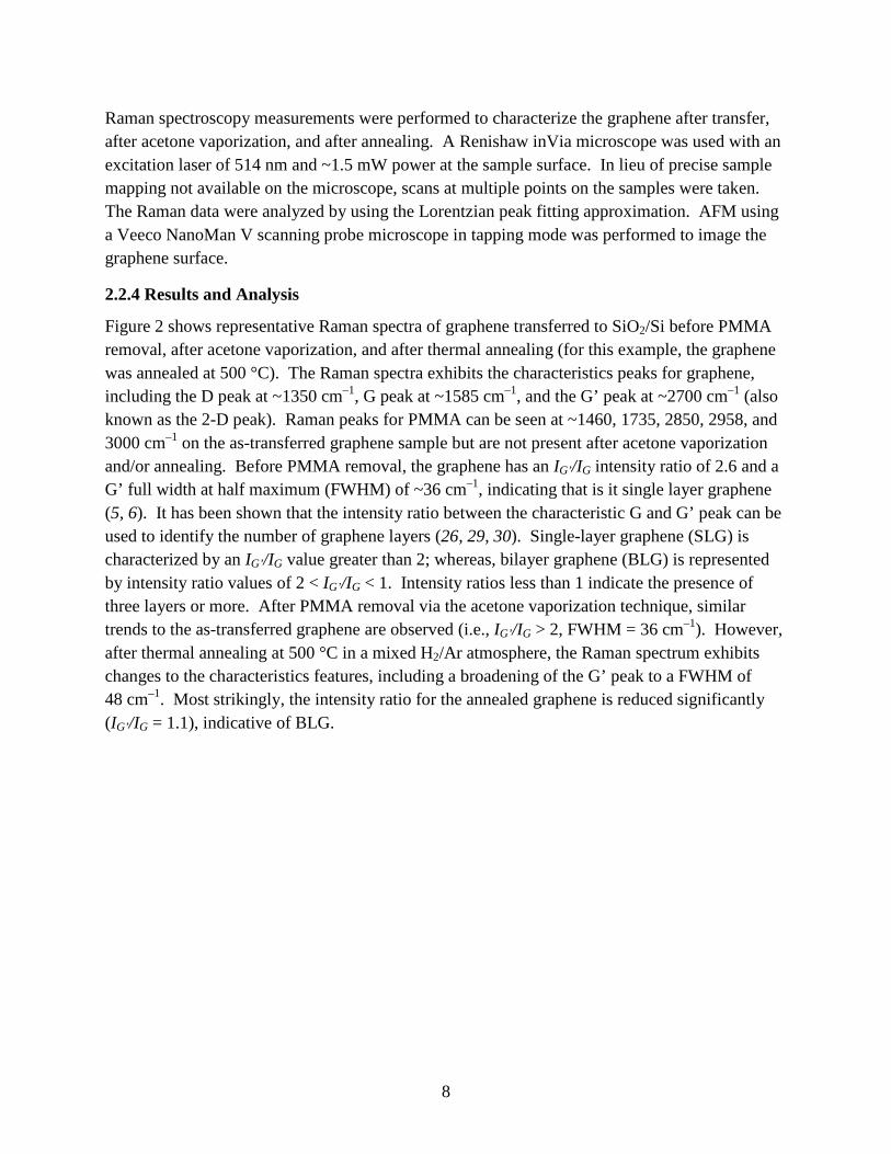
Raman spectroscopy measurements were performed to characterize the graphene after transfer, after acetone vaporization, and after annealing. A Renishaw inVia microscope was used with an excitation laser of 514 nm and ~1.5 mW power at the sample surface. In lieu of precise sample mapping not available on the microscope, scans at multiple points on the samples were taken. The Raman data were analyzed by using the Lorentzian peak fitting approximation. AFM using a Veeco NanoMan V scanning probe microscope in tapping mode was performed to image the graphene surface.
2.2.4 Results and Analysis
Figure 2 shows representative Raman spectra of graphene transferred to SiO2/Si before PMMA removal, after acetone vaporization, and after thermal annealing (for this example, the graphene was annealed at 500 °C). The Raman spectra exhibits the characteristics peaks for graphene, including the D peak at ~1350 cm–1, G peak at ~1585 cm–1, and the G’ peak at ~2700 cm–1 (also known as the 2-D peak). Raman peaks for PMMA can be seen at ~1460, 1735, 2850, 2958, and 3000 cm–1 on the as-transferred graphene sample but are not present after acetone vaporization and/or annealing. Before PMMA removal, the graphene has an IG’/IG intensity ratio of 2.6 and a G’ full width at half maximum (FWHM) of ~36 cm–1, indicating that is it single layer graphene (5, 6). It has been shown that the intensity ratio between the characteristic G and G’ peak can be used to identify the number of graphene layers (26, 29, 30). Single-layer graphene (SLG) is characterized by an IG’/IG value greater than 2; whereas, bilayer graphene (BLG) is represented by intensity ratio values of 2 < IG’/IG < 1. Intensity ratios less than 1 indicate the presence of three layers or more. After PMMA removal via the acetone vaporization technique, similar trends to the as-transferred graphene are observed (i.e., IG’/IG > 2, FWHM = 36 cm–1). However, after thermal annealing at 500 °C in a mixed H2/Ar atmosphere, the Raman spectrum exhibits changes to the characteristics features, including a broadening of the G’ peak to a FWHM of 48 cm–1. Most strikingly, the intensity ratio for the annealed graphene is reduced significantly (IG’/IG = 1.1), indicative of BLG.

9
Figure 2. Raman spectra comparison of graphene after transfer onto a SiO2/Si substrate, after acetone vaporization (ACE Vapor), and after thermal annealing at 500 °C.
AFM height images of the graphene surface topography after transfer, after acetone vaporization, and after thermal annealing can be seen in figure 3. The as-transferred sample contains the top PMMA protective layer (~1.5 μm thick) and thus no graphene features are visible in the image. More interesting is the comparison of the graphene surfaces after PMMA removal via thermal annealing and acetone vaporization. Both images exhibit root mean square surface roughness (σRMS) values of 1.4 to 1.6 nm. Wrinkles in the graphene can be seen in both images; however, there is a larger amount of debris, most likely residual PMMA, still present on the surface on the sample that experienced PMMA removal via acetone vaporization. The annealed graphene is much cleaner. It should also be noted that sizable rips and tears are typically visible in samples that undergo acetone vaporization as compared to annealed samples. These rips and tears in the graphene can be problematic when fabricating and testing electrical devices. Based on these results, it is preferable to use thermal annealing over acetone vaporization for PMMA removal.
1200 1600 2000 2400 2800 3200
Raman shift (cm-1)
Transferred
Inte
nsity
(a.u
.) ACE Vapor
D
AnnealedG'G

10
(a) As-transferred (b) After ACE vapor (c) Annealed
Figure 3. AFM height images of graphene (a) after transfer onto a SiO2/Si substrate, (b) after acetone vaporization (ACE vapor), and (c) after annealing at 300 °C.
The Raman spectra of four graphene samples annealed at 250, 300, 400, and 500 °C (furnace set point temperatures) in 1700 sccm H2/1700 sccm Ar can be seen in figure 4. As measured by thermocouple, the steady state temperature in the furnace was 50° higher than the setpoint temperature. For the sample annealed at 250 °C (actually 300 °C), the PMMA protective layer was not removed during the anneal. PMMA is known to fully degrade at about 360 °C in a nitrogen atmosphere; however, the degradation temperature decreases in the presence of oxygen as well as with increasing molecular weight of the polymer (31, 32). The PMMA layer is removed when annealed at setpoint temperatures of 300 °C or higher as expected.

11
Figure 4. Raman spectra of transferred graphene on SiO2/Si annealed at 250, 300, 400, and 500 °C.
One goal of the annealing experiment was to evaluate the effect of different H2:Ar flow ratios on the resulting physical properties of the graphene. Figure 5 shows the AFM height images of four graphene samples, annealed under varying H2/Ar flows at 300 °C. All images show wrinkles as expected. The images also show large raised features where multiple wrinkles gather and represent areas where the graphene is most probably not in contact with the SiO2/Si substrate. Roughness values range from 1.63 to 4.97 nm for these samples and are strongly influenced by the number of wrinkle gather features. Especially notable is the graphene sample annealed under 700 sccm H2/1700 sccm Ar (figure 5d). PMMA residue, usually revealed as small circular particles bunched together, is observed in the graphene annealed under 700/500 sccm H2/Ar (figure 5b). For these four samples, no discernible difference in the Raman spectra has been observed. Therefore, it can be concluded that temperature, not the anneal gas flow environment, plays a dominant role in influencing the chemical/structural properties of graphene. There have been many reported thermal annealing recipes that purport to remove PMMA from graphene, including annealing in vacuum (33–36). However, the main similarity among them has been the use of elevated temperatures, ranging from 300 to 500 °C, which is necessary for the sublimation of PMMA.
1500 2000 2500 3000
500 deg C 400 deg C 300 deg C 250 deg C
Inte
nsity
(a.u
.)
Raman Shift (cm-1)

12
(a) H2/Ar: 1700/1700 sccm (b) H2/Ar: 700/500 sccm
(c) H2/Ar: 1700/500 sccm (d) H2/Ar: 700/1700 sccm
Figure 5. AFM height images of transferred graphene annealed at 300 °C under various gas flows: (a) 1700 sccm H2/1700 sccm Ar, (b) 700 sccm H2/500 sccm Ar, (c) 1700 sccm H2/500 sccm Ar, and (d) 700 sccm H2/1700 sccm Ar.
The influence thermal annealing has on the graphene Raman spectra is visible when comparing the intensity ratios values. Figure 6 plots the intensity ratio IG’/IG for the transferred graphene before and after PMMA removal. The as-transferred graphene samples exhibited IG’/IG values greater than 1, indicating that they consist of single and bilayer graphene. Calculations from the Raman spectra of each sample suggest they are 77–100% SLG and 0–23% BLG. The average intensity value for all transferred graphene is 2.04. Graphene that had PMMA removed via the acetone vaporization process exhibited an average IG’/IG of 2.21 with a tight distribution around 2. These graphene samples exhibited 85–100% SLG. Graphene annealed at 300 °C or higher, regardless of whether it had the PMMA removed previously or not, did not exhibit any characteristics of single layer graphene. The average IG’/IG value for these samples is 1.11. No correlation between anneal temperature and IG’/IG ratio values was observed.

13
Figure 6. IG’/IG values for graphene after transfer, after acetone vaporization (ACE Vapor), and after thermal annealing at 300 to 500 °C.
The intensity ratio IG’/IG was not the only change seen with the Raman spectra; shifts in the G and G’ peak positions has also been observed. Table 3 shows the mean position for both peaks with respect to PMMA removal method. The most dramatic change occurred for the G peak. For the transferred graphene, the mean G peak position was 1591.1 cm–1; however, after acetone vaporization, the mean position shifts by –4.3 cm–1. An increase in the mean G peak position from 1589.9 to 1597.1 cm–1 is observed as the annealing temperature increases from 250 to 500 °C. A similar trend is also observed in the G’ peak position, although not as large. Again, there is a slight decrease from the as-transferred to the PMMA removal via acetone vaporization and a slight increase as the annealing temperature is increased.
Table 3. Summary of the Raman G and G’ peak position after transfer, after acetone vaporization, and after annealing from 250 to 500 °C.
G Peak Position (Mean) (cm–1)
G’ Peak Position (Mean) (cm–1)
Transferred 1591.1 2691.4 Acetone vaporization 1586.8 2689.8 Annealed at 250 °C 1589.8 2696.2 Annealed at 300 °C 1592.3 2694.6 Annealed at 400 °C 1596.3 2694.7 Annealed at 500 °C 1597.1 2696.6
2670 2680 2690 2700 27100
1
2
3
4
5
Transferred ACE Vapor Annealed
I G' /I
G
G' Peak Position (cm-1)

14
Similar changes in the Raman spectra as a function of anneal temperature have been observed in exfoliated graphene (33, 34). A decrease in the IG’/IG value from above 1 for pristine SLG to 0.5 after annealing was observed in exfoliated SLG as the samples were annealed at progressively higher anneal temperature (250 and 400 °C) (34). G peak position shifts as large as 20 cm–1 were also reported upon annealing at 400 °C. It is believed that the shifts in Raman peak position and changes in the intensity are due to increased interaction or coupling of the graphene layer and the underlying SiO2/Si substrate, which in turn leads to heavy hole doping and severe degradation of the electrical properties in graphene devices. It is thought that the silicon oxide contributes excess charge to the graphene and is responsible for hole doping in graphene samples.
2.2.5 Conclusion/Summary
This section of the report described research done under the Graphene DSI focusing on the growth, transfer, and characterization of graphene deposited on Cu foils by LPCVD. Efforts to optimize the graphene transfer process were discussed, including the experiments performed to explore how the PMMA removal impacts the physical properties. PMMA removal methods of acetone vaporization and thermal annealing were compared. While thermal annealing is preferred over acetone vaporization because of the rips and tears generated in the later, exposing the graphene to elevated temperatures changes the physical properties. Upon transfer, the graphene are typically composed of 77–100% SLG and 0–23% BLG; however, upon annealing, Raman spectra indicate that the samples no longer contain any SLG material. This effect is most likely not due the presence of carbonaceous material left over from the PMMA removal process, but rather due to increased coupling of the graphene and substrate brought on by heating.
2.2.6 Future Work
Based on the work performed during this year, several areas of research have been identified that warrant future investigation. While this year’s growth efforts have focused on determining conditions for SLG, the next steps forward will focus on increasing the grain size of graphene. This should entail varying the growth conditions, especially the hydrogen partial pressure, which has been shown to influence grain size (37), as well as exploring pre-growth treatments of the Cu foil (FY12 Q1–4). This year’s work has shown that the cleaning process for the transferred graphene remains a notable issue. Particularly, PMMA removal is still problematic and investigation into alternative cleaning solvents and process should be continued (FY12 Q2–4). The influence of these solvents on the structural properties of the graphene must be considered in addition to understanding and differentiation of the graphene-substrate effects from PMMA removal effects. Another goal for the upcoming year is to develop and perform electrical measurements, such as sheet resistance and/or Hall measurements, for pre-fabrication electrical characterization and assessment of the graphene (FYQ3).

15
2.3 Growth on Nickel
2.3.1 Introduction
Graphene growth can be synthesized and controlled on metal surfaces by APCVD. The challenge has been controlling the number and area of the grown G-layers on metals. Ni and Cu are affordable, readily available metals in semiconductor industry and have a particularly low carbon solubility (~1%). Carbon is needed in the process for growing graphene. The advantage of APCVD method is in the ability to transfer the G-layers to a flexible substrate for continuation in the electronic device fabrication.
Ni foil has been a very popular form of starting material for graphene transparent conductive electrodes (38), but the requirements for GFET device application are more stringent in terms of atomic smoothness, low defects, low roughness, and high electronic mobility for high performance. The structural quality of Ni is of immense importance both in improving growth procedures and understanding the resulting G-layers electronic properties. Multilayer graphene prepared by diluted CH4-based CVD at 1 atm on Ni films deposited over Si/SiO2 wafers has been shown in various colors, sizes, and shapes (39). Their preferred nucleation sites in relation to the Ni grain boundaries are not well understood. In this study, we prepared a variety of Ni catalysts having grain structures ranging from small to large and with mixed distribution across the surface.
We have also significantly diluted the mixture of CH4, a carbon source in the APCVD process, to less than generally found 2‒16 vol.% (39–43). Other studies using less than 2 vol.% (18, 44, 45) have shown diluted CH4 was key to the growth of SLG and BLG and few-layer graphene (FLG) (less than five layers), while using concentrated CH4 led to the growth of multilayer graphene that resembled bulk graphite. We employed diluted amounts equal to and below 0.5 vol.% to obtain nanolayers of graphene.
2.3.2 Experimental Procedure
The process for synthesis of graphene film started with Ni coated on SiO2/Si substrates. The Ni film was deposited by evaporation or sputtering to a thickness of 300 nm. The sputtering was performed at a temperature of 100 and 250 °C each with a pressure of 2 and 20 mT. The substrate was then loaded into a CVD furnace and the temperature was ramped up as fast as possible to 950–975 °C. The annealing process was carried out at atmosphere with H2 flow rate of between 300 to 700 sccm, and the Ar was held constant at 700 sccm. At the start of the graphene step, we started flowing 5 sccm of CH4 as a carbon source for approximately 10 min. After the growth step, we turned off the CH4 and ramp down the temperature of the furnace at a rate of 5 °C/min while maintaining the same flow rates of H2 and Ar. The Ni and graphene film morphology were analyzed using the high-resolution nanoscale imaging technique of AFM; a Veeco NanoScope V on the contact mode focused over an approximately 2-µm2 sample surface. The quality of graphene was analyzed by micro-Raman spectroscopy. All scans were taken on

16
Witec Alpha 300 instrument run in Raman mode with a 532-nm excitation laser (laser power less than 45 mW), a 600 l/mm diffraction grating, and a 60 × 0.8-NA objective lens.
2.3.3 Ni Film Preparation
A direct comparison of the Ni film preparation and deposition methods reveals changing grain structures ranging from small to large and with mixed distribution across the surface.
The film from the evaporation method has a grain size is approximately 45 nm and equilateral with an average roughness value Ra of 8.7 nm. The grain distribution is mostly equal all around. Evaporated and sputtered thin films deposited in a condition of supersaturation typically result in small grain sizes due to a high rate of nucleation (46). Film from the sputtering method at temperature (100 °C) and low pressure (2 mT) have grains that grow to approximately 90 nm in size with an Ra of 9.3 nm. Sputtering above ambient temperature produces a larger grain size and more defined grain boundaries than evaporated grains, as shown in figure 7a and 7b. The distribution is 30% occupancy of large grains. An increase in sputtering pressure to 20 mT tends to reduce the grain size to approximately 80 nm and reduce the occupancy to 50% large grains, as shown in figure 7c. We note the sputter deposition rate is only 43 nm/min at 20 mT, almost half that deposited at 2 mT. At 20 mT, sputtering there is a reduction in free mean path of Ar atoms to the Ni target, which produces increased collisions that slow down the deposition rate. An increase in the sputter temperature to 250 °C produces noticeably larger grains of roughly 600 nm in size with a Ra of 27 nm, as shown in figure 7d. At this temperature, there is evidence of grain growth and formation of large flat plateaus from topographical features.
Figure 7. AFM image of Ni morphology before CVD growth of graphene by method of (a) evaporation, (b) sputtering 2 mT, 100 °C, (c) sputtering 20 mT, 100 °C, and (d) sputtering 2 mT, 250 °C.
2.3.4 Ni Annealing
Annealing is necessary for grain growth and the stability of the film. After 20 min of annealing at 975 °C, the average grain size increase to several times its original size. If we compare how the grain evolves from their original size in figure 7a–c and their corresponding annealed state figure 8a–c, we find the distribution remains nearly the same mix. That is, the proportion of small grains and large grains are relatively the same. In evaporated films, the grains continue to be equilateral and grow to an average size of 2000 nm, which is an approximately 50 times increase from their original deposited condition.

17
Figure 8. Morphology of (a) equilateral grains from evaporation; (b) 30% large grain from sputtering, 2 mT and 100 °C; and (c) 50% large grains from sputtering, 20 mT and 100 °C.
The sputter deposited grains reach a maximum 10,000 nm in size, nearly 11 times their original size. Other investigators have shown on average a 20-times increase in growth (47). The large grains occupy 30% of the surface when sputtering pressure is held at 2 mT, but occupy 50% when the pressure is 20 mT. The effect of increasing the sputter pressure was to suppress the nucleation of small grains around larger grains.
The results for sputtered film at temperature elevation of 250 °C (figure 7d) are not shown here, but for 450 °C the final grain size is said to approach 25 µm after the annealing stage (24). Grain growth will stagnate in thin films during annealing at some point according to the film thickness. The ratio of the annealed grain diameter to that of the Ni film is generally said to be around 20, which could only be obtained by abnormal grain growth (48). Normal grain growth rarely occurs in thin films. An important characteristic of the normal grain growth is that, after the annealing, the average grain size does not exceed the original film thickness. The shape and grain size distribution of the single grain does not change. Abnormal grain growth is preferred because the average grain size can be up to an order of magnitude larger than the original film’s thickness. Others have shown greater than normal Ni grain diameter growth to 50 µm by exposing the film to a pressurized vessel of 200 Torr at 1000 °C and extending the annealing time from 20 to 60 min (44), but there was no mention of the quality of surface roughness resulting from this process.
2.3.5 Role of H2 in the APCVD Process
The H2 environment plays an important role in preventing oxidation of Ni at high temperature. The quality of the film has been shown to improve with the addition of H2 (49). The likely explanation for this is that H2 is known to selectively etch amorphous carbon defects that can serve as secondary nuclei for competing film growth. It can also cause problems to thin-film Ni and other metals over time or if the content is too high, in a phenomenon called hydrogen blistering (24). A pinhole is shown in figure 3 in the form of a tiny black hole, which can vary in size and density with the amount of H2 flow in the process. At elevated temperatures, hydrogen atoms are able to diffuse into Ni and accumulate in clusters until the pressure builds up to the point of bursting. Reducing the amount of H2 during the annealing stage is important in preventing pinholes in very thin Ni films.

18
The amount of H2 flow was optimized to 30 vol.% in order to prevent oxidation and pinhole defects. Oxidation is characterized by darkening and roughening of the Ni surface with missing layers of graphene. We found that less H2 was needed when the grains of Ni were larger in order to obtain consistent and reliable growth of graphene. This conclusion was arrived coincidentally after many trials attempting to find an optimum H2 flow setting. Beyond this amount, the pinhole defect density count increased astronomically with increase in H2content as shown in figure 9.
Figure 9. Excess H2 leads to pinholes in Ni catalyst.
On a very thick Ni film (0.5 mm), the amount of time needed for successful annealing for growth of graphene (50) was 1 h, but there was no mention of the post surface roughness and pinhole conditions.
2.3.6 Graphene Growth
A source of carbon in the CVD process that is necessary for the growth of graphene on top of the Ni catalyst is a reaction product from gas mixture of H2 and CH4 at 975 °C in atmospheric conditions (51). Since the solubility of carbon in Ni is temperature-dependent, carbon atoms segregate as a graphene layer on the Ni surface upon cooling. Others (52) have used thin Ni films (700 nm, deposited by sputtering on SiO2/Si wafer) rather than thick Ni foil (0.5 mm) to minimize the saturation time and the amount of carbon in the Ni film, since the solubility of

19
carbon in Ni is about 0.9 at.% at 900 °C. For other materials, like Cu, the carbon solubility is negligible and the substrate can reach a substrate thickness of 25 μm. For Ni, we used a thin-film layer of 300 nm.
A CH4 ratio from 0.5 to 0.41 vol.% exhibited a strong presence of graphene film, at 0.36 vol.% produced mixed results, and at 0.24 vol.% or less produced no evidence of graphene on a Ni catalyst after CVD. We were successful in growing graphene with mixed results below dilution (0.36 vol.%) by extending the CVD growth time to 10 min from the previous 5 min (44). It is expected that conditions such as annealing time, temperature, and H2 content will shift these results.
Finding evidence of graphene growth can sometimes be challenging when using a microscope. SLG or BLG are transparent (39), but multiple layers of crystallites are opaque and can be visualized using optical microscopy. Visual detection of SLG and BLG is improved by transferred graphene to any 300-nm-thick SiO2 substrate and using monochromatic illumination (53). The apparent transparency of 1‒2 layer graphene grown over the Ni catalyst is beneficial for determining the background surfaces. The morphology and grains of the Ni are discernible in figure 10. The faint black lines in the background are the Ni grain boundaries and the graphene patches in brown color represent several layers. The grain boundaries of Ni at the CVD stage take on the same fingerprint characteristics as compared to the annealing stage.
Figure 10. Distribution of graphene patches on top of (a) evaporated Ni with equilateral grains; (b) occupancy 30% large grains from sputtered, 2 mT and 100 °C; and (c) occupancy 50% large grains from sputtered, 20 mT and 100 °C deposit conditions.
Inspection of the grain boundaries after graphene growth reveals the preferred nucleation sites of multilayer graphene patches. In figure 10a, graphene patches measuring approximately 10 µm across appear to cover several smaller grains of Ni prepared by evaporation method. When a Ni grain diameter is relatively large from a sputter preparation method, as depicted in figure 10b, the graphene patches prefer to grow in concentrated areas of small Ni grain boundaries and are less likely to appear on top as single large flat areas. There is a higher density of atomic steps due to the curvature of the grain edge, thereby inducing the nucleation sites of graphene patches (39, 47). In areas depicting large equilateral grain size with fewer grain boundaries, such as in figure 10c, the quantity of graphene patches appears to remain relatively unchanged compared to figure 10a. It appears that long length grain boundaries can have few nucleation sites, and on the other hand, short length grain boundaries can have many nucleation sites. If multilayer graphene

20
originates at the grain boundaries, as in seen in both figure 10a–b, then hypothetically the large numbers of grain boundaries in figure 10a should be completely covered of multilayer graphene patches. One possible reason for the few nucleated multi-graphene sites on overwhelming numbers of Ni grains boundaries is that the individual grains have a (111), (100), and possibly more crystallographic orientation (42). In face-centered cubic (fcc) metals such as Ni, the (111) planes have their lowest surface/interface energy with respect to other planes (46) and growth is preferred in those planes. However, in Ni films that have high stress, the surface/interface energy minimization is no longer the dominant driving force. Ni grains growth is preferred with a (100) crystallographic orientation because Young’s modulus allows the grains to expand and contract in those planes much more easily in order to reduce the internal stress. Usually high quality epitaxial grown graphene is associated with the smallest lattice mismatch, but this tendency needs to be studied further before making a concrete determination. The driving force or nucleation sites of multilayer graphene patches are not strongly dependent on grain size when using diluted CH4 concentrations below 0.5 vol.%.
A stronger influence of the quality and quantity of graphene is dictated by the effect of temperature and the rate of cooling at diluted amounts of CH4. Other studies have shown a moderate cooling rate provides the best conditions for graphene growth (18). At moderate cooling rate, carbon atoms segregate and form graphene; while at a higher rate, carbon atoms segregate out of Ni, but form a less crystalline, defective graphitic structure (54). Others have used very fast cooling rates of 10 °C/s successfully, but these conditions were done with either thicker films or higher concentration (5‒16 vol.%) of CH4 (39–41) and high (400 Torr) pressure (42). We chose a slow cooling rate of 5 °C/min for our thin-film Ni and a dilute CH4 concentration.
The CVD temperature also has a strong influence on the graphene patch size. We lowered the process temperature to 950 °C to determine the change in graphene patch size. When the temperature was reduced by 25 °C from the original condition (figure 11a), the graphene patches were reduced to nearly half the size (figure 11b) for the evaporated sample. The largest size graphene patch at 975 °C measured 20 µm across for a 300-nm-thick Ni film.
Figure 11. Size comparison of multilayer graphene patches grown and annealed at (a) 975 °C and (b) 950 °C from an evaporated Ni template.

21
2.3.7 Raman Spectroscopy
The amount of graphene layers segregated on the Ni catalyst surface after CVD growth can be characterized by Raman intensity peaks. Figure 12 shows a comparison of graphene grown patches on the Ni surface ranging from light to dark shades of green.
Figure 12. Comparison of images according to (a) clear or transparent, (b) light, (c) medium, and (d) dark graphene patches on evaporated Ni surface.
Micro-Raman spectroscope was positioned at the crosshair locations corresponding to those same images and the intensity peaks are recorded in figure 13.
Figure 13. Comparison of Raman intensity peaks according to (a) clear or transparent, (b) light, (c) medium, and (d) dark graphene patches on Ni.
Raman bands at 1580 to 1584 cm–1 and 2711 to 2713 cm–1 are denoted as the G band and 2D band, respectively (55). The 2D band is also denoted as G’ band. Differences among the Raman spectra were observed, including an increase of the G band to 2D band intensity ratio and a broadening of the 2D band. The G band originates from in-plane vibration of sp2-hybridized carbon atoms and generally becomes stronger with an increasing number of layers, for layers

22
typically smaller than 10. The 2D band becomes broader and shifts toward a higher wave number with increased graphene layers due to a splitting of the electronic band structure. Figure 13 shows Raman spectra of different number of graphene layers, exhibiting the G and 2D modes. The intensity ratio of G to 2D modes increases with the number of graphene layers.
SLG typically has a sharp and symmetric 2D band at 2683 cm–1 depending on the background substrate (56, 57), but we see no evidence of this in the chart. Where two or more layers of graphene exist, the shape of the 2D mode evolves significantly. The 2D mode in bulk highly ordered pyrolytic graphite (HOPG) generally can be resolved into two components, 2D1 and 2D2, where as SLG has a single sharp component (58). Single 2D component, monolayer, and four components in bilayer have been explained in terms of double resonance Raman scattering (59). The 2D1 component is less intense than the 2D2 component; whereas, for the BLG these bands have almost the same intensity. An increase in number of layers leads to an incremental increase of the higher frequency 2D2 component compared to the 2D1 component. These characteristics of a bilayer are present in figure 6a with broadening of the 2D band centralizing near 2700 cm–1 and the I(G)/I(2D) ratio near unity. The Lorentzian 2D curve is symmetrical, although missing is a typical hump on the left-hand side, normally associated with two-layer graphene (60). Multilayer graphene exists when the I(G)/I(2D) ratio increases in the range above two layers with the broad shape of the 2D mode becoming asymmetrical and shifting to higher wave numbers, as shown in figure 12b–d. Very similar low resolution spectra are confirmed on graphene layers after the graphene was transferred to an insulating substrate (61).
The intensity of the G band increases almost linearly as the graphene thickness increases (56). All the layers show activity at the 1340 cm–1, also known as the D band, which relates to the occurrence of defects and disorder in the crystal. The disorder-induced D bands at the 1355 cm–1 became distinct for thinner graphene films, a reflection of how defects can be easily be incorporated into thinner graphene sheets (55). The relative intensity of an existing D band decreasing to less than 10% of the G band with increasing crystallite graphene layers is comparable to high-quality graphene films grown by CVD (62).
2.3.8 Conclusions
Multilayer graphene patches are not dependent on the grain size of the Ni catalyst when the diluted CH4 concentration is below 0.5 vol.%. This was demonstrated by growing graphene on Ni films prepared with a variety of grain sizes. Multilayer graphene patches were distributed equally onto the surface regardless of changing grain sizes. The surface area of graphene is comprised of approximately 20% tri-layer with remaining multilayer patches. The process temperature had a strong influence on the size of graphene patches. A 25 °C change in CVD temperature can be used to change the size of multilayer graphene by almost a factor of two, particularly on evaporated Ni. Annealing at the highest possible temperature and combine it with an appropriate cooling rate results in the largest possible multilayer graphene patch size.

23
2.3.9 Summary
We achieved tri-layer graphene on sputtered and evaporated Ni catalyst based on Micro-Raman analysis:
• Graphene layers are very dependent on CH4 gas concentration.
• CH4 0.5–0.4 vol.% exhibited graphene multilayers >4.
• CH4 0.4–0.3 vol.% exhibited evidence tri-layer growth in 20% area.
• Graphene layers are not dependent on the Ni grain size alone because same size layers were found in both large and small Ni grains.
The Ni catalyst can oxidize or form pitting defects:
• Controlling H2 is essential to preventing oxidation in 1000 °C APCVD process.
• <30 vol.% produces oxidation.
• >50 vol.% causes pitting defects.
Starting material grain size may have an influence in the annealing process:
• Initial analysis shows that larger Ni grains needed less H2 to prevent oxidation.
2.3.10 Proposed Work FY12
We propose to accomplish the following in FY12:
• Reduce the number of graphene layers from three to two.
• Improve coverage area of BLG to greater than 50% for device quality fabrication.
• Introduce high temperature sputtering (>300 °C) to increase the Ni grain size (contract with Thin Film, Inc., NJ).
• Use high temperature spiking annealing technique to increase Ni grain size (collaboration with Dr. Jing Kong at MIT).
• Perform x-ray diffraction (XRD) of high temperature prepared Ni and annealing conditions to determine preferred crystal orientation and relationship to number of G-layers.
• Improve the G transfer process to reduce residues.

24
3. Characterization by Raman Spectroscopy
3.1 Introduction
Graphene is a single, one-atom-thick, sheet of carbon arrange in a honeycomb lattice, and as such is a true nanomaterial that is effectively all surface (63, 64). Therefore, to ascertain graphene’s intrinsic properties one needs a metrology that will provide atomic-level structural, chemical, and topological information such as layer stacking sequence, crystalline quality, and number of atomic layers. Such information is required by the device fabrication engineer so that judicial decisions can be made during the fabrication process of graphene-based nanoscale devices and sensors. Raman and AFM are non-destructive techniques used extensively to investigate these materials properties for carbon-based nanomaterials such as graphene. It is the former technique (i.e., Raman) that is the main topic of this section of the report.
3.2 Theory and Concept
3.2.1 Optical Properties
There are a number of different ways in which photons can interact with excitations inside a material. They can interact through quantized lattice vibrations (phonons), free electrons and holes, impurities and defects, and ionization processes (65). Figure 14 (adopted from [66]) shows schematically some of the optical processes that can occur when light is incident upon a material; in this case, a semiconductor. A fraction of the light is reflected at the air/semiconductor interface, while the remainder is transmitted into the material. Inside the semiconducting sample, some of the light may be absorbed or scattered while the rest is transmitted completely through the semiconductor. In general, the strongest optical processes are reflection and photon absorption via electron-hole creation, because they involve the lowest order of interaction between incident light and the elementary excitations inside the material. Some of the absorbed radiation may be reemitted at a different frequency, a process known as photoluminescence. Scattering processes such as Brillouin and Raman scattering involve two interactions (since there is incident light and scattered light), and therefore, tends to be much weaker (66). It is the later of these scattering processes—Raman scattering—that is relevant to this discussion.

25
Figure 14. Schematic diagram illustrating the linear optical processes that occur at the surface and in the interior of a semiconductor.
3.2.2 Phonons
A basic understanding of phonons is useful when developing a physical understanding of the Raman scattering process. Therefore, a short and simple review of phonons and their dispersion is given here. This derivation can be found in most introductory solid-state physics texts (67–69).
To obtain some insight about the properties of phonons, we show how the energy of a phonon depends on its wave vector (i.e., its dispersion) for a simple system. Consider the linear-chain model of figure 15. This model represents a hypothetical linear crystal with two atoms per unit cell of lattice constant a. The larger atom has a mass M and the smaller m, and we assume that they only interact with their nearest neighbors. The spring constant of the connecting springs are all the same and labeled K. Introducing the displacement in the nth unit cell of M as un and that of m as vn we obtain
𝑀𝑑2𝑢𝑛𝑑𝑡2
= 𝐾(𝑣𝑛 + 𝑣𝑛−1 − 2𝑢𝑛) (1)
and
𝑚𝑑2𝑣𝑛𝑑𝑡2
= 𝐾(𝑢𝑛+1 + 𝑢𝑛 − 2𝑣𝑛) (2)
using Newton’s 2nd law of motion and Hooke’s law of a mass attached to a spring.
Figure 15. One-dimensional diatomic chain with lattice constant a.

26
As solutions of equations 3 and 4, we try plane waves with amplitudes of u and 𝑣, in this case,
𝑢𝑛 = 𝑢 exp[𝑖( Ω𝑡 + 𝑛𝑄𝑎)] (3)
and
𝑣𝑛 = 𝑣 𝑒𝑥𝑝[𝑖( Ω𝑡 + 𝑛𝑄𝑎)] (4)
where Q is the phonon wavevector and Ω is its frequency. Substituting equations 3 and 4 into equations 1 and 2, respectively, we obtain
− Ω2𝑀𝑢 = 𝐾𝑣[1 + 𝑒𝑥𝑝(−𝑖𝑄𝑎)] − 2𝐾𝑢
(5) − Ω2𝑚𝑣 = 𝐾𝑢[1 + 𝑒𝑥𝑝(𝑖𝑄𝑎)] − 2𝐾𝑣.
This set of equations has a nontrivial solution (i.e., one other than u = v = 0) only if the determinant of the coefficients vanishes. That is,
2𝐾 − Ω2𝑀 −𝐾[1 + 𝑒𝑥𝑝(−𝑖𝑄𝑎)]
−𝐾[1 + 𝑒𝑥𝑝(𝑖𝑄𝑎)] 2𝐾 − Ω2𝑚 = 0 (6)
The dispersion relation resulting from the corresponding secular equation can be written as
Ω4 − 2𝐾Ω2 1𝑀
+1𝑚 +
2𝐾2
𝑀𝑚(1 − 𝑐𝑜𝑠𝑄𝑎) = 0 (7)
Equation 7 can be solved exactly and the solutions are plotted in figure 16 for positive Q’s in the first Brillouin zone (BZ). The lower branch is called the acoustic branch since sound waves propagate according to its modes, and the upper branch is called the optical branch. The two different atoms are displaced in the same direction for the acoustic branch and only the heavy masses oscillate at the edge of the BZ. The Q = 0 case (i.e., for an infinite wavelength) of the acoustical branch corresponds to a simple displacement of the whole crystal. For the optical branch, the two atoms are displaced in opposite directions and only the light masses oscillate at the edge of the BZ. The Q = 0 case for the optical branch corresponds to an equal displacement of each like atom from its equilibrium position. When Q = 0, the vibrational mode is known as the zone center phonon. If the bonds between the atoms have some ionicity, the two different atoms carry an electric charge, and hence, the anti-phase oscillation (optical) is connected with an oscillating electric dipole. This allows a coupling to the electromagnetic field and is the reason why these oscillations are called optical modes.

27
Figure 16. The dispersion relation for the 1-D diatomic chain.
3.2.3 Raman Scattering
As was mentioned in section 3.2.1, most light that is incident on a semiconductor is reflected, transmitted, or absorbed. However, a very small number of photons are scattered by inhomogeneities inside the medium. These inhomogeneities may be static or dynamic. Static inhomogeneities are purely geometric or local with no time dependence and results in elastic scattering of the incident photons, i.e., without a frequency change. Defects such as dislocations in a crystal are static scatters. On the other hand, dynamic inhomogeneities are time-dependent and result in inelastic scattering processes that do involve a frequency change. Phonons (a quantum of lattice vibration) in a solid are an example of a dynamic scatter. Dynamic scatterers lead to the formation of sidebands to the excitation line, as in Brillouin (70) and Raman (71) scattering. Valuable information on the vibrational states of the material can be obtained from these experiments (66, p. 362). In this study, we are primarily concerned with the Raman response due to inelastic scattering by optical phonons.
Raman scattering has proven to be an extremely useful method for the characterization of semiconductors (66, 72, 73). Raman scattering results when photons interact with optical phonons, and therefore, complements the other spectroscopic techniques used in this study, which are functions of the electronic states of the semiconductor. Phonons are very sensitive to their local environments. The way in which the phonon frequencies appear in a Raman spectrum can give information about crystal quality and strain effects, which change the semiconductor’s lattice structure and, in turn, alter the phonon frequency of the material. The Raman scattering

28
intensity for a given phonon mode is also a function of the sample orientation with respect to the polarization of the incident and scattered radiation, i.e., selection rules for Raman scattering exist that are related to the geometry of the crystal. Therefore, Raman scattering can be used to determine both the frequency and symmetry of a phonon mode (66, p. 366).
3.2.4 Macroscopic Theory of Raman Scattering
A complete theory of Raman scattering is very complex. Unlike some other spectroscopy techniques, a comprehensive line-shape analysis is not often used for Raman spectroscopy due to the complex theoretical problems involved. Even though a simplified quantum-mechanical theory of Raman scattering (74, p. 183) can yield many of the important parts of a complete theory, we feel that a simple classical approach allows for a good understanding of the basic processes of Raman scattering. We now develop this classical approach.
The inelastic scattering of light by crystal vibrations (or phonons) is caused by a modulation of the electronic susceptibility of the crystal by the optical phonon modes. Again, other scatterers such as optical magnons (modulates the magnetic susceptibility), plasmons, or even electronic excitations provide similar sources for the Raman process. In contrast to absorption spectroscopy, it is the modulation of the response by the vibrations that is important, rather than the contribution of the vibrionic oscillators themselves (74, p. 171).
When light of frequency ωi and wavevector qi is incident onto the surface of a semiconductor (see figure 14), most is reflected, transmitted, absorbed, or Rayleigh scattered. In these processes there is no change in the photon frequency. However, when light is inelasticly scattered with frequency ωs and wavevector qs by interacting with phonon modes of frequency Ω and wavevector Q, conservation of energy and momentum requires that
−ℏ𝜔𝑠 = ℏ𝜔𝑖 ± ℏΩ (8)
−ℏ𝒒𝒔 = ℏ𝒒𝒊 ± ℏ𝑸
The + sign denotes phonon annihilation (anti-Stokes scattering), while the – sign denotes phonon creation (Stokes scattering). Only about 1 in 106 incident photons are scattered inelasticly. Thus, Raman Scattering (RS) is a very weak process. However, the advent of the laser and improvements of optical spectrometers and detectors allow for routine measurements of RS on multifarious materials in many modern laboratories.
The frequency-shifted photons can be described as carrying side-bands at the phonon frequency, which arise from the nonlinear interaction between the electromagnetic field and the semiconductor lattice. Cardona (75) points out that the classical theory of this nonlinear Raman interaction depends on the polarizability of the lattice, which is the change in its electric susceptibility χ due to excitation of the crystal. This means that the dielectric function varies slightly with lattice spacing. If u is a coordinate describing the phonon normal modes, this dependence can be written as a Taylor series expansion:

29
𝜀(𝜔, 𝑢) = 𝜀(𝜔) + 𝑑𝜀𝑑𝑢 𝑢 −
12𝑑2𝜀𝑑𝑢2
𝑢2 + ⋯ (9)
Since 𝑷 = 𝜀𝑬, this means that the dipole moment induced by the incident electric field is
𝑷 = 𝜀(𝜔)𝑬+ 𝑑𝜀𝑑𝑢 𝑢𝑬 −
12𝑑2𝜀𝑑𝑢2
𝑢2𝑬 + ⋯ (10)
It is the small nonlinear terms 𝑢𝑬, 𝑢2𝑬, ..., that generate the weak Raman side-bands. The phonon coordinate for a mode with frequency Ω has the form
𝑢 = 𝑢0 𝑐𝑜𝑠Ω𝑡 (11)
whereas the incoming electric field has the form
𝑬 = 𝑬0 𝑐𝑜𝑠𝜔𝑡 (12)
Then the induced dipole moment contains terms [𝑐𝑜𝑠Ω𝑡]𝑛 𝑐𝑜𝑠 𝜔𝑡, where 𝑛 = 1, 2, 3,…. From standard trigonometric identities, these terms can be expressed in an alternate form
𝑐𝑜𝑠(𝜔 ± 𝑛Ω)𝑡, 𝑛 = 1, 2, 3,… (13)
so that the light re-radiated by the oscillating polarization vector has components at the frequencies 𝜔 ± 𝑛Ω. The leading term represents Raman-shifted bands at frequency 𝜔 + Ω and 𝜔 −Ω, the anti-Stokes and Stokes lines, respectively. The other, weaker terms represent the interaction of the photon with multiple phonons (𝑛 = 2, 3, 4,...).
The weakness of the Raman effect can be seen in an expression Cardona (75) gives for the sum of intensities of the Stokes and the anti-Stokes lines for the single phonon term in equation 10:
𝐼 ∝ 𝜔4 𝑑𝜀𝑑𝑢2
⟨𝑢2⟩ (14)
The term in angle brackets is the thermal average of the phonon displacement, and the 𝜔4 dependence is characteristic of light scattering processes. The weakness of single-phonon RS results from the dependence on the square of the small polarization term of 𝑑𝜀/𝑑𝑢. Multiple phonon scattering contains higher order terms of 𝑑𝜀/𝑑𝑢 that are even smaller, hence, the reason for the very weak intensities normally found in multiple-phonon RS.
Of the two Raman phonon bands, the Stokes modes at 𝜔 −Ω are the stronger, and usually dominate in measurements. The mode strengths depend on the number of phonons available, which is a count of the distribution of normal mode harmonic oscillators in the lattice versus temperature. The results can be derived from the matrix element for phonon creation or

30
annihilation, which depend on 𝑛𝑸, the number of phonons of wavevector 𝑸. Since 𝑛𝑸 follows the Planck distribution function
𝑛𝑸 =1
𝑒𝑥𝑝ℏΩ𝑘𝑏 𝑇 − 1
(15)
where T is the temperature and the relative strength of the lines can be calculated as
𝐼𝑎𝑛𝑡𝑖−𝑆𝑡𝑜𝑘𝑒𝑠𝐼𝑆𝑡𝑜𝑘𝑒𝑠
=𝐼(𝜔 + Ω)𝐼(𝜔 −Ω)
= 𝑛𝑸
𝑛𝑸 + 1= 𝑒𝑥𝑝−
ℏΩ𝑘𝑏 𝑇 (16)
As T → 0, the anti-Stokes line vanishes and the Stokes line dominates at actual measurement temperatures.
Since the scattering process comes from the interaction of the electric field vector and the polarization vector, the direction of electric field relative to the crystal geometry defines the strength of the Raman signal. The observed intensity is
𝐼 ∝ |𝒆𝑖 ∙ 𝐑 ∙ 𝒆𝑠|2 (17)
where 𝒆𝑖 and 𝒆𝑠 are unit vectors in the directions of the incident and scattered electric field, respectively. 𝐑 is known as the Raman tensor and carries the geometric information about the crystal. This determines which phonon modes are allowed and forbidden for different orientations (65).
3.2.5 Phonon Dispersion Relations of Graphene
Graphene is a single, one-atom-thick, sheet of carbon arrange in a honeycomb lattice. This honeycomb lattice of graphene consists of two interpenetrating triangular sublattices, as illustrated in figure 17.

31
Figure 17. Honeycomb lattice of graphene.
The sites of one sublattice (blue) are at the centers of the triangles defined by the other (yellow). Therefore, the lattice has two carbon atoms per unit cell labeled A and B in figure 17. This arrangement is invariant under 120° rotations about any lattice site.
Since there are two carbon atoms, A and B, in the unit cell of graphene, one must consider six coordinates. The secular equation to be solved is thus a dynamical matrix of rank, such that six phonon branches are achieved, as illustrated in figure 18. The phonon branch labeling convention for graphene includes the standard abbreviation for optical and acoustical modes (i.e., “T” for transverse and “L” for longitudinal), but includes an addition “i” and “o” that indicates in-plane and out-of-plane as defined by the 2-D lattice of carbon atoms.
AB B
A AB

32
Figure 18. Calculated phonon dispersion relation of graphene showing the iLO, iTO, oTO, iLA, iTA, and oTA phonon branches (60).
3.2.6 Graphene Raman Features
The characteristic Raman peaks for graphene are the D, D’, G, and G’ bands and are shown in figure 19. Here we briefly summarize essential characteristics of each band when a laser excitation at 2.33 eV is employed:
• The presence of disorder in the bulk or defects related to bond termination at edges is detected by the so-called disorder-induced D and D’ bands, appearing at approximately 1345 and 1625 cm–1, respectively.
• The G band (found in all sp2 bonded carbon materials) located at ~1580 cm–1 is sensitive to the C-C bond length, and its line width varies with the doping level.
• The G’ band at ~2680 cm–1, also known as the 2D band, results from a double and triple resonance scattering process and is sensitive to the number of atomic layers. In addition, its position can be used to distinguish between electron doping and hole doping.

33
Figure 19. Raman spectrum of a graphene edge, showing the main Raman
features, the D/D’, G and G’ bands (60).
The mechanisms for the above mentioned graphene Raman features are illustrated schematically in figure 20.
Figure 20. (Left) First-order G-band process and (center) one-phonon second-order double resonance
(DR) process for the D-band (intervalley process) (top) and D’-band (intravalley process) (bottom) and (right) two-phonon second-order resonance Raman spectral processes (top) for the DR G’ process and (bottom) triple resonance (TR) G’ band process for monolayer graphene (76). For one-phonon, second-order transitions, one of the two scattering events is an elastic scattering event. Resonance points are shown as open circles near the K point (left) and the K’ point (right) (60).

34
3.3. Current Status
3.3.1 “Rules-of-Thumb” for Raman Spectral Analysis of Graphene
Raman lineshape analysis is best understood for exfoliated graphene (bulk graphite + tape => graphene on substrate). In this case, rules-of-thumb have been developed and correlated to other techniques (e.g., AFM) that shed light on the number of layers, stacking order, and defects present in the exfoliated structure, as illustrated in figure 21a. On the other hand, it is expected that a large area growth techniques like CVD on various substrates will be necessary for advancing graphene technology from the research lab to commercial applications. However, accurate interpretation of the Raman spectra of graphene grown by CVD has recently been exposed as a significant hurdle due to the turbostratic-like stacking that occurs for layer numbers >1 (figure 21b). These perturbations are exacerbated on CVD-grown graphene that has been transferred to a substrate (e.g., SiO2) due to peak height/position variations related to doping effects (77), as shown in figure 22. Overcoming this obstacle would have a notable impact on the graphene community, since the ability to non-destructively discern atomic-level structural and topological information such layer stacking sequence, crystalline quality, and number of atomic layers is vital knowledge for successful graphene-based nanoscale device fabrication. Until this barrier is removed by careful experimental work and analysis, we have decided to adopt the following convention suggested by numerous researchers for CVD-grown graphene transferred onto SiO2 (with energy of incident light = 2.33 eV):
• SLG – IG’/IG values >2, G’ FWHM values between 30 and 35 cm–1, and a symmetric G’ band centered at ~2680 cm–1.
• BLG – IG’/IG values between 1-2, G’ FWHM values between 50 and 55 cm–1, and an asymmetric G’ band centered at ~2700 cm–1.
• FLG – IG’/IG values <1, G’ FWHM values >60 cm–1, and an asymmetric G’ band >2680 cm–1.

35
Figure 21. (a) Raman spectra of exfoliated graphene for several different layer numbers and bulk (HOPG) graphite. (b) Raman spectra of exfoliated SLG and BLG (Bernal stacked) along with CVD-grown bilayer turbostratic material (adapted from reference 60).
Figure 22. G’ peak position as a function of substrate type. The observed variation indicates a possible doping effect on the graphene from the substrate (77).
SLBL (Turbostratic)BL (Bernal)
Bernal Stacked
(a) (b)

36
3.3.2 Established Raman Mapping Capability
A Raman map is obtained by scanning the sample under the incident light beam and collecting Raman data at each point defined by the geometry encoded in the scan parameters. As a result, a complete Raman spectrum is acquired at each image pixel of the map, resulting in images consisting of tens of thousands of spectra. This technique can be used to extract relevant chemical, structural, and electronic properties from each spectrum and create a map of the distribution of these critical components in a sample with a lateral resolution of a few hundred nanometers. However, due to the large number of spectra, the acquisition time required to collect each spectrum is of critical concern. For example, if we assume 22.5-K spectra (typical for a 50x50 µm scan region) with a 2-s integration time, the result is a 12.5-h acquisition. In addition to the time-wasting long acquisition times, scan drift can be a major problem that must be dealt with in order to useful high-resolution Raman images.
As mentioned in the previous section, large area growth techniques like CVD have—and are expected to continue to have—a key role in advancing graphene technology for electronic applications. Such growth techniques necessitate a critical need for large-area metrologies such as Raman mapping. ARL recognized this, and as a result, has spent considerable time researching and procuring a state-of-the-art Raman mapping system, i.e., the WITec Alpha300RA (installed June, 2011). The WITec system combines confocal Raman microscope and AFM into a single platform that provides true Raman spectral imaging with the additional capability to obtain topological information (via AFM) without transferring the sample to a dedicated AFM. Since the WITec system was designed from inception for spectral imaging, it is built in order to maximize Raman signal sensitivity and sample positioning. Raman images developed from acquisition of many thousands of individual Raman spectra can be acquired and integrated in a matter of a few minutes rather than many hours.
The WITec software is also optimized so that images can be defined from Raman peak integration, specific peak position, peak width, etc. Hence, multiple images can be developed and analyzed from a single collection of Raman spectra. Also, multiple images developed from individual peak characteristics can be colored coded and overlaid. This technique often provides an image based on subtle differences in composition (e.g., layer number), crystallinity, strain, etc. In addition, the WITec system is designed specifically for the highest Raman sensitivity within the wavelength range widely used for graphene studies. One of the key features in the design is the use of fiber optics and lens as opposed to use of mirrored surfaces (mirrored surfaces result in a huge loss of Raman signal as opposed to only a few percent using WITec’s fiber-optic and special optical components). In addition, WITec’s spectrometers are optimized for ultra-high signal throughput. The combination of optimal optical components from laser couplers, filters, fiber optics, spectrometers, and the latest in electron multiplying charge coupled device (EMCCD) detector technology result in unsurpassed Raman sensitivity. This sensitivity allows for the complete collection and integration of Raman spectra in as little as 100 ms or less (depending on the sample and detector mode).

37
3.4 Results
3.4.1 Raman Mapping and Device Fabrication
The device fabrication engineer must have intimate knowledge of their starting materials in order to make judicial decisions during the fabrication process. In the production of graphene-based nanoscale devices and sensors, one needs atomic-level structural, chemical, and topological information such layer stacking sequence, crystalline quality, and number of atomic layers. This information is required over an area at least as large as the area composing critical device regions. Recently, we have obtained just such results on materials grown at ARL and Rice University, as illustrate in figure 23. It is instantly recognizable that certain regions would be better for device fabrication than others.
Figure 23. 50x50 µm Raman maps of graphene indicating holes, contamination, regions of high defects, and layer number. It is evident that certain regions are not suitable for device fabrication.
3.5 Next Steps: Planned Goals with Time Line
3.5.1 Experimental
In order to meet our objective for establishing a high-resolution/large-area Raman mapping capability that can provide chemical, structural, and electronic properties of nanomaterials such as graphene, we plan to address the following areas of concern:
• System: Identify and fix any abnormalities using standard samples for controls (Q1FY12).
• Operator: Develop a standard routine for system calibration, sample alignment, data analysis, etc. (Q1–2FY12).
• Material: Develop methodologies to cope with the variety of responses that are material or material “stack” dependent (Q2–3FY12).
Hole (no Graphene)Contamination
Defects
Where do I build my device?
Few Layer Graphene (FL)
Single Graphene (SL)
Bilayer Graphene (BL)

38
• Correlation: Correlate Raman results to other techniques (AFM, transmission electron microscopy [TEM], Optical Contrast) (Q3–4FY12).
In order to meet these goals, ARL principle investigators will attend an advanced instruments and software training courses; engage in standard sample compilation and interrogation; and work with the larger community of the Raman spectroscopist, investigating graphene in order to better understand perturbations to the current “rules-of-thumb” for identifying layer number, peak position, etc., on CVD-grown graphene.
3.5.2 Modeling
As discussed earlier, Raman spectroscopy is an important metrology tool to study graphene material properties (78) and has been shown to unambiguously identify BLG for exfoliated samples. For large-area applications, however, CVD is the state-of-the-art method to grow graphene. The Raman signature for exfoliated BLG has not been seen for CVD-grown graphene and this may be attributed to the misalignment of graphene layers. This has lead to confusion in the literature with many claiming they have grown BLG (and the definition of varying “rules-of-thumb” when examining Raman signals) when in fact they may be seeing “doping” or other effects (77). We are leveraging the Multiscale Multidisciplinary Modeling of Electronic Materials (MSME) and the In-house Initiative for Multiscale Modeling of Materials (I3M) to model BLG and the effects of layer alignment on the Raman signal. We also plan to collaborate with MIT on other methods of identifying BLG (such as AFM and TEM). Our goal is to understand the Raman signal of CVD-grown graphene and use this knowledge to understand the quality of CVD-grown graphene. This will occur in Q4FY12.
4. Radio Frequency (RF) CVD Graphene FETs
4.1 Experiment and Discussion
This year we have also made progress on (1) the construction of graphene transistors with an extrinsic cut-off frequency of 3 GHz and (2) characterization of mobility enhancement of the carrier mobility by using BN as a substrate for graphene.
4.1.1 Graphene Field Effect Transistors with a 3-GHz Current Cut-off Frequency
A new mask set was designed for the construction of graphene FETs. The new mask set included transistors with a shorter gate length, 1.5 µm, than the previous mask set, 3 µm, as well as a structures more optimized for reduced parasitic to provide for higher frequency operation. Figure 24 shows micrographs of the entire new mask and a single transistor. Graphene on SiO2 substrates are cleaned with acetone/methanol/isopropanol followed by a de-ionized (DI) water rinse and N2 dry. Samples are baked for 5 min at 125 °C to accelerate removal of solvent. AZ5214 photoresist is coated and source/drain contact regions are patterned by image reversal.

39
Then, 5-nm titanium (Ti)/100-nm gold (Au) is evaporated and the substrates are soaked for 24 h in acetone, followed by liftoff using rinses in acetone/methanol/isopropanol/water (H2O). In order to minimize damage, liftoff is performed with gentle pipette rinsing and no ultrasonication.
Figure 24. Micrographs of the new layout: (left) complete mask and (right) single transistor with a gate length Lg = 1.5 µm.
Following source/drain formation, graphene channels are patterned with AZ5214 and defined using a direct O2 plasma etch (20 sccm O2/70 W). Substrates are solvent-cleaned and gate dielectric is deposited by room temperature evaporation of a 9.1-nm SiO2 interfacial layer, followed by 250 °C thermal atomic layer deposition (ALD) of 15.2 nm of aluminum oxide (Al2O3) using trimethylaluminum (TMA) and H2O in a Cambridge Nanotech Fiji ALD system. The ALD is enabled by nucleation from the evaporated SiO2. The film thicknesses are determined from spectroscopic ellipsometry and capacitance-voltage measurements of the identical films deposited on Si. Top gates are formed identical to the process for source/drain and have a length, Lg = 1.5 µm with a source/drain access length, Lgs/Lgd = 1.5 µm (distance between gate and source/drain).
Figure 25 shows the gain versus frequency extracted from the measured scattering (S) parameters collected with an Agilent E8361A network analyzer using 125-µm pitch ground-signal-ground probes and a power level of –17 dbm (~0.09 Vpp) to modulate the gate. With Vgs = 2.0 V, Vds = 5.0 V, and Vbs = 0.0 V, the fT is ~3 GHz. It is expected that even higher frequency performance should be possible with further reduction in Lg. In comparison, 3.0-µm gate length transistors constructed have a demonstrated fT = 1 GHz.
New RF Mask Set Deployed in SEMASC
Gate
Drain
Source
Transistor Layout

40
Figure 25. Gain vs. frequency with an fT of 3 GHz.
4.1.2 Graphene Field Effect Transistors using Boron Nitride Substrates
Transistors are constructed with Ti/Au (5 nm/90 nm) source/drain formed by e-beam evaporation and liftoff. The gate length, Lg = 40 µm, width W = 100 µm. The n+ Si was used as the back-gate. Electrical data were collected using a Keithley 4200. Figure 24 shows a device schematic and biasing. Data were collected at room temperature and 5 mTorr following exposure of the device for 15 h under vacuum and a 375 K in-situ anneal. Figure 26 shows the measured transfer characteristics and field-effect mobility as a function of the gate voltage (Vgs). The peak mobility for holes and electrons is 3000 and 1500, respectively.
Figure 26. (Left) Schematic of grapheme-on-BN transistor and biasing and (right) measured transfer characteristics and field-effect mobility.
107 108 109 1010
4035302520151050
Frequency (Hz)
Gai
n (d
B)
T=300 KVdd= 5V
Lg=1.5 µm
fT=3 GHz
Gate length=1.5 µm
SiO2 300 nmBN
GrapheneSource Drain
Gate
n+ Si
+/-Vgs
+/-Vds
0
500
1000
1500
2000
2500
3000
3500
4000
0.0E+00
2.0E-03
4.0E-03
6.0E-03
8.0E-03
1.0E-02
1.2E-02
1.4E-02
0 10 20 30 40 50 60 70
µ fet
(cm
2 /Vs)
I d(A
)
Vgs (V)
h+e-
DP
W=75 µm, L=40 µmVds=3 V

41
Figure 27 shows comparison with co-processed graphene-on-SiO2 devices with a peak mobility of <100 cm2/Vs. The mobility for this graphene-on-BN is significantly larger than typical reports for CVD graphene on SiO2 by several workers.
Figure 27. (Left) Schematic of graphene-on-SiO2 transistor and biasing and (right) measured transfer characteristics and field-effect mobility.
4.2 Summary
In this work, we have designed/process/tested/analyzed in-house 3-GHz extrinsic technology. We have also studied the mobility in graphene supported by BN. Transitions of graphene FETs were made to RDRL-SER-E (for insertion into RF circuits), MIT (validation), and ONAMI (dual use application in IR detectors).
4.3 FY-2012 Proposed Work Timeline
Figure 28 shows the proposed work timeline for this task.
Figure 28. Proposed work timeline.
SiO2 300 nmGraphene
Source Drain
Gate
n+ Si
+/-Vgs
+/-Vds
0102030405060708090
0.00E+00
1.00E-04
2.00E-04
3.00E-04
4.00E-04
5.00E-04
6.00E-04
0 20 40 60
µ fet
cm2 /V
s
I d(A
/µm
)Vgs (V)
h+
W=75 µm, L=40 µmVds=3 V

42
The primary goal in FY2012 is to achieve higher frequency devices and to use the technology in new or novel applications. The technology has already been transitioned to the ARL Electronics Technology Branch, Oregon State University, and MIT.
5. Carbon Nanotube/Graphene Supercapacitors
5.1 Introduction
Supercapacitors have several advantages over conventional batteries, including higher specific power (~2 orders of magnitude higher), higher cycle life (millions of charge/discharge cycles), rapid charge/discharge times (seconds to minutes), high efficiencies (up to 98%), and unaltered performance in extreme heat and cold. Increasing supercapacitor energy and power densities will make them more useful for portable power applications. Carbon materials with improved surface area would increase the capacitance of supercapacitors. Two materials being studied for this are single-wall CNTs and graphene (G). Extremely large capacitances may be obtainable if these materials can be assembled in a manner that optimizes the electrode surface area that is accessible to the electrolyte.
This supercapacitor work has focused on developing CNT- and G-based electrodes that will store more energy and deliver more power than activated carbon electrodes, which are the commercial standard. From our analysis of the literature, no one has yet demonstrated CNT supercapacitor performance that greatly exceeds activated carbon. This is likely because CNTs form bundles during the deposition process, which makes the electrode surface area less accessible to the electrolyte. An scanning electron microscopy (SEM) image of drop cast CNTs is shown in figure 29.
Figure 29. SEM of drop cast CNT electrode showing 5–35 nm CNT bundles and no individual CNTs.

43
After comparing a number of solution-based CNT electrode fabrication methods with little improvement in the observed capacitance, we have concluded that the solution to this problem will rely on the inclusion of other nanomaterials in the electrodes, which will act as spacers between the CNTs and graphene sheets, which will improve the accessible surface area (79). Figure 30 displays examples of four electrode fabrication methods performed in the comparison.
Figure 30. Electrode fabrication methods investigated included: (a) drop casting, (b) air brushing, (c) filter and transfer, and (d) electrospraying.
Some have speculated that another limiting factor reducing the capacitance of CNT electrodes is that semiconducting CNTs have significantly lower quantum capacitance (due to a lower density of states) than metallic tubes and so will not contribute significantly to the achieved capacitance. This would be significant since the natural abundance of semiconducting CNTs is twice that of metallic ones. Therefore, two thirds of the electrodes active material may be effectively dead weight.
5.2 Experimental Description
In order to investigate the relative capacitance of semiconducting and metallic CNTs (80), we acquired ultra-density centrifugation separated metallic (M-) and semiconducting (SC-) CNTs sold in a mat form that has had the surfactant removed. Drop casting solutions made with varying ratios of M- and SC-CNTs in n-methylpyrrolidone (NMP) resulted in capacitances similar to those seen previously when using surfactant-free solutions. The result of this experiment is that M-CNTs appear to contribute slightly more capacitance on a Farads per gram (F/g) basis, although this is not a statistically significant result, as shown in figure 31. In fact, when the CNT mats are measured directly the metallic tubes yielded 15.4 F/g versus 19 F/g for the semiconducting mat.

44
Figure 31. A plot of specific capacitance of CNT electrodes as a function of the percentage of metallic CNTs in the electrode. The metallic tubes appear to have slightly more capacitance, but this result cannot be claimed to be statistically significant.
In order to investigate whether the quantum capacitance is a limiting factor, electrodes were tested using 1- and 18-M sulfuric acid. Since the measured electrode capacitance is a series sum of the electrolyte’s double layer capacitance and the electrode’s quantum capacitance with the smaller of the two dominating the capacitance (1/Cmeas = 1/Cdl + 1/Cqc), by using an electrolyte with higher Cdl, a higher capacitance should be measured unless the Cqc is limiting the capacitance. A solution of 18-M sulfuric acid is calculated to have 4.6 times greater double layer capacitance since it has insufficient water molecules to form more than one solvation sphere, resulting in smaller solvated ions, which can be packed more densely on the electrode surface. When measuring CNT mat electrodes in 1-M and then 18-M sulfuric acid, an increase in capacitance is indeed observed (as reflected by an increased area within the cyclic voltammograms [CVs]) for both metallic and semiconducting CNTs, as shown in figure 32.

45
Figure 32. CV curves for SC- and M-CNT mat electrodes in 1- and 18-M sulfuric acid. The 18-M sulfuric acid, which has a higher intrinsic capacitance relative to 1-M acid, produces increased capacitance, indicating that the quantum capacitance of the CNTs is not yet limiting the capacitance.
The work on graphene-based electrodes has proven more promising. Graphene-based electrodes have been fabricated by three methods. In the first method, graphene oxide solution is drop cast onto metal current collectors followed by thermal reduction of the graphene oxide to graphene. These electrodes have resulted in ~150 F/g from the graphene. In the second method, Kevlar is used as a support for CNT and graphene-based electrodes—to produce a novel electronic textile (81). In this case, a student intern fabricated electrodes by dip coating metalized Kevlar fibers with a graphene oxide solution followed by thermal reduction to produce graphene (images shown in figure 33). Up to 120 F/g specific capacitance was been achieved at low mass loadings, but the specific capacitance drops off as the mass loading is increased.
Figure 33. Photograph of dip coating of graphene onto Kevlar (left) and SEM image of graphene-coated Kevlar fibers (right).
A third fabrication method has been pursued in collaboration with Prof. Woo Lee of Stevens Institute of Technology (82). Prof. Lee’s group is inkjet printing a graphene oxide solution, followed by thermal reduction with an eye towards producing flexible supercapacitors targeted at
-150 -100 -50
0 50
100 150
-0.5 0 0.5
F/g
Potential (V)
M & SC CNTs with 1 & 18 M H2SO4
SC 1M H2SO4
SC 18M H2SO4
M 1M H2SO4
M 18M H2SO4

46
Armament Research, Development and Engineering Center (ARDEC) applications. Together, we demonstrated the first inkjet-printed reduced graphene oxide supercapacitors. We achieved 132 F/g and good power performance using inkjet printing, which will enable inexpensive, lightweight, and flexible supercapacitors. This work is ongoing.
In another collaboration, Prof. Tomas Palacios’s group at MIT has provided us with large-area single-layer graphene electrodes (80). This has enabled us to measure the capacitance of single-layer graphene without the complicating factors of graphene restacking. Initial results indicate that at a minimum 550+ F/g (double layer only) capacitance is achievable with SWCNTs and graphene, which is far higher than the ~40F/g that we typically achieve with CNTs and the ~150 F/g we achieve with thick films of graphene. That measurement apparatus used is shown in figure 34.
Figure 34. Large-area SLG electrode under test.
As a supplement to my research, we produced a successful FY10 Small Business Innovation Research (SBIR) topic: “Carbon nanotube (CNT)/graphene based supercapacitors,” which was endorsed by the Natick Soldier Research Development and Engineering Center (NSRDEC), CERDEC, the Program Manager (PM) Power and Energy, and PM Soldier Power. This topic received 53 proposals and resulted in the funding of two companies. One, JME, Inc., has demonstrated 15-kHz supercapacitors (83) while the other, Vorbeck Materials Corp., has reported 250 F/g using graphene with nanoparticles with an ionic liquid electrolyte.
5.3 Result Analysis
With the observation that purified metallic and semiconducting CNT electrodes do not produce significantly different specific capacitances (80), we conclude that semiconducting CNTs do not have a negligible contribution as has been speculated by some, and that the potential to increase the specific capacitance through the use of chirally pure CNTs would be of only marginal benefit and significant cost. The lack of significant difference observed between metallic and

47
semiconducting CNTs also appears to indicate that the CNT density of states (of which SC-CNTs should have fewer) is not a significant limitation on the capacitances achieved with CNTs, at least at the specific capacitances currently achieved with CNTs. While the experiments comparing capacitances with 1- and 18-M sulfuric acid electrolyte also indicate that Cqc is not a significant limiting factor, further observations result in a more complicated story. After measuring in 18-M acid, going back to 1-M acid does not return the capacitance to the value previously measure with 1-M acid. The capacitance has apparently been increased due to the testing in 18-M acid. It can be seen in the CV curves that the 18-M acid has added functional groups to the CNTs. These may be increasing the capacitance by propping the CNTs apart or they may be increasing the wettability of the electrodes, resulting in more accessible surface area. In addition the 18-M acid may be removing surface contaminations that act as a capacitance reducing dielectric layer. The increased capacitance does not appear to be due to the pseudocapacitance of the functional groups, which adds only a small amount to the area inside of the CVs. It is possible that the smaller difference in capacitance seen going from 18- to 1-M acid may indicate that Cqc is starting to contribute to the capacitance limits, but more work is necessary before drawing that conclusion.
While our experiments comparing the capacitance of metallic and semiconducting SWCNTs have shown that there is not a large difference in capacitance between these types of CNTs, this should not be taken as the last word on this. If the observed capacitances are limited by a surface contamination of the CNTs, which is reducing the Cdl to the point that it is the limiting factor, then increasing the Cdl by removing the contamination could then increase the significance of the Cqc in limiting the measured capacitance, and differences in the Cqc’s between the metallic and semiconducting CNTs may become more pronounced. If the observed capacitances are limited by CNT bundling reduction of surface area, then the measured differences between the metallic and semiconducting SWCNTs should persist with increases of specific capacitance. This is because the Cdl:Cqc ratio should not be affected by surface area. This is not immediately obvious in the case of bundled CNTs, where the interior CNTs could supplement the Cqc of the outer CNTs to produce a larger effective Cqc and thereby support a greater Cdl at the outer CNT surfaces. However, this is not likely to be much of a factor since the inner CNTs are too far away from the electrolyte to produce much capacitance.
With our large-area single-layer graphene electrodes, we have initial results showing that SLG has a potential specific capacitance of at least 550 F/g (perhaps double that if both sides are exposed to the electrolyte). Attempts to reproduce this measurement more precisely are under way, since the original measurement included sufficient resistance that the ultimate specific capacitance is still unclear. This measurement should also be a good model for the specific capacitance of SWCNTs since only one side of the SLG was exposed to the electrolyte. This indicates that there is potential for significant improvement with thick-film CNT and graphene electrodes. Therefore, we conclude that the electrode fabrication methods we have used are not producing the optimum accessible surface area. We believe this is due to bundling of the CNTs

48
or restacking of the graphene sheets. Since the electrode fabrication methods investigated are not able to optimize the electrode surface area, we are turning our efforts towards using a combination of graphene, CNTs and nanoparticles, where the added nanomaterials will act as spacers preventing tight bundling or restacking. This will increase accessible surface area and eventually will be used to add additional energy storage through the use of pseudocapacitive materials that store energy through redox reactions similar to those in batteries.
The demonstration of 15-kHz supercapacitors by our SBIR partner JME, Inc. (figure 35), is an important milestone as it will allow supercapacitors to compete for applications previously reserved for dielectric or electrolytic capacitors (83). For comparison, commercial supercapacitors typically have time constants of around 1 s. The achievement of 250 F/g by Vorbeck Materials (84) is pushing the limits of what has been achieved with graphene electrodes and this will enhance our in-house work through material and information exchange, in addition to pushing this technology forward to commercialization and deployment.
Figure 35. (Left) SEM of vertical graphene sheet array and (right) demonstration of high frequency performance (83).
5.4 Conclusion
Supercapacitors have several advantages over conventional batteries. Increasing supercapacitor energy and power densities through the incorporation of graphene and CNTs will make them useful for many more portable power and power conditioning applications. Our experiments with metallic and semiconducting CNTs have shown that density of states/quantum capacitance is not limiting the capacitance achieved with CNTs. Therefore, it is likely that bundling of the tubes is limiting the capacitance achieved, so that adding additional nanomaterials may be a viable route to improving performance. Our work with model SLG electrodes demonstrate a potential capacitance increase of over 4 times more than activated carbon, which is used in commercial supercapacitors (if the electrode fabrication can be fully optimized). Our SBIR partner Vorbeck Materials has already captured a large fraction of this potential performance while our other SBIR partner JME, Inc., has demonstrated high frequency performance opening up new applications. While supercapacitors may find niche applications where they can be the

49
sole power source, in most applications, they will be part of a hybrid system providing load leveling to a battery, fuel cell, energy harvester, or other energy source. In this way, the supercapacitor will enhance the performance of the battery or other power source. In addition, there will also be important supercapacitor improvements due to the mechanical properties of CNTs/graphene. For instance, CNTs and graphene lend themselves to flexible, conformal, or integrated supercapacitors that would be useful for applications where there is little available space.
As always we are keeping our Research, Development & Engineering Center (RDEC) partners informed of our work as well as the work that is being done in our two funded SBIR contracts. Doing so will help in the transitioning of the developed technology to systems that benefit the Soldier.
5.5 Summary
Fundamental studies of CNT and graphene based electrodes indicate that there is significant room to improve the performance of these materials in Supercapacitor applications. An ultimate capacitance of 550+ F/g appears achievable, with these materials, which is more than 4 times that which can be achieved with activated carbon.
5.6 FY12 Proposed Work and Timeline
In the coming year we will fabricate packaged inkjet printed flexible graphene-based Supercapacitors (Q1). We will use these prototype devices to demonstrate the capabilities of this technology to our RDEC partners while we work on optimizing the electrode and current collector materials (Q2–4). Mixtures of graphene with other nanoparticles will be investigated for improved performance, and a new graphene nanoplatelet material from XG Sciences will also be evaluated (Q1–4). In addition, a prototype high frequency supercapacitor fabricated by our SBIR partner JME, Inc., will be tested with an ARDEC energy harvester simulator to determine whether a supercapacitor can be used in this high frequency and high overvoltage application (Q1). We will also try to obtain purified metallic and semiconducting CNTs from a collaboration with IBM to see if higher capacitances can be achieved with their CNTs, which may start to reveal a Cqc contribution to the limits on achievable CNT capacitance (Q4). Initial work into adding pseudocapacitance to graphene based electrodes will also be started (Q2–Q4).
6. Simulation and Modeling
The work is discussed in section 3 along with graphene Raman characterization

50
7. Conclusions
The following tasks were accomplished:
• Attained successful growth of SLG, BLG, and FLG using LPCVD and APCVD systems.
• Developed a process for transferring graphene onto a device-quality substrate.
• Developed a process for an ALD process for dielectrics and metallic atomically smooth layers.
• Modeled, designed, and fabricated graphene FETs.
• Established a novel infrastructure for testing and evaluation of graphene transistors and electronics.
• Tested graphene devices for RF performance up to 3 GHz.
7.1 Transitions
We developed a Technology Program Annex (TPA) with CERDEC and started two SBIRs on the technology of graphene supercapacitors. Discussion is in progress with ARDEC for energy harvesting and Defence Advanced Threat Reduction Agency (DATRA) on sensors applications.
7.2 Future Research
The following is a summary of future research:
1. G-growth, doping, and domain study:
• Optimize the pressure, temperature, cooling rate, and post annealing under different gases.
• Mix gases during/after G-growth, optimize transfer process, and selection of substrates: BN and aluminum nitride (AlN).
• Optimize catalyst size, orientation, surface smoothness, and grain boundaries.
2. ALD of dielectric contacts:
• Stabilize and analyze deposition parameters for reliable films deposition.
• Study dielectric behavior for the highest possible electrical breakdown device applications.
• Study the deposition condition for low resistivity.

51
3. Characterization:
• Raman spectroscopy for single- (S), bi- (B), and multi- (M) layers (L); defects centers and domain boundaries
• AFM/Raman for focused areas evaluation
• High-resolution transmission electron microscopy (HRTEM) for defects and domain structures
• Electrical characterization for doping evaluation
4. Device test structures:
• Develop internal process and fabrication capabilities to prototype device test structures.
• Develop tech to scale down to nanometer size and device test structures.
• Design and develop a tools setup to study devices’ electron, hole, and scattering behavior.
5. RF testing:
• Collaborate with RF Branch to measure and evaluate RF performance for specific applications.
6. Modeling:
• Device physics modeling
• Electronic device modeling
• Basics of electron, holes, doping, impurities, and scattering centers in graphene

52
8. References
1. Geim, A. K.; Novoselov, K. S. The Rise of Graphene. Nat Mater 2007, 6, 183–191.
2. Neto, A.H.C.; Guinea, F.; Peres, N.M.R.; Novoselov, K. S.; Geim, A. K. The Electronic Properties of Graphene. Rev Mod Phys 2009, 81, 109–162.
3. Choudhury, M.; Yoon, Y.; Guo, J.; Mohanram, K. Technology Exploration for Graphene Nanoribbon FETs. In Proceedings of the 45th Annual Design Automation Conference; IEEE: Anaheim, CA, 2008; Vol. 1, pp. 272–277.
4. Avouris, P.; Chen, Z.; Perebeinos, V. Carbon-based Electronics. Nat Nanotechnol 2007, 2, 605–615.
5. Geim, A. K.; MacDonald, A. H. Physics Today. 2007, pp. 35–41.
6. Tsukamoto, T.; Ogino, T. Morphology of Graphene on Step-controlled Sapphire Surfaces. Appl Phys Express 2009, 2, 075502 (1–3).
7. Bolotin, K. I.; Sikes, K. J.; Jiang, Z.; Klima, M.; Fudenberg, G.; Hone, J.; Kim, P.; Stormer, H. L. Ultrahigh Electron Mobility in Suspended Graphene. Solid State Commun. 2008, 146, 351–355.
8. Balandin, A. A.; Ghosh, S.; Bao, W.; Calizo, I.; Teweldebrhan, D.; Miao, F.; Lau, C. N. Superior Thermal Conductivity of Single-layer Graphene. Nano Lett 2008, 8, 902–907.
9. Liu, L.; Ryu, S.; Tomasik, M. R.; Stolyarova, E.; Jung, N.; Hybertsen, M. S.; Steigerwald, M. L.; Brus, L. E.; Flynn, G. W. Graphene Oxidation: Thickness-dependent Etching and Strong Chemical Doping. Nano Lett 2008, 8, 1965–1970.
10. Lee, C.; Wei, X.; Kysar, J. W.; Hone, J. Measurement of the Elastic Properties and Intrinsic Strength of Monolayer Graphene. Science 2008, 321, 385–388.
11. Geim, A. K. Graphene: Status and Prospects. Science 2009, 324, 1530–1534.
12. Murali, R.; Yang, Y.; Brenner, K.; Beck, T.; Meindl, J. D. Breakdown Current Density of Graphene Nanoribbons. Appl. Phys. Lett. 2009, 94, 243114 (1–3).
13. Childres, I.; Jauregui, L. A.; Foxe, M.; Tian, J.; Jalilian, R.; Jovanovic, I.; Chen, Y. P. Effect of Electron-beam Irradiation on Graphene Field Effect Devices. Appl. Phys. Lett. 2010, 97, 173109 (1–3).
14. Zhang, Y.; Tang, T.-T.; Girit, C.; Hao, Z.; Martin, M. C.; Zettl, A.; Crommie, M. F.; Shen, Y. R.; Wang, F. Direct Observation of a Widely Tunable Bandgap in Bilayer Graphene. Nature 2009, 459, 820–823.

53
15. Zhou, S. Y.; Gweon, G.-H.; Fedorov, A. V.; First, P. N.; de Heer, W. A.; Lee, D.-H.; Guinea, F.; Neto, A. H. C.; Lanzara, A. Substrate-induced Bandgap Opening in Epitaxial Graphene. Nat Mater 2007, 6, 770–775.
16. Wang, H.; Nezich, D.; Kong, J.; Palacios, T. Graphene Frequency Multipliers. IEEE Electr Device L 2009, 30, 547–549.
17. Wang, H.; Hsu, A.; Wu, J.; Kong, J.; Palacios, T. Graphene-based Ambipolar RF Mixers. IEEE Electr Device L 2010, 31, 906–908.
18. Reina, A.; Thiele, S.; Jia, X.; Bhaviripudi, S.; Dresselhaus, M. S.; Schaefer, J. A.; Kong, J. Growth of Large-area Single- and Bi-layer Graphene by Controlled Carbon Precipitation on Polycrystalline Ni Surfaces. Nano Res 2009, 2, 509–516.
19. Bhaviripudi, S.; Jia, X.; Dresselhaus, M. S.; Kong, J. Role of Kinetic Factors in Chemical Vapor Deposition Synthesis of Uniform Large Area Graphene Using Copper Catalyst. Nano Lett 2010, 10, 4128–4133.
20. Campos, L. C.; Manfrinato, V. R.; Sanchez-Yamagishi, J. D.; Kong, J.; Jarillo-Herrero, P. Anisotropic Etching and Nanoribbon Formation in Single-layer Graphene. Nano Lett 2009, 9, 2600–2604.
21. Taychatanapat, T.; Jarillo-Herrero, P. Electronic Transport in Dual-gated Bilayer Graphene at Large Displacement Fields. Phys Rev Lett 2010, 105, 166601 (1–4).
22. Jia, X.; Hofmann, M.; Meunier, V.; Sumpter, B. G.; Campos-Delgado, J.; Romo-Herrera, J. M.; Son, H.; Hsieh, Y.-P.; Reina, A.; Kong, J.; Terrones, M.; Dresselhaus, M. S. Controlled Formation of Sharp Zigzag and Armchair Edges in Graphitic Nanoribbons. Science 2009, 323, 1701–1705.
23. Ci, L.; Song, L.; Jin, C.; Jariwala, D.; Wu, D.; Li, Y.; Srivastava, A.; Wang, Z. F.; Storr, K.; Balicas, L.; Liu, F.; Ajayan, P. M. Atomic Layers of Hybridized Boron Nitride and Graphene Domains. Nat Mater 2010, 9, 430–435.
24. Thiele, S.; Reina, A.; Healey, P.; Kedzierski, J.; Wyatt, P.; Hsu, P.-L.; Keast, C.; Schaefer, J.; Kong, J. Engineering Polycrystalline NiFilms to Improve Thickness Uniformity of the Chemical-vapor-deposition-grownGraphene Films. Nanotechnology 2010, 21, 015601 (1–8).
25. Li, X.; Cai, W.; An, J.; Kim, S.; Nah, J.; Yang, D.; Piner, R.; Velamakanni, A.; Jung, I.; Tutuc, E.; Banerjee, S. K.; Colombo, L.; Ruoff, R. S. Large-Area Synthesis of High-quality and Uniform Graphene Films onCopper Foils. Science 2009, 324, 1312–1314.
26. Cao, H.; Yu, Q.; Jauregui, L. A.; Tian, J.; Wu, W.; Liu, Z.; Jalilian, R.; Benjamin, D. K.; Jiang, Z.; Bao, J.; Pei, S. S. S.; Chen, Y. P. Wafer-scale Graphene Synthesized by Chemical Vapor Deposition at Ambient Pressure. arXiv.org 2010, cond-mat.mes-hall, arXiv:0910.4329v1.

54
27. Nair, R. R.; Blake, P.; Grigorenko, A. N.; Novoselov, K. S.; Booth, T. J.; Stauber, T.; Peres, N. M. R.; Geim, A. K. Fine Structure Constant Defines Visual Transparency of Graphene. Science 2008, 320, 1308.
28. Nayfeh, O. M.; Chin, M. L.; Ervin, M. H.; Wilson, J.; Ivanov, T.; Proie, R.; Nichols, B. M.; Crowne, F.; Kilpatrick, S. Graphene-based Nanoelectronics; ARL-TR-5451; U.S. Army Research Laboratory: Adelphi, MD, 2011.
29. Lee, S.; Lee, K.; Zhong, Z. Wafer Scale Homogeneous Bilayer Graphene Films by Chemical Vapor Deposition. Nano Lett 2010, 10, 4702–4707.
30. Gupta, A.; Chen, G.; Joshi, P.; Tadigadapa, S.; Eklund, P. C. Raman Scattering from High-frequency Phonons in Supported n-graphene Layer Films. Nano Lett 2006, 6, 2667–2673.
31. Kashiwagi, T.; Inaba, A.; Brown, J. E.; Hatada, K.; Kitayama, T.; Masuda, E. Effects of Weak Linkages on the Thermal and Oxidative Degradation of Poly(methyl mthacrylates). Macromolecules 1986, 19, 2160–2168.
32. Manring, L. E.; Sogah, D. Y.; Cohen, G. M. Thermal Degradation of Poly(methyl methacrylate). 3. Polymer with Head-to-head Linkages. Macromolecules 1989, 22, 4652–4654.
33. Cheng, Z.; Zhou, Q.; Wang, C.; Li, Q.; Wang, C.; Fang, Y. Toward Intrinsic Graphene Surfaces: A Systematic Study on Thermal Annealing and Wet-chemical Treatment of SiO2-supported Graphene Devices. Nano Lett 2011, 11, 767–771.
34. Nourbakhsh, A.; Cantoro, M.; Klekachev, A.; Clemente, F.; Sore’e, B.; van der Veen, M. H.; Vosch, T.; Stesmans, A.; Sels, B.; De Gendt, S. Tuning the Fermi Level of SiO2-supported Single-layer Graphene by Thermal Annealing. J. Phys. Chem. C 2010, 114, 6894–6900.
35. Ishigami, M.; Chen, J. H.; Cullen, W. G.; Fuhrer, M. S.; Williams, E. D. Atomic Structure of Graphene on SiO2. Nano Lett 2007, 7, 1643–1648.
36. Dan, Y.; Lu, Y.; Kybert, N. J.; Luo, Z.; Johnson, A.T.C. Intrinsic Response of Graphene Vapor Sensors. Nano Lett 2009, 9, 1472–1475.
37. Vlassiouk, I.; Regmi, M.; Fulvio, P.; Dai, S.; Datskos, P.; Eres, G.; Smirnov, S. Role of Hydrogen in Chemical Vapor Deposition Growth of Large Single-crystal Graphene. ACS Nano 2011, 5, 6069–6076.
38. Li, X.; Zhu, Y.; Cai, W.; Borysiak, M.; Han, B.; Chen, D.; Piner, R. D.; Colombo, L.; Ruoff, R. S. Transfer of Large-area Graphene Films for High-performance Transparent Conductive Electrodes. Nano Lett 2009, 9, 4359–4363.
39. Yu, Q.; Lian, J.; Siriponglert, S.; Li, H.; Chen, Y. P.; Pei, S.-S. Graphene Segregated on Ni Surfaces and Transferred to Insulators. Appl. Phys. Lett. 2008, 93, 113103 (1–3).

55
40. Kim, K. S.; Zhao, Y.; Jang, H.; Lee, S. Y.; Kim, J. M.; Kim, K. S.; Ahn, J.-H.; Kim, P.; Choi, J.-Y.; Hong, B. H. Large-scale Pattern Growth of Graphene Films for Stretchable Transparent Electrodes. Nature 2009, 457, 706–710.
41. Lee, Y.; Bae, S.; Jang, H.; Jang, S.; Zhu, S.-E.; Sim, S. H.; Song, Y. I.; Hong, B. H.; Ahn, J.-H. Wafer-scale Synthesis and Transfer of Graphene Films. Nano Lett 2010, 10, 490–493.
42. Juang, Z.-Y.; Wu, C.-Y.; Lu, A.-Y.; Su, C.-Y.; Leou, K.-C.; Chen, F.-R.; Tsai, C.-H. Graphene Synthesis by Chemical Vapor Deposition and Transfer by a Roll-to-roll Process. arXiv.org 2010, cond-matt.mtrl-sci, 1005.1510v1.
43. Cancado, L. G.; Reina, A.; Kong, J.; Dressel, M. S. Geometrical Approach for the Study of G′ band in the Raman Spectrum of Monolayer Graphene, Bilayer Graphene, and Bulk Graphite. Phys. Rev. B 2008, 77, 245408 (1–9).
44. Liu, W.; Chung, C.-H.; Miao, C.-Q.; Wang, Y.-J.; Li, B.-Y.; Ruan, L.-Y.; Patel, K.; Park, Y.-J.; Woo, J.; Xie, Y.-H. Chemical Vapor Deposition of Large Area Few Layer Graphene on Si Catalyzed with Nickel Films. Thin Solid Films 2010, 518, S128–S132.
45. De Arco, L. G.; Zhang, Y.; Kuma, A.; Zhou, C. Synthesis, Transfer, and Devices of Single- and Few-layer Graphene by Chemical Vapor Deposition. IEEE T Nanotechnol 2009, 8, 135–138.
46. Thompson, C. V.; Carel, R. Stress and Grain Growth in Thin Films. J. Mech. Phys. Sol. 1996, 44, 657–673.
47. Frost, H. J.; Thompson, C. V.; Walton, D. T. Simulation of Thin Film Grain Structures--II. Abnormal Grain Growth. Acta Metall 1992, 40, 779–793.
48. Sutter, P. W.; Flege, J.-I.; Sutter, E. A. Epitaxial Graphene on Ruthenium. Nat Mater 2008, 7, 406–411.
49. Nandamuri, G.; Roumimov, S.; Solanki, R. Chemical Vapor Deposition of Graphene Films. Nanotechnology 2010, 21, 1456064 (1–4).
50. Park, H. J.; Meyer, J.; Roth, S.; Skakalova, V. Growth and Properties of Few-layer Graphene Prepared by Chemical Vapor Deposition. Carbon 2010, 48, 1088–1094.
51. Cai, W.; Piner, R. D.; Zhu, Y.; Li, X.; Tan, Z.; Floresca, H. C.; Yang, C.; Lu, L.; Kim, M. J.; Ruoff, R. S. Synthesis of Isotopically-labeled Graphite Films by Cold-Wall Chemical Vapor Deposition and Electronic Properties of Graphene Obtained from Such Films. Nano Res 2009, 2, 851–856.
52. Li, X.; Cai, W.; Colombo, L.; Ruoff, R. S. Evolution of Graphene Growth on Ni and Cu by Carbon Isotope Labeling. Nano Lett 2009, 9, 4268–4272.

56
53. Blake, P.; Hill, E. W.; Neto, A.H.C.; Novoselov, K. S.; Jiang, D.; Yang, R.; Booth, T. J.; Geim, A. K. Making Graphene Visible. Appl. Phys. Lett. 2007, 91, 063124 (1–3).
54. Choi, W.; Lahiri, I.; Seelaboyina, R.; Kang, Y. S. Synthesis of Graphene and Its Applications: A Review Synthesis of Graphene and Its Applications: A Review. CRIT REV SOLID STATE 2010, 35, 52–71.
55. Lee, J. M.; Jeong, H. Y.; Park, W. I. Large-scale Synthesis of Graphene Films by Joule-Heating-Induced Chemical Vapor Deposition. J Electron Mater 2010, 39, 2190–2195.
56. Ni, Z.; Wang, Y.; Yu, T.; Shen, Z. Raman Spectroscopy and Imaging of Graphene. Nano Res 2008, 1, 273–291.
57. Bunch, J. S.; van der Zande, A. M.; Verbridge, S. S.; Frank, I. W.; Tanenbaum, D. M.; Parpia, J. M.; Craighead, H. G.; McEuen, P. L. Electromechanical Resonators from Graphene Sheets. Science 2007, 315, 490–493.
58. Das, A.; Chakraborty, B.; Sood, A. K. Raman Spectroscopy of Graphene on Different Substrates and Influence of Defects. Bull Mat Sci 2008, 31, 579–584.
59. Ferrari, A. C.; Meyer, J. C.; Scardaci, V.; Casiraghi, C.; Lazzeri, M.; Mauri, F.; Piscanec, S.; Jiang, D.; Novoselov, K. S.; Roth, S.; Geim, A. K. Raman Spectrum of Graphene and Graphene Layers. Phys Rev Lett 2006, 97, 187401 (1–4).
60. Malarda, L. M.; Pimenta, M. A.; Dresselhaus, G.; Dresselhaus, M. S. Raman Spectroscopy in Graphene. Phys Rep 2009, 473, 51–87.
61. Rybin, M. G.; Pozharov, A. S.; Obraztsova, E. D. Control of Number of Graphene Layers Grown by Chemical Vapor Deposition. Phys Status Solidi C 2010, 7, 2785–2788.
62. Graf, D.; Molitor, F.; Ensslin, K.; Stampfer, C.; Jungen, A.; Hierold, C.; Wirtz, L. Spatially Resolved Raman Spectroscopy of Single- and Few-layer Graphene. Nano Lett 2007, 7, 238–242.
63. Wallace, P. R. The Band Theory of Graphite. Phys Rev 1947, 71, 622-634.
64. Novoselov, K. S.; Geim, A. K.; Morozov, S. V.; Jiang, D.; Zhang, Y.; Dubonos, S. V.; Grigorieva, I. V.; Firsov, A. A. Electric Field Effect in Atomically Thin Carbon Films. Science 2004, 306, 666–669.
65. Perkowitz, S. Optical Characterization of Semiconductors: Infrared, Raman, and Photoluminescence Spectroscopy; Techniques of Physics; 2nd ed.; Academic Press: San Diego, CA, 1993; Vol. 14.
66. Yu, P. Y.; Cardona, M. Fundamentals of Semiconductors: Physics and Materials Properties; 2nd ed.; Springer-Verlag: Berlin Heidelberg, 1999.

57
67. Bube, R. H. Electrons in Solids; 3rd ed.; Academic Press: San Diego, CA, 1992.
68. Burns, G. Solid State Physics; Academic Press: Orlando, FL, 1985.
69. Kittel, C. Introduction to Solid State Physics; 7th ed.; Wiley: New York, NY, 1995.
70. Brillouin, L. Ann. Physique 1922, 17, 88.
71. Raman, C. V. A New Radiation. Ind J Phys 1928, 2, 387.
72. Pollak, F. H. Analytical Raman Spectroscopy (Chemical Analysis: A Series of Monographs on Analytical Chemistry and Its Applications); Grasselli, J. G.; Bulkin, B. J., Eds.; Chemical Analysis; 1st ed.; J. Wiley and Sons: New York, NY, 1991; Vol. 114.
73. Perkowitz, S.; Seiler, D. G.; Duncan, W. Optical Characterization in Microelectronics Manufacturing. J Res Inst Stand Technol 1994, 99, 605–609.
74. Kuzmany, H. Solid-state Spectroscopy: An Introduction; 1st ed.; Springer-Verlag: Berlin Heidelberg, 2002.
75. Light Scattering in Solids VIII: Fullerenes, Semiconductor Surfaces, Coherent Phonons; Cardona, M.; Guntherodt, G., Eds.; Topics in Applied Physics; 1st ed.; Springer-Verlag: New York, NY, 1975; Vol. 8.
76. Dresselhaus, M. S.; Dresselhaus, G.; Saito, R.; Jorio, A. Raman Spectroscopy of Carbon Nanotubes. Phys Rep 2005, 409, 47–99.
77. Bukowska, H.; Meinerzhagen, F.; Akcoltekin, S.; Ochedowski, O.; Neubert, M.; Buck, V.; Schleberger, M. Raman Spectra of Graphene Exfoliated on Insulating Crystalline Substrates. New J. Phys. 2011, 13, 063018 (1–12).
78. Jorio, A.; Dressel, M. S.; Saito, R.; Dresselhaus, G. Raman Spectroscopy in Graphene Related Systems; 1st ed.; Wiley-VCH: Weinheim, 2011.
79. Ervin, M. H. A Comparison of Solution-based Supercapacitor Electrode Fabrication Methods. Electrochim Acta 2011, (submitted).
80. Ervin, M. H.; Mailly, B.; Palacios, T. Electrochemical Double Layer Capacitance of Metallic and Semiconducting SWCNTs and Single-Layer Graphene. Elec Soc Trans 2011, (submitted).
81. Krintz, J.; Ervin, M. Fabrication of Graphene on Kevlar Supercapacitor Electrodes; ARL-TR-5545; U.S. Army Research Laboratory: Adelphi, MD, 2011.
82. Le, L.; Ervin, M. H.; Qiu, H.; Fuchs, B.; Lee, W. Graphene Supercapacitor Electrodes Fabricated by Inkjet Printing and Thermal Reduction of Graphene Oxide. Electrochem Commun 2011, 13, 355–358.

58
83. Miller, J. R.; Outlaw, R. A.; Holloway, B. C. Graphene Electric Double Layer Capacitor with ac Line Filtering Performance. Science 2010, 329, 1637–1639.
84. Vorbeck Materials SBIR phase I bimonthly status report #2; Contract W911QX-11-C-0079; U.S. Army Research Laboratory: Adelphi, MD, 2011.

59
List of Symbols, Abbreviations, and Acronyms
0-D zero-dimensional
1-D one-dimensional
2-D two-dimensional
3-D three-dimensional
AFM atomic force microscopy
Al2O3 aluminum oxide
ALC Adelphi Laboratory Center
ALD atomic layer deposition
AlN aluminum nitride
APCVD atmospheric pressure chemical vapor deposition
Ar argon
ARDEC Armament Research, Development and Engineering Center
ARL U.S. Army Research Laboratory
ARO Army Research Office
Au gold
B bi-
BL bilayer
BLG bilayer graphene
BN boron nitride
BZ Brillouin zone
C2H4 ethylene
CERDEC U.S. Army Communications-Electronics Research, Development and Engineering Center
CH4 methane

60
CMOS complementary metal-oxide-semiconductor; a technology for constructing integrated circuits
CNT carbon nanotube
Cu copper
CV cyclic voltammetry
CVD chemical vapor deposition
DARPA Defense Advanced Research Projects Agency
DATRA Defence Advanced Threat Reduction Agency
DC direct current, zero-frequency
DI de-ionized
DR Double Resonance
DSI Director’s Strategic Initiative
EMCCD electron multiplying-CCD
e-textiles electronic textiles
F/g Farads per gram
FET field-effect transistor
FLG few-layer graphene
FWHM full-width-at-half-maximum
G graphene
GFET graphene field-effect transistor
H2 hydrogen, the diatomic molecule
H2O water
HCl hydrochloric acid
HOPG highly ordered pyrolytic graphite
HRTEM high-resolution transmission electron microscopy
L layers
LPCVD low pressure chemical vapor deposition

61
M multi-
MFC mass flow controller
MIT Massachusetts Institute of Technology
MSME multidisciplinary modeling of electronic materials
N2 nitrogen, the diatomic molecule
Ni nickel
NMP n-methylpyrrolidone
NSRDEC Natick Soldier Research Development and Engineering Center
O2 oxygen
PM Program Manager
PMMA poly(methyl methacrylate)
RDEC Research, Development & Engineering Center
redox oxidation-reduction
RF radio frequency
RS Raman Scattering
S single
SBIR Small Business Innovation Research
SC semiconducting
SEM scanning electron microscopy/graph
Si silicon
SiC silicon carbide
SiO2 silicon dioxide
SLG single-layer graphene
SLG single-layer graphene
TEM transmission electron microscopy
Ti titanium
TMA trimethylaluminum

62
TPA Technology Program Annex
TR triple resonance
XRD x-ray diffraction

63
NO. OF COPIES ORGANIZATION 1 ADMNSTR ELEC DEFNS TECHL INFO CTR ATTN DTIC OCP 8725 JOHN J KINGMAN RD STE 0944 FT BELVOIR VA 22060-6218 1 CD OFC OF THE SECY OF DEFNS ATTN ODDRE (R&AT) THE PENTAGON WASHINGTON DC 20301-3080 1 US ARMY RSRCH DEV AND ENGRG CMND ARMAMENT RSRCH DEV & ENGRG CTR ARMAMENT ENGRG & TECHNLGY CTR ATTN AMSRD AAR AEF T J MATTS BLDG 305 ABERDEEN PROVING GROUND MD 21005-5001 1 U.S. ARMY NATICK SOLDIER RESEARCH DEVELOPMENT AND ENGINEERING CENTER NANOMATERIALS SCIENCE TEAM ATTN AMSRD NSR WS B NS R OSGOOD 15 KANSAS ST BLDG 110 NATICK MA 01760 1 US ARMY INFO SYS ENGRG CMND ATTN AMSEL IE TD A RIVERA FT HUACHUCA AZ 85613-5300 1 COMMANDER US ARMY RDECOM ATTN AMSRD AMR W C MCCORKLE 5400 FOWLER RD REDSTONE ARSENAL AL 35898-5000 1 US GOVERNMENT PRINT OFF DEPOSITORY RECEIVING SECTION ATTN MAIL STOP IDAD J TATE 732 NORTH CAPITOL ST NW WASHINGTON DC 20402 1 US ARMY RSRCH LAB ATTN RDRL WM S KARNA BLDG 4600 ABERDEEN PROVING GROUND MD 21005
NO. OF COPIES ORGANIZATION 21 US ARMY RSRCH LAB ATTN IMNE ALC HRR MAIL & RECORDS MGMT ATTN RDRL SER L O NAYFEH ATTN RDRL CI J PELLEGRINO ATTN RDRL CIO LL TECHL LIB ATTN RDRL CIO MT TECHL PUB ATTN RDRL DP R R SKAGGS ATTN RDRL SEE I G MEISSNER ATTN RDRL SEE O W M GOLDING ATTN RDRL SER E F CROWNE ATTN RDRL SER E G BIRDWELL ATTN RDRL SER E J WILSON ATTN RDRL SER E R DEL ROSARIO ATTN RDRL SER E T IVANOV ATTN RDRL SER L B NICHOLS ATTN RDRL SER L B PIEKARSKI ATTN RDRL SER L J PATTISON ATTN RDRL SER L M CHIN ATTN RDRL SER L M DUBEY ATTN RDRL SER L M ERVIN ATTN RDRL SER L S KILPATRICK ATTN RDRL SER P AMIRTHARAJ ADELPHI MD 20783-1197 TOTAL: 29 (27 HCS, 1 CD, 1 ELECT)

64
INTENTIONALLY LEFT BLANK.