graphene metamaterials based tunable terahertz absorber - dtu orbit
TRANSCRIPT
General rights Copyright and moral rights for the publications made accessible in the public portal are retained by the authors and/or other copyright owners and it is a condition of accessing publications that users recognise and abide by the legal requirements associated with these rights.
• Users may download and print one copy of any publication from the public portal for the purpose of private study or research. • You may not further distribute the material or use it for any profit-making activity or commercial gain • You may freely distribute the URL identifying the publication in the public portal
If you believe that this document breaches copyright please contact us providing details, and we will remove access to the work immediately and investigate your claim.
Downloaded from orbit.dtu.dk on: Feb 01, 2018
Graphene metamaterials based tunable terahertz absorber: effective surfaceconductivity approach
Andryieuski, Andrei; Lavrinenko, Andrei
Published in:Optics Express
Link to article, DOI:10.1364/OE.21.009144
Publication date:2013
Document VersionPublisher's PDF, also known as Version of record
Link back to DTU Orbit
Citation (APA):Andryieuski, A., & Lavrinenko, A. (2013). Graphene metamaterials based tunable terahertz absorber: effectivesurface conductivity approach. Optics Express, 21(7), 9144-9155. DOI: 10.1364/OE.21.009144
Graphene metamaterials based tunableterahertz absorber: effective surface
conductivity approach
Andrei Andryieuski,∗ and Andrei V. LavrinenkoDTU Fotonik, Technical University of Denmark, Oersteds pl. 343, Kongens Lyngby, DK-2800,
Denmark*[email protected]
Abstract: In this paper we present the efficient design of functional thin-film metamaterial devices with the effective surface conductivity approach.As an example, we demonstrate a graphene based perfect absorber. Afterformulating the requirements to the perfect absorber in terms of surfaceconductivity we investigate the properties of graphene wire medium andgraphene fishnet metamaterials and demonstrate both narrowband andbroadband tunable absorbers.
© 2013 Optical Society of America
OCIS codes: (310.3915) Metallic, opaque, and absorbing coatings; (050.6624) Subwavelengthstructures; (160.3918) Metamaterials.
References and links1. J. Federici and L. Moeller, “Review of terahertz and subterahertz wireless communications,” J. Appl. Phys. 107,
111101 (2010).2. P. Jepsen, D. Cooke, and M. Koch, “Terahertz spectroscopy and imaging - modern techniques and applications,”
Laser & Photonics Rev. 5, 124–166 (2011).3. M. Tonouchi, “Cutting-edge terahertz technology,” Nature (London) 1, 97–105 (2007).4. K. Bolotin, K. Sikes, Z. Jiang, M. Klima, G. Fudenberg, J. Hone, P. Kim, and H. Stormer, “Ultrahigh electron
mobility in suspended graphene,” Solid State Commun. 146, 351–355 (2008).5. A. Geim, “Graphene: status and prospects.” Science 324, 1530–1534 (2009).6. K. S. Novoselov, V. I. Fal’ko, L. Colombo, P. R. Gellert, M. G. Schwab, and K. Kim, “A roadmap for graphene.”
Nature (London) 490, 192–200 (2012).7. J. Chen, M. Badioli, P. Alonso-Gonzalez, S. Thongrattanasiri, F. Huth, J. Osmond, M. Spasenovic, A. Centeno,
A. Pesquera, P. Godignon, A. Z. Elorza, N. Camara, F. J. Garcıa de Abajo, R. Hillenbrand, and F. H. L. Koppens,“Optical nano-imaging of gate-tunable graphene plasmons.” Nature (London) 487, 77–81 (2012).
8. Z. Fei, A. S. Rodin, G. O. Andreev, W. Bao, A. S. McLeod, M. Wagner, L. M. Zhang, Z. Zhao, M. Thiemens,G. Dominguez, M. M. Fogler, A. H. Castro Neto, C. N. Lau, F. Keilmann, and D. N. Basov, “Gate-tuning ofgraphene plasmons revealed by infrared nano-imaging.” Nature (London) 487, 82–85 (2012).
9. A. N. Grigorenko, M. Polini, and K. S. Novoselov, “Graphene plasmonics,” Nature Photonics 487, 749–758(2012).
10. A. Hill, S. A. Mikhailov, and K. Ziegler, “Dielectric function and plasmons in graphene,” Europhysics Lett. 87,27005 (2009).
11. M. Jablan, H. Buljan, and M. Soljacic, “Plasmonics in graphene at infrared frequencies,” Phys. Rev. B 80,245435 (2009).
12. F. H. L. Koppens, D. E. Chang, and F. J. G. De Abajo, “Graphene plasmonics: a platform for strong light-matterinteractions,” Nano Lett. 11, 3370–3377 (2011).
13. S. Mikhailov and K. Ziegler, “New electromagnetic mode in graphene,” Phys. Rev. Lett. 99, 016803 (2007).14. A. Vakil and N. Engheta, “Transformation optics using graphene.” Science 332, 1291–1294 (2011).15. Q. Bao and K. P. Loh, “Graphene photonics, plasmonics, and broadband optoelectronic devices.” ACS Nano 6,
3677–3694 (2012).16. T. Otsuji, S. A. Boubanga Tombet, A. Satou, H. Fukidome, M. Suemitsu, E. Sano, V. Popov, M. Ryzhii, and
V. Ryzhii, “Graphene-based devices in terahertz science and technology,” J. Phys. D 45, 303001 (2012).
#183562 - $15.00 USD Received 16 Jan 2013; revised 11 Mar 2013; accepted 26 Mar 2013; published 5 Apr 2013(C) 2013 OSA 8 April 2013 | Vol. 21, No. 7 | DOI:10.1364/OE.21.009144 | OPTICS EXPRESS 9144
17. B. Sensale-Rodriguez, T. Fang, R. Yan, M. M. Kelly, D. Jena, L. Liu, and H. (Grace) Xing, “Unique prospectsfor graphene-based terahertz modulators,” Appl. Phys. Lett. 99, 113104 (2011).
18. B. Sensale-Rodriguez, R. Yan, and M. Kelly, “Broadband graphene terahertz modulators enabled by intrabandtransitions,” Nature Comm. 3, 780–787 (2012).
19. S. H. Lee, M. Choi, T.-T. Kim, S. Lee, M. Liu, X. Yin, H. K. Choi, S. S. Lee, C.-G. Choi, S.-Y. Choi, X. Zhang,and B. Min, “Switching terahertz waves with gate-controlled active graphene metamaterials.” Nature Mat. 11,936–941 (2012).
20. A. Andryieuski, A. Lavrinenko, and D. Chigrin, “Graphene hyperlens for terahertz radiation,” Phys. Rev. B 86,121108(R) (2012).
21. R. Alaee, M. Farhat, C. Rockstuhl, and F. Lederer, “A perfect absorber made of a graphene micro-ribbon meta-material,” Opt. Express 20, 28017–28024 (2012).
22. A. Fallahi and J. Perruisseau-Carrier, “Design of tunable biperiodic graphene metasurfaces,” Phys. Rev. B 86,195408 (2012).
23. H. Yan, X. Li, B. Chandra, G. Tulevski, Y. Wu, M. Freitag, W. Zhu, P. Avouris, and F. Xia, “Tunable infraredplasmonic devices using graphene/insulator stacks.” Nature Nanotech. 7, 330–334 (2012).
24. B. Sensale-Rodriguez, R. Yan, S. Rafique, M. Zhu, W. Li, X. Liang, D. Gundlach, V. Protasenko, M. M. Kelly,D. Jena, L. Liu, and H. G. Xing, “Extraordinary control of terahertz beam reflectance in graphene electro-absorption modulators,” Nano Lett. 12, 4518–4522 (2012).
25. A. Nikitin, F. Guinea, F. Garcia-Vidal, and L. Martin-Moreno, “Surface plasmon enhanced absorption and sup-pressed transmission in periodic arrays of graphene ribbons,” Phys. Rev. B 85, 081405 (2012).
26. A. Y. Nikitin, F. Guinea, and L. Martin-Moreno, “Resonant plasmonic effects in periodic graphene antidot ar-rays,” Appl. Phys. Lett. 101, 151119 (2012).
27. S. Thongrattanasiri, F. Koppens, and F. Garcıa de Abajo, “Complete optical absorption in periodically patternedgraphene,” Phys. Rev. Lett. 108, 047401 (2012).
28. N. J. Cronin, Microwave and Optical Waveguides (Taylor & Francis, 1995).29. S. Tretyakov, Analytical Modeling in Applied Electromagnetics (Artech House Publishers, 2003).30. J. D. Buron, D. H. Petersen, P. Bø ggild, D. G. Cooke, M. Hilke, J. Sun, E. Whiteway, P. F. Nielsen, O. Hansen,
A. Yurgens, and P. U. Jepsen, “Graphene conductance uniformity mapping.” Nano Lett. 12, 5074-5081 (2012).31. K. F. Mak, L. Ju, F. Wang, and T. F. Heinz, “Optical spectroscopy of graphene: from the far infrared to the
ultraviolet,” Solid State Comm. 152, 1341–1349 (2012).32. L. Ren, Q. Zhang, J. Yao, Z. Sun, R. Kaneko, Z. Yan, S. Nanot, Z. Jin, I. Kawayama, M. Tonouchi, J. M. Tour, and
J. Kono, “Terahertz and infrared spectroscopy of gated large-area graphene,” Nano Lett. 12, 3711-3715 (2012).33. G. Hanson, “Dyadic Green’s functions for an anisotropic, non-local model of biased graphene,” IEEE Trans.
Antennas and Propagation, 56, 747–757 (2008).34. I. Llatser, C. Kremers, A. Cabellos-Aparicio, J. M. Jornet, E. Alarcon, and D. N. Chigrin, “Graphene-based
nano-patch antenna for terahertz radiation,” Photon. Nanostr. Fundam. Appl. 10, 353–358 (2012).35. P. Tassin, T. Koschny, and C. M. Soukoulis, “Effective material parameter retrieval for thin sheets: theory and
application to graphene, thin silver films, and single-layer metamaterials,” Physica B: Condensed Matter 407,4062–4065 (2012).
36. CST Computer Simulation Technology AG, http://cst.com .37. P. D. Cunningham, N. N. Valdes, F. a. Vallejo, L. M. Hayden, B. Polishak, X.-H. Zhou, J. Luo, A. K.-Y. Jen, J. C.
Williams, and R. J. Twieg, “Broadband terahertz characterization of the refractive index and absorption of someimportant polymeric and organic electro-optic materials,” Journal of Applied Physics 109, 043505 (2011).
1. Introduction
Terahertz (THz) radiation provides many useful applications for spectroscopy, biomedicalimaging, security, food quality control and communication [1–3]. Since the very field of theTHz science and technology is relatively young, new devices and materials are on demand.Graphene, a material consisting of one monolayer of carbon atoms, provides unique proper-ties, such as optical transparency, flexibility, high electron mobility and conductivity, whichcan be tuned by electrochemical potential via, for example, electrostatic gating, magnetic fieldor optical excitation [4–6]. It was theoretically shown that graphene supports surface plasmonpolaritons in the terahertz and infrared ranges [7–15] and can be a building material for meta-materials, which provide a wider range of electromagnetic properties than continuous graphene.Therefore continuous and structured graphene allows for an ultimate terahertz radiation con-trol resulting in functional devices [16], such as modulators [17–19], hyperlenses [20], tunablereflectors, filters, absorbers and polarizers [21–24]. In this paper we will focus on graphene
#183562 - $15.00 USD Received 16 Jan 2013; revised 11 Mar 2013; accepted 26 Mar 2013; published 5 Apr 2013(C) 2013 OSA 8 April 2013 | Vol. 21, No. 7 | DOI:10.1364/OE.21.009144 | OPTICS EXPRESS 9145

absorber.Even though graphene is optically transparent, it has an enormous absorption of 2.3% per
monolayer in the optical range and more in the THz. Absorption of structured graphene filmscan reach 100% [21–23, 25–27]. In most cases modeling of graphene metamaterial based de-vices is based on numerical simulation and optimization and requires multiple variables analy-sis. It not only makes the design process slower and more complicated, but also hinders impor-tant physics.
In this paper we propose a simple, yet powerful method for graphene metamaterials descrip-tion and tunable perfect absorber design. The method is based on the transmission line analogyand describes a graphene metamaterial through an effective surface conductivity. In section IIwe describe the methodology of the perfect absorber design. We explain the effective surfaceconductivity approach and examine the properties of graphene wire medium and graphene fish-net metamaterial in section III. Examples of tunable narrow- and broadband absorbers designsare given in section IV.
2. Metamaterials based perfect absorber
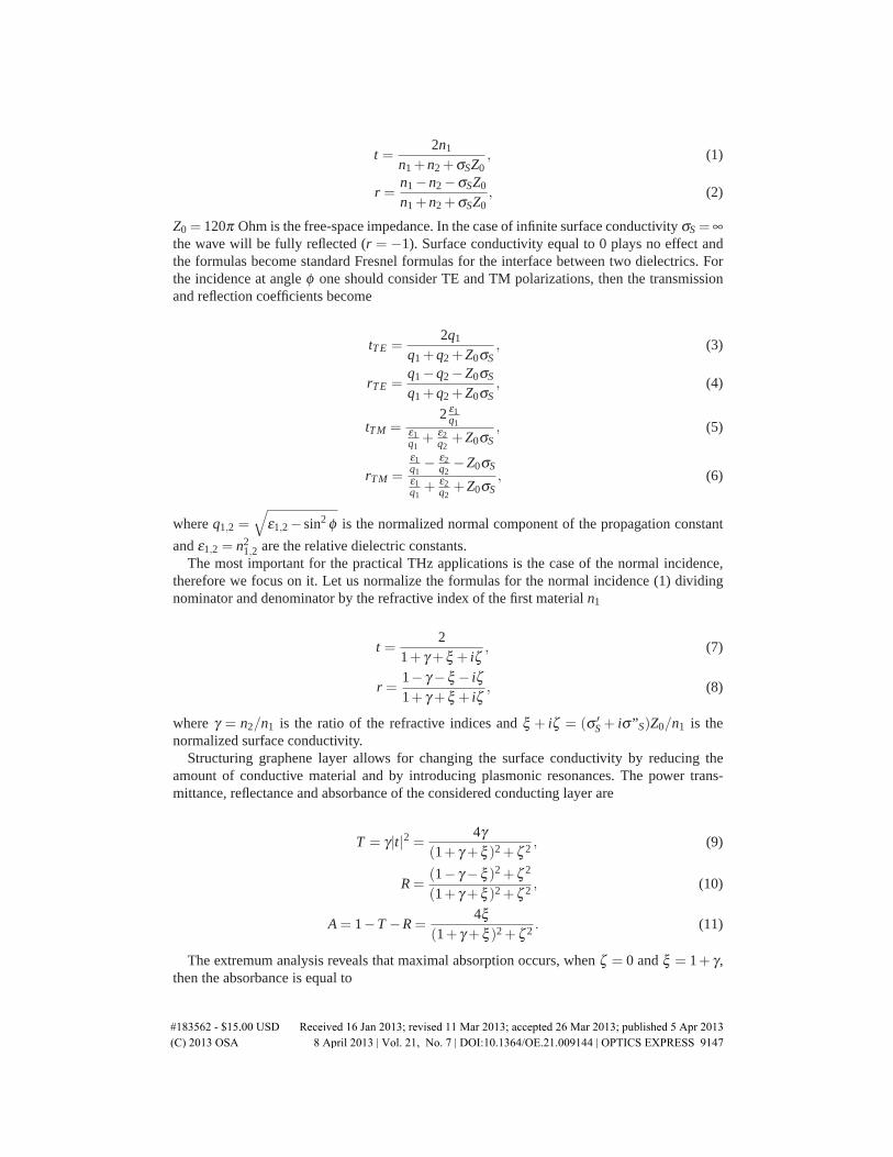
The effective surface conductivity approach is based on the transmission line analogy. It iswell-known, that propagation of a plane wave in a dielectric can be described by an equivalenttransmission line with perfect electric and perfect magnetic boundary conditions [28, 29]. Athin conducting layer with surface conductivity σS = σ ′
S + iσ”S at the flat boundary betweentwo dielectrics (refractive indices n1and n2, see Fig. 1) is equivalent to a load attached to thejunction between two transmission lines.
Fig. 1. The conductive interface (for example, graphene layer) between two dielectrics isequivalent to a load attached to the junction between two transmission lines.
If the thickness of the conductive layer is much smaller than the wavelength (that is truefor graphene in the ultrabroad range of spectrum from radiowaves to deep ultraviolet), thanwe can neglect the thickness and consider the conductive layer as a point load. For the normalincidence the amplitude transmission and reflection coefficients for a wave coming from thefirst dielectric are [18]
#183562 - $15.00 USD Received 16 Jan 2013; revised 11 Mar 2013; accepted 26 Mar 2013; published 5 Apr 2013(C) 2013 OSA 8 April 2013 | Vol. 21, No. 7 | DOI:10.1364/OE.21.009144 | OPTICS EXPRESS 9146
t =2n1
n1 +n2 +σSZ0, (1)
r =n1 −n2 −σSZ0
n1 +n2 +σSZ0, (2)
Z0 = 120π Ohm is the free-space impedance. In the case of infinite surface conductivity σS = ∞the wave will be fully reflected (r = −1). Surface conductivity equal to 0 plays no effect andthe formulas become standard Fresnel formulas for the interface between two dielectrics. Forthe incidence at angle φ one should consider TE and TM polarizations, then the transmissionand reflection coefficients become
tTE =2q1
q1 +q2 +Z0σS, (3)
rTE =q1 −q2 −Z0σS
q1 +q2 +Z0σS, (4)
tTM =2 ε1
q1ε1q1+ ε2
q2+Z0σS
, (5)
rTM =
ε1q1− ε2
q2−Z0σS
ε1q1+ ε2
q2+Z0σS
, (6)
where q1,2 =√
ε1,2 − sin2 φ is the normalized normal component of the propagation constant
and ε1,2 = n21,2 are the relative dielectric constants.
The most important for the practical THz applications is the case of the normal incidence,therefore we focus on it. Let us normalize the formulas for the normal incidence (1) dividingnominator and denominator by the refractive index of the first material n1
t =2
1+ γ +ξ + iζ, (7)
r =1− γ −ξ − iζ1+ γ +ξ + iζ
, (8)
where γ = n2/n1 is the ratio of the refractive indices and ξ + iζ = (σ ′S + iσ”S)Z0/n1 is the
normalized surface conductivity.Structuring graphene layer allows for changing the surface conductivity by reducing the
amount of conductive material and by introducing plasmonic resonances. The power trans-mittance, reflectance and absorbance of the considered conducting layer are
T = γ|t|2 = 4γ(1+ γ +ξ )2 +ζ 2 , (9)
R =(1− γ −ξ )2 +ζ 2
(1+ γ +ξ )2 +ζ 2 , (10)
A = 1−T −R =4ξ
(1+ γ +ξ )2 +ζ 2 . (11)
The extremum analysis reveals that maximal absorption occurs, when ζ = 0 and ξ = 1+ γ ,then the absorbance is equal to
#183562 - $15.00 USD Received 16 Jan 2013; revised 11 Mar 2013; accepted 26 Mar 2013; published 5 Apr 2013(C) 2013 OSA 8 April 2013 | Vol. 21, No. 7 | DOI:10.1364/OE.21.009144 | OPTICS EXPRESS 9147
Amax =1
1+ γ. (12)
For the symmetric environment (n1 = n2, so γ = 1) the maximal absorbance cannot ex-ceed 0.5. We can, however, obtain larger absorbance for γ < 1 that corresponds to the caseof incidence from a high-dielectric material with n1 > n2. For example, γ = 0.29 for a silicon(n = 3.416) - air interface and Amax = 0.77. We should, however, take into account that in real-ity incidence from silicon requires the wave to be previously coupled into silicon from air thatgives transmittance 0.70. Therefore, the total absorption of the initial wave is 0.54, that is notmuch better than for a symmetrical case γ = 1.
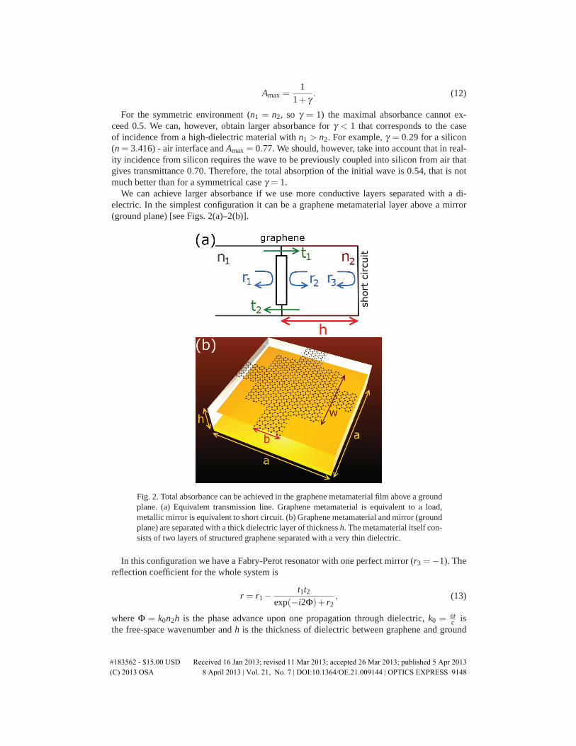
We can achieve larger absorbance if we use more conductive layers separated with a di-electric. In the simplest configuration it can be a graphene metamaterial layer above a mirror(ground plane) [see Figs. 2(a)–2(b)].
Fig. 2. Total absorbance can be achieved in the graphene metamaterial film above a groundplane. (a) Equivalent transmission line. Graphene metamaterial is equivalent to a load,metallic mirror is equivalent to short circuit. (b) Graphene metamaterial and mirror (groundplane) are separated with a thick dielectric layer of thickness h. The metamaterial itself con-sists of two layers of structured graphene separated with a very thin dielectric.
In this configuration we have a Fabry-Perot resonator with one perfect mirror (r3 =−1). Thereflection coefficient for the whole system is
r = r1 − t1t2exp(−i2Φ)+ r2
, (13)
where Φ = k0n2h is the phase advance upon one propagation through dielectric, k0 = ωc is
the free-space wavenumber and h is the thickness of dielectric between graphene and ground
#183562 - $15.00 USD Received 16 Jan 2013; revised 11 Mar 2013; accepted 26 Mar 2013; published 5 Apr 2013(C) 2013 OSA 8 April 2013 | Vol. 21, No. 7 | DOI:10.1364/OE.21.009144 | OPTICS EXPRESS 9148
plane. The meaning of the transmission and reflection coefficients t1, t2,r1,r2 is clear from theFig. 2(a) and their values are
t1 =2
1+ γ +ξ + iζ, (14)
t2 =2γ
1+ γ +ξ + iζ, (15)
r1 =1− γ −ξ − iζ1+ γ +ξ + iζ
, (16)
r2 =γ −1−ξ − iζ1+ γ +ξ + iζ
. (17)
After simple though tedious algebraic transformations we obtain absorbance
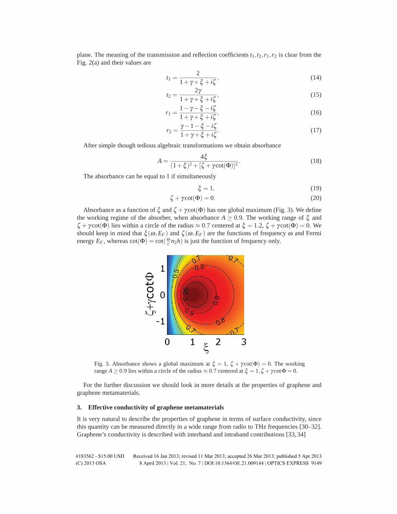
A =4ξ
(1+ξ )2 +[ζ + γ cot(Φ)]2. (18)
The absorbance can be equal to 1 if simultaneously
ξ = 1, (19)
ζ + γ cot(Φ) = 0. (20)
Absorbance as a function of ξ and ζ +γ cot(Φ) has one global maximum (Fig. 3). We definethe working regime of the absorber, when absorbance A ≥ 0.9. The working range of ξ andζ + γ cot(Φ) lies within a circle of the radius ≈ 0.7 centered at ξ = 1.2, ζ + γ cot(Φ) = 0. Weshould keep in mind that ξ (ω,EF) and ζ (ω,EF) are the functions of frequency ω and Fermienergy EF , whereas cot(Φ) = cot(ω
c n2h) is just the function of frequency only.
Fig. 3. Absorbance shows a global maximum at ξ = 1, ζ + γ cot(Φ) = 0. The workingrange A ≥ 0.9 lies within a circle of the radius ≈ 0.7 centered at ξ = 1,ζ + γ cotΦ = 0.
For the further discussion we should look in more details at the properties of graphene andgraphene metamaterials.
3. Effective conductivity of graphene metamaterials
It is very natural to describe the properties of graphene in terms of surface conductivity, sincethis quantity can be measured directly in a wide range from radio to THz frequencies [30–32].Graphene’s conductivity is described with interband and intraband contributions [33, 34]
#183562 - $15.00 USD Received 16 Jan 2013; revised 11 Mar 2013; accepted 26 Mar 2013; published 5 Apr 2013(C) 2013 OSA 8 April 2013 | Vol. 21, No. 7 | DOI:10.1364/OE.21.009144 | OPTICS EXPRESS 9149
σS = σ intraS +σ inter
S , (21)
σ intraS =
2kBTe2
π h2 ln(2coshEF
2kBT)
iω + iτ−1 , (22)
σ interS =
e2
4h[H(
ω2)+ i
4ωπ
∫ ∞
0
H(Ω)−H(ω2 )
ω2 −4Ω2 dΩ], (23)
where H(Ω) = sinh( hΩkBT )/[cosh( hΩ
kBT )+cosh( EFkBT )], T is the temperature, EF - electrochemical
potential (Fermi energy), ω- frequency of the electromagnetic wave and τ = 10−13 s - therelaxation time. For the THz frequencies, where the photon energy hω � EF , the interbandpart (23) is negligible comparing to the intraband. Therefore, in the THz range graphene is welldescribed by the Drude-like surface conductivity (22). For EF � kBT the conductivity dependslinearly on the Fermi energy
σS ≈ e2EF
π h2
iω + iτ−1 . (24)
For the numerical simulations graphene is usually represented as a layer of material of asmall thickness Δ with an in-plane effective permittivity
εe f f ,t = 1+ iσS
ε0ωΔ. (25)
The normal component of the effective permittivity εe f f ,n = 1.In other words we can say that graphene is represented by a thin metal with the plasma
frequency depending on the Fermi level
ωP = [2e2kBT
π h2ε0Δln(2cosh
EF
2kBT)]1/2. (26)
The conductivity of a continuous graphene film can be calculated analytically with expres-sion (22). However, for structured graphene metamaterials an analytical description is problem-atic and therefore we should turn to numerical methods. Tassin et al. [35] proposed to character-ize the thin-film metallic and graphene metamaterials with the electric and magnetic effective
surface conductivities σ (e)‖ and σ (m)
‖ and proposed the formulas for their retrieval for the sym-metric environment (the same homogeneous dielectric on the both sides from the metasurface).In this work we consider the normal incidence of the wave and a thin-film electric metamaterialin the asymmetric environment. In this situation the formula for the restoration of the effectivesurface conductivity σ e f f
S , which can be derived through the inversion of the Eq. (7), becomes
ξ + iζ =2t− (1+ γ). (27)
Some numerical programs (like, for example, CST Microwave Studio [36], which we used)calculate S21-parameter that is related to the amplitude transmission coefficient, as S21 =
√γt.The effective surface conductivity expressed through S21-parameter is
σ e f fS Z0 =
2S21
√n1n2 − (n1 +n2). (28)
We should mention that while the refractive index of the ambient dielectrics is of little im-portance for the restoration of continuous graphene surface conductivity (we do not consider
#183562 - $15.00 USD Received 16 Jan 2013; revised 11 Mar 2013; accepted 26 Mar 2013; published 5 Apr 2013(C) 2013 OSA 8 April 2013 | Vol. 21, No. 7 | DOI:10.1364/OE.21.009144 | OPTICS EXPRESS 9150
the influence of the substrate on the electronic structure and Fermi level), it becomes crucialfor the graphene metamaterial, since the frequency of the plasmonic resonance depends on thedielectric surrounding. Therefore, n1 and n2 should correspond to dielectrics that are involvedin the device fabrication.
Let us now look on values of the surface conductivities of graphene and graphene basedmetamaterials (Fig. 4). We should, however, make a comment on choosing the design of meta-materials. First of all, in order to tune their properties by electrostatic gating, there should beat least two layers of graphene separated with a thin dielectric spacer. Each of the graphenesheets then plays the role of a gate electrode. Applying the voltage moves the Fermi level inboth graphene layers [18], but in opposite directions. Nevertheless, if initially the Fermi level isat the Dirac point, the changes of graphene conductivity in both layers are the same. Employingthe ground plane [Fig. 2(b)] as a gate electrode does not suit, since as we will see further thedielectric separation between graphene metamaterial and ground plane should be on the orderof several tens of micrometers, that requires high gating voltages of tens of kV for noticeablechange in conductivity.
Second, structured graphene layer should be electrically connected, otherwise we cannotchange the properties of the whole layer by applying voltage. Therefore metamaterials, consist-ing of isolated graphene patches are not suitable for tunable devices.
Third, in order to make the metamaterial polarization insensitive (under normal incidence),its unit cell should be at least C4 symmetric.
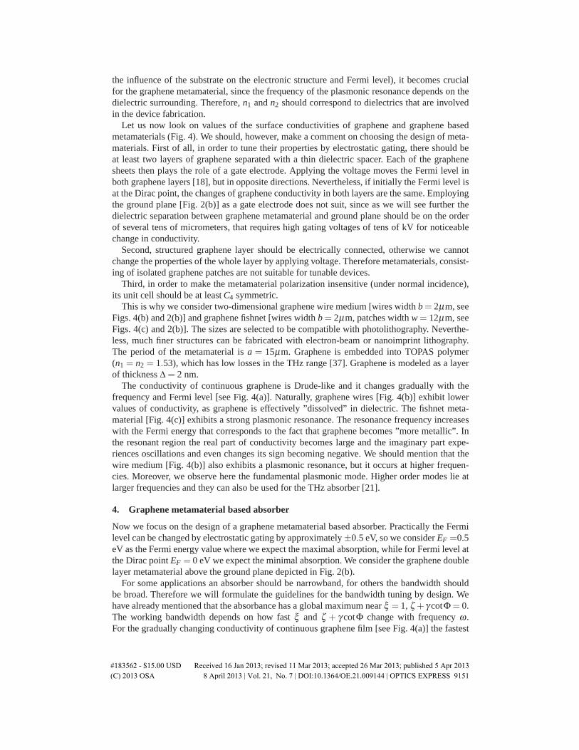
This is why we consider two-dimensional graphene wire medium [wires width b = 2μm, seeFigs. 4(b) and 2(b)] and graphene fishnet [wires width b = 2μm, patches width w = 12μm, seeFigs. 4(c) and 2(b)]. The sizes are selected to be compatible with photolithography. Neverthe-less, much finer structures can be fabricated with electron-beam or nanoimprint lithography.The period of the metamaterial is a = 15μm. Graphene is embedded into TOPAS polymer(n1 = n2 = 1.53), which has low losses in the THz range [37]. Graphene is modeled as a layerof thickness Δ = 2 nm.
The conductivity of continuous graphene is Drude-like and it changes gradually with thefrequency and Fermi level [see Fig. 4(a)]. Naturally, graphene wires [Fig. 4(b)] exhibit lowervalues of conductivity, as graphene is effectively ”dissolved” in dielectric. The fishnet meta-material [Fig. 4(c)] exhibits a strong plasmonic resonance. The resonance frequency increaseswith the Fermi energy that corresponds to the fact that graphene becomes ”more metallic”. Inthe resonant region the real part of conductivity becomes large and the imaginary part expe-riences oscillations and even changes its sign becoming negative. We should mention that thewire medium [Fig. 4(b)] also exhibits a plasmonic resonance, but it occurs at higher frequen-cies. Moreover, we observe here the fundamental plasmonic mode. Higher order modes lie atlarger frequencies and they can also be used for the THz absorber [21].
4. Graphene metamaterial based absorber
Now we focus on the design of a graphene metamaterial based absorber. Practically the Fermilevel can be changed by electrostatic gating by approximately ±0.5 eV, so we consider EF =0.5eV as the Fermi energy value where we expect the maximal absorption, while for Fermi level atthe Dirac point EF = 0 eV we expect the minimal absorption. We consider the graphene doublelayer metamaterial above the ground plane depicted in Fig. 2(b).
For some applications an absorber should be narrowband, for others the bandwidth shouldbe broad. Therefore we will formulate the guidelines for the bandwidth tuning by design. Wehave already mentioned that the absorbance has a global maximum near ξ = 1, ζ +γ cotΦ = 0.The working bandwidth depends on how fast ξ and ζ + γ cotΦ change with frequency ω .For the gradually changing conductivity of continuous graphene film [see Fig. 4(a)] the fastest
#183562 - $15.00 USD Received 16 Jan 2013; revised 11 Mar 2013; accepted 26 Mar 2013; published 5 Apr 2013(C) 2013 OSA 8 April 2013 | Vol. 21, No. 7 | DOI:10.1364/OE.21.009144 | OPTICS EXPRESS 9151
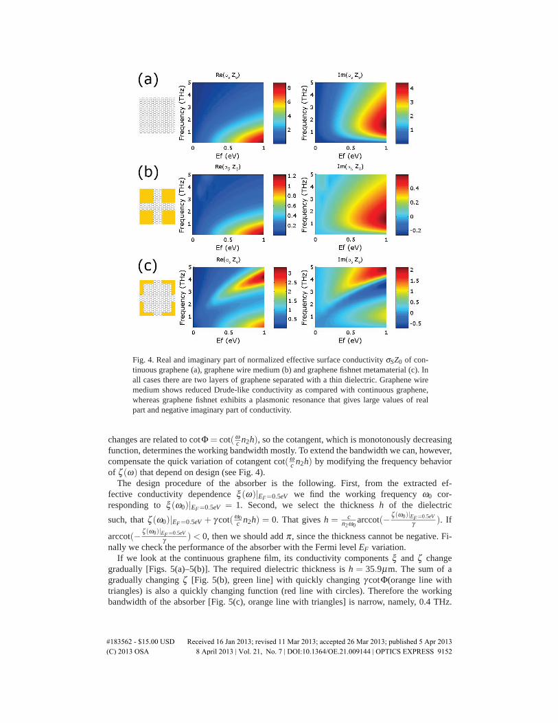
Fig. 4. Real and imaginary part of normalized effective surface conductivity σSZ0 of con-tinuous graphene (a), graphene wire medium (b) and graphene fishnet metamaterial (c). Inall cases there are two layers of graphene separated with a thin dielectric. Graphene wiremedium shows reduced Drude-like conductivity as compared with continuous graphene,whereas graphene fishnet exhibits a plasmonic resonance that gives large values of realpart and negative imaginary part of conductivity.
changes are related to cotΦ = cot(ωc n2h), so the cotangent, which is monotonously decreasing
function, determines the working bandwidth mostly. To extend the bandwidth we can, however,compensate the quick variation of cotangent cot(ω
c n2h) by modifying the frequency behaviorof ζ (ω) that depend on design (see Fig. 4).
The design procedure of the absorber is the following. First, from the extracted ef-fective conductivity dependence ξ (ω)|EF=0.5eV we find the working frequency ω0 cor-responding to ξ (ω0)|EF=0.5eV = 1. Second, we select the thickness h of the dielectric
such, that ζ (ω0)|EF=0.5eV + γ cot(ω0c n2h) = 0. That gives h = c
n2ω0arccot(− ζ (ω0)|EF=0.5eV
γ ). If
arccot(− ζ (ω0)|EF=0.5eV
γ ) < 0, then we should add π , since the thickness cannot be negative. Fi-nally we check the performance of the absorber with the Fermi level EF variation.
If we look at the continuous graphene film, its conductivity components ξ and ζ changegradually [Figs. 5(a)–5(b)]. The required dielectric thickness is h = 35.9μm. The sum of agradually changing ζ [Fig. 5(b), green line] with quickly changing γ cotΦ(orange line withtriangles) is also a quickly changing function (red line with circles). Therefore the workingbandwidth of the absorber [Fig. 5(c), orange line with triangles] is narrow, namely, 0.4 THz.
#183562 - $15.00 USD Received 16 Jan 2013; revised 11 Mar 2013; accepted 26 Mar 2013; published 5 Apr 2013(C) 2013 OSA 8 April 2013 | Vol. 21, No. 7 | DOI:10.1364/OE.21.009144 | OPTICS EXPRESS 9152
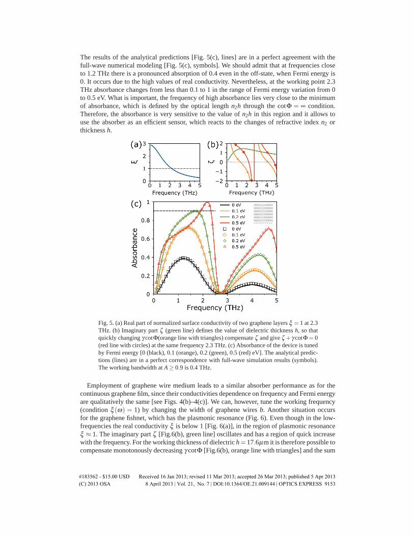
The results of the analytical predictions [Fig. 5(c), lines] are in a perfect agreement with thefull-wave numerical modeling [Fig. 5(c), symbols]. We should admit that at frequencies closeto 1.2 THz there is a pronounced absorption of 0.4 even in the off-state, when Fermi energy is0. It occurs due to the high values of real conductivity. Nevertheless, at the working point 2.3THz absorbance changes from less than 0.1 to 1 in the range of Fermi energy variation from 0to 0.5 eV. What is important, the frequency of high absorbance lies very close to the minimumof absorbance, which is defined by the optical length n2h through the cotΦ = ∞ condition.Therefore, the absorbance is very sensitive to the value of n2h in this region and it allows touse the absorber as an efficient sensor, which reacts to the changes of refractive index n2 orthickness h.
Fig. 5. (a) Real part of normalized surface conductivity of two graphene layers ξ = 1 at 2.3THz. (b) Imaginary part ζ (green line) defines the value of dielectric thickness h, so thatquickly changing γ cotΦ(orange line with triangles) compensate ζ and give ζ +γ cotΦ = 0(red line with circles) at the same frequency 2.3 THz. (c) Absorbance of the device is tunedby Fermi energy [0 (black), 0.1 (orange), 0.2 (green), 0.5 (red) eV]. The analytical predic-tions (lines) are in a perfect correspondence with full-wave simulation results (symbols).The working bandwidth at A ≥ 0.9 is 0.4 THz.
Employment of graphene wire medium leads to a similar absorber performance as for thecontinuous graphene film, since their conductivities dependence on frequency and Fermi energyare qualitatively the same [see Figs. 4(b)–4(c)]. We can, however, tune the working frequency(condition ξ (ω) = 1) by changing the width of graphene wires b. Another situation occursfor the graphene fishnet, which has the plasmonic resonance (Fig. 6). Even though in the low-frequencies the real conductivity ξ is below 1 [Fig. 6(a)], in the region of plasmonic resonanceξ ≈ 1. The imaginary part ζ [Fig.6(b), green line] oscillates and has a region of quick increasewith the frequency. For the working thickness of dielectric h= 17.6μm it is therefore possible tocompensate monotonously decreasing γ cotΦ [Fig.6(b), orange line with triangles] and the sum
#183562 - $15.00 USD Received 16 Jan 2013; revised 11 Mar 2013; accepted 26 Mar 2013; published 5 Apr 2013(C) 2013 OSA 8 April 2013 | Vol. 21, No. 7 | DOI:10.1364/OE.21.009144 | OPTICS EXPRESS 9153
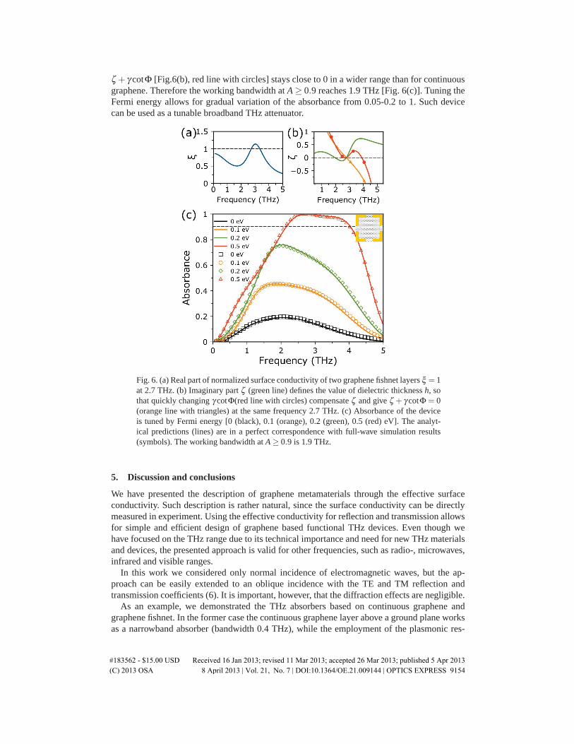
ζ + γ cotΦ [Fig.6(b), red line with circles] stays close to 0 in a wider range than for continuousgraphene. Therefore the working bandwidth at A ≥ 0.9 reaches 1.9 THz [Fig. 6(c)]. Tuning theFermi energy allows for gradual variation of the absorbance from 0.05-0.2 to 1. Such devicecan be used as a tunable broadband THz attenuator.
Fig. 6. (a) Real part of normalized surface conductivity of two graphene fishnet layers ξ = 1at 2.7 THz. (b) Imaginary part ζ (green line) defines the value of dielectric thickness h, sothat quickly changing γ cotΦ(red line with circles) compensate ζ and give ζ + γ cotΦ = 0(orange line with triangles) at the same frequency 2.7 THz. (c) Absorbance of the deviceis tuned by Fermi energy [0 (black), 0.1 (orange), 0.2 (green), 0.5 (red) eV]. The analyt-ical predictions (lines) are in a perfect correspondence with full-wave simulation results(symbols). The working bandwidth at A ≥ 0.9 is 1.9 THz.
5. Discussion and conclusions
We have presented the description of graphene metamaterials through the effective surfaceconductivity. Such description is rather natural, since the surface conductivity can be directlymeasured in experiment. Using the effective conductivity for reflection and transmission allowsfor simple and efficient design of graphene based functional THz devices. Even though wehave focused on the THz range due to its technical importance and need for new THz materialsand devices, the presented approach is valid for other frequencies, such as radio-, microwaves,infrared and visible ranges.
In this work we considered only normal incidence of electromagnetic waves, but the ap-proach can be easily extended to an oblique incidence with the TE and TM reflection andtransmission coefficients (6). It is important, however, that the diffraction effects are negligible.
As an example, we demonstrated the THz absorbers based on continuous graphene andgraphene fishnet. In the former case the continuous graphene layer above a ground plane worksas a narrowband absorber (bandwidth 0.4 THz), while the employment of the plasmonic res-
#183562 - $15.00 USD Received 16 Jan 2013; revised 11 Mar 2013; accepted 26 Mar 2013; published 5 Apr 2013(C) 2013 OSA 8 April 2013 | Vol. 21, No. 7 | DOI:10.1364/OE.21.009144 | OPTICS EXPRESS 9154
onance in a structured graphene metamaterial allows for a broadband tunable absorber (band-width 1.9 THz).
A wide range of other terahertz devices can be described with the effective surface conduc-tivity approach: modulators, tunable filters, polarizers, polarization converters, sensors, etc. Webelieve, that this approach will become a useful tool for the emerging field of graphene terahertzphotonics.
Acknowledgments
The authors thank D. Chigrin, J.C. Due Buron, F. Pizzocchero and S. Zhukovsky for usefuldiscussions. A.A. acknowledges the financial support from the Danish Council for Technicaland Production Sciences through the GraTer (11-116991) project.
#183562 - $15.00 USD Received 16 Jan 2013; revised 11 Mar 2013; accepted 26 Mar 2013; published 5 Apr 2013(C) 2013 OSA 8 April 2013 | Vol. 21, No. 7 | DOI:10.1364/OE.21.009144 | OPTICS EXPRESS 9155