gravure-printed electronics: devices, technology development …€¦ · ·...
TRANSCRIPT

Gravure-printed electronics: Devices, technologydevelopment and design
Gerd Grau
Electrical Engineering and Computer SciencesUniversity of California at Berkeley
Technical Report No. UCB/EECS-2017-17http://www2.eecs.berkeley.edu/Pubs/TechRpts/2017/EECS-2017-17.html
May 1, 2017

Copyright © 2017, by the author(s).All rights reserved.
Permission to make digital or hard copies of all or part of this work forpersonal or classroom use is granted without fee provided that copies arenot made or distributed for profit or commercial advantage and that copiesbear this notice and the full citation on the first page. To copy otherwise, torepublish, to post on servers or to redistribute to lists, requires priorspecific permission.
Gravure-printed electronics: Devices, technology development and design
By
Gerd Fritz Milan Nino Grau
A dissertation submitted in partial satisfaction of the
requirements for the degree of
Doctor of Philosophy
in
Engineering – Electrical Engineering and Computer Sciences
in the
Graduate Division
of the
University of California, Berkeley
Committee in charge:
Professor Vivek Subramanian, Chair
Professor Andrew R. Neureuther
Professor Costas P. Grigoropoulos
Spring 2016

Copyright © 2016, by the author(s).
All rights reserved.
Permission to make digital or hard copies of all or part of this work for personal or classroom use
is granted without fee provided that copies are not made or distributed for profit or commercial
advantage and that copies bear this notice and the full citation on the first page. To copy otherwise,
to republish, to post on servers or to redistribute to lists, requires prior specific permission.
1
Abstract
Gravure-printed electronics: Devices, technology development and design
by
Gerd Fritz Milan Nino Grau
Doctor of Philosophy in Engineering – Electrical Engineering and Computer Sciences
University of California, Berkeley
Professor Vivek Subramanian, Chair
Printed electronics is a novel microfabrication paradigm that is particularly well suited for
fabrication of low-cost, large-area electronics on flexible substrates. Applications include flexible
displays, solar cells, RFID tags or sensor networks. Gravure printing is a particularly promising
printing technique because it combines high print speed with high resolution patterning. In this
thesis, gravure printing for printed electronics is advanced on multiple levels. The gravure process
is advanced in terms of tooling and understanding of printing physics as well as its application to
substrate preparation and device fabrication.
Gravure printing is applied to transform paper into a viable substrate for printed electronics. Paper
is very attractive for printed electronics because it is low-cost, biodegradable, lightweight and
ubiquitous. However, printing of high-performance electronic devices onto paper has been limited
by the large surface roughness and ink absorption of paper. This is overcome here by gravure
printing a local smoothing layer and printed organic thin-film transistors (OTFTs) are
demonstrated to exhibit performance on-par with device on plastic substrates.
If highly-scaled features are to be printed by gravure, traditional gravure roll making techniques
are limited in terms of pattern definition and surface finish. Here, a novel fabrication process for
gravure rolls is demonstrated utilizing silicon microfabrication. Sub-3µm features are printed at
1m/s. Proximity effects are demonstrated for more complex highly-scaled features. The fluid
mechanics of this effect is studied and it is suggested how it can be used to enhance feature quality
by employing assist features.
Finally, advancements are made to printed organic thin-film transistors as an important technology
driver and demonstrator for printed electronics. First, a novel scanned thermal annealing technique
is presented that significantly improves the crystallization of an organic semiconductor and
electrical performance. Second, transistors are fully gravure printed at a high print speed of 1m/s.
By scaling both lateral and thickness dimensions and optimizing the printing processes, good
electrical performance, low-voltage operation and low variability is demonstrated.
i
Acknowledgements
I would like to thank a number of people who made this work possible as well as enjoyable. First
and foremost I would like to thank my advisor Professor Vivek Subramanian. Throughout my time
in graduate school he always pushed me to achieve more and gave me guidance when needed
whilst giving me the freedom to pursue what interested me and become an independent researcher.
I learned many important lessons from him that will be invaluable in the future – be it in research,
mentoring, writing or teaching. I want to thank my dissertation committee members Professor
Andy Neureuther and Professor Costas Grigoropoulos and Professor Ana Claudia Arias who was
the chair of my qualifying exam committee. I am also very grateful to Professor Hayden Taylor
and Professor Randy Schunk who were great collaborators and mentors during my job search. I
am indebted to Professor Clark Nguyen who gave me the chance to teach a class over one summer,
which was a very important experience on my road to an academic career.
None of this work would have been possible without collaborators both within the Printed
Electronics group at Berkeley as well as from other groups. I am especially thankful to those who
worked on gravure printing at the same time as me and with whom I shared many insightful
discussions, namely Rungrot (Jack) Kitsomboonloha, Hongki Kang, William Scheideler, Artos
Cen and Daniel Hariprasad. Sharing a lab with a large number of people over the years working
on a variety of projects has given me many interesting perspectives and practical help with my
projects as well as many enjoyable moments. For that I am grateful to Steve Volkman, Lakshmi
Jagannathan, Michael Tseng, Jaewon Jang, Eungseok Park, Feng Pan, Kyle Braam, Sarah Swisher,
Jake Sadie, Rumi Karim, Andre Zeumault, Adrien Pierre, Garret McKerricher, Seungjun Chung,
Jeremy Smith, Nishita Deka, Carlos Biaou and Matt McPhail.
Both the Nanolab and the Cory machine shop staff were always very helpful when I needed to
solve a tool problem or build a custom setup. The mailroom in Sutardja Dai was another place
with very friendly people who helped me out many times. I also want to thank Charlotte Jones and
Gwen Lindsey who were always very helpful when I needed administrative assistance.
Over the years I have received funding from a number of sources that I am grateful for. I would
like to highlight the NASCENT NSF ERC whose semiannual meetings in Austin and Albuquerque
were always a great way to meet researchers from other universities as well as Merck who not only
provided funding but also organic materials that I used for most of my transistor work.
My family – my parents, my sister and her husband – was always there for me during these years
giving me support, advice and perspective in many different situations. Lastly, but most
importantly, I want to thank my fiancée Angela. She was patient with me when I worked long
hours in the lab, when I wanted to endlessly discuss research or career directions (and she gave me
good feedback) or when I told a new acquaintance about my research for the 1000th time in her
presence. Spending my free time with her has made every moment of my life enjoyable. Meeting
her has been the best result of my time at Berkeley.

ii
Table of Contents
Chapter 1: Introduction ............................................................................................................... 1
1.1 Printed Electronics ........................................................................................................... 1
1.2 Comparison of different printing techniques ................................................................... 3
1.3 Fluid mechanics at the microscale ................................................................................... 5
1.3.1 Viscous forces ........................................................................................................... 6
1.3.2 Surface tension forces ............................................................................................... 7
1.4 Overview of gravure printing process ............................................................................ 12
1.4.1 Cell filling ............................................................................................................... 13
1.4.2 Doctor blade wiping ................................................................................................ 15
1.4.3 Ink transfer .............................................................................................................. 18
1.4.4 Pattern formation on the substrate .......................................................................... 20
1.4.5 Overall process optimization .................................................................................. 21
1.5 Printed organic thin-film transistors (OTFTs) ............................................................... 22
1.6 Thesis organization ........................................................................................................ 24
Chapter 2: Gravure printing enabled transistors on novel paper substrates ............................. 26
2.1 Introduction .................................................................................................................... 26
2.2 Paper characterization .................................................................................................... 27
2.3 Paper modification ......................................................................................................... 31
2.4 Printed devices on smoothed paper ................................................................................ 39
2.4.1 Dielectric evaluation ............................................................................................... 39
2.4.2 Printed transistors on paper ..................................................................................... 42
2.4.3 Bending tests ........................................................................................................... 47
2.5 Conclusions .................................................................................................................... 48
Chapter 3: Fabrication of gravure roll for high-resolution printing ......................................... 50
3.1 Introduction .................................................................................................................... 50
3.2 Roll fabrication process .................................................................................................. 53
3.3 Printing results................................................................................................................ 57
3.3.1 Plate mounting on magnetic roller .......................................................................... 57
3.3.2 Printing optimization .............................................................................................. 59
iii
3.3.3 Effect of hard layer on roll scratching .................................................................... 63
3.4 Conclusions .................................................................................................................... 65
Chapter 4: Proximity effects in high-resolution gravure printing ............................................ 66
4.1 Introduction .................................................................................................................... 66
4.2 Experimental .................................................................................................................. 68
4.3 Printed pattern analysis .................................................................................................. 69
4.3.1 Proximity effect ...................................................................................................... 69
4.3.2 Automated pattern analysis ..................................................................................... 71
4.3.3 Design rules and assist features .............................................................................. 73
4.4 Proximity effect fluid mechanics ................................................................................... 78
4.4.1 Fluid analysis on printing plate ............................................................................... 78
4.4.2 Ink transfer .............................................................................................................. 80
4.4.3 Proximity effect analysis......................................................................................... 83
4.5 Conclusions .................................................................................................................... 99
Chapter 5: Printed organic thin-film transistors ..................................................................... 100
5.1 Introduction .................................................................................................................. 100
5.2 A novel scanned thermal annealing technique to optimize organic semiconductor
crystallization .......................................................................................................................... 101
5.2.1 Simulation of thermal gradient ............................................................................. 103
5.2.2 Device fabrication ................................................................................................. 106
5.2.3 Results and discussion .......................................................................................... 107
5.3 Fully gravure printed organic thin-film transistors ...................................................... 113
5.3.1 Device fabrication ................................................................................................. 114
5.3.2 Device characterization ......................................................................................... 127
5.4 Conclusions .................................................................................................................. 135
Chapter 6: Conclusions and future work ................................................................................ 136
6.1 Conclusions .................................................................................................................. 136
6.2 Future work .................................................................................................................. 137
Chapter 7: References ............................................................................................................. 140
Appendix A: Bending test strain calculation .............................................................................. 150
1
Chapter 1: Introduction
1.1 Printed Electronics
The graphics arts industry has used printing techniques for centuries to print patterns of colored
ink onto innumerable products. This has led to the development of very sophisticated printing
machines, processes and inks. Patterns can be printed onto very large webs that are several meters
wide at high print speeds on the order of 10m/s. This results in very large production throughput
and thus low-cost production per unit area of the substrate. The vision of printed electronics is to
leverage this expertise to fabricate low-cost, large-area electronics.1–3 Applications that are
fundamentally large-area are particularly promising to take advantage of the low cost per unit area
offered by printing. Such applications include displays, solar cells, RFID antennas or sensor
networks (see Figure 1-1). Another factor that significantly increases the throughput of printing
techniques is their additive nature. Ink is only deposited where it is actually needed. This is very
different from traditional microfabrication techniques that are subtractive. Traditionally, blanket
layers are deposited by techniques such as chemical vapor deposition (CVD), evaporation,
sputtering or thermal oxidation. In order to create functional patterns such as lines or squares, these
blanket layers need to be patterned. Typically, photolithography is employed to pattern photoresist
that protects the desired pattern whilst unwanted material is etched away. This process involves
several steps and tools, some of which require slow vacuum processing, which further degrades
process throughput. In contrast, printing is a one-step, additive process, which not only improves
throughput but also material utilization.
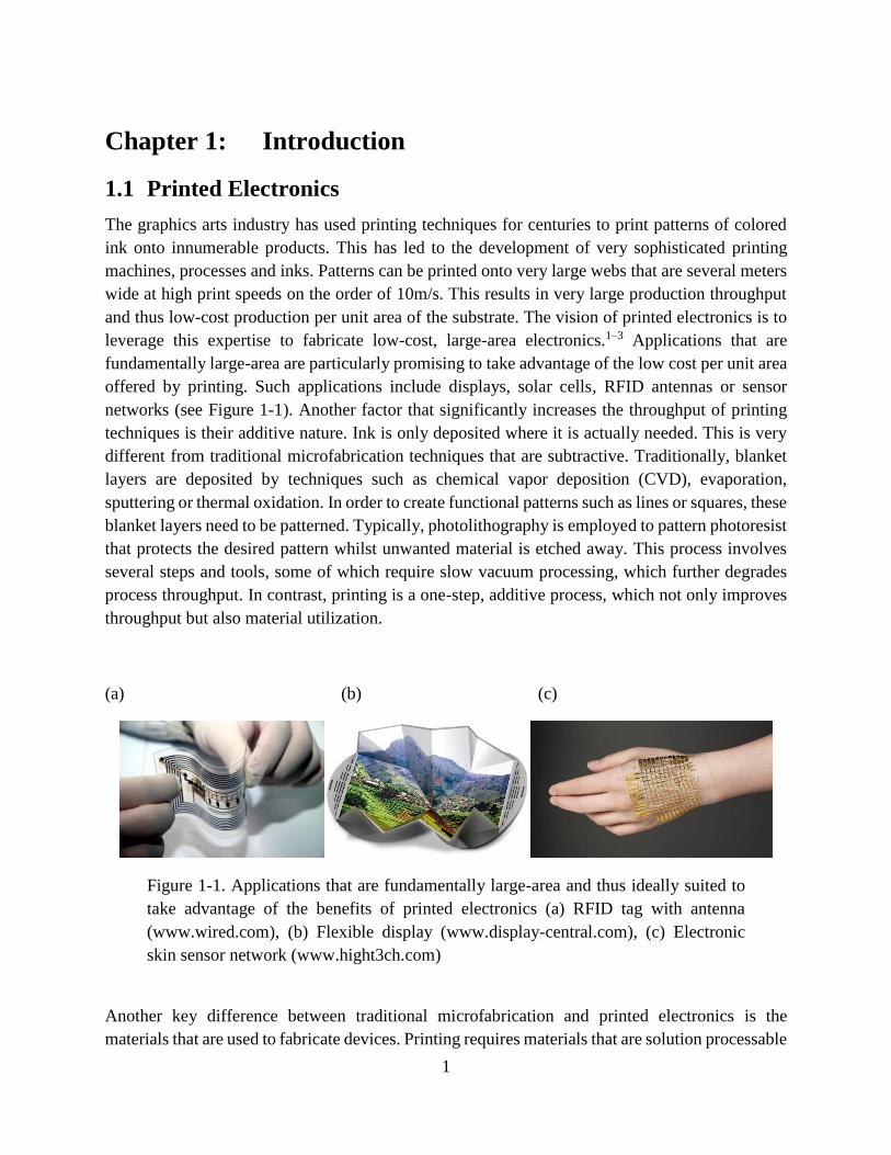
(a) (b) (c)
Figure 1-1. Applications that are fundamentally large-area and thus ideally suited to
take advantage of the benefits of printed electronics (a) RFID tag with antenna
(www.wired.com), (b) Flexible display (www.display-central.com), (c) Electronic
skin sensor network (www.hight3ch.com)
Another key difference between traditional microfabrication and printed electronics is the
materials that are used to fabricate devices. Printing requires materials that are solution processable
2
since printing deposits liquid inks. This means the active material is dissolved or dispersed in a
solvent during printing. The solvent is evaporated after printing and the material is converted into
its final state. The temperature at which this conversion process occurs constrains the choice of
substrate material. If flexible substrates such as low-cost plastic are used, processing temperatures
cannot exceed about 200°C and for some plastics need to be even lower.4 Both of these
requirements, solution processability and low thermal budget, make organic materials attractive
for printed electronics.5–7 In particular, dielectrics and semiconductors can be fabricated from
polymer and small molecule materials. Such materials can be readily dissolved in a variety of
organic solvents and typical processing temperatures are around 100°C. However, conductors
fabricated from organic materials tend to exhibit poor conductivity compared with metals.8 Thus,
metal nanoparticles are widely used to print the electrodes for organic devices.9–11 Organic ligands
are attached to metal nanoparticles to solubilize them in solvents and formulate inks. Due to the
small size of these nanoparticles (diameter on the order of 10nm), they exhibit a very large surface
to volume ratio, which results in a significantly reduced melting temperature. Thus, metal
nanoparticles can be sintered at plastic compatible temperatures to form conductive patterns. The
combination of metal nanoparticle and organic inks enables the printing of conductors,
semiconductors and dielectrics on low-cost plastic substrates to print complete microelectronic
devices.
A range of different devices has been fabricated using printing techniques. This includes
transistors12–26,24,27,28, sensors29,30, MEMS devices31,32, batteries33, solar cells34, organic light-
emitting diodes (OLEDs)35, antennas36 and passive components37. By putting these devices
together, fully printed systems can be fabricated. The performance of printed electronics still
remains limited by low resolution and low performance materials compared with traditional silicon
CMOS processes. It is thus paramount to choose applications that do not require very high
performance whilst benefitting from the unique advantages that printed electronics offers. Printing
is ideal for large-area, low-cost applications on flexible substrates. Such applications include RFID
tags38, flexible displays39 and large-area sensing40. Whilst these applications do not require
performance on par with traditional silicon microelectronics, the performance of printing processes
and printed devices does need to be pushed further to enable real systems. In this dissertation, the
performance of gravure printing as well as the performance of printed transistors is pushed towards
fully printed systems.
The choice of gravure printing as the focus of this dissertation is discussed in the next section by
contrasting different printing techniques that offer different benefits and drawbacks. The physics
of gravure printing that underpins large parts of this thesis are described next after a more general
section describing fluid mechanics at the microscale. This fluid mechanical understanding is
crucial in order to understand the flow of liquid inks during the printing process. The state-of-the-
3
art in printed transistors, which are the main technology demonstration in this thesis, is discussed
in the following section. Finally, an overview of the thesis organization is given.
1.2 Comparison of different printing techniques
Many different printing techniques have been proposed for printed electronics.41,42,3 Each printing
technique has its own particular advantages and disadvantages and thus complex systems will
likely be fabricated by a combination of different techniques. There are many different
categorizations by which printing methods can be classified. The two most immediate dimensions
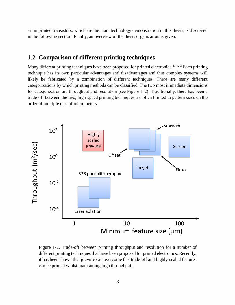
for categorization are throughput and resolution (see Figure 1-2). Traditionally, there has been a
trade-off between the two; high-speed printing techniques are often limited to pattern sizes on the
order of multiple tens of micrometers.
Figure 1-2. Trade-off between printing throughput and resolution for a number of
different printing techniques that have been proposed for printed electronics. Recently,
it has been shown that gravure can overcome this trade-off and highly-scaled features
can be printed whilst maintaining high throughput.
4
One broad category of printing methods is digital methods such as inkjet printing. Such techniques
offer the advantage of being able to easily change patterns on the fly. This is a great advantage in
research and prototyping. However, throughput, reliability and resolution are challenges. Inkjet
deposits material by jetting droplets from a nozzle that is scanned relative to the substrate. In order
to achieve high throughput, a large number of nozzles must be used, which increases the risk of
nozzle clogging. Similarly, downscaling of feature size is limited by the nozzle size and drop
placement accuracy, especially at high print speeds.16,43 When downscaling nozzle size, the risk of
clogging increases and droplet deviation also worsens. Thus, non-digital printing methods such as
screen printing, offset, flexography and gravure are more promising for scaled-up high-throughput
manufacturing. These contact printing techniques offer superior pattern fidelity because no jetting
from a nozzle is involved. Screen printing is unique in this list because ink is pushed through a
mesh onto the substrate. The mesh acts as a support for the stencil that defines the pattern. Screen
printing requires high viscosity inks, which makes it ideally suited for the deposition of thick
films.41 The printing of high-resolution features is limited by the mesh. Small feature sizes require
a larger mesh count per unit area i.e. smaller openings in the mesh to support the fine features on
the mask. This limits the amount of high viscosity ink that can be pushed through the mesh leading
to non-uniform features.44 Thus, the resolution of screen printing is limited to several micrometers;
indeed, in commercial use, screen printing typically delivers resolutions worse than tens of
micrometers.45,46 Conversely, offset, flexography and gravure printing all use a roll that is inked,
from which patterned ink is transferred to the substrate. They differ in how the pattern is created
on the roll. In flexography the pattern consists of raised features that are inked from an anilox
roller. The resolution of flexography is limited by the low stiffness of the material from which the
patterned roll is fabricated leading to the over compression of fine features during the printing
process and reduced pattern fidelity.47 Offset and gravure are most promising in terms of resolution
and print speed. In offset, the pattern and non-pattern areas lie in the same plane on the roll.
Patterning is achieved by differences in surface energy. The main drawback is the difficulty in
creating inks where the right combination of surface energies, ink surface tension and ink viscosity
gives good patterning. In gravure printing, the pattern is made up of recessed cells below the roll
surface. These cells are filled with ink and excess ink is removed from the land areas in between
the cells using a doctor blade (see Figure 1-3 for an overview of the gravure process). The pattern
is typically pixelated into individual square cells. An analogous technique, intaglio printing, makes
use of continuous trenches; this is avoided in gravure since the use of such trenches causes the
print quality to be much more orientation dependent.48 Gravure cylinders are typically made from
metals such as copper with a chromium coating. This results in excellent dimensional stability,
durability and pattern fidelity as well as compatibility with a wide range of solvents. The main
challenge with gravure is non-idealities during the doctor blade wiping process. Recently, it has
been demonstrated that by understanding the underlying physics in detail, gravure printing can be
pushed into a highly-scaled regime with feature sizes well below 10µm whilst still printing at high
speeds on the order of 1m/s.23,49 This makes gravure a very promising technique to deliver high-
performance, low-cost printed electronics and it will be the focus of this dissertation.

5
In order to push the performance of gravure printing, one needs to understand the underlying
physical principles of the printing process. Before describing the specifics of the gravure process,
it is instructive to consider fluid mechanics at the microscale more generally. The next section
describes the forces and phenomena that dictate the behavior of the liquid ink in the gravure
process as well as in many other printing processes.
Figure 1-3. Overview of the gravure process and its four sub-processes: cell filling,
doctor blade wiping, ink transfer and ink spreading on the substrate. Courtesy of
Rungrot Kitsomboonloha.
1.3 Fluid mechanics at the microscale
Printing means the deposition of liquid inks. Thus, it is imperative to understand the fluid
mechanical processes that occur during the printing process. In this section, the basic fluid
mechanics that underpins many aspects of this thesis will be discussed. This discussion will focus
on effects that occur at the microscale to enable highly-scaled printing of microelectronics. At the
microscale, the two most important forces experienced by fluids are surface tension and viscous
forces. Other forces such as gravity and inertial forces scale with the geometrical dimensions of
the system. This can be seen from dimensionless numbers that represent the relative magnitudes
of these forces:

6
Reynolds number: 𝑅𝑒 =𝑖𝑛𝑒𝑟𝑡𝑖𝑎𝑙
𝑣𝑖𝑠𝑐𝑜𝑢𝑠=
𝜌𝑈𝐿
𝜇 Eq. 1-1
Bond number: 𝐵𝑜 =𝑔𝑟𝑎𝑣𝑖𝑡𝑦
𝑠𝑢𝑟𝑓𝑎𝑐𝑒 𝑡𝑒𝑛𝑠𝑖𝑜𝑛=
∆𝜌𝑔𝐿2
𝜎 Eq. 1-2
Capillary number: 𝐶𝑎 =𝑣𝑖𝑠𝑐𝑜𝑢𝑠
𝑠𝑢𝑟𝑓𝑎𝑐𝑒 𝑡𝑒𝑛𝑠𝑖𝑜𝑛=
𝜇𝑈
𝜎 Eq. 1-3
Where ρ is the fluid density, U is a characteristic velocity of the problem (for example print speed),
L is a characteristic length scale of the problem (for example channel width), µ is the fluid
viscosity, Δρ is the density difference between two fluids that leads to gravitational forces, g is the
gravitational acceleration and σ is the fluid surface tension. As the characteristic length scale L is
scaled down to the microscale, inertial and gravity forces diminish relative to viscous and surface
tension forces. There are some situations in printing where inertia does play an important role such
as when ejecting low-viscosity droplets from an inkjet nozzle at high speeds.50 However, in the
present work, inertia can be neglected in most situations. Conversely, capillary number (Ca), the
ratio of viscous to surface tension forces, does not scale with length. Ca depends on ink (viscosity
and surface tension) and printing (characteristic speed such as printing speed in gravure) conditions
that can be tuned to optimize printing. Thus, viscosity and surface tension are discussed next.
1.3.1 Viscous forces
Viscosity describes the resistance of fluids to flow under an applied load. It is defined as
𝜇 =𝜏
𝜕𝑢
𝜕𝑦
=𝜏
�� Eq. 1-4
Where µ is viscosity and τ is the applied shear stress to drive a velocity (u) gradient in the direction
perpendicular to the flow direction (y). Thus, a shear force needs to be applied to a viscous liquid
to maintain a velocity gradient. For example, this is the case when liquid flows past a stationary
wall where the fluid velocity is zero due to the non-slip condition. By varying a fluid’s viscosity,
the amount of flow under an applied force, such as surface tension, can be varied. Typical inks in
printed electronics contain multiple components. Active materials such as polymers, small organic
molecules or nanoparticles are dissolved or dispersed in a solvent. By varying the concentration
of the solute, viscosity can be altered dramatically. Typically, viscosity varies exponentially with
solute concentration and can be tuned over several orders of magnitude (see Figure 1-4). This
allows the viscosity to be optimized for different printing processes and applications. Gravure
printing can print inks with viscosities ranging from around 10cP to several hundred cP. Many
inks used for printed electronics are non-Newtonian i.e. viscosity is a function of shear rate. Most
commonly, inks are shear thinning i.e. viscosity decreases with increasing shear rate as cohesive
forces between polymer chains or nanoparticles become weaker at higher shear rates. This plateaus
at sufficiently high shear rates resulting in a constant, low viscosity. Most gravure sub-processes
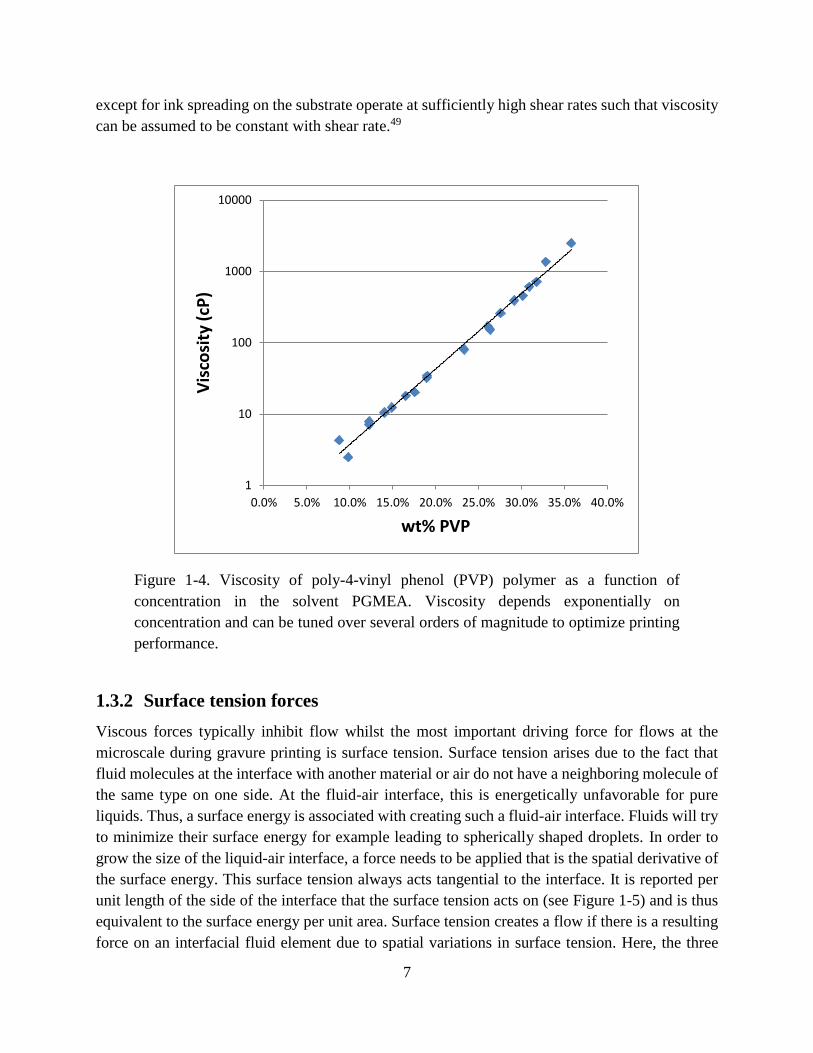
7
except for ink spreading on the substrate operate at sufficiently high shear rates such that viscosity
can be assumed to be constant with shear rate.49
Figure 1-4. Viscosity of poly-4-vinyl phenol (PVP) polymer as a function of
concentration in the solvent PGMEA. Viscosity depends exponentially on
concentration and can be tuned over several orders of magnitude to optimize printing
performance.
1.3.2 Surface tension forces
Viscous forces typically inhibit flow whilst the most important driving force for flows at the
microscale during gravure printing is surface tension. Surface tension arises due to the fact that
fluid molecules at the interface with another material or air do not have a neighboring molecule of
the same type on one side. At the fluid-air interface, this is energetically unfavorable for pure
liquids. Thus, a surface energy is associated with creating such a fluid-air interface. Fluids will try
to minimize their surface energy for example leading to spherically shaped droplets. In order to
grow the size of the liquid-air interface, a force needs to be applied that is the spatial derivative of
the surface energy. This surface tension always acts tangential to the interface. It is reported per
unit length of the side of the interface that the surface tension acts on (see Figure 1-5) and is thus
equivalent to the surface energy per unit area. Surface tension creates a flow if there is a resulting
force on an interfacial fluid element due to spatial variations in surface tension. Here, the three
1
10
100
1000
10000
0.0% 5.0% 10.0% 15.0% 20.0% 25.0% 30.0% 35.0% 40.0%
Vis
cosi
ty (
cP)
wt% PVP
8
main forms of such spatial variations that are encountered during printing are reviewed: curved
fluid interfaces that lead to spatial variations in the surface tension force vector, variations in
surface tension magnitude and variations due to the presence of multiple disparate interfaces.
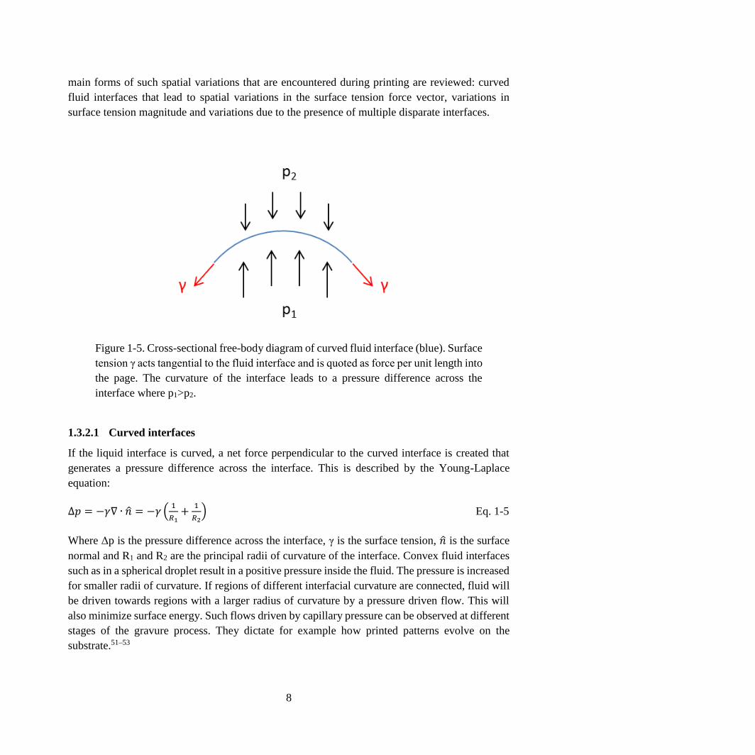
Figure 1-5. Cross-sectional free-body diagram of curved fluid interface (blue). Surface
tension γ acts tangential to the fluid interface and is quoted as force per unit length into
the page. The curvature of the interface leads to a pressure difference across the
interface where p1>p2.
1.3.2.1 Curved interfaces
If the liquid interface is curved, a net force perpendicular to the curved interface is created that
generates a pressure difference across the interface. This is described by the Young-Laplace
equation:
∆𝑝 = −𝛾∇ ∙ �� = −𝛾 (1
𝑅1+
1
𝑅2) Eq. 1-5
Where Δp is the pressure difference across the interface, γ is the surface tension, �� is the surface
normal and R1 and R2 are the principal radii of curvature of the interface. Convex fluid interfaces
such as in a spherical droplet result in a positive pressure inside the fluid. The pressure is increased
for smaller radii of curvature. If regions of different interfacial curvature are connected, fluid will
be driven towards regions with a larger radius of curvature by a pressure driven flow. This will
also minimize surface energy. Such flows driven by capillary pressure can be observed at different
stages of the gravure process. They dictate for example how printed patterns evolve on the
substrate.51–53

9
1.3.2.2 Surface tension gradients
The second mechanism by which surface tension induces flow is spatial variations in the
magnitude of surface tension, termed Marangoni flow. Surface tension depends on a number of
variables. The most immediate variable is the type of fluid. In complex inks such as those
encountered in printed electronics with at least two components (solvent and solute), surface
tension depends on composition. Especially solutes that act as surfactants by preferentially
organizing on the fluid surface can dramatically lower surface tension. Another important variable
that determines the magnitude of a fluid’s surface tension is temperature. Surface tension decreases
with increasing temperature until tending to zero at the boiling point. Thus, spatial variations in
solute concentration or temperature can result in surface tension gradients and induce flow. One
important situation where gradients in both of these variables can be observed is during ink drying
on the substrate after printing. During drying, the liquid solvent evaporates leaving the solute
behind. Viscosity increases until it is large enough to prevent any further flow and the final dry
shape has been reached. Solvent evaporation requires energy that can locally lower the fluid
temperature where the evaporation rate is highest leading to temperature gradients. Concentration
gradients can be created due to convective flows during drying. For example, since solvent
evaporation is fastest at the edges of patterns, a convective flow is created from the inside of the
pattern to its perimeter. Significant amounts of solute material can be deposited at the rim of
patterns leading to very non-uniform thickness profiles (see Figure 1-6). This is the so-called
coffee ring effect. This problem is more pronounced in inkjet printing but can also be observed
when low-viscosity inks are printed by gravure. It can be mitigated by understanding and balancing
the temperature and concentration gradient induced Marangoni flows with the outward convective
flow.54–57
10
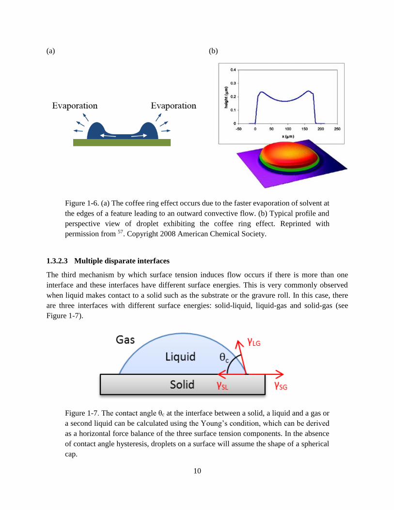
(a) (b)
Figure 1-6. (a) The coffee ring effect occurs due to the faster evaporation of solvent at
the edges of a feature leading to an outward convective flow. (b) Typical profile and
perspective view of droplet exhibiting the coffee ring effect. Reprinted with
permission from 57. Copyright 2008 American Chemical Society.
1.3.2.3 Multiple disparate interfaces
The third mechanism by which surface tension induces flow occurs if there is more than one
interface and these interfaces have different surface energies. This is very commonly observed
when liquid makes contact to a solid such as the substrate or the gravure roll. In this case, there
are three interfaces with different surface energies: solid-liquid, liquid-gas and solid-gas (see
Figure 1-7).
Figure 1-7. The contact angle θc at the interface between a solid, a liquid and a gas or
a second liquid can be calculated using the Young’s condition, which can be derived
as a horizontal force balance of the three surface tension components. In the absence
of contact angle hysteresis, droplets on a surface will assume the shape of a spherical
cap.

11
The contact angle that the liquid-gas interface makes to the solid surface (assumed to be flat here)
depends on the balance between these three surface energies as given by the Young’s equation:
cos 𝜃𝑐 =𝛾𝑆𝐺−𝛾𝑆𝐿
𝛾𝐿𝐺 Eq. 1-6
Where θc is the contact angle, γ denotes surface energy and S, G and L denote solid, gas and liquid
respectively. If γSG – γSL > γLG, the contact angle will be zero and the liquid will spread
uncontrollably to form a thin film. This situation of total wetting occurs for example in the case of
water on clean silicon dioxide. If 𝛾𝑆𝐺−𝛾𝑆𝐿
𝛾𝐿𝐺 is between 0 and 1, the liquid partially wets the solid.
The contact angle will lie between 0 and 90 degrees. This is a common situation found in printed
electronics for example in the case of many organic solvents on plastic substrates after their surface
energy was increased using methods such as oxygen plasma treatment. Such contact angles are
often desirable because the ink will spread on the surface to form a uniform film without spreading
uncontrollably thereby making effective patterning impossible. If γSG – γSL < 0, the ink will not
wet the solid surface and make a contact angle larger than 90 degrees. For example, many
fluorinated polymers such as Teflon have sufficiently low surface energy to be non-wetting. This
situation can be desirable to prevent ink from flowing onto certain surfaces such as the doctor
blade during gravure printing. However; in the context of substrates to be printed on, non-wetting
surfaces are generally undesirable because they tend to cause patterns to break up and ink to ball
up to minimize surface energy. In the context of aqueous inks, surfaces with contact angle below
90 degrees are termed hydrophilic and surfaces with contact angle above 90 degrees are termed
hydrophobic. This analysis assumes that there is one unique equilibrium contact angle. However,
in most real situations this is not the case. Usually, there exists a range of contact angles that are
stable. The advancing contact angle marks the upper end of this range. If the contact line reaches
this angle, for example because more fluid is added to a droplet on a surface, the contact line will
advance i.e. the fluid will spread further on the surface. The receding contact angle marks the lower
end of the equilibrium range. If the contact line reaches this angle, for example because fluid is
removed from a droplet on a surface, the contact line will recede i.e. the droplet will shrink. This
contact angle hysteresis can be caused by microscale roughness or chemical inhomogeneity of the
surface. The contact line gets pinned at such variations in equilibrium contact angle as it moves
across the surface. Contact angle hysteresis can be exploited to print patterns on a substrate that
would be impossible to print if there was only one equilibrium contact angle such as features with
sharp corners.53
More complex situations with more than three interfaces exist, driving fluid flow. For example, if
there are two different solids in contact with a liquid, the liquid will flow towards the surface with
the higher surface energy i.e. lower contact angle. This is the case in the gravure process during
doctor blade wiping where the ink is in contact with the doctor blade and the roll or during ink
transfer from the roll to the substrate where the ink is in contact with the roll and the substrate.

12
These situations will be described in detail in the next section. In these situations, it is crucial to
be able to control the contact angle of an ink on the substrate or other components such as the
gravure roll or doctor blade. There are a number of ways in which this can be achieved. One way
would be to change the surface energy of the ink. This can be achieved by changing the ink solvent,
by changing the solute concentration or type or by adding a surfactant. One challenge with these
ink based methods is that they can dramatically alter the properties of the final film and its
electrical properties. Additionally, in situations with multiple solid interfaces, it is often
advantageous to modify the surface energies of different solids independently. Modifications of
the solid surface are thus much more common. Contact angle is typically decreased using UV
ozone (UVO) or plasma treatments that remove organic contaminants and activate the surface. The
contact angle can be increased by depositing self-assembled monolayers (SAM) on the surface.58
By choosing the right functional groups, surface energy can be tuned, for example employing
fluorinated end groups to achieve contact angles above 90 degrees. Contact angle hysteresis can
be reduced by using very smooth substrates that have been cleaned thoroughly to remove any
contamination. Conversely, contact angle hysteresis can be increased by intentionally roughening
the surface or introducing intentional chemical inhomogeneity.
In summary, the most important forces for microscale printing are viscous and surface tension
forces. Their balance is captured by the capillary number. Understanding viscous as well as surface
tension effects allows printing to be optimized by the careful tuning of ink as well as printing and
surface parameters. The next section describes how this understanding can be applied to gravure
printing in particular.
1.4 Overview of gravure printing process
The physics of the gravure printing process underpins many of the findings of this thesis and is
thus reviewed here. Many of the processes that affect ink distribution can be understood in terms
of the fluid mechanics described in the previous section, namely flows driven by surface tension
forces and inhibited by viscous forces. The gravure process can be considered a series of sub-
processes (see Figure 1-3).49 First, ink needs to fill the cells. In continuous production, the roll
typically rotates through a large ink reservoir, filling the cells. Afterwards, ideally, the cells are
fully filled with ink without any entrapped air. Additional ink will be left on the land areas between
cells and there will also be excess ink on top of the cells. This excess ink is removed using a doctor
blade. Afterwards, ideally, there is no ink left on the land areas and cells are still fully filled with
ink. In reality, there is always a thin lubrication residue film left by the finite gap between the blade
and the roll. The blade will also pull ink from the cells and redeposit it behind the cells in the form
of characteristic drag-out tails. After wiping, the roll is pressed into contact with the substrate.
Ideally, all the ink is removed from the cells and transferred onto the substrate. Finally, the ink
13
needs to spread on the substrate to fill in the gaps in between individual cells. All of these effects,
except for spreading, can initially be analyzed in terms of individual, isolated cells. Initially, they
can also be understood as independent processes. An ideality factor can be calculated for each sub-
process. The ideality factor describes the volume of ink in the cell or on the substrate respectively
after the filling, wiping and transfer processes. The final printed volume fraction is simply the
product of these individual ideality factors:
𝜑𝑝𝑟𝑖𝑛𝑡 =𝑉𝑡𝑟𝑎𝑛𝑠𝑓𝑒𝑟
𝑉𝑐𝑒𝑙𝑙=
𝑉𝑓𝑖𝑙𝑙
𝑉𝑐𝑒𝑙𝑙×
𝑉𝑤𝑖𝑝𝑒
𝑉𝑓𝑖𝑙𝑙×
𝑉𝑡𝑟𝑎𝑛𝑠𝑓𝑒𝑟
𝑉𝑤𝑖𝑝𝑒= 𝜑𝑓𝑖𝑙𝑙𝜑𝑤𝑖𝑝𝑒𝜑𝑡𝑟𝑎𝑛𝑠𝑓𝑒𝑟 Eq. 1-7
The dominant factor controlling these ideality factors is the capillary number. The different sub-
processes in gravure exhibit different dependencies on Ca. Different regimes of capillary number
are limited by different sub-processes (see Figure 1-16). Knowledge of these different printing
regimes is crucial when optimizing a new printing process in terms of ink design, substrate
treatment and print speed.
1.4.1 Cell filling
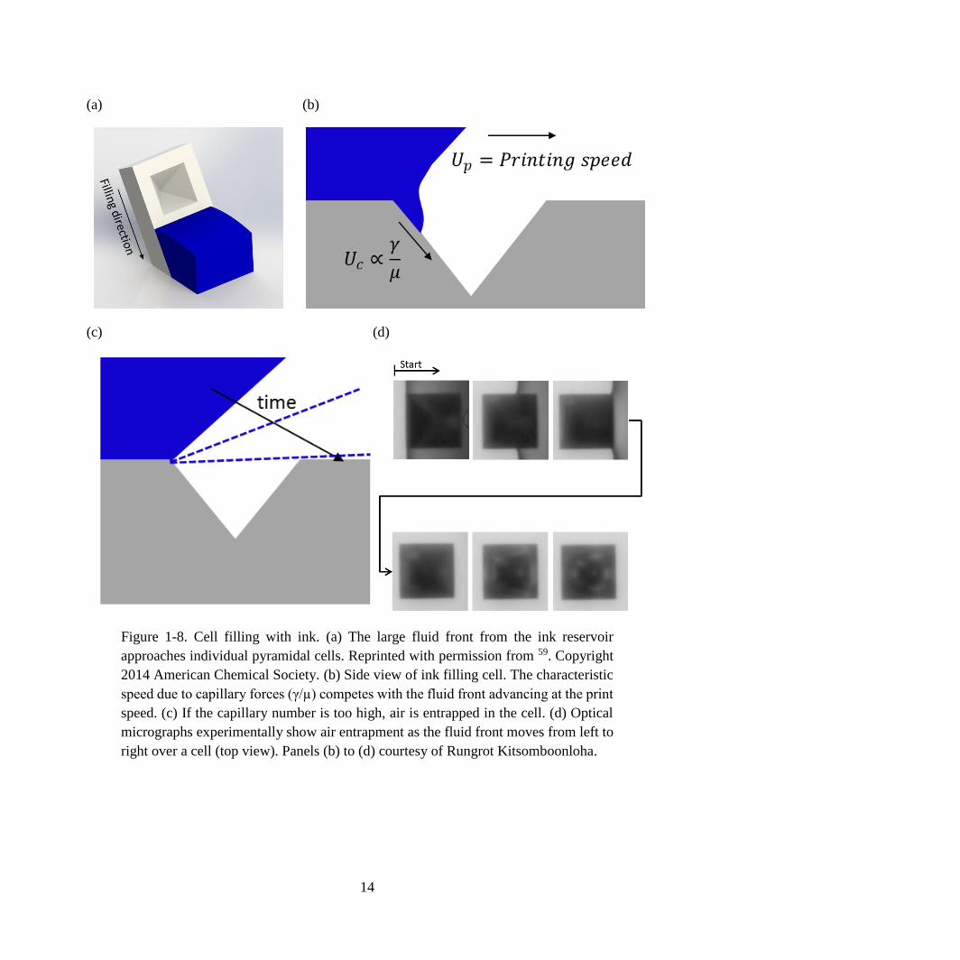
The first process during gravure printing is cell filling. In this process, ink replaces the air initially
within each cell, thus filling the cells. Air entrapment is the biggest problem during cell filling.
Ideally, the cell is fully filled with ink afterwards. Ink from a large reservoir enters the cell as a
large fluid front passes over the cell (see Figure 1-8). As the fluid front approaches the cell, it gets
pinned at the edge of the cell. Due to the declining angle of the cell wall, the contact angle is
reduced at the edge of the cell. The liquid front will remain pinned until the contact angle becomes
larger than the advancing contact angle of the ink on the roll surface. At this point, ink will be
driven into the cell by surface tension forces. At the same time, the overall fluid front keeps
advancing around the edges of the cell and ultimately over the cell. If the ink has not fully filled
the cell when the overall fluid front hits the cell’s trailing edge, air will be entrapped inside the
cell.59–62 Thus, the success of cell filling is decided by two competing processes. The overall fluid
front moves at the print speed. The velocity of the fluid entering the cell is determined by the
balance of surface tension and viscous forces. Lower viscosity and larger surface tension result in
faster and more complete filling of the cell. To first order, capillary number determines the filled
volume fraction. Large values of Ca mean the overall fluid front moves faster relative to the ink
filling the cell. Thus, filling will be incomplete at large values of Ca and the ideality factor will be
small.
14
(a) (b)
(c) (d)
Figure 1-8. Cell filling with ink. (a) The large fluid front from the ink reservoir
approaches individual pyramidal cells. Reprinted with permission from 59. Copyright
2014 American Chemical Society. (b) Side view of ink filling cell. The characteristic
speed due to capillary forces (γ/µ) competes with the fluid front advancing at the print
speed. (c) If the capillary number is too high, air is entrapped in the cell. (d) Optical
micrographs experimentally show air entrapment as the fluid front moves from left to
right over a cell (top view). Panels (b) to (d) courtesy of Rungrot Kitsomboonloha.
15
1.4.2 Doctor blade wiping
The doctor blade is a component that sets gravure apart from most other printing techniques. It is
needed because large amounts of fluid are left on the land areas after the filling process. Ideally,
the doctor blade wipes off all excess ink without affecting the ink in the cell. Unfortunately, two
major non-idealities occur during doctor blade wiping: homogeneous lubrication residue and ink
drag-out from cells.
1.4.2.1 Lubrication residue
When the doctor blade passes over the roll surface, it always leaves a thin, uniform residue layer.
The fluid moves with the roll as it rotates until the fluid hits the doctor blade. The convergent gap
underneath the doctor blade forms a thin channel. In order to achieve a constant flow rate through
the channel, a positive pressure is developed underneath the blade. This pressure is balanced by
the loading force that is applied to the top of the blade mount (see Figure 1-9). The thickness of
the uniform residue layer is controlled by several parameters; however, it can never be avoided
completely. Depending on the application, different residue thicknesses can be acceptable. If the
residue is very thick, it can lead to electrical shorts between different parts of a circuit when a
conducting ink is printed. Electrical shorts can be avoided if the residue is thin enough such that
individual nanoparticles from a metal nanoparticle ink do not form a continuous layer after
sintering. The particular thickness at which this happens depends on the nanoparticle size, mass
loading and sintering conditions. Thin, sensitive layers printed on top of the residue film can be
affected by the surface roughness that even discontinuous residue films can produce. It is well
known that roughness can lead to dielectric failure 63 as well as crystallization defects in
semiconductors 64,65. Excessive residue can also lead to hazing and degraded transparency of
transparent substrates for optical applications. The residue thickness can be reduced by the
optimization of ink, printing and doctor blade conditions.66,67 Both a reduced ink viscosity and a
reduced print speed result in lower pressures in the gap underneath the doctor blade and thus
thinner films (see Figure 1-10). In the high capillary number regime, printed volume fraction
increases due to large amounts of residue. Since this residue is deposited uniformly over the roll
surface, the patterning contrast decreases at high values of Ca and thus the increase in printed
volume fraction is undesirable. Thus, printing with low viscosity inks and at low speeds is desirable
from a lubrication residue perspective.

16
(a) (b)
Figure 1-9. Lubrication residue due to doctor blade wiping. (a) Mounting of the doctor
blade. The doctor blade can move freely in the vertical direction with an applied
vertical load. (b) Lubrication residue is created by ink flowing through the finite gap
that always exists underneath the doctor blade. Courtesy of Rungrot Kitsomboonloha.
Figure 1-10. Lubrication residue improves for smaller values of print speed and
viscosity (𝑈∗ =𝜇𝑈
𝑅𝐸′). Reprinted with permission from 66. Copyright 2014 American
Chemical Society.
17
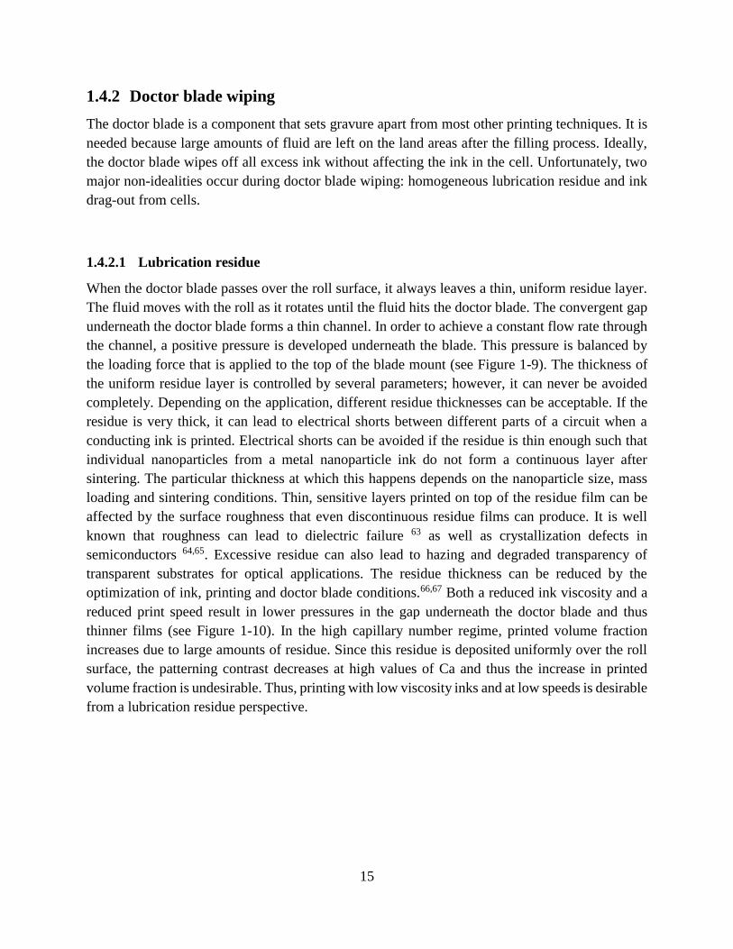
1.4.2.2 Drag-out
The second major non-ideality during doctor blade wiping is drag-out. Whilst lubrication residue
occurs uniformly across the roll surface, drag-out is a result of the interaction between the doctor
blade and the cells. The doctor blade pulls out ink from the cells as it passes over them, which has
two detrimental consequences: ink is lost from the cells and subsequently redeposited behind the
cells. The redeposited ink behind the cells takes the form of characteristic tails, which are generally
undesirable because pattern fidelity is deteriorated. The drag-out effect can be explained based on
the wettability of the ink on the doctor blade. Kitsomboonloha et al. use experimental results to
propose that a 3D capillary effect is responsible for drag-out (see Figure 1-11).49 As the doctor
blade passes over the cell, the ink meniscus underneath the doctor blade will be larger in the cell
compared with adjacent land areas. A pressure gradient is created that drives liquid from the cell
onto adjacent land areas, both sideways and towards the backside of the doctor blade. The sideways
flow is evident from the shape of the drag-out tail whose width extends past the boundaries of the
cell (see Figure 1-12). Ceyhan et al. use lubrication theory to analyze the drag-out effect in 2D
considering the blade cross-section.68 It is shown that the ink climbs up the backside of the doctor
blade to be pulled out of the cell and to be redeposited as a tail behind the cell. In both cases, the
drag-out effect is described by a capillary flow, which is suppressed at higher capillary numbers.
At high capillary numbers, there is insufficient time for the ink to be dragged out because the print
speed is too high relative to the characteristic velocity of the capillary flow (γ/µ). Thus, the printed
volume fraction is limited by drag-out at low values of Ca (see Figure 1-12).
(a) (b)
Figure 1-11. The drag-out process. (a) Ink is pulled from the cell as the doctor blade
passes over it. Ink wets the blade and flows both sideways under the blade and up the
backside of the blade. After the blade has passed over the cell, the dragged-out ink is
redeposited on the land area behind the cell. (b) Standard blade tips are significantly
larger than the size of highly-scaled cells. They can be modelled as cylinders that
create a very shallow angle wedge at the very tip. This small wedge leads to the
capillary flow of ink from the cell. Courtesy of Rungrot Kitsomboonloha.
18
Figure 1-12. Both the width and length of the resulting drag-out tails decrease with
increasing capillary number because capillary flow is suppressed in this regime.
Reprinted with permission from 49. Copyright 2012 American Chemical Society.
1.4.3 Ink transfer
The final process involving the roll is ink transfer to the substrate. The substrate comes in contact
with the ink on the roll. When the two are separated, ideally, all the ink has been removed from
the cells and transferred to the substrate. In reality, transfer fractions tend to be much lower than
100%. Ink transfer is the most extensively studied gravure sub-process, both experimentally and
theoretically,69–80 as described in a recent review article by Kumar.81 During the transfer process,
a liquid bridge is created between the roll and the substrate (see Figure 1-13). The breakup of this
liquid bridge determines what fraction of ink is left on the roll and what fraction is transferred to
the substrate. Initial understanding can be gained by studying the breakup of liquid bridges
between two flat plates. If both plates have the same wetting properties, the contact line will slip
by the same amount on both plates such that both plates end up with the same amount of fluid after
breakup. If the two plates exhibit different receding contact angles, the movement of the contact
lines will not be symmetric anymore. The contact line will de-pin faster on the plate with a higher
receding contact angle. After break-up, this plate will be left with a smaller fraction of ink.75 The
same considerations apply to the transfer from a cell to a flat substrate.77 This effect is driven by
surface tension forces. At high values of capillary number, viscous forces dominate over surface
19
tension forces. In this case, the wetting difference between the two plates becomes less important
and the liquid will be split more evenly. Thus, the value of capillary number that gives optimum
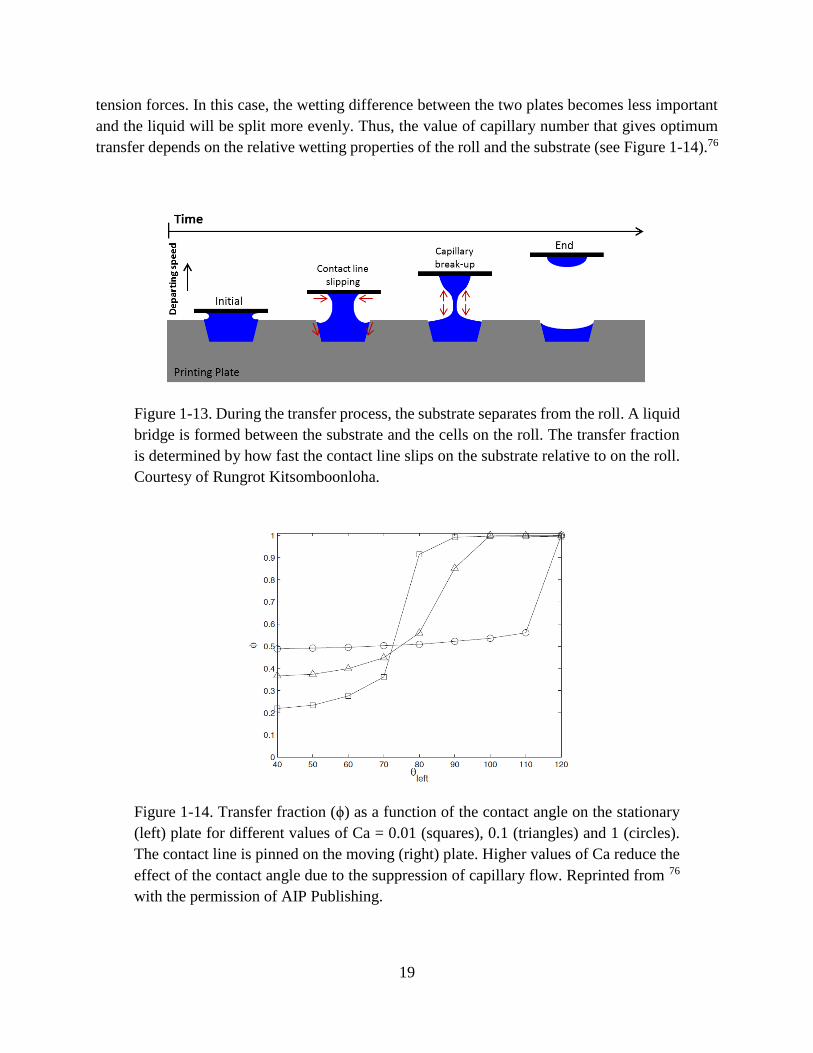
transfer depends on the relative wetting properties of the roll and the substrate (see Figure 1-14).76
Figure 1-13. During the transfer process, the substrate separates from the roll. A liquid
bridge is formed between the substrate and the cells on the roll. The transfer fraction
is determined by how fast the contact line slips on the substrate relative to on the roll.
Courtesy of Rungrot Kitsomboonloha.
Figure 1-14. Transfer fraction (ϕ) as a function of the contact angle on the stationary
(left) plate for different values of Ca = 0.01 (squares), 0.1 (triangles) and 1 (circles).
The contact line is pinned on the moving (right) plate. Higher values of Ca reduce the
effect of the contact angle due to the suppression of capillary flow. Reprinted from 76
with the permission of AIP Publishing.

20
1.4.4 Pattern formation on the substrate
So far, we have discussed the individual gravure sub-processes that involve cells on the roll,
namely filling, wiping and transfer. These processes can mostly be understood in the context of
individual cells. However, virtually all realistic electronic applications consist of multiple cells
that form a continuous pattern by ink spreading on the substrate. Thus, ink spreading and drying
are processes that need to be discussed in the context of pattern formation. The most basic patterns
for electronic applications are lines and rectangles, since virtually all electronic patterns including
transistor gates and source/drain electrodes, interconnects, capacitors, etc., are constructed out of
these basic primitives. Since gravure is a cell based printing method, the desired patterns are
pixelated into individual cells (see Figure 1-15). For example, high-resolution lines are typically
made up of a string of individual cells. During transfer, the ink is deposited on the substrate in the
form of individual droplets. These droplets need to spread to fill in the gaps between individual
cells and create a continuous pattern. The final pattern shape depends on both the driving force
towards equilibrium, which is surface energy, as well as the timescale available to reach
equilibrium. The merging of adjacent droplets is driven by surface energy minimization. Clearly,
this depends on both the surface energies of the ink and the substrate. The equilibrium shape can
range from de-wetting where individual droplets ball up to complete spreading where pattern
definition is lost. Intermediate contact angles are needed to achieve good pattern fidelity. This flow
is inhibited by viscous forces. Highly viscous inks (viscosities above a few hundred centipoise)
are very challenging to print with gravure because they result in isolated droplets that do not spread
sufficiently. This will be observed multiple times in this thesis and will be discussed in the
following chapters. The timescale available for droplet spreading is limited by the drying of the
solvent. As the solvent dries, viscosity increases and spreading ultimately stops.
(a) (b)
Figure 1-15. (a) Gravure patterns such as these source drain lines with contact pads
are subdivided into individual cells. (b) Ink deposited from individual cells needs to
spread on the substrate to create continuous patterns. (a) and (b) reprinted with
permission from 27.
21
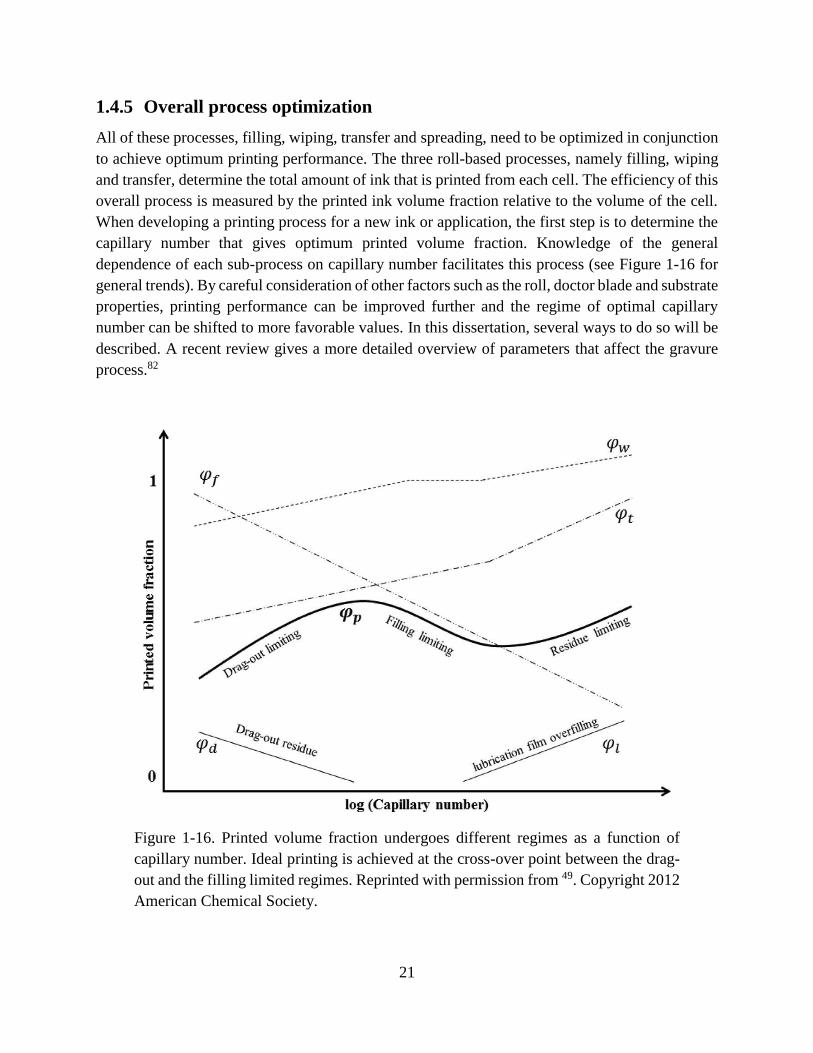
1.4.5 Overall process optimization
All of these processes, filling, wiping, transfer and spreading, need to be optimized in conjunction
to achieve optimum printing performance. The three roll-based processes, namely filling, wiping
and transfer, determine the total amount of ink that is printed from each cell. The efficiency of this
overall process is measured by the printed ink volume fraction relative to the volume of the cell.
When developing a printing process for a new ink or application, the first step is to determine the
capillary number that gives optimum printed volume fraction. Knowledge of the general
dependence of each sub-process on capillary number facilitates this process (see Figure 1-16 for
general trends). By careful consideration of other factors such as the roll, doctor blade and substrate
properties, printing performance can be improved further and the regime of optimal capillary
number can be shifted to more favorable values. In this dissertation, several ways to do so will be
described. A recent review gives a more detailed overview of parameters that affect the gravure
process.82
Figure 1-16. Printed volume fraction undergoes different regimes as a function of
capillary number. Ideal printing is achieved at the cross-over point between the drag-
out and the filling limited regimes. Reprinted with permission from 49. Copyright 2012
American Chemical Society.

22
1.5 Printed organic thin-film transistors (OTFTs)
So far, the printing of different patterns and layers one at a time has been discussed. In real printed
electronics, multiple functional layers need to be combined to create devices. Gravure printing has
been used to print a multitude of devices such as OLEDs35 and organic solar cells34. This
dissertation will focus on printed transistors. Transistors are technologically very important as
most printed systems will include transistors to perform tasks such as digital logic, signal
amplification in sensors or pixel selection in displays. Transistors are also a good testbed for a new
microfabrication technology because they combine a number of different requirements. High-
quality transistors require both the lateral downscaling of feature size as well as the thickness
downscaling of highly-uniform layers. Conductors, dielectrics and semiconductors all need to be
printed as high-quality materials. Interactions between the different layers are very important both
in terms of printing, e.g. solvent compatibility and wetting, and in terms of electronic interfaces,
e.g. contact resistance and interfacial trap states. All of these problems need to be solved to create
viable fully-printed devices (see device geometry in Figure 1-17).
Figure 1-17. Cross-section of fully-overlapped TFT architecture showing all four
layers: source (S) and drain (D) electrodes, semiconductor, gate dielectric and gate
electrode (G). The interfaces between all layers need to be compatible. The
semiconductor and dielectric layer thicknesses need to be scaled i.e. made thin to
ensure good electrostatic integrity. The source and drain layer lateral dimensions need
to be scaled to ensure good on-state performance both due to a short channel length as
well as a small overlap capacitance between the gate and the source and drain
electrodes with small linewidth.
There are a number of requirements on transistor performance that determine its viability. In the
on-state, transistors are required to drive as much on-current as possible without requiring a large
supply voltage. A large drive current is needed to increase the maximum switching frequency for
many high-frequency applications. The transition frequency fT is defined as the frequency at which
the transistor current gain becomes unity and the transistor ceases to work as a voltage controlled
switch. Recently, a number of reports have demonstrated printed transistors with fT in the range of
hundreds of kHz to low MHz.15,18,83,23,27 However, in these cases, the devices were either not fully
printed, especially high-speed printed, and/or were operating at large voltages above 10V, which
23
increases fT as can be seen from the following calculation based on the small-signal equivalent
transistor circuit:
𝑓𝑇 =𝑔𝑚
2𝜋(𝐶𝑔𝑠+𝐶𝑔𝑑)=
𝜇(𝑉𝐺𝑆−𝑉𝑇)
2𝜋𝐿(23
𝐿+2𝐿𝑜𝑣𝑒𝑟𝑙𝑎𝑝) Eq. 1-8
Where µ is mobility, VGS is the applied gate-source voltage, VT is the threshold voltage, L is the
channel length and Loverlap is the overlap length between the gate and the source and drain
electrodes. Thus, fT can be improved by improving mobility and by reducing channel length and
overlap capacitance.
Mobility is a material property. It depends on both the semiconductor material as well processing
conditions. Organic materials are the most widely explored class of materials for printed
transistors.12–21,25,26,24 Traditionally, the performance of organic semiconductors has been very
low. However, recently, novel solution processed organic semiconductor materials have boosted
performance considerably achieving mobilities in excess of 1cm2/V-s and in some cases even
10cm2/V-s.84,85 A novel scanned annealing method is presented in this dissertation that increases
mobility by an order of magnitude.26 However, the main advantage of organic materials is their
properties that make them attractive for printing processes on plastic substrates. Organic materials
can be readily dissolved in a large range of organic solvents that allow fine control over parameters
such as ink viscosity or evaporation rate, which are critical to achieve optimal patterning and layer
uniformity. Annealing temperatures are typically very low on the order of 100°C. This is a major
advantage because it enables the use of low-cost, flexible substrates such PET, PEN or paper.
Whilst the semiconductor is certainly a key component of any transistor, materials for the other
layers also need to be chosen carefully. Organic materials can also be used for the dielectric with
the same advantages in terms of printability as organic semiconductors. Organic thin-film
transistors (OTFTs) typically utilize metal nanoparticle inks for the source, drain and gate
electrodes due to their good conductivity, printability and low processing temperatures that are
matched to the thermal limits of the organic materials.9 Many of the advances in OTFT materials,
especially the semiconductor, have been obtained using idealized structures such as silicon
substrates, evaporated contacts or spin coated layers. The next step is to employ these high-
performance organic materials in devices where every layer is patterned by printing at high speed.
In addition to improvements in material mobility, downscaling of the source, drain and channel
dimensions is the second way to improve transistor high-frequency performance. A number of
reports have focused on the printing of transistor electrodes with scaled lateral feature dimensions,
using a range of different printing methods.16,18,23,27,25,28 As discussed earlier, gravure printing
offers a promising path towards the scalable high-speed printing of downscaled feature
dimensions. One major challenge for gravure printed devices is that layer-to-layer registration
24
accuracy has lagged behind improvements in resolution, which severely limits the downscaling of
the overlap length and thus overlap capacitance. A significant overlap capacitance severely limits
fT as is evident from Eq.1–8. An early solution employed a hybrid approach where a scaled gate
electrode was gravure printed and aligned source and drain electrodes were printed using
inkjet.23,83,86 As resolution is scaled further, this technique reaches its limit in terms of accuracy of
the inkjet printing especially at high printing speeds. Self-aligned printing is another potential
solution to limit overlap capacitance analogous to self-aligned photolithography. Differences is
wetting behavior are exploited to guide the ink to a desirable location without the need for top-
down alignment. This approach has been applied to create very small gaps between source and
drain electrodes.87–89 However, self-alignment of source and drain electrodes to the gate through
the gate dielectric still remains challenging.17 Gravure printing enables another route towards high-
frequency operation by not only scaling the channel length but also the linewidth of electrodes.
This limits overlap capacitance even if a fully-overlapped gate is employed that is much larger
than the combined channel length and the width of the two electrodes (see Figure 1-17). Thus,
requirements for alignment accuracy can be relaxed. Since the conductivity of printed metallic
conductors is typically not the limiting factor in printed organic transistor performance, deleterious
effects of the series resistance of the narrow source/drain lines are minimal. This has been
demonstrated with an inkjet printed gate fully-overlapped with gravure printed source/drain
electrodes thus creating a path towards high-frequency transistors based on highly-scaled gravure
printed source and drain electrodes.27 In this dissertation, transistors are demonstrated where the
fully-overlapped gate is gravure printed. In addition, the semiconductor and the dielectric are also
gravure printed. Thus, all transistor layers are printed at a high speed of 1m/s enabling high-
throughput manufacturing. By scaling all layers and optimizing printing processes, high-
performance, low-voltage devices are demonstrated with low variability.28
1.6 Thesis organization
In this thesis, gravure printing is advanced on several levels with the goal to create fully gravure
printed devices. First, gravure is used to prepare paper substrates for printed electronics. Then,
single-layer printing for highly-scaled device features is discussed in terms of roll tooling as well
as pattern formation. Finally, multi-layer printing is demonstrated in fully gravure printed
transistors.
In chapter 2, gravure printing is utilized to enable the printing of transistors on a novel substrate:
paper. Paper is very attractive for printed electronics because it is low-cost, biodegradable,
lightweight and ubiquitous. However, its porosity causes ink absorption and large surface
roughness. This is overcome by a gravure printed local smoothing layer. Printed transistors on top
of locally smoothed paper substrates are demonstrated that exhibit performance on-par with

25
previously reported devices on plastic substrates; however, these devices were not fully gravure
printed yet.
In chapter 3, a novel fabrication process for gravure rolls is demonstrated to enable gravure printing
of highly-scaled devices. By utilizing the strengths of silicon microfabrication, gravure rolls can
be fabricated that have superior feature definition as well as superior surface finish compared with
traditional gravure roll making techniques, especially for high-resolution features. Modifications
of the roll surface properties allow tuning of the printing performance to print high-resolution
patterns at high print speeds.
In chapter 4, such highly-scaled gravure printed features are analyzed more closely. More complex
patterns than single lines or cells are printed. Proximity effects are demonstrated that occur when
lines are printed close to each other. The fluid mechanics of this effect is studied and it is suggested
how it can be used to enhance feature quality by employing assist features.
In chapter 5, multi-layer printing for printed organic thin-film transistors (OTFTs) is demonstrated.
In the first part of the chapter, a novel scanned thermal annealing technique is presented that
significantly improves the crystallization of an organic semiconductor. The separation of grain
nucleation and growth leads to increased grain size and significantly improved electrical
performance. In the second part of the chapter, transistors are fully gravure printed at a high print
speed of 1m/s. By scaling both lateral and thickness dimensions and optimizing the printing
processes, good electrical performance, low-voltage operation and low variability is demonstrated.
In chapter 6, the main findings of this thesis are summarized and future research directions are
suggested.

26
Chapter 2: Gravure printing enabled transistors on novel
paper substrates
2.1 Introduction
Paper is one of the most ubiquitous materials in everyday life. It has been used for centuries to
display printed information in addition to other applications. The reasons are manifold including
the low cost of paper itself, the ability for high-throughput, low cost printing on paper,
biodegradability, permeability, foldability and many more. There will be countless opportunities
if these properties can be integrated with electronic functionalities. One of the most immediate
applications is the integration of sensing, communication and display functionalities with paper
consumer packaging. This cannot be achieved with traditional microfabrication; however, the
advent of printed electronics offers the opportunity to close this gap. So far, the majority of the
advances in printed electronics have been made on plastic substrates. Little progress has been made
on paper. The largest roadblocks preventing this are the surface roughness and ink absorption due
to the porosity of paper.90 High-resolution printing methods such as inkjet and gravure rely on
relatively low viscosity inks, which are absorbed by standard paper. Higher viscosity inks cannot
be printed by inkjet. They can be printed by gravure; however, fine lines printed with gravure
directly onto paper would still suffer substantially from the large roughness of paper. So far, this
has prevented any fully printed devices or systems, compatible with paper packaging flows, from
being demonstrated.
One previous approach has been to “hide” the paper under a blanket coating of a smooth material;
coating methods such as spin coating91–93 and parylene evaporation94–96 have been used to deposit
thick smoothing layers. Unfortunately, such approaches are not viable for real packaging
applications since all the attractive mechanical properties of paper, such as foldability,
breathability etc., are lost when coated with blanket sealing layers. It is also undesirable from a
cost perspective since large areas of paper are unnecessarily coated, wasting large quantities of
material. Further, other previous work has made use of coated “inkjet paper” substrates97, which
are too expensive for use in consumer product packaging and don’t have sufficient thermal stability
for some higher temperature fabrication processes. There have also been reports of devices
fabricated directly on paper. This is mostly done by conventional micro fabrication techniques
such as sputtering or vacuum deposition thereby avoiding the problem of ink absorption into paper
during printing.98,99 Whilst this might be viable for some niche applications such as security
features on banknotes, it won’t meet the cost requirements of most applications of paper
electronics. Direct printing on paper using screen printing has also been attempted, however, with
relatively large channel lengths (200µm),100 which highlights the challenges involved in the scaling
of printed transistors on rough paper. This can be acceptable for certain applications such as low
resolution electrothermochromic displays.101 However, most electronic applications will require
27
high-resolution printing of scaled transistors. The shortcomings of the current state-of-the-art in
terms of paper-based transistors become especially evident when comparing them to the state-of-
the-art in terms of printed transistors on plastic substrates. On plastic substrates, transistors have
been demonstrated where multiple if not all layers were fabricated by printing methods. Especially
gravure printed transistors have been very successful at scaling down the channel length below
10µm whilst achieving good performance.24,16,18,23,27,25,28 Overall, therefore, existing paper-based
processes and techniques are generally not viable, since they are incompatible with conventional
packaging flows, which make use of printing techniques and run in high-speed roll-to-roll
processes on low-cost paper stock.
These challenges are overcome by the integrated process flow demonstrated in this chapter.22 A
smoothing underlayer as well as overlying transistors are printed on low-cost paper using gravure
printing. Gravure printing is widely used in the graphic arts, and therefore, this work is a natural
evolution of consumer product packaging to integrate printed transistors. The smoothing layer is
printed locally as defined by the pattern on the gravure roll. This preserves the desirable properties
of paper outside of the electronically active areas, which can be a small fraction of the overall size
of the paper. Interconnects between multiple smoothed regions with high performance devices
could then be fabricated by methods such as screen printing, or indeed, using lower-resolution
gravure printing of more viscous (and thus less absorbed) conductor inks, since high-resolution
printing would be less of a concern.
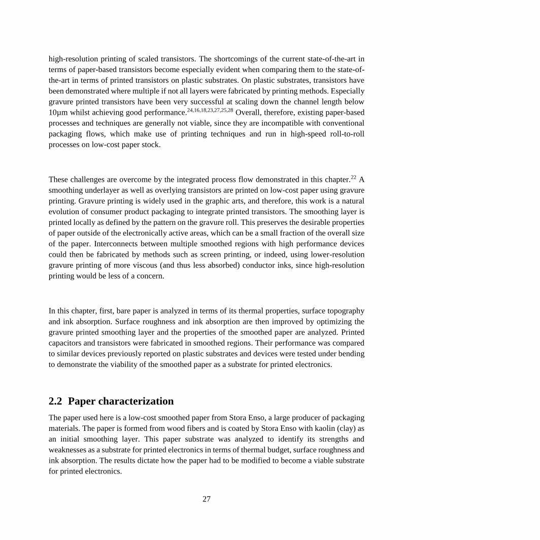
In this chapter, first, bare paper is analyzed in terms of its thermal properties, surface topography
and ink absorption. Surface roughness and ink absorption are then improved by optimizing the
gravure printed smoothing layer and the properties of the smoothed paper are analyzed. Printed
capacitors and transistors were fabricated in smoothed regions. Their performance was compared
to similar devices previously reported on plastic substrates and devices were tested under bending
to demonstrate the viability of the smoothed paper as a substrate for printed electronics.
2.2 Paper characterization
The paper used here is a low-cost smoothed paper from Stora Enso, a large producer of packaging
materials. The paper is formed from wood fibers and is coated by Stora Enso with kaolin (clay) as
an initial smoothing layer. This paper substrate was analyzed to identify its strengths and
weaknesses as a substrate for printed electronics in terms of thermal budget, surface roughness and
ink absorption. The results dictate how the paper had to be modified to become a viable substrate
for printed electronics.

28
The thermal budget is a key property of a substrate because it dictates which processes can be
performed on it. The thermal budget of the paper substrate was characterized qualitatively in terms
of darkening and mechanical degradation (see Figure 2-1) as well as quantitatively by
thermogravimetric analysis (TGA) (see Figure 2-2). Qualitatively, first signs of degradation are
observed at about 250°C and TGA confirms that no significant degradation occurs below 300°C.
This is higher than all low-cost plastics and photo papers, and attests to the viability of the kaolin
coating to produce highly stable paper substrates for printed electronics. It is certainly compatible
with organic electronics and, in the future, might also allow the use of solution processed inorganic
materials with higher temperature requirements.102
Figure 2-1. Qualitative paper degradation with temperature for three different papers:
Precipitated calcium carbonate (PCC) smoothing, Kaolin smoothing and conventional
photo paper. Kaolin-smoothed paper was used throughout this work.
Gets brittle Darkens No ignition
Darkens Gets brittle No ignition
Coating melts
150 200 250 300 350 400 450
T (˚C)
PCC Kaolin Photo paper
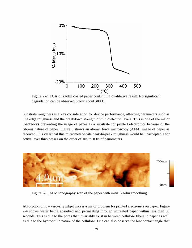
29
Figure 2-2. TGA of kaolin coated paper confirming qualitative result. No significant
degradation can be observed below about 300˚C.
Substrate roughness is a key consideration for device performance, affecting parameters such as
line edge roughness and the breakdown strength of thin dielectric layers. This is one of the major
roadblocks preventing the usage of paper as a substrate for printed electronics because of the
fibrous nature of paper. Figure 3 shows an atomic force microscopy (AFM) image of paper as
received. It is clear that this micrometer-scale peak-to-peak roughness would be unacceptable for
active layer thicknesses on the order of 10s to 100s of nanometers.
Figure 2-3. AFM topography scan of the paper with initial kaolin smoothing.
Absorption of low viscosity inkjet inks is a major problem for printed electronics on paper. Figure
2-4 shows water being absorbed and permeating through untreated paper within less than 30
seconds. This is due to the pores that invariably exist in between cellulose fibers in paper as well
as due to the hydrophilic nature of the cellulose. One can also observe the low contact angle that
755nm
0nm
754.96
0.00

30
the water makes with the paper due to its hydrophilic nature as well as due to uncontrolled lateral
fluid spreading. These issues make it very difficult to print well defined features onto bare paper.
Figure 2-5 shows inkjet printed silver lines on bare paper. The ink has been absorbed and it has
spread laterally leading to irregular features. Silver lines also exhibited poor conductivity after
being absorbed by the paper.
Figure 2-4. Water absorption into bare paper. Within less than 30 seconds the water
droplet has completed permeated through the paper.
Figure 2-5. Inkjet printed silver lines onto bare kaolin paper. Ink has been absorbed by
the paper and shows poor feature definition due to lateral spreading.
4 sec 26 sec 12 sec
100µm
31
2.3 Paper modification
Thus, a method is needed to modify the paper. Surface roughness as well as ink absorption and
spreading need to be reduced significantly. The modification of paper to prevent fluid flow is well
known in the field of paper microfluidics.103 Barriers to fluid flow are created inside of paper to
define channels that fluid can flow through. There are two main techniques to create barriers inside
the paper. One technique prevents fluid flow by hydrophobizing the paper. This can be achieved
by changing the chemical end groups of the paper fibers from the hydrophilic hydroxyl groups of
cellulose to more hydrophobic groups. This was attempted first. However, there are two main
drawbacks that make hydrophobized paper unsuitable for printed electronics. Firstly, it does not
solve the roughness problem. Secondly, printing on top of hydrophobized paper is challenging
because ink will not wet the paper. The second technique used in paper microfluidics is the
physical blocking of the paper pores to prevent fluid flow through them. Often, hydrophobic
materials are used to block pores. Here, we can employ a similar strategy to modify the paper;
however, with a few important differences. Since the goal is to print electronics on top of the
modified paper, only the paper pores on the top side need to be blocked rather than all pores
throughout the paper thickness. In addition to the blocking of paper pores, the final surface
roughness needs to be minimized. The material used to block pores and smooth the surface also
needs to have favorable properties. It needs to exhibit good wetting properties. It needs to exhibit
sufficient solvent resistance and sufficient thermal stability to withstand subsequent processing.
Poly-4-vinylphenol (PVP) was chosen as the smoothing material. PVP can be readily dissolved in
propylene glycol monomethyl ether acetate (PGMEA) for printing. It was cross-linked with poly
melamine-co-formaldehyde methylated at 210°C for added stability. The PVP smoothing material
was analyzed to find its maximum processing temperature. TGA of cross-linked PVP shows that
degradation begins at approximately 210°C (see Figure 2-6). This is sufficient for organic
electronics, but could be improved in the future to fully utilize the thermal capabilities of the paper.

32
Figure 2-6. TGA of cross-linked PVP confirming sufficient thermal stability to allow
organic electronics to be fabricated on top.
The robustness of the PVP to solvent exposure after heat treatment was also tested. A thin layer of
PVP was deposited onto glass slides by spin coating and subsequently cross-linked. The PVP was
heated to different temperatures for 30 minutes and film thickness was measured. Subsequently,
the PVP was exposed to acetone for one minute and the thickness was measured again. Whilst the
thickness decreased after heat treatment, exposure to acetone only attacked the PVP after the PVP
had been exposed to temperatures above 300°C (see Figure 2-7). This further confirms the viability
of the PVP as a substrate for printed electronics.
Figure 2-7. PVP degradation after exposure to high temperatures and after subsequent
solvent exposure. PVP only loses solvent resistance after exposure to temperatures
above 300°C.
0
50
100
150
200
250
300
200 250 300 350
PV
P t
hic
kne
ss (
nm
)
Temperature (°C)
No acetone
1min acetone
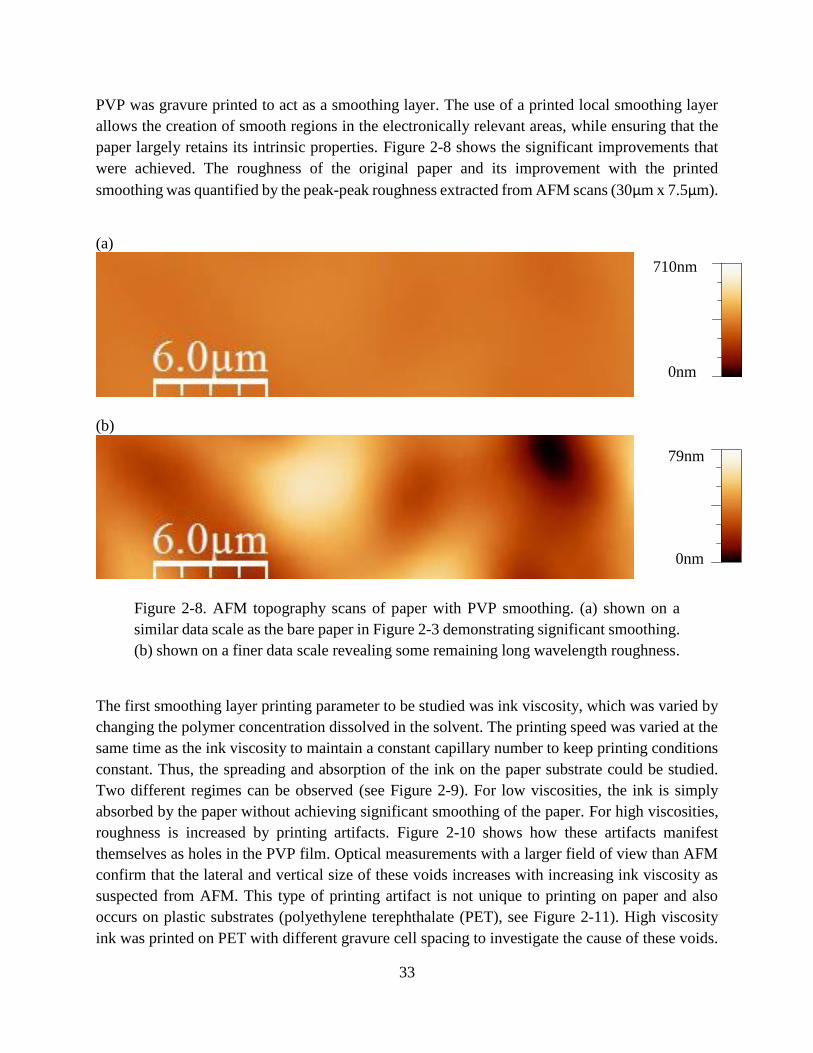
33
PVP was gravure printed to act as a smoothing layer. The use of a printed local smoothing layer
allows the creation of smooth regions in the electronically relevant areas, while ensuring that the
paper largely retains its intrinsic properties. Figure 2-8 shows the significant improvements that
were achieved. The roughness of the original paper and its improvement with the printed
smoothing was quantified by the peak-peak roughness extracted from AFM scans (30µm x 7.5µm).
(a)
(b)
Figure 2-8. AFM topography scans of paper with PVP smoothing. (a) shown on a
similar data scale as the bare paper in Figure 2-3 demonstrating significant smoothing.
(b) shown on a finer data scale revealing some remaining long wavelength roughness.
The first smoothing layer printing parameter to be studied was ink viscosity, which was varied by
changing the polymer concentration dissolved in the solvent. The printing speed was varied at the
same time as the ink viscosity to maintain a constant capillary number to keep printing conditions
constant. Thus, the spreading and absorption of the ink on the paper substrate could be studied.
Two different regimes can be observed (see Figure 2-9). For low viscosities, the ink is simply
absorbed by the paper without achieving significant smoothing of the paper. For high viscosities,
roughness is increased by printing artifacts. Figure 2-10 shows how these artifacts manifest
themselves as holes in the PVP film. Optical measurements with a larger field of view than AFM
confirm that the lateral and vertical size of these voids increases with increasing ink viscosity as
suspected from AFM. This type of printing artifact is not unique to printing on paper and also
occurs on plastic substrates (polyethylene terephthalate (PET), see Figure 2-11). High viscosity
ink was printed on PET with different gravure cell spacing to investigate the cause of these voids.
754.96
0.00
710nm
0nm
754.96
0.00
79nm
0nm

34
The size of voids increases with increasing cell spacing ultimately leading to isolated drops of size
comparable with the cell size (see Figure 2-12). This suggests that voids are not caused by printing
instabilities but rather due to insufficient spreading of high viscosity inks during drying. The
optimum ink viscosity was found to be approximately 150cP.
Figure 2-9. Roughness optimization with PVP viscosity showing optimal smoothing
at intermediate viscosities (5 layers of PVP).
Figure 2-10. Optical micrographs showing absorption of ink for low viscosity ink and
increasingly large printing artifacts with increasing ink viscosity (5 layers of PVP).
80cP 261cP
412cP 718cP

35
Figure 2-11. Optical micrograph of printing artifacts on plastic (PET) confirming that
printing artifacts are independent of paper substrate (7 layers of PVP, 718cP).
Figure 2-12. Optical profilometry images for different cell spacing (CS) with constant
cell size 15µm printed on PET (1 layer of PVP). The increased size of holes in the film
with increasing cell spacing, ultimately leading to isolated drops of the same size as
the cells, confirms that printing artifacts are due to high viscosity inks (here 2500cP)
not being able to flow between cells before drying.
The effect of gravure cell size and the number of PVP layers was investigated using ink with
optimized viscosity. Not surprisingly, roughness decreases with increasing cell size and number
of layers due to the larger volume of ink deposited per unit area (see Figure 2-13). The decrease
with number of layers follows a non-linear trend leading to diminishing returns for large numbers
of layers. This can be understood from cross-sectional images (see Figure 2-14). For one and two
layers of smoothing, one cannot make out a continuous PVP layer because not all pores in the
paper are filled. For three, four and five layers, one can extract a thickness of the PVP layer (see
Figure 2-15). This follows a linear trend. For each additional layer, the already printed PVP, which
CS 1.25μm CS 2.5μm
CS 4μm CS 7.5μm
15μm
15μm
15μm
15μm

36
is not cross-linked yet, is re-dissolved and thus allowed to penetrate the paper further. This explains
why the improvements in smoothing diminish once three layers have been printed. The linear trend
line can be extrapolated to cross the x-axis in between 2 and 3 layers. This suggests that there will
be no continuous PVP layer for fewer than three layers, which is also observed in the cross-
sectional images.
Figure 2-13. Pk-pk roughness with optimized ink viscosity (140cP) showing improved
roughness with increasing cell depth and number of layers. The cells here were larger
than the cells used to obtain the results in Figure 2-9 further confirming the importance
of large cells.
Figure 2-14. Cross-sectional optical micrographs of paper smoothed with an
increasing number of PVP layers. A continuous smoothing layer becomes visible for
3 or more layers.
50µm
5 layers 1 layer
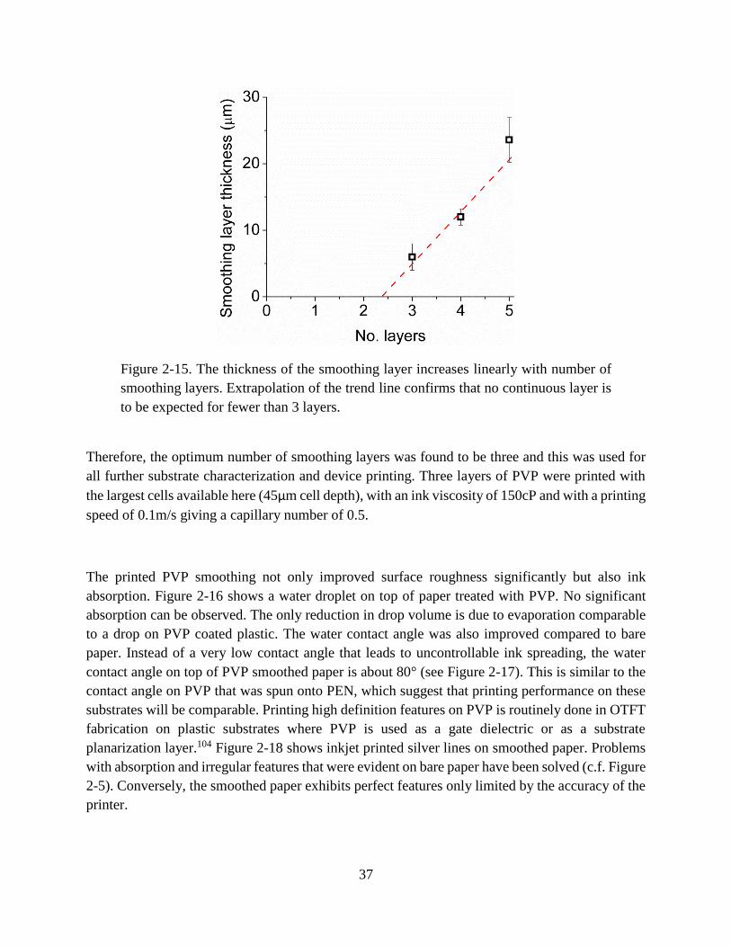
37
Figure 2-15. The thickness of the smoothing layer increases linearly with number of
smoothing layers. Extrapolation of the trend line confirms that no continuous layer is
to be expected for fewer than 3 layers.
Therefore, the optimum number of smoothing layers was found to be three and this was used for
all further substrate characterization and device printing. Three layers of PVP were printed with
the largest cells available here (45µm cell depth), with an ink viscosity of 150cP and with a printing
speed of 0.1m/s giving a capillary number of 0.5.
The printed PVP smoothing not only improved surface roughness significantly but also ink
absorption. Figure 2-16 shows a water droplet on top of paper treated with PVP. No significant
absorption can be observed. The only reduction in drop volume is due to evaporation comparable
to a drop on PVP coated plastic. The water contact angle was also improved compared to bare
paper. Instead of a very low contact angle that leads to uncontrollable ink spreading, the water
contact angle on top of PVP smoothed paper is about 80° (see Figure 2-17). This is similar to the
contact angle on PVP that was spun onto PEN, which suggest that printing performance on these
substrates will be comparable. Printing high definition features on PVP is routinely done in OTFT
fabrication on plastic substrates where PVP is used as a gate dielectric or as a substrate
planarization layer.104 Figure 2-18 shows inkjet printed silver lines on smoothed paper. Problems
with absorption and irregular features that were evident on bare paper have been solved (c.f. Figure
2-5). Conversely, the smoothed paper exhibits perfect features only limited by the accuracy of the
printer.
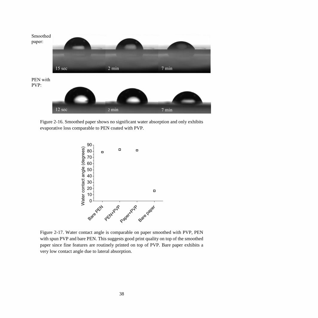
38
Figure 2-16. Smoothed paper shows no significant water absorption and only exhibits
evaporative loss comparable to PEN coated with PVP.
Bare
PEN
PEN+P
VP
Paper
+PVP
Bare
pape
r
0
10
20
30
40
50
60
70
80
90
Wa
ter
co
nta
ct a
ng
le (
de
gre
es)
Figure 2-17. Water contact angle is comparable on paper smoothed with PVP, PEN
with spun PVP and bare PEN. This suggests good print quality on top of the smoothed
paper since fine features are routinely printed on top of PVP. Bare paper exhibits a
very low contact angle due to lateral absorption.
2 min
12 sec
15 sec 7 min
2 min 7 min
PEN with
PVP:
Smoothed
paper:
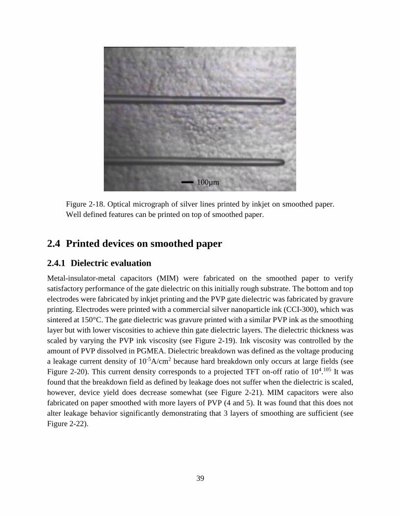
39
Figure 2-18. Optical micrograph of silver lines printed by inkjet on smoothed paper.
Well defined features can be printed on top of smoothed paper.
2.4 Printed devices on smoothed paper
2.4.1 Dielectric evaluation
Metal-insulator-metal capacitors (MIM) were fabricated on the smoothed paper to verify
satisfactory performance of the gate dielectric on this initially rough substrate. The bottom and top
electrodes were fabricated by inkjet printing and the PVP gate dielectric was fabricated by gravure
printing. Electrodes were printed with a commercial silver nanoparticle ink (CCI-300), which was
sintered at 150°C. The gate dielectric was gravure printed with a similar PVP ink as the smoothing
layer but with lower viscosities to achieve thin gate dielectric layers. The dielectric thickness was
scaled by varying the PVP ink viscosity (see Figure 2-19). Ink viscosity was controlled by the
amount of PVP dissolved in PGMEA. Dielectric breakdown was defined as the voltage producing
a leakage current density of 10-5A/cm2 because hard breakdown only occurs at large fields (see
Figure 2-20). This current density corresponds to a projected TFT on-off ratio of 104.105 It was
found that the breakdown field as defined by leakage does not suffer when the dielectric is scaled,
however, device yield does decrease somewhat (see Figure 2-21). MIM capacitors were also
fabricated on paper smoothed with more layers of PVP (4 and 5). It was found that this does not
alter leakage behavior significantly demonstrating that 3 layers of smoothing are sufficient (see
Figure 2-22).
100µm
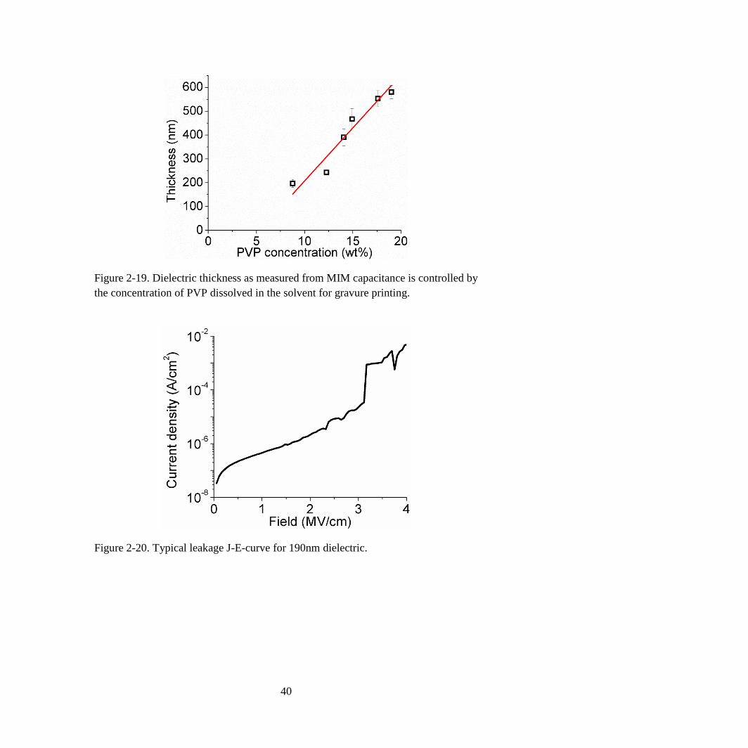
40
Figure 2-19. Dielectric thickness as measured from MIM capacitance is controlled by
the concentration of PVP dissolved in the solvent for gravure printing.
Figure 2-20. Typical leakage J-E-curve for 190nm dielectric.
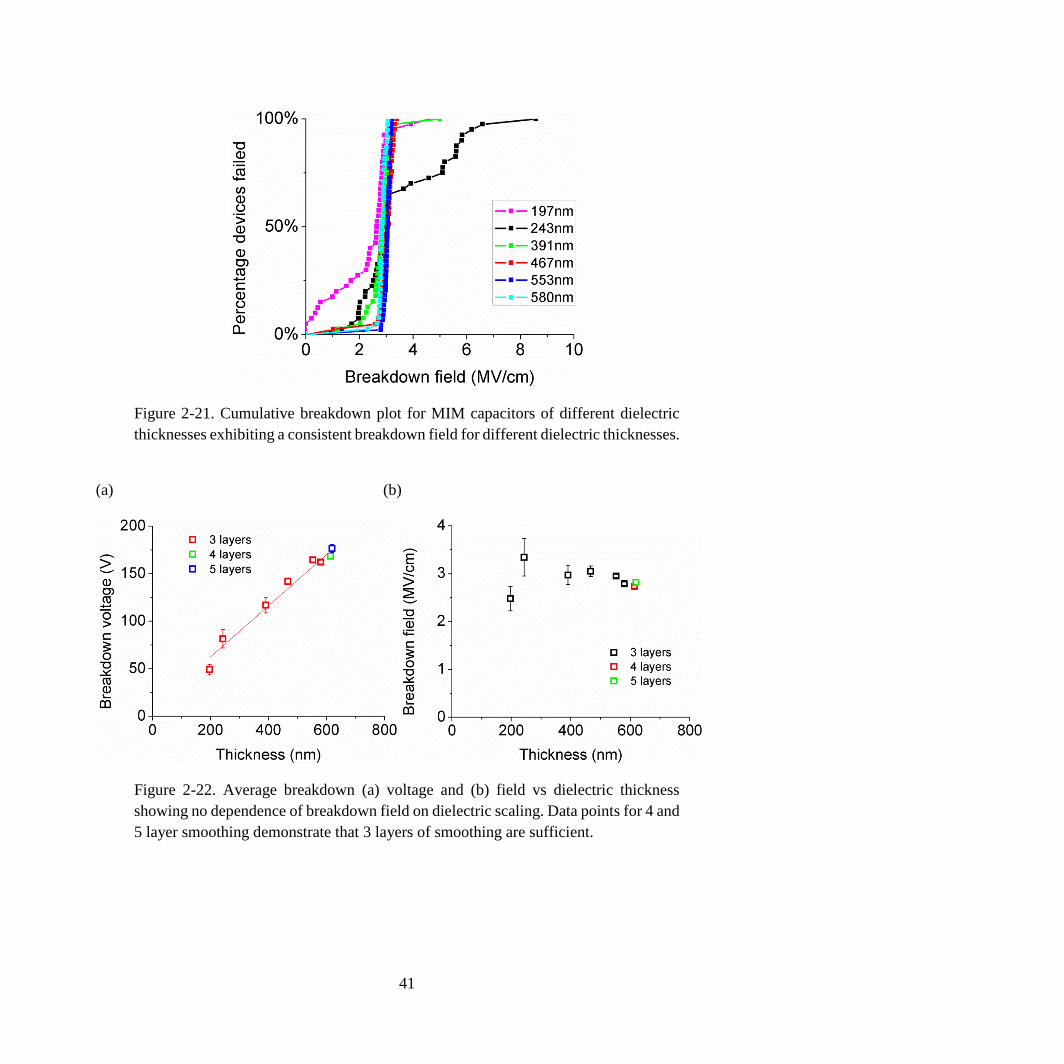
41
Figure 2-21. Cumulative breakdown plot for MIM capacitors of different dielectric
thicknesses exhibiting a consistent breakdown field for different dielectric thicknesses.
(a) (b)
Figure 2-22. Average breakdown (a) voltage and (b) field vs dielectric thickness
showing no dependence of breakdown field on dielectric scaling. Data points for 4 and
5 layer smoothing demonstrate that 3 layers of smoothing are sufficient.

42
2.4.2 Printed transistors on paper
Organic TFTs were fabricated with the same process as for the thinnest gate dielectric. Bottom-
gate, bottom-contact OTFTs were fabricated using a spun poly(2,5-bis (3-tetradecyl-thiophen-2-
yl)thieno[3,2-b]thiophene) (pBTTT) semiconductor layer on top. Spin coating was chosen because
it could be performed under an inert nitrogen atmosphere. However, OTFTs with printed pBTTT
have been demonstrated in the past86 making this a fully printable process flow. All transistor
measurements were conducted under a nitrogen atmosphere. The TFT fabrication process flow is
illustrated in Figure 2-23. Figure 2-24 shows an optical micrograph of printed transistors on locally
smoothed pads demonstrating both high quality printed features as well as the truly local nature of
smoothed pads.
Figure 2-23. Schematic illustration of TFT process flow. The process flow is identical
for MIM capacitors except that the last semiconductor deposition step is omitted and
the electrodes are fully overlapped. (i) Rough paper with initial Kaolin smoothing. (ii)
Gravure print local smoothing poly-4-vinylphenol (PVP), cross-link 210˚C 30
minutes. (iii) Inkjet print bottom gate silver (CCI-300), sinter 150˚C 30 minutes. (iv)
Gravure print PVP gate dielectric, cross-link 210˚C 30 minutes. (v) Inkjet print source
and drain silver (CCI-300), sinter 150˚C 30 minutes. (vi) UVO 10 minutes, Spin coat
pBTTT C16, Anneal 160˚C 10 minutes, cool slowly.
(i) (ii) (iii)
(iv) (v) (vi)

43
Figure 2-24. Optical micrograph of fully printed transistors on locally printed PVP
smoothing (bright pads). The unmodified paper is visible as the dark areas surrounding
smoothed pads.
The transistor performance was optimized106 by exposing the source/ drain and gate dielectric to
10 minutes of UV ozone treatment before semiconductor deposition. When the sample was not
treated with UVO before semiconductor deposition, mobility was found to be significantly lower,
especially in the linear regime by about three orders of magnitude (see Figure 2-25). One can
compare the IdVd-characteristics of two devices with and without UVO treatment (see Figure
2-26). Untreated devices show a clear non-linearity in the non-saturation regime suggesting a
significant contact barrier. This explains why the difference is more significant for the linear
mobility than the saturation mobility. The removal of the contact barrier might be due to a slight
oxidation of the silver electrodes under UVO treatment. The work function of pristine silver at
4.3eV is not well matched to the HOMO level of pBTTT at 5.1eV.107 Oxidation of the silver can
increase its work function by 0.7eV resulting in much improved injection.108 The UVO treatment
might also improve injection by removing organic residue left on the surface after sintering of the
printed silver nanoparticles.
200μm
Rough paper with initial
Kaolin smoothing
Local PVP smoothing
TFT

44
(a) (b)
Figure 2-25. Comparison of electrical performance for different processing conditions:
(i) slow cooling after pBTTT annealing and prior UVO treatment of electrodes, (ii)
fast cooling after pBTTT annealing and UVO treatment and (iii) slow cooling after
pBTTT annealing and no UVO treatment.
(a) (b)
Figure 2-26. IdVd-characteristics of OTFT a) with and b) without UVO treatment.
One can clearly observe the differences in non-linearity in the unsaturated regime
indicating a contact barrier without UVO treatment.
The pBTTT was annealed at 160°C after spin coating. This temperature was chosen to lie above
the transition temperature to the liquid-crystalline phase.107,109 The film crystallizes into its final
microstructure upon cooling. Two different cooling rates were explored to improve device
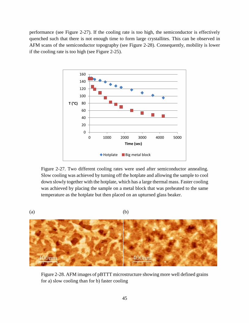
45
performance (see Figure 2-27). If the cooling rate is too high, the semiconductor is effectively
quenched such that there is not enough time to form large crystallites. This can be observed in
AFM scans of the semiconductor topography (see Figure 2-28). Consequently, mobility is lower
if the cooling rate is too high (see Figure 2-25).
Figure 2-27. Two different cooling rates were used after semiconductor annealing.
Slow cooling was achieved by turning off the hotplate and allowing the sample to cool
down slowly together with the hotplate, which has a large thermal mass. Faster cooling
was achieved by placing the sample on a metal block that was preheated to the same
temperature as the hotplate but then placed on an upturned glass beaker.
(a) (b)
Figure 2-28. AFM images of pBTTT microstructure showing more well defined grains
for a) slow cooling than for b) faster cooling
0
20
40
60
80
100
120
140
160
0 1000 2000 3000 4000 5000
T (°C)
Time (sec)
Hotplate Big metal block
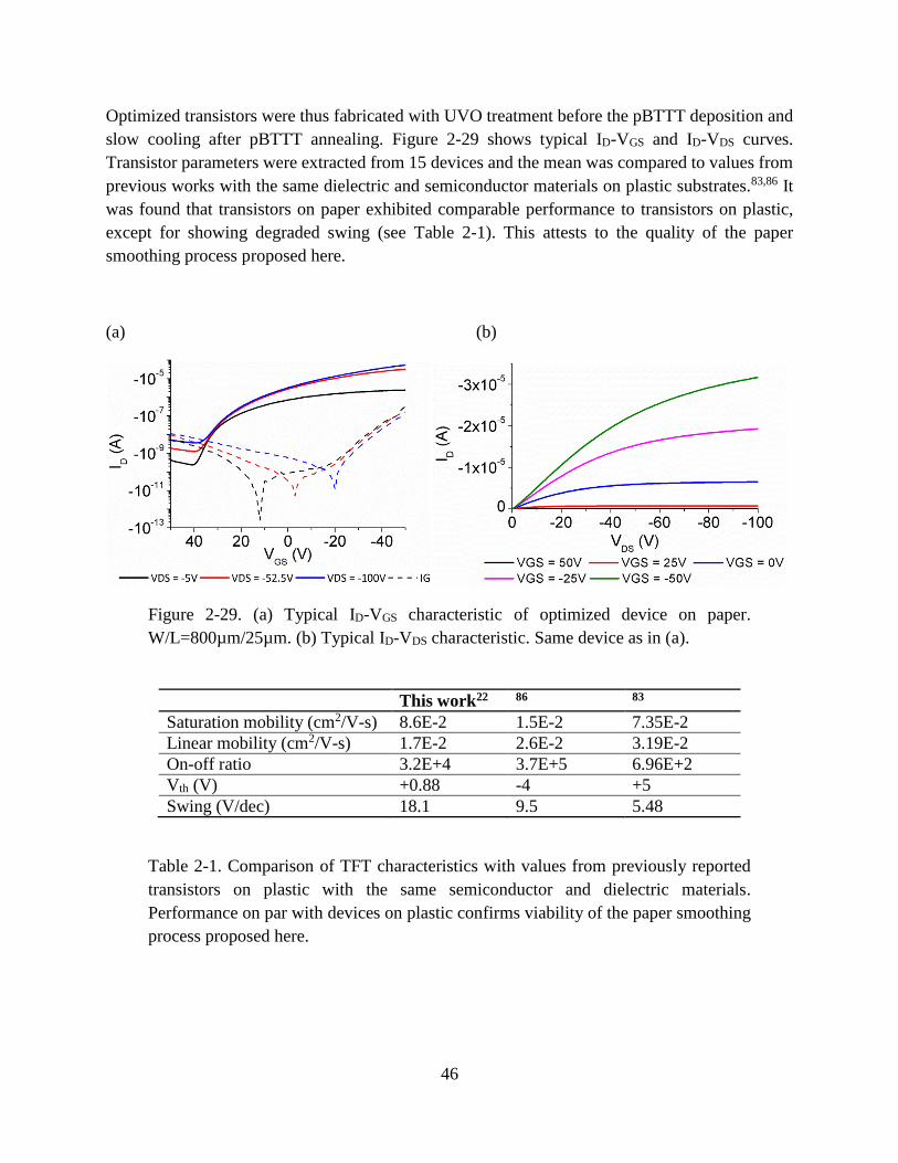
46
Optimized transistors were thus fabricated with UVO treatment before the pBTTT deposition and
slow cooling after pBTTT annealing. Figure 2-29 shows typical ID-VGS and ID-VDS curves.
Transistor parameters were extracted from 15 devices and the mean was compared to values from
previous works with the same dielectric and semiconductor materials on plastic substrates.83,86 It
was found that transistors on paper exhibited comparable performance to transistors on plastic,
except for showing degraded swing (see Table 2-1). This attests to the quality of the paper
smoothing process proposed here.
(a) (b)
Figure 2-29. (a) Typical ID-VGS characteristic of optimized device on paper.
W/L=800µm/25µm. (b) Typical ID-VDS characteristic. Same device as in (a).
This work22 86 83
Saturation mobility (cm2/V-s) 8.6E-2 1.5E-2 7.35E-2
Linear mobility (cm2/V-s) 1.7E-2 2.6E-2 3.19E-2
On-off ratio 3.2E+4 3.7E+5 6.96E+2
Vth (V) +0.88 -4 +5
Swing (V/dec) 18.1 9.5 5.48
Table 2-1. Comparison of TFT characteristics with values from previously reported
transistors on plastic with the same semiconductor and dielectric materials.
Performance on par with devices on plastic confirms viability of the paper smoothing
process proposed here.

47
2.4.3 Bending tests
Most applications for printed systems on paper will require flexible and bendable electronics. The
mechanical robustness of the devices fabricated here was thus investigated under bending. A series
of cylindrical dowels was used to define controlled bending radii. A PEN carrier was used to
facilitate handling. This leads to a larger strain in the devices compared to just bending the paper
to the same radius. The Young’s moduli of both paper and PEN were measured. Treating the
sandwich as a composite beam with no uniaxial tension or compression, the strain in the devices
and an equivalent bending radius for just bending the paper without a carrier were calculated (see
Appendix A for further details).
TFTs on paper were strained in the direction parallel to current flow. No significant device
degradation within the measurement error and device-to-device variation could be observed up to
a strain of 2.2% (equivalent bending radius 1.59mm). The paper itself tore when bent to the next
smaller radius. Figure 2-30 shows the evolution of saturation mobility under bending, which
reveals no significant degradation upon bending. Other parameters showed similar behavior. This
confirms that this device structure is robust against bending up to the failure point of the paper.
Figure 2-30. Saturation mobility box plots under bending and unbent before and after
bending showing no significant degradation under bending. Conditions are plotted in
the same order that the experiment was conducted in. Here samples were treated with
only 5 minutes of UVO instead of 10 minutes leading to slightly lowered mobility.

48
Under stress in the direction perpendicular to current flow, the most likely failure mechanism
would be cracking of the electrodes. The sheet resistance of the printed silver lines was measured
as a function of bending and again no significant degradation could be observed (see Figure 2-31).
These results attest to the robustness of printed electronics on paper under bent conditions.
Figure 2-31. Sheet resistance of silver lines under bending confirming robustness to
bending.
2.5 Conclusions
This chapter demonstrates that roll-to-roll printing can overcome major roadblocks towards printed
electronics on paper. A locally printed smoothing underlayer was shown to tremendously improve
surface roughness, ink absorption and printability. Printed transistors were fabricated on low-cost
paper using this technique, and were shown to exhibit performance comparable to similar
transistors on a plastic substrate that had been reported previously. Robustness of devices to
bending was also demonstrated. This thus represents an important step towards the realization of
smart consumer packaging integrating printed circuits directly onto packaging stock.
49
The focus of this chapter was the smoothing of paper using gravure printing. Transistors were
fabricated with established materials and printing methods to demonstrate the viability of the
smoothed paper as a substrate. The following chapters will focus on pushing the performance of
the device printing itself, which requires scaling of both lateral and thickness dimensions. The next
chapter will thus discuss a new gravure roll fabrication technology that enables the lateral
downscaling of feature sizes whilst achieving high printing throughput.
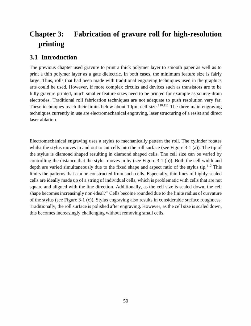
50
Chapter 3: Fabrication of gravure roll for high-resolution
printing
3.1 Introduction
The previous chapter used gravure to print a thick polymer layer to smooth paper as well as to
print a thin polymer layer as a gate dielectric. In both cases, the minimum feature size is fairly
large. Thus, rolls that had been made with traditional engraving techniques used in the graphics
arts could be used. However, if more complex circuits and devices such as transistors are to be
fully gravure printed, much smaller feature sizes need to be printed for example as source-drain
electrodes. Traditional roll fabrication techniques are not adequate to push resolution very far.
These techniques reach their limits below about 10µm cell size.110,111 The three main engraving
techniques currently in use are electromechanical engraving, laser structuring of a resist and direct
laser ablation.
Electromechanical engraving uses a stylus to mechanically pattern the roll. The cylinder rotates
whilst the stylus moves in and out to cut cells into the roll surface (see Figure 3-1 (a)). The tip of
the stylus is diamond shaped resulting in diamond shaped cells. The cell size can be varied by
controlling the distance that the stylus moves in by (see Figure 3-1 (b)). Both the cell width and
depth are varied simultaneously due to the fixed shape and aspect ratio of the stylus tip.112 This
limits the patterns that can be constructed from such cells. Especially, thin lines of highly-scaled
cells are ideally made up of a string of individual cells, which is problematic with cells that are not
square and aligned with the line direction. Additionally, as the cell size is scaled down, the cell
shape becomes increasingly non-ideal.23 Cells become rounded due to the finite radius of curvature
of the stylus (see Figure 3-1 (c)). Stylus engraving also results in considerable surface roughness.
Traditionally, the roll surface is polished after engraving. However, as the cell size is scaled down,
this becomes increasingly challenging without removing small cells.
51
(a) (b) (c)
Figure 3-1. (a) Electromechanical engraving operates by cutting material from the
rotating roll with a stylus that moves in and out according to the cell pattern. Reprinted
with permission from 83. (b) Cells are diamond shaped. Traditionally the color tone of
a cell array is varied by varying the cell size and density. Reprinted with permission
from 110. (c) As cells are scaled down, the cell shape becomes increasing non-ideal and
rounded. One can also observe scratches in the roll surface from the engraving process.
Reprinted from 23 with permission from Elsevier.
The other two engraving technologies that are commonly used rely on laser patterning. A laser
beam is used to either pattern the roll directly by ablation (see Figure 3-2) or to pattern a
photoactive resist that is used as a mask during chemical etching of the cells. Both methods are
limited by the spot size of the laser beam on the roll surface. Focusing is a challenge on the curved
roll surface that is rotating, especially if the concentricity of the cylinder is not ideal. A round laser
beam will result in round cells which is again not ideal for highly-scaled lines. Chemical etching
of features is further limited by the isotropic nature of the etch resulting in undercutting of the
resist thus increasing minimum feature size. Direct ablation of material requires much higher laser
powers. Ideally, the metal is directly evaporated without leaving any residue. In reality, it is very
difficult to create perfect cell shapes without any burrs. The size of burrs has been reduced to 2-
3µm by using electroplated zinc with organic additives instead of copper that is traditionally used
to fabricate rolls.110 However, this size of burr is still large if cells are scaled below 5µm.

52
(a) (b)
Figure 3-2. (a) Direct laser engraving uses a high-power laser to ablate metal from the
roll. (b) 3D profiles showing cell shapes after laser engraving. Both panels reprinted
with permission from 110.
These limitations of traditional engraving techniques mean that a novel method of fabricating
gravure rolls is required to successfully push resolution below 5µm. Silicon printing plates offer a
route towards this goal. They can be fabricated using traditional microfabrication techniques
including photolithography and dry and wet etching. Superior control over cell size, cell shape and
surface roughness can be achieved in comparison to traditional roll fabrication techniques. Indeed,
some of the best reported results in terms of printing high-resolution features at high print speeds
have been obtained using silicon printing plates.28,49,27,113 However, the main drawback of silicon
printing plates is their form factor. For lab-scale experiments, a plastic substrate is wrapped around
a rubber cylinder and rolled over such a flat silicon printing plate. However, this is not possible
for continuous high-speed printing to achieve low-cost manufacturing with a mass-production roll-
to-roll or sheet-fed printer. The superior properties of the silicon printing plate thus need to be
transferred to the form factor of a roll. One way to do so is to thin the silicon plate down sufficiently
such that it becomes flexible enough to be wrapped around a roller. However, there are concerns
whether such a silicon plate would withstand the stresses of printing both in terms of nip pressure
and doctor blade pressure without cracking. Indeed, the first demonstration of this method does
not use a doctor blade limiting the print speed to 10mm/sec.114 This chapter describes a different
approach where a flexible metal plate is created that has the same surface topology as the silicon
printing plate. This metal plate is wrapped around a cylinder to be used as a roll for gravure

53
printing. With this novel gravure roll, a printing resolution down to 2µm linewidths can be
achieved.115
In this chapter, the novel roll fabrication process and its optimization are described first. Printing
with such rolls is analyzed next. Mounting of the plate on a magnetic roller is discussed. Two
different surface modifications are contrasted and it is shown how they affect printing performance
as well as wear during extended print runs.
3.2 Roll fabrication process
The first step in the roll fabrication process is the fabrication of the silicon master.
Photolithography is used to define the cell features with a critical dimension of 250nm for the
smallest cell gaps. The cells are then etched into the silicon using a silicon dioxide hard mask.
Different cell shapes can be obtained by using different etching methods. Square cells are obtained
using dry etching. Inverted pyramid shapes that resemble the shape obtained from stylus engraving
can be obtained using KOH as the wet etchant for silicon. This limits the orientation of the cells to
be aligned with the 110 crystal plane of the silicon wafer; however, this is not a significant
limitation for most Manhattan style circuit layouts. The details of this process were published
elsewhere.49
In order to fabricate the metal printing plate (see Figure 3-3 for an overview of the process), the
pattern is first transferred from the silicon master into a polymer through a molding step. After
release of the polymer from the silicon mold, the polymer is metallized. First, a chrome gold seed
layer is evaporated. Then, a hard surface layer of nickel with boron nitride particles is applied by
electroless plating.116,117 The electroless plating solution was purchased from Caswell Inc. On top
of this, the main thickness of the printing plate is built up using electroplating of permalloy (80%
nickel, 20% iron).118 By applying the hard layer on top of the polymer molding before the
deposition of the permalloy rather than depositing it on top of the permalloy after release from the
molding, it does not distort the highly-scaled features. Before release of the metal stack from the
polymer molding, the backside of the metal is polished and the metal is diced into the shape of a
rectangular printing plate. The high magnetic permeability of the permalloy allows mounting of
the printing plate on a magnetic roll ready for printing (see Figure 3-4). After release, the metal
surface with the hard layer is a perfect replica of the silicon master (see Figure 3-5 and Figure 3-6).

54
Figure 3-3. Metal plate fabrication process starting from silicon master plate.
Figure 3-4. Final metal plate after polishing, dicing and lift-off from PUA mold ready
to be wrapped around magnetic cylinder for printing.
Figure 3-5. Optical micrographs of printing plate surface after release showing good
feature replication over large areas.
5µm cells
2µm cells
1µm cells
10µm cells
7.5µm cells
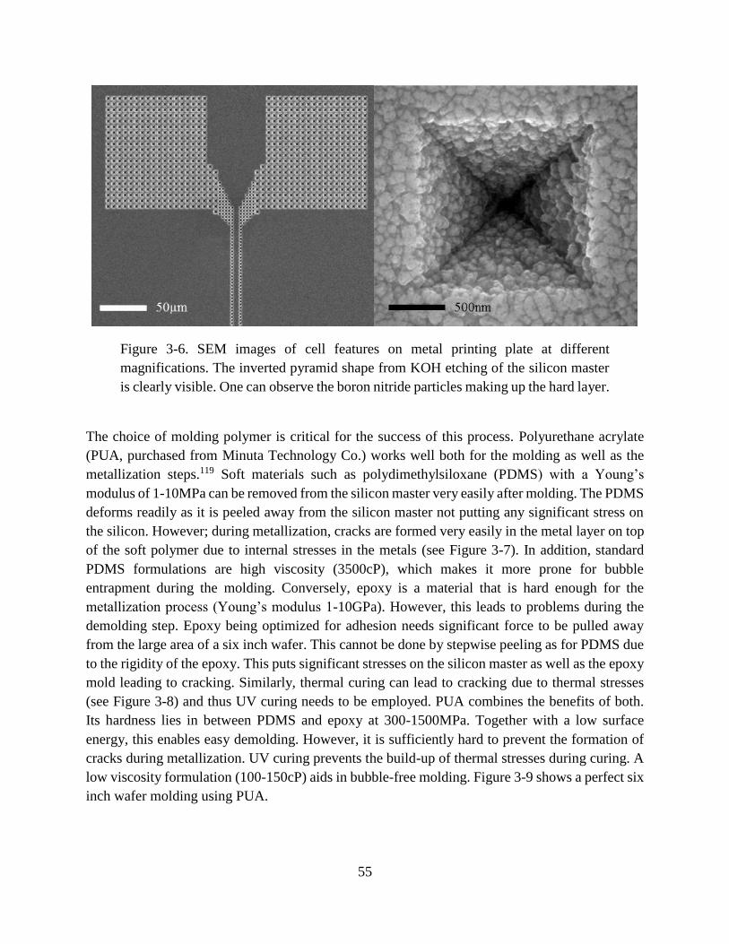
55
Figure 3-6. SEM images of cell features on metal printing plate at different
magnifications. The inverted pyramid shape from KOH etching of the silicon master
is clearly visible. One can observe the boron nitride particles making up the hard layer.
The choice of molding polymer is critical for the success of this process. Polyurethane acrylate
(PUA, purchased from Minuta Technology Co.) works well both for the molding as well as the
metallization steps.119 Soft materials such as polydimethylsiloxane (PDMS) with a Young’s
modulus of 1-10MPa can be removed from the silicon master very easily after molding. The PDMS
deforms readily as it is peeled away from the silicon master not putting any significant stress on
the silicon. However; during metallization, cracks are formed very easily in the metal layer on top
of the soft polymer due to internal stresses in the metals (see Figure 3-7). In addition, standard
PDMS formulations are high viscosity (3500cP), which makes it more prone for bubble
entrapment during the molding. Conversely, epoxy is a material that is hard enough for the
metallization process (Young’s modulus 1-10GPa). However, this leads to problems during the
demolding step. Epoxy being optimized for adhesion needs significant force to be pulled away
from the large area of a six inch wafer. This cannot be done by stepwise peeling as for PDMS due
to the rigidity of the epoxy. This puts significant stresses on the silicon master as well as the epoxy
mold leading to cracking. Similarly, thermal curing can lead to cracking due to thermal stresses
(see Figure 3-8) and thus UV curing needs to be employed. PUA combines the benefits of both.
Its hardness lies in between PDMS and epoxy at 300-1500MPa. Together with a low surface
energy, this enables easy demolding. However, it is sufficiently hard to prevent the formation of
cracks during metallization. UV curing prevents the build-up of thermal stresses during curing. A
low viscosity formulation (100-150cP) aids in bubble-free molding. Figure 3-9 shows a perfect six
inch wafer molding using PUA.
500nm

56
Figure 3-7. Optical micrograph of evaporated chrome-gold on PDMS exhibiting
extensive cracking.
Figure 3-8. Epoxy molding on top of six inch glass carrier wafer that has cracked due
to thermal stresses during curing.
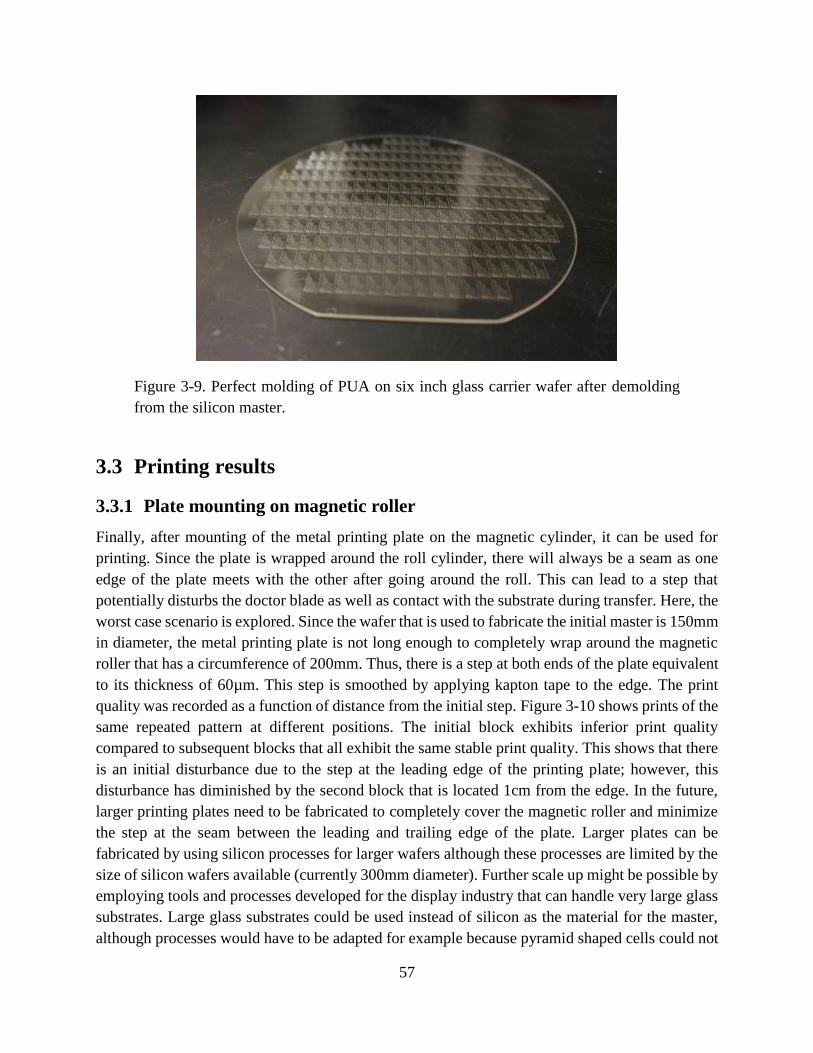
57
Figure 3-9. Perfect molding of PUA on six inch glass carrier wafer after demolding
from the silicon master.
3.3 Printing results
3.3.1 Plate mounting on magnetic roller
Finally, after mounting of the metal printing plate on the magnetic cylinder, it can be used for
printing. Since the plate is wrapped around the roll cylinder, there will always be a seam as one
edge of the plate meets with the other after going around the roll. This can lead to a step that
potentially disturbs the doctor blade as well as contact with the substrate during transfer. Here, the
worst case scenario is explored. Since the wafer that is used to fabricate the initial master is 150mm
in diameter, the metal printing plate is not long enough to completely wrap around the magnetic
roller that has a circumference of 200mm. Thus, there is a step at both ends of the plate equivalent
to its thickness of 60µm. This step is smoothed by applying kapton tape to the edge. The print
quality was recorded as a function of distance from the initial step. Figure 3-10 shows prints of the
same repeated pattern at different positions. The initial block exhibits inferior print quality
compared to subsequent blocks that all exhibit the same stable print quality. This shows that there
is an initial disturbance due to the step at the leading edge of the printing plate; however, this
disturbance has diminished by the second block that is located 1cm from the edge. In the future,
larger printing plates need to be fabricated to completely cover the magnetic roller and minimize
the step at the seam between the leading and trailing edge of the plate. Larger plates can be
fabricated by using silicon processes for larger wafers although these processes are limited by the
size of silicon wafers available (currently 300mm diameter). Further scale up might be possible by
employing tools and processes developed for the display industry that can handle very large glass
substrates. Large glass substrates could be used instead of silicon as the material for the master,
although processes would have to be adapted for example because pyramid shaped cells could not

58
be fabricated by KOH etching anymore. The limited resolution of the lithography used for display
applications compared with nanometer scale silicon lithography is no concern here because the
smallest cells that can efficiently be used for gravure printing are currently larger than 1µm in
width.
Figure 3-10. Optical micrographs of prints at different positions on the roll along the
print direction. The first block of patterns is closest to the leading edge of the plate
mounted on the roll and exhibits the poorest print quality. Print quality stabilizes after
one block. The distance between blocks is 1cm. The large wedge-like shape in block
4 is due to an air bubble that had been entrapped during the PUA molding causing the
doctor blade to momentarily loose contact with the roll surface. Bubbles can be
prevented during the molding process by careful degassing.

59
3.3.2 Printing optimization
In order to achieve optimal printing results and fully utilize the high resolution features on the roll,
the fluid mechanics of the process needs to be optimized. One needs to consider ink properties,
printing speed, doctor blade properties, substrate wetting and roll wetting properties. Optimization
of the wetting properties of the roll surface is enabled by the roll fabrication process proposed here.
The hard layer on top of the main body of the plate can be modified to engineer the roll’s surface
properties. Here, two different surfaces are explored: the bare nickel iron printing plate body and
a boron nitride hard layer. The capillary number was varied to optimize print quality. The ink used
here was again poly-4-vinyl phenol (PVP) dissolved in propylene glycol monomethyl ether acetate
(PGMEA) as a model ink.
3.3.2.1 Printing optimization without hard layer
First, consider printing with a roll where no boron nitride hard layer was deposited. By leaving out
the hard layer, the top surface of the roll is simply the nickel iron that makes up the body of the
plate. One can observe improved print quality for initial increases in printing speed and capillary
number from 1.1 to 2.1 due to the suppression of drag-out (see Figure 3-11). As the doctor blade
passes over the cells, it picks out ink from the cells. This leads to a reduction in ink volume in the
printed feature. At higher values of Ca there is less time for ink to wick up the doctor blade thus
reducing the detrimental effects of drag-out. However, at Ca=4.2, one can also observe breaks in
lines and holes in pads. In this case, the printed ink volume is limited by the cell filling process.
The ink requires time to fully fill the cells due to capillary forces. If Ca is too large, there is not
enough time for this process to complete fully and air is entrapped in the cells.59 Thus optimum
printing without the boron nitride hard layer is achieved at an intermediate capillary number of
2.1. The three parameters that determine Ca are print speed, ink viscosity and ink surface tension.
Assuming surface tension is fixed by the chosen solvent and solute, Ca is proportional to the
product of speed and viscosity. For highly-scaled lines, ink viscosity cannot be changed freely due
to ink spreading on the substrate after transfer. If ink viscosity is too low, ink will spread too far
reducing pattern fidelity. If ink viscosity is too high, ink will not spread sufficiently before drying
to fill in gaps between gravure cells leading to line edge roughness and in the worst case
disconnected lines. Thus, the ideal ink viscosity is small enough to ensure sufficient spreading but
no lower to prevent excessive spreading (see Figure 3-12). This will be studied further in the next
chapter. For an ink viscosity of 110cP, an ideal capillary number of 2 and the surface tension of
PGMEA of 26.9mN/m, this results in an optimum print speed of 0.5m/s. Ideally, one would want
to print at a higher speed to increase fabrication throughput. This can be achieved when the boron
nitride hard layer is employed.

60
Figure 3-11. Optical micrographs of printed features without hard layer. (a) Ca=1.1:
Some holes in print due to drag-out. (b) Ca=2.1: Optimal printing at the cross-over
point between the filling and drag-out limited regimes. (c) Ca=4.2: Significant gaps in
lines due to insufficient filling of cells.
Figure 3-12. Optical micrographs of printed features with different viscosities. (a)
87cP, (b) 113cP, (c) 146cP. The largest viscosity of 146cP leads to some holes in pads
and lines due to insufficient ink spreading on the substrate. The intermediate viscosity
of 113cP leads to complete features. Further reduction of the viscosity leads to further
ink spreading increasing linewidth. Printed with boron nitride hard layer.
3.3.2.2 Printing optimization with hard layer
The addition of the boron nitride layer not only increases the hardness of the roll surface but also
changes its wetting characteristics and thus printing needs to be optimized differently. One can
observe a clear improvement in print quality as Ca is varied over more than one order of magnitude
for a 146cP PVP ink (see Figure 3-13). At Ca=0.11 hardly any ink is printed onto the substrate.
This improves substantially when Ca is increased to 1.1; however, one can still observe holes in
printed rectangles as well as breaks in high resolution lines. These defects are removed when
printing at Ca=5.4. The reason for this significant difference in print quality as Ca is increased is
the reduction of drag-out. In the case of severe drag-out at Ca=0.11 one can also observe

61
characteristic tails of dragged-out ink being re-deposited behind pads. Ca could not be increased
further at this viscosity due to equipment limitations in terms of print speed. Large scale roll-to-
roll gravure printers can print at higher print speeds that might lead to further improvements in
print quality. However, even without being able to probe higher print speeds with the lab-scale
printer used here, the hard layer enables printing at higher speeds than the bare nickel-iron printing
plate.
This difference can be explained by the different wetting properties of the two surfaces. Boron
nitride is used as an extremely slick, low-friction, high lubricity surface coating. This manifests
itself in a smaller contact angle hysteresis (Nickel iron: θR=25°, θA=90°. Boron nitride: θR=40°,
θA=80°.), which enhances both cell filling and drag-out. Cell filling is enhanced by the lower
advancing contact angle, which promotes the advancing of the ink meniscus into the cell during
filling. Similarly, ink can be pulled out from the cell more easily due to the larger receding contact
angle. Thus, the transition from the drag-out limited regime to the filling limited regime is shifted
to higher capillary numbers for the roll with the boron nitride hard layer. For the same viscosity,
this translates into higher printing speeds. This is an economic advantage in the manufacturing of
printed electronics systems since throughput is increased by higher print speeds. With these
optimized printing conditions, the roll with the hard layer can be used to print 2µm lines at a high
speed of 1m/s as can be observed in Figure 3-14.
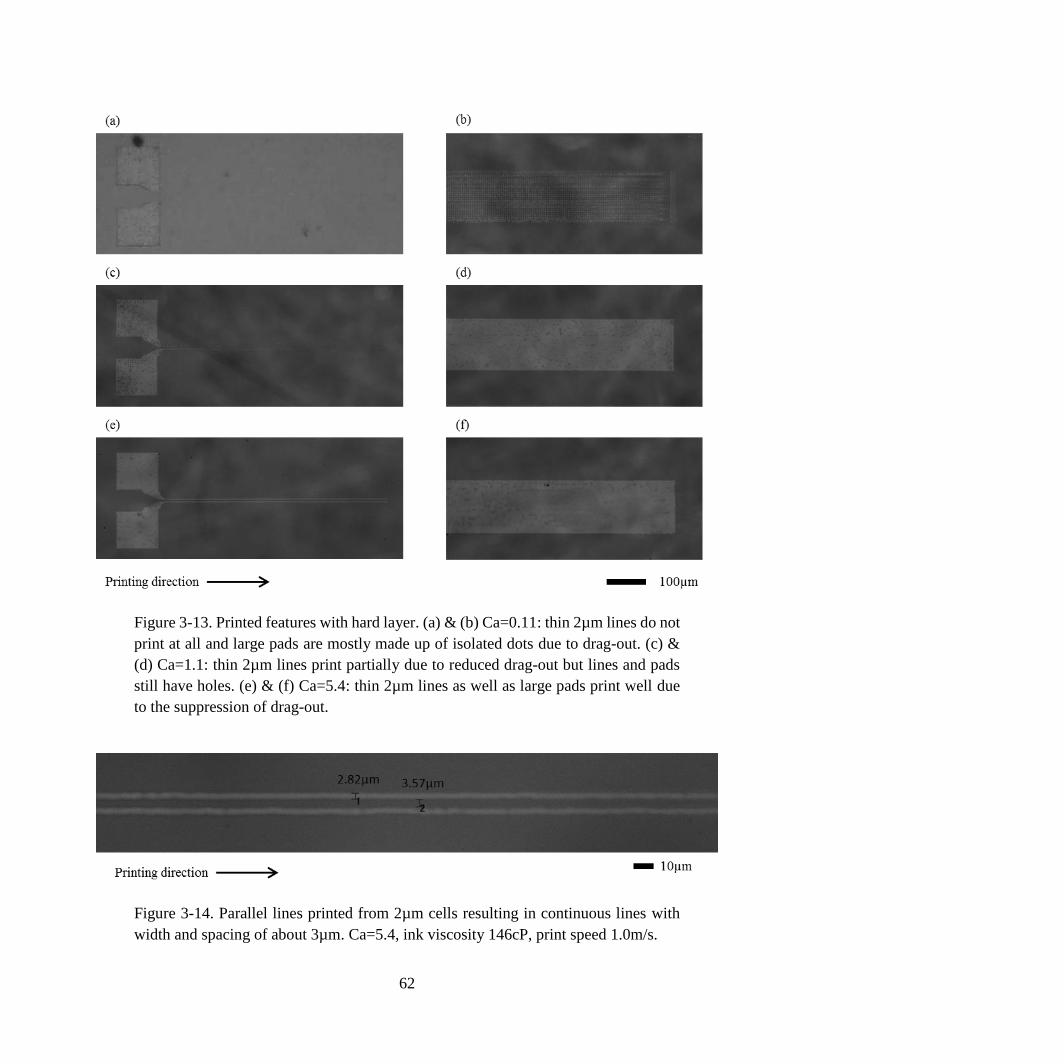
62
Figure 3-13. Printed features with hard layer. (a) & (b) Ca=0.11: thin 2µm lines do not
print at all and large pads are mostly made up of isolated dots due to drag-out. (c) &
(d) Ca=1.1: thin 2µm lines print partially due to reduced drag-out but lines and pads
still have holes. (e) & (f) Ca=5.4: thin 2µm lines as well as large pads print well due
to the suppression of drag-out.
Figure 3-14. Parallel lines printed from 2µm cells resulting in continuous lines with
width and spacing of about 3µm. Ca=5.4, ink viscosity 146cP, print speed 1.0m/s.
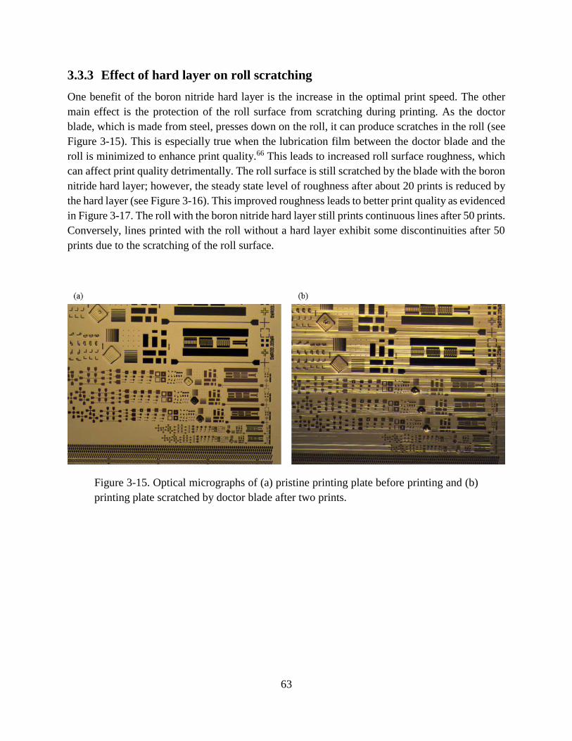
63
3.3.3 Effect of hard layer on roll scratching
One benefit of the boron nitride hard layer is the increase in the optimal print speed. The other
main effect is the protection of the roll surface from scratching during printing. As the doctor
blade, which is made from steel, presses down on the roll, it can produce scratches in the roll (see
Figure 3-15). This is especially true when the lubrication film between the doctor blade and the
roll is minimized to enhance print quality.66 This leads to increased roll surface roughness, which
can affect print quality detrimentally. The roll surface is still scratched by the blade with the boron
nitride hard layer; however, the steady state level of roughness after about 20 prints is reduced by
the hard layer (see Figure 3-16). This improved roughness leads to better print quality as evidenced
in Figure 3-17. The roll with the boron nitride hard layer still prints continuous lines after 50 prints.
Conversely, lines printed with the roll without a hard layer exhibit some discontinuities after 50
prints due to the scratching of the roll surface.
Figure 3-15. Optical micrographs of (a) pristine printing plate before printing and (b)
printing plate scratched by doctor blade after two prints.

64
Figure 3-16. Boron nitride hard layer leads to less roll scratching and lower surface
roughness after multiple prints.
Figure 3-17. Print quality with scratches after multiple prints. (a) With boron nitride
hard layer with new roll. (b) Without boron nitride hard layer with new roll. (c) With
boron nitride hard layer after 50 prints. (d) Without boron nitride hard layer after 50
prints. With hard layer, print quality does not degrade significantly over 50 prints.
Without hard layer, lines show breaks after 50 prints.
65
3.4 Conclusions
A novel process to fabricate high-resolution gravure rolls is demonstrated in this chapter. With this
process, gravure rolls are fabricated by replication of a silicon master. Superior control over feature
size, surface roughness, cell placement and cell shape is achieved by using standard
microfabrication techniques to fabricate the silicon master. These superior properties are
transferred to a metal plate that can be mounted on a roll. Printing of 2µm lines at a high speed of
1m/s is demonstrated with this roll. A hard layer is shown to improve both the maximum printing
speed at which high-quality features can be printed as well as surface scratching over the course
of 50 prints.

66
Chapter 4: Proximity effects in high-resolution gravure
printing
4.1 Introduction
The previous chapter demonstrated how highly-scaled features can be printed at high speeds using
gravure. However, these results were obtained for simple lines aligned with the print direction. In
real electronic circuits, more complex patterns need to be printed. It is thus imperative to
understand complex pattern formation if highly-scaled printed circuits are to become a reality.
Effects that arise from bringing patterns into close proximity are especially important. In
traditional photolithography, proximity effects have been studied extensively. In this case, the
physics of optics needs to be studied to understand pattern formation. The constructive and
destructive interference of the light’s wave function determines the light intensity that photoresist
is exposed to in different locations. For example, denser patterns can lead to increased exposure.
Such increased exposure can be desirable to print otherwise unprintable features and it can be
added intentionally by adding assist features to the mask that don’t print themselves such as the
scatter bars enhancing a line in Figure 4-1 (i). This approach can be extended to two-dimensional
features as with the serifs in Figure 4-1 (ii). The ultimate goal is to produce tools that take an
arbitrary complex pattern and automatically generate a mask pattern that prints the desired pattern
(see Figure 4-1 (iii)). This is routinely done in photolithography nowadays. 120–123 In printed
electronics, a similar understanding needs to be developed based on the physics of fluid mechanics
rather than the physics of optics. Here, proximity effects in highly-scaled gravure printing are
studied for the first time.113
Here, we show how the printing of multiple features in close proximity can dramatically alter
gravure printing performance. Highly-scaled lines that are oriented perpendicular to the print
direction are used as a model system. Multiple lines are printed behind each other with varying
spacing to isolate the effect of line proximity. Such elements are found in patterns such as closely
spaced grids, interdigitated electrodes or indeed any high-resolution circuits of arbitrary shape.
Rectangular patterns can also be interpreted as lines that are printed very close to each other and
indeed differences in printing between the first row of cells and subsequent cells of a rectangle
have been observed previously.124 The orientation of lines is very important due to the drag-out
effect in gravure. Ink that has been dragged-out from a cell is subsequently re-deposited on the
land area behind the cell in the shape of a characteristic drag-out tail.49,68 These tails are aligned
with the printing direction. Lines printed perpendicular to the printing direction are thus most
susceptible to the drag-out effect and most challenging to print. Here, it is shown experimentally
that if subsequent cells are connected by a thin drag-out tail, the transfer of ink from the roll to the
substrate is dramatically altered leading to proximity effects. This effect is thus an interaction of
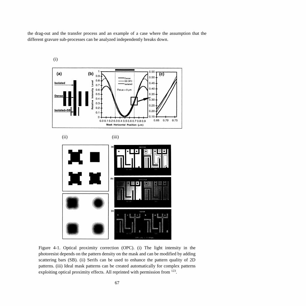
67
the drag-out and the transfer process and an example of a case where the assumption that the
different gravure sub-processes can be analyzed independently breaks down.
(i)
(ii) (iii)
Figure 4-1. Optical proximity correction (OPC). (i) The light intensity in the
photoresist depends on the pattern density on the mask and can be modified by adding
scattering bars (SB). (ii) Serifs can be used to enhance the pattern quality of 2D
patterns. (iii) Ideal mask patterns can be created automatically for complex patterns
exploiting optical proximity effects. All reprinted with permission from 123.

68
At the beginning of this chapter, after a brief overview of the experimental methods, printed
patterns are analyzed on the substrate after ink transfer. The proximity effect is demonstrated and
patterns are evaluated using an automated feature quality extraction method. It is shown how the
proximity effect can be used to enhance print quality. The fluid mechanics of the transfer process
and the proximity effect are studied in detail by measuring ink amounts inside cells before and
after transfer. This insight is used to create a simple model to explain the gravure proximity effect
based on ink flow during the transfer process.
4.2 Experimental
Groups of lines were gravure printed with varying line spacing. Lines were oriented perpendicular
to the printing direction to maximize the impact of the drag-out effect. The cell size was varied
between 2 and 4µm and the spacing or gap between cells within lines was varied between 15 and
60% of the cell size. Lines were one cell wide and the ideal printed linewidth is thus identical with
the cell size. In reality, ink will always spread somewhat to increase linewidth. Figure 4-2
illustrates the pattern variables studied here.
Figure 4-2. Pattern variables studied here: Cell size, cell gap (spacing) and line spacing
Printing results were studied by imaging the final patterns on the plastic substrate. The substrates
were planarized polyethylene naphthalate (PEN) substrates (PQA1) provided by DuPont Teijin
Films. Substrates were treated with a 30 seconds, 50W air plasma before printing to improve ink
transfer. The ink was NPS purchased from Harima Chemicals, a silver nanoparticle ink with 12nm
particle size. A silver ink was chosen due to its reflective optical properties when imaged as well
as its widespread use in the fabrication of printed electrical circuits. The ink viscosity was tuned
by dilution with its solvent AF5. The ink was dried and sintered after printing at 220°C for 120
minutes. After printing, drying and sintering, the printed patterns were imaged by optical
microscopy. The results were analyzed using an automated technique to extract print quality
metrics, namely the fraction of lines merged together, the fraction of discontinuous lines, ink
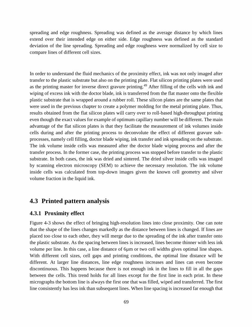
69
spreading and edge roughness. Spreading was defined as the average distance by which lines
extend over their intended edge on either side. Edge roughness was defined as the standard
deviation of the line spreading. Spreading and edge roughness were normalized by cell size to
compare lines of different cell sizes.
In order to understand the fluid mechanics of the proximity effect, ink was not only imaged after
transfer to the plastic substrate but also on the printing plate. Flat silicon printing plates were used
as the printing master for inverse direct gravure printing.49 After filling of the cells with ink and
wiping of excess ink with the doctor blade, ink is transferred from the flat master onto the flexible
plastic substrate that is wrapped around a rubber roll. These silicon plates are the same plates that
were used in the previous chapter to create a polymer molding for the metal printing plate. Thus,
results obtained from the flat silicon plates will carry over to roll-based high-throughput printing
even though the exact values for example of optimum capillary number will be different. The main
advantage of the flat silicon plates is that they facilitate the measurement of ink volumes inside
cells during and after the printing process to deconvolute the effect of different gravure sub-
processes, namely cell filling, doctor blade wiping, ink transfer and ink spreading on the substrate.
The ink volume inside cells was measured after the doctor blade wiping process and after the
transfer process. In the former case, the printing process was stopped before transfer to the plastic
substrate. In both cases, the ink was dried and sintered. The dried silver inside cells was imaged
by scanning electron microscopy (SEM) to achieve the necessary resolution. The ink volume
inside cells was calculated from top-down images given the known cell geometry and silver
volume fraction in the liquid ink.
4.3 Printed pattern analysis
4.3.1 Proximity effect
Figure 4-3 shows the effect of bringing high-resolution lines into close proximity. One can note
that the shape of the lines changes markedly as the distance between lines is changed. If lines are
placed too close to each other, they will merge due to the spreading of the ink after transfer onto
the plastic substrate. As the spacing between lines is increased, lines become thinner with less ink
volume per line. In this case, a line distance of 6µm or two cell widths gives optimal line shapes.
With different cell sizes, cell gaps and printing conditions, the optimal line distance will be
different. At larger line distances, line edge roughness increases and lines can even become
discontinuous. This happens because there is not enough ink in the lines to fill in all the gaps
between the cells. This trend holds for all lines except for the first line in each print. In these
micrographs the bottom line is always the first one that was filled, wiped and transferred. The first
line consistently has less ink than subsequent lines. When line spacing is increased far enough that
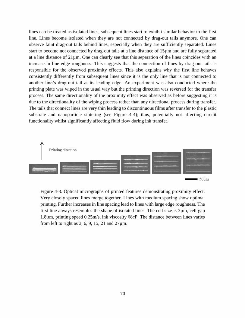
70
lines can be treated as isolated lines, subsequent lines start to exhibit similar behavior to the first
line. Lines become isolated when they are not connected by drag-out tails anymore. One can
observe faint drag-out tails behind lines, especially when they are sufficiently separated. Lines
start to become not connected by drag-out tails at a line distance of 15µm and are fully separated
at a line distance of 21µm. One can clearly see that this separation of the lines coincides with an
increase in line edge roughness. This suggests that the connection of lines by drag-out tails is
responsible for the observed proximity effects. This also explains why the first line behaves
consistently differently from subsequent lines since it is the only line that is not connected to
another line’s drag-out tail at its leading edge. An experiment was also conducted where the
printing plate was wiped in the usual way but the printing direction was reversed for the transfer
process. The same directionality of the proximity effect was observed as before suggesting it is
due to the directionality of the wiping process rather than any directional process during transfer.
The tails that connect lines are very thin leading to discontinuous films after transfer to the plastic
substrate and nanoparticle sintering (see Figure 4-4); thus, potentially not affecting circuit
functionality whilst significantly affecting fluid flow during ink transfer.
Figure 4-3. Optical micrographs of printed features demonstrating proximity effect.
Very closely spaced lines merge together. Lines with medium spacing show optimal
printing. Further increases in line spacing lead to lines with large edge roughness. The
first line always resembles the shape of isolated lines. The cell size is 3µm, cell gap
1.8µm, printing speed 0.25m/s, ink viscosity 68cP. The distance between lines varies
from left to right as 3, 6, 9, 15, 21 and 27µm.
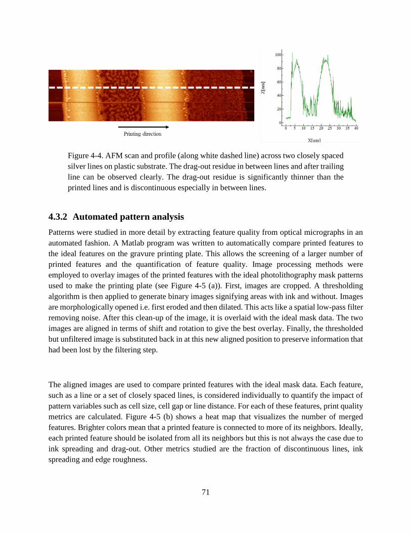
71
Figure 4-4. AFM scan and profile (along white dashed line) across two closely spaced
silver lines on plastic substrate. The drag-out residue in between lines and after trailing
line can be observed clearly. The drag-out residue is significantly thinner than the
printed lines and is discontinuous especially in between lines.
4.3.2 Automated pattern analysis
Patterns were studied in more detail by extracting feature quality from optical micrographs in an
automated fashion. A Matlab program was written to automatically compare printed features to
the ideal features on the gravure printing plate. This allows the screening of a larger number of
printed features and the quantification of feature quality. Image processing methods were
employed to overlay images of the printed features with the ideal photolithography mask patterns
used to make the printing plate (see Figure 4-5 (a)). First, images are cropped. A thresholding
algorithm is then applied to generate binary images signifying areas with ink and without. Images
are morphologically opened i.e. first eroded and then dilated. This acts like a spatial low-pass filter
removing noise. After this clean-up of the image, it is overlaid with the ideal mask data. The two
images are aligned in terms of shift and rotation to give the best overlay. Finally, the thresholded
but unfiltered image is substituted back in at this new aligned position to preserve information that
had been lost by the filtering step.
The aligned images are used to compare printed features with the ideal mask data. Each feature,
such as a line or a set of closely spaced lines, is considered individually to quantify the impact of
pattern variables such as cell size, cell gap or line distance. For each of these features, print quality
metrics are calculated. Figure 4-5 (b) shows a heat map that visualizes the number of merged
features. Brighter colors mean that a printed feature is connected to more of its neighbors. Ideally,
each printed feature should be isolated from all its neighbors but this is not always the case due to
ink spreading and drag-out. Other metrics studied are the fraction of discontinuous lines, ink
spreading and edge roughness.

72
Figure 4-5. Feature extraction and evaluation algorithm (a) Alignment of printed
features with ideal mask data. (i) Original image of printed features. (ii) Printed
features after cropping, thresholding and filtering. (iii) Mask data (blue) overlaid on
top of printed features (green). (iv) Final alignment of printed features and mask data.
Overlapping areas are colored red. The original unfiltered but thresholded image was
substituted back in to increase accuracy of feature evaluation. (b) Feature quality
evaluation. (i) Aligned printed features and mask data (same stage as panel a iv). (ii)
Heat map of one feature quality metric: feature merging. The brighter the color, the
larger the number of other features a particular feature is connected with due to non-
ideal printing.
73
4.3.3 Design rules and assist features
The automated extraction of print quality metrics allows the screening of different parameters,
both printing conditions including ink properties as well as pattern variables, to identify design
rules for particular situations. Here, closely spaced lines printed perpendicular to the printing
direction are taken as an example. First, ink viscosity was varied whilst keeping Ca constant to
study the effect of ink spreading on the substrate independently from the other gravure sub-
processes and to find the optimum viscosity for these patterns (see Figure 4-6). The lower the ink
viscosity, the easier it will be for the ink to spread on the substrate. The lowest viscosity ink studied
here at 34cP spreads the most. This limits the minimum feature size that can be achieved, both in
terms of line width, as well as minimum line spacing. Lines printed with low viscosity inks are
more prone to merge together. In an electrical circuit, this would result in a short circuit, which
would be a fatal flaw destroying the functionality of the circuit. A design rule must thus take ink
spreading into account and put a lower limit on line spacing to achieve reliably separated lines.
This minimum line spacing will be larger for the 34cP ink than for the other inks studied here.
Thus the 34cP ink is not optimal. On the other hand, if the viscosity is too high, there is not enough
spreading. Gravure relies on ink spreading to fill in the gaps between discrete cells and form
continuous lines. If the ink does not spread enough, line edge roughness increases. There will be
less ink in the cell gaps in between cells leading to scalloped lines where the wavelength of the
scallops corresponds to the placement of cells. In the more extreme case, lines can become
discontinuous leading to open circuits. This is another fatal flaw that would render a circuit
unusable. The highest viscosity ink studied here at 195cP shows both increased line edge
roughness as well as a much larger fraction of discontinuous lines. This is especially true for lines
spaced further apart that don’t get the benefit of the proximity effect. 68cP was found to be the
optimum ink viscosity for the patterns studied here leading to the optimum amount of spreading
that minimizes both the merging of adjacent lines and the number of discontinuous lines. This
viscosity was used to study the effect of printing speed and cell gap.
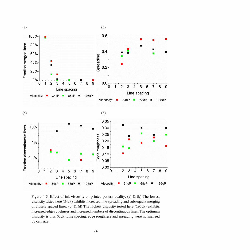
74
(a) (b)
(c) (d)
Figure 4-6. Effect of ink viscosity on printed pattern quality. (a) & (b) The lowest
viscosity tested here (34cP) exhibits increased line spreading and subsequent merging
of closely spaced lines. (c) & (d) The highest viscosity tested here (195cP) exhibits
increased edge roughness and increased numbers of discontinuous lines. The optimum
viscosity is thus 68cP. Line spacing, edge roughness and spreading were normalized
by cell size.

75
The interaction between printing speed, cell gap, cell size and line spacing is complex. The main
competing effects are drag-out, proximity effects and lubrication residue. Drag-out occurs due to
ink wicking up the doctor blade. This is driven by surface tension forces and is inhibited by viscous
forces. Drag-out therefore becomes more severe at smaller capillary numbers. Drag-out also
becomes more severe for smaller cells because a larger fraction of the ink in the cell can be
dragged-out by the doctor blade. The relationship between the proximity effect and the capillary
number is non-monotonic and will be analyzed in detail in the next section. Lubrication residue
becomes more severe at high printing speeds and viscosities. This film is due to ink that passes
under the doctor blade. The fluid pressure in this gap between the doctor blade and the printing
plate balances the loading force on the doctor blade. This pressure increases with viscosity and
speed leading to thicker residue films. In theory, this residue is deposited uniformly across the
printing plate; however, in practice residue is concentrated in areas of doctor blade defects due to
wear. The impact of this on yield will be discussed further in the next chapter. These different
effects control the amount of ink left in the cells after wiping. When trying to print ideal lines, one
needs to have the ideal amount of ink per unit length. If the amount of ink per unit length is too
large, lines will bulge, become non-uniform and ultimately merge with adjacent lines. If there is
not enough ink, lines will become scalloped and ultimately break up. The amount of ink per unit
length is not only governed by the amount of ink inside cells but also by the cell spacing within
each line. If cells are spaced further apart, there is less ink per unit length and vice versa. Thus it
is important to have the optimum amount of ink inside the cells combined with the right cell
spacing. These considerations are similar to previous work on inkjet printed lines, although in a
higher viscosity regime and with simultaneous printing of all droplets that make up a line.57
The goal of understanding these processes is to create design rules that can be used to make choices
when designing gravure printed circuits. A principal challenge is that printing conditions such as
speed and viscosity apply globally to all patterns printed at the same time. If a circuit contains a
diverse set of patterns such as different line widths and separations, these different patterns might
require different conditions for optimal printing. The designer has the freedom to change the cell
spacing to tune the optimal conditions for a particular pattern and ameliorate conflicts but the scope
of this is limited. Consider the case where a design includes a set of closely space 4µm lines, such
as bus lines packed tightly into a confined area, as well as isolated 2µm lines, such as in a sparse
grid. Representative printing results and extracted print quality metrics for these cases can be found
in Figure 4-7 and Figure 4-8 respectively. The closely spaced 4µm lines show optimum line edge
roughness at low printing speeds, especially 0.25m/s. At higher printing speeds drag-out becomes
less pronounced leading to a larger amount of ink inside the cells. There is also more lubrication
residue at higher printing speeds. This leads to excessive and uneven spreading of lines and can
even result in lines merging together. Conversely, isolated 2µm lines print best at high printing
speeds of 0.5m/s or 1m/s. At lower printing speeds drag-out pulls too much ink out of these small
cells. This leads to scalloped edges and even discontinuous lines. This is the case even though cell

76
spacing was already optimized for both cell sizes for the respective conditions. This simple
example shows the difficulties when trying to print a diverse set of high-resolution patterns and
will only get worse with more complex circuits. Since global printing conditions need to work for
all patterns in a print, local patterns need to be adapted to make them compatible. Assist features
exploiting proximity effects can be one method to achieve this.
Figure 4-7. Optical micrographs of closely spaced lines with 4µm cell size and 8µm
line spacing (first row (a)-(d)) and isolated lines with 2µm cell size (second row (e)-
(h)). In both rows, printing speed increases from left to right as 0.125m/s, 0.25m/s,
0.5m/s and 1.0m/s. These two cases exhibit opposite trends of print quality with
printing speed. Closely spaced 4µm lines exhibit better line definition with slower
speed whereas isolated 2µm lines need to be printed at higher speeds.

77
(a) (b)
Figure 4-8. (a) Fraction of merged lines increases with increasing printing speed for
lines with 4µm cell size that are closely spaced 8µm apart. (b) Edge roughness drops
with increasing printing speed for isolated lines with 2µm cell size. Edge roughness
was normalized by cell size.
Optical lithography uses assist structures to print high-resolution features. This method exploits
optical proximity effects. Sub-resolution features such as scattering bars are placed next to the
feature to be printed. For isolated lines, this simulates the situation of densely spaced lines. Even
though the assist feature does not print itself, its wave function can constructively interfere with
the wave function of the actual feature and assist in its printing. Here, a similar method is proposed
for gravure printing to exploit fluidic proximity effects. The real feature is placed behind the assist
feature so that it is located inside the assist feature’s drag-out tail. This will add ink to the real
feature and make it printable. Here, assist features are employed that are of the same size as the
real feature to be printed. The print quality of the assist feature is lower because it is not supported
by the proximity effect but it will still be printed. In the future, more sophisticated assist features
could be explored that don’t transfer or only transfer minimally to the final substrate. This concept
of fluidic assist features is demonstrated with the example of isolated high-resolution 2µm lines
oriented perpendicular to the printing direction. Such lines cannot be printed easily at low printing
speeds around 0.25m/s. Lines tend to break up due to excessive drag-out. With the extra ink from
the assist feature, such lines can successfully be printed. The result can be observed in Figure 4-9.
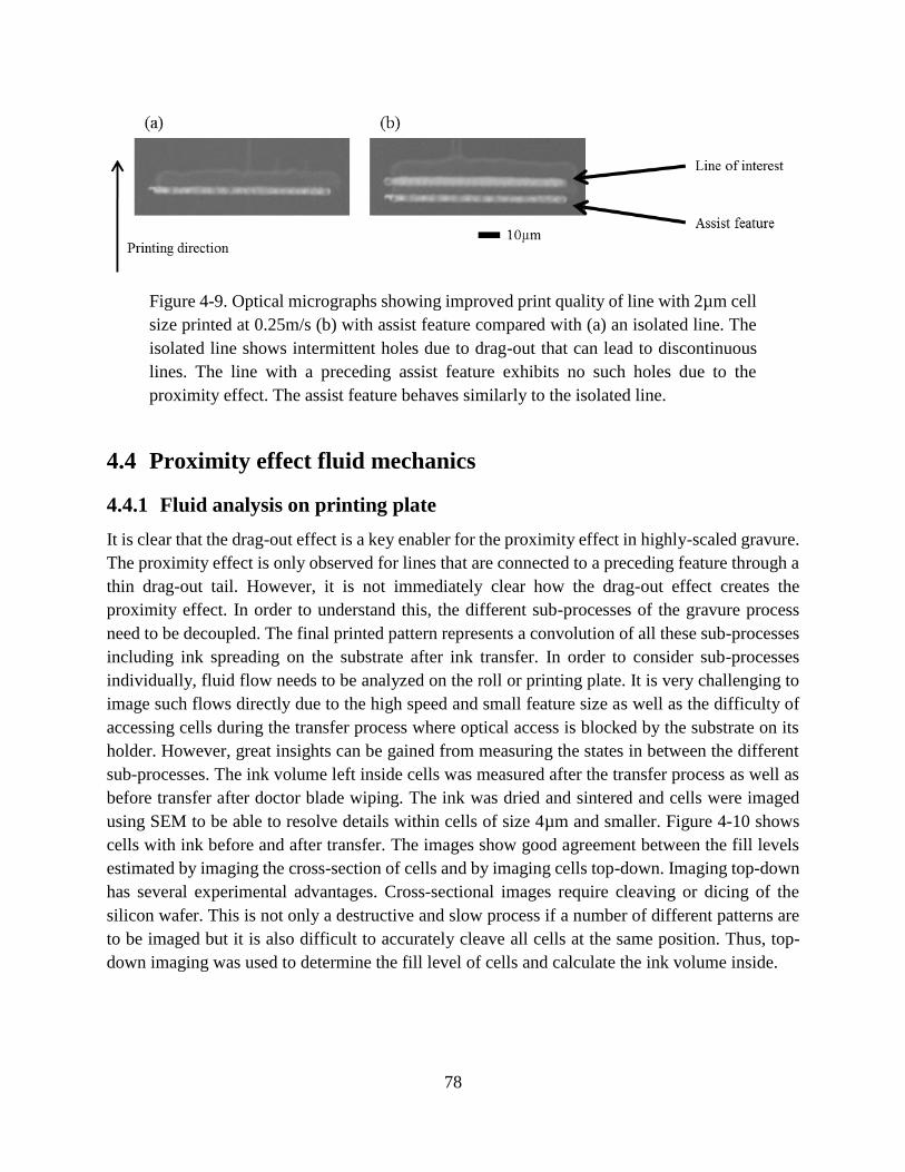
78
Figure 4-9. Optical micrographs showing improved print quality of line with 2µm cell
size printed at 0.25m/s (b) with assist feature compared with (a) an isolated line. The
isolated line shows intermittent holes due to drag-out that can lead to discontinuous
lines. The line with a preceding assist feature exhibits no such holes due to the
proximity effect. The assist feature behaves similarly to the isolated line.
4.4 Proximity effect fluid mechanics
4.4.1 Fluid analysis on printing plate
It is clear that the drag-out effect is a key enabler for the proximity effect in highly-scaled gravure.
The proximity effect is only observed for lines that are connected to a preceding feature through a
thin drag-out tail. However, it is not immediately clear how the drag-out effect creates the
proximity effect. In order to understand this, the different sub-processes of the gravure process
need to be decoupled. The final printed pattern represents a convolution of all these sub-processes
including ink spreading on the substrate after ink transfer. In order to consider sub-processes
individually, fluid flow needs to be analyzed on the roll or printing plate. It is very challenging to
image such flows directly due to the high speed and small feature size as well as the difficulty of
accessing cells during the transfer process where optical access is blocked by the substrate on its
holder. However, great insights can be gained from measuring the states in between the different
sub-processes. The ink volume left inside cells was measured after the transfer process as well as
before transfer after doctor blade wiping. The ink was dried and sintered and cells were imaged
using SEM to be able to resolve details within cells of size 4µm and smaller. Figure 4-10 shows
cells with ink before and after transfer. The images show good agreement between the fill levels
estimated by imaging the cross-section of cells and by imaging cells top-down. Imaging top-down
has several experimental advantages. Cross-sectional images require cleaving or dicing of the
silicon wafer. This is not only a destructive and slow process if a number of different patterns are
to be imaged but it is also difficult to accurately cleave all cells at the same position. Thus, top-
down imaging was used to determine the fill level of cells and calculate the ink volume inside.
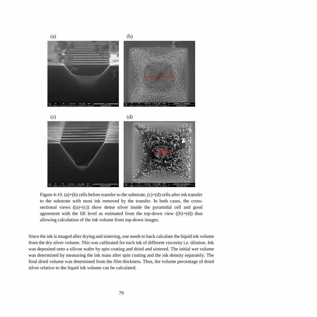
79
Figure 4-10. (a)+(b) cells before transfer to the substrate, (c)+(d) cells after ink transfer
to the substrate with most ink removed by the transfer. In both cases, the cross-
sectional views ((a)+(c)) show dense silver inside the pyramidal cell and good
agreement with the fill level as estimated from the top-down view ((b)+(d)) thus
allowing calculation of the ink volume from top-down images.
Since the ink is imaged after drying and sintering, one needs to back calculate the liquid ink volume
from the dry silver volume. This was calibrated for each ink of different viscosity i.e. dilution. Ink
was deposited onto a silicon wafer by spin coating and dried and sintered. The initial wet volume
was determined by measuring the ink mass after spin coating and the ink density separately. The
final dried volume was determined from the film thickness. Thus, the volume percentage of dried
silver relative to the liquid ink volume can be calculated.
80
4.4.2 Ink transfer
As a first step, ink transfer from isolated lines without proximity effects was studied. Ink transfer
is the most well studied gravure sub-process.69–81 However, most reports have focused on transfer
as an isolated process i.e. transfer of a liquid from a flat surface or a cell onto a flat substrate
without taking into consideration how the initial state of the liquid on a roll or printing plate is
achieved. In the full gravure process, the starting state for the transfer process is determined by the
previous cell filling and doctor blade wiping processes. Since all three processes depend on
capillary number, they cannot easily be altered independently. This is demonstrated here by using
the ink volumes measured inside cells before and after transfer.
Figure 4-11 shows the transfer fraction as a function of capillary number. The transfer fraction is
defined as
𝜑𝑡𝑟𝑎𝑛𝑠𝑓𝑒𝑟 =𝑉𝑡𝑟𝑎𝑛𝑠𝑓𝑒𝑟
𝑉𝑤𝑖𝑝𝑖𝑛𝑔=
𝑉𝑤𝑖𝑝𝑖𝑛𝑔−𝑉𝑐𝑒𝑙𝑙 𝑡𝑟𝑎𝑛𝑠𝑓𝑒𝑟
𝑉𝑤𝑖𝑝𝑖𝑛𝑔 Eq. 4-1
Where Vwiping is the ink volume left in the cell after doctor blade wiping, Vtransfer is the ink volume
transferred to the substrate and Vcell transfer is the ink volume left in the cell after transfer, which can
be measured more easily than Vtransfer. At low values of Ca, transfer is almost perfect with almost
all the ink transferring from the cell to the substrate. This can be explained by the different wetting
properties of the printing plate and the substrate.76 The printing plate is a silicon wafer with very
small contact angle hysteresis whereas the coating of the PEN plastic substrate has been optimized
to increase pinning and contact angle hysteresis. This means the contact line is more prone to
recede on the printing plate than on the substrate. If there is enough time for this to happen, all ink
is removed from the cell and transfer is perfect. This is the case at low values of capillary number.
At higher values of capillary number, there is not enough time for the contact line to move before
the liquid bridge between the printing plate and the substrate breaks off. Thus, the transfer fraction
should level off around 0.5 for high values of Ca. This is observed around Ca=1.
However; at values of Ca larger than 1, another regime is observed where transfer fraction
increases with Ca. This can be understood in terms of the initial ink volume inside the cell before
transfer. Transfer is facilitated by increased initial fill levels.71 Figure 4-12 shows the fill fraction
before transfer as a function of capillary number. Initially, fill fraction increases with Ca because
of decreased drag-out. The dominance of drag-out in this regime can also be seen from the length
of the drag-out tails (see Figure 4-13). Especially at very small values of Ca, drag-out becomes
excessive. In this regime, the transfer fraction drops off for very small values of Ca because there
is not enough ink inside the cell to be effectively picked out from the cell. Then, at intermediate
values of Ca, fill fraction decreases slightly because of decreased cell filling. Finally, at high values

81
of Ca, fill fraction increases again with Ca due to increased lubrication residue.49 This increase in
fill fraction before transfer leads to an increased transfer fraction for large values of Ca.
Figure 4-11. Transfer fraction for isolated lines with different cell sizes versus
capillary number. At very low values of Ca, transfer fraction drops off. It then stays
constant with Ca and almost perfect until it decreases at intermediate values of Ca.
Transfer fraction increases again in the high Ca regime.
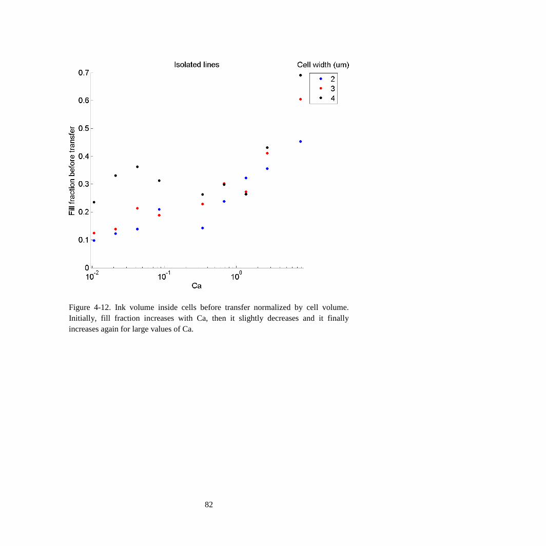
82
Figure 4-12. Ink volume inside cells before transfer normalized by cell volume.
Initially, fill fraction increases with Ca, then it slightly decreases and it finally
increases again for large values of Ca.
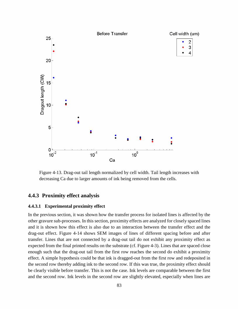
83
Figure 4-13. Drag-out tail length normalized by cell width. Tail length increases with
decreasing Ca due to larger amounts of ink being removed from the cells.
4.4.3 Proximity effect analysis
4.4.3.1 Experimental proximity effect
In the previous section, it was shown how the transfer process for isolated lines is affected by the
other gravure sub-processes. In this section, proximity effects are analyzed for closely spaced lines
and it is shown how this effect is also due to an interaction between the transfer effect and the
drag-out effect. Figure 4-14 shows SEM images of lines of different spacing before and after
transfer. Lines that are not connected by a drag-out tail do not exhibit any proximity effect as
expected from the final printed results on the substrate (cf. Figure 4-3). Lines that are spaced close
enough such that the drag-out tail from the first row reaches the second do exhibit a proximity
effect. A simple hypothesis could be that ink is dragged-out from the first row and redeposited in
the second row thereby adding ink to the second row. If this was true, the proximity effect should
be clearly visible before transfer. This is not the case. Ink levels are comparable between the first
and the second row. Ink levels in the second row are slightly elevated, especially when lines are
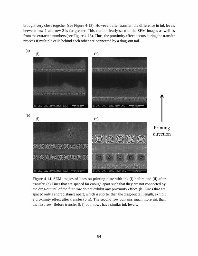
84
brought very close together (see Figure 4-15). However; after transfer, the difference in ink levels
between row 1 and row 2 is far greater. This can be clearly seen in the SEM images as well as
from the extracted numbers (see Figure 4-16). Thus, the proximity effect occurs during the transfer
process if multiple cells behind each other are connected by a drag-out tail.
Figure 4-14. SEM images of lines on printing plate with ink (i) before and (ii) after
transfer. (a) Lines that are spaced far enough apart such that they are not connected by
the drag-out tail of the first row do not exhibit any proximity effect. (b) Lines that are
spaced only a short distance apart, which is shorter than the drag-out tail length, exhibit
a proximity effect after transfer (b ii). The second row contains much more ink than
the first row. Before transfer (b i) both rows have similar ink levels.

85
Figure 4-15. Ratio between ink volume in second row and ink volume in first row
before transfer i.e. after doctor blade wiping and drag-out. As lines are brought close
together, dragged-out ink from the first row is redeposited in the second row. Line
spacing is normalized by the length of the drag-out tails before transfer to account for
the fact that different capillary numbers exhibit different drag-out lengths.
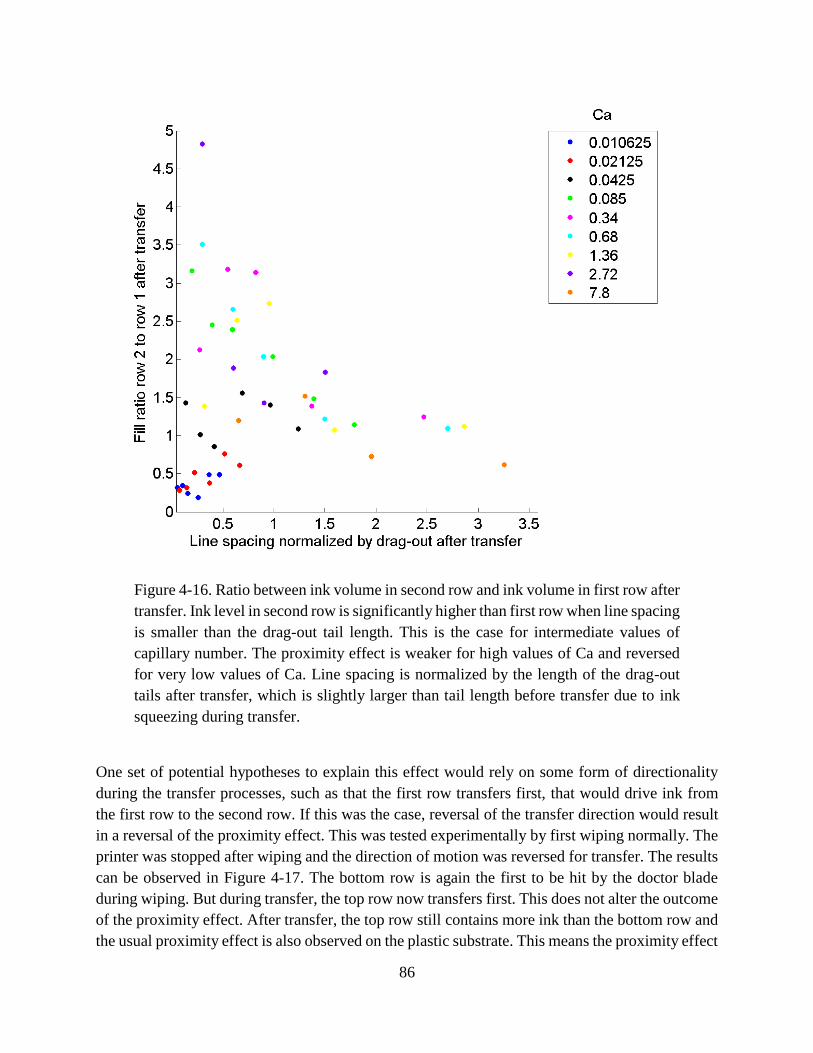
86
Figure 4-16. Ratio between ink volume in second row and ink volume in first row after
transfer. Ink level in second row is significantly higher than first row when line spacing
is smaller than the drag-out tail length. This is the case for intermediate values of
capillary number. The proximity effect is weaker for high values of Ca and reversed
for very low values of Ca. Line spacing is normalized by the length of the drag-out
tails after transfer, which is slightly larger than tail length before transfer due to ink
squeezing during transfer.
One set of potential hypotheses to explain this effect would rely on some form of directionality
during the transfer processes, such as that the first row transfers first, that would drive ink from
the first row to the second row. If this was the case, reversal of the transfer direction would result
in a reversal of the proximity effect. This was tested experimentally by first wiping normally. The
printer was stopped after wiping and the direction of motion was reversed for transfer. The results
can be observed in Figure 4-17. The bottom row is again the first to be hit by the doctor blade
during wiping. But during transfer, the top row now transfers first. This does not alter the outcome
of the proximity effect. After transfer, the top row still contains more ink than the bottom row and
the usual proximity effect is also observed on the plastic substrate. This means the proximity effect
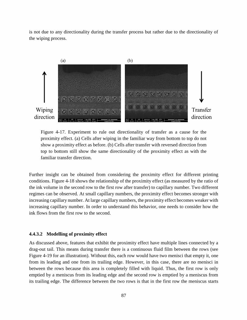
87
is not due to any directionality during the transfer process but rather due to the directionality of
the wiping process.
Figure 4-17. Experiment to rule out directionality of transfer as a cause for the
proximity effect. (a) Cells after wiping in the familiar way from bottom to top do not
show a proximity effect as before. (b) Cells after transfer with reversed direction from
top to bottom still show the same directionality of the proximity effect as with the
familiar transfer direction.
Further insight can be obtained from considering the proximity effect for different printing
conditions. Figure 4-18 shows the relationship of the proximity effect (as measured by the ratio of
the ink volume in the second row to the first row after transfer) to capillary number. Two different
regimes can be observed. At small capillary numbers, the proximity effect becomes stronger with
increasing capillary number. At large capillary numbers, the proximity effect becomes weaker with
increasing capillary number. In order to understand this behavior, one needs to consider how the
ink flows from the first row to the second.
4.4.3.2 Modelling of proximity effect
As discussed above, features that exhibit the proximity effect have multiple lines connected by a
drag-out tail. This means during transfer there is a continuous fluid film between the rows (see
Figure 4-19 for an illustration). Without this, each row would have two menisci that empty it, one
from its leading and one from its trailing edge. However, in this case, there are no menisci in
between the rows because this area is completely filled with liquid. Thus, the first row is only
emptied by a meniscus from its leading edge and the second row is emptied by a meniscus from
its trailing edge. The difference between the two rows is that in the first row the meniscus starts

88
right at the cell whereas in the second row it starts at the end of the drag-out tail. In order to
understand how this affects fluid flow, a simple 2D model was created.
Figure 4-18. The proximity effect (ink volume ratio between row 2 and row 1 after
transfer) shows two regimes with capillary number and a maximum at an intermediate
value of Ca.

89
Figure 4-19. Cross-sectional schematic of transfer process with proximity effect. (a)
Two rows are connected by drag-out tails. Substrate approaches printing plate. (b)
Substrate is in contact with printing plate. (c) Substrate is removed from printing plate
and both rows are emptied by menisci that move inwards. (d) After breakup of the
liquid bridge, ink transfer is complete and more ink is left in the second row both on
the substrate and the printing plate.
The flow in the channel that is formed in between the substrate and the printing plate during
transfer is described here as a pressure driven Poiseuille flow. Solving the Navier-Stokes equation
by approximating the situation as a thin channel between parallel plates gives the familiar result
for flow rate along the channel per unit width into the page qx as
𝑞𝑥 = −ℎ3
12𝜇
𝑑𝑝
𝑑𝑥 Eq. 4-2
Where h is the channel height at a particular position x along the channel, µ is the fluid viscosity
and p is the pressure, which is also a function of x. Here, flow not only occurs along the channel
direction but also due to the substrate moving upwards away from the printing plate. For a small
fluid element of width δx, this can be modelled as a vertical flow rate
𝑞𝑧 = 𝑣𝑧 ∗ 𝛿𝑥 Eq. 4-3
Where vz is the vertical velocity of the substrate. Balancing the vertical and horizontal flow
components on a fluid element and conserving mass leads to the following differential equations
−𝑑𝑞𝑥
𝑑𝑥= 𝑣𝑧 Eq. 4-4
𝑑
𝑑𝑥(ℎ3 𝑑𝑝
𝑑𝑥) = 12𝜇𝑣𝑧 Eq. 4-5
Integrating twice results in the following expression for the pressure p

90
𝑝(𝑥) = 12𝜇𝑣𝑧 ∫𝑥
ℎ3𝑑𝑥
𝑥
0+ ℎ3(0)
𝑑𝑝
𝑑𝑥(0) ∫
1
ℎ3𝑑𝑥
𝑥
0+ 𝑝(0) Eq. 4-6
The derivative of the pressure at x=0 can be calculated using the pressures at the two menisci as
boundary conditions giving
𝑑𝑝
𝑑𝑥(0) =
1
ℎ3(0) ∫1
ℎ3𝑑𝑥𝐿
0
(𝑝(𝐿) − 𝑝(0) − 12𝜇𝑣𝑧 ∫𝑥
ℎ3𝑑𝑥
𝐿
0) Eq. 4-7
The position of the first row’s meniscus is defined as x=0 and the position of the second row’s
meniscus is defined as x=L. The two meniscus pressures can be estimated by assuming a circular
meniscus cross-section with radius of curvature h/2 giving
𝑝(0) =𝛾
ℎ(0)2
Eq. 4-8
And similarly for p(L). γ is the ink surface tension. This set of equations allows the calculation of
the pressure profile along the channel that is formed between the roll and the substrate.
Figure 4-20 shows the profile of two cells connected by a thin fluid film and with another thin
drag-out film after the second cell. The pressure profile for this situation exhibits a parabolic shape
in the regions with a thin uniform fluid film as expected (see Figure 4-21). The pressure drop
across the cells is negligible compared with the pressure drop across the thin regions. Continuity
dictates that the flow rate is a linear function of position due to the constant upward flow caused
by the motion of the substrate (see Figure 4-22). However, the flow is not symmetric. There is a
larger inward flow at the first cell compared with the end of the drag-out tail (with reversed
direction). This is due to the fact that the meniscus at the first cell is immediately adjacent to a cell
whereas the second meniscus is adjacent to a long thin region. The thick fluid film in the cell poses
less resistance to fluid flow as can be seen from the negligible pressure drop across it. This is the
reason for the proximity effect resulting in net fluid flow towards the second row. This imbalance
in flow between the first and the second row can be described as the ratio between the two flows
and this measure of the proximity effect can be analyzed to understand the experimental results.
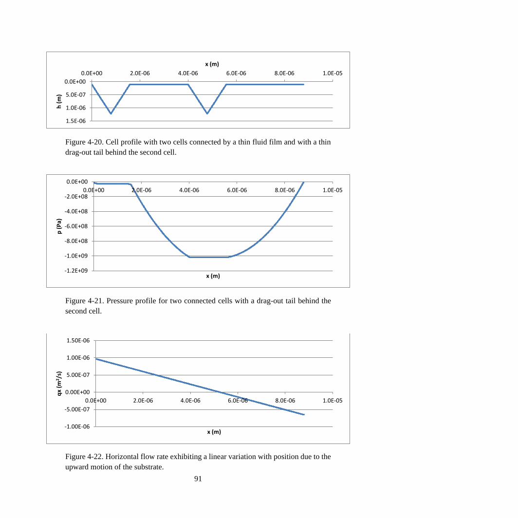
91
Figure 4-20. Cell profile with two cells connected by a thin fluid film and with a thin
drag-out tail behind the second cell.
Figure 4-21. Pressure profile for two connected cells with a drag-out tail behind the
second cell.
Figure 4-22. Horizontal flow rate exhibiting a linear variation with position due to the
upward motion of the substrate.
0.0E+00
5.0E-07
1.0E-06
1.5E-06
0.0E+00 2.0E-06 4.0E-06 6.0E-06 8.0E-06 1.0E-05
h (
m)
x (m)
-1.2E+09
-1.0E+09
-8.0E+08
-6.0E+08
-4.0E+08
-2.0E+08
0.0E+00
0.0E+00 2.0E-06 4.0E-06 6.0E-06 8.0E-06 1.0E-05
p (
Pa)
x (m)
-1.00E-06
-5.00E-07
0.00E+00
5.00E-07
1.00E-06
1.50E-06
0.0E+00 2.0E-06 4.0E-06 6.0E-06 8.0E-06 1.0E-05
qx
(m2 /
s)
x (m)

92
Experimental results show a strong effect of capillary number on the proximity effect (cf. Figure
4-18). The obvious question is thus how print speed, ink viscosity and ink surface tension affect
the flow that is responsible for the proximity effect during transfer. Whilst speed and viscosity
certainly affect the flow, they do not affect the imbalance in flow between the two menisci. Both
are equally affected by the product of speed and viscosity as can be seen in Eq. 4-6. Surface tension
could in principle affect the two menisci differently if they exhibit different radii of curvature.
However; for realistic values of surface tension well below 100mN/m, the meniscus pressure due
to surface tension is very small compared with the pressure drop across the channel due to the
flow. This can be observed in Figure 4-21 where the pressures at either end are negligible. Thus,
the capillary number dependence of the proximity effect is not directly due to differences in speed,
viscosity or surface tension. However, these variables affect the initial state i.e. the fluid geometry
before transfer.
Conceivably, the thickness of the thin fluid regions between the cells and behind the second cell
could affect flow. However, its effect on the proximity effect is weak and only becomes apparent
as the film thickness becomes larger than 100nm and approaches 1µm (see Figure 4-23). The
reason is that for thin films the pressure drop across cells remains negligible irrespective of the
exact film thickness. The magnitude of the observed pressure changes but does so equally for both
menisci and thus does not affect the proximity effect. For thicker films, the pressure drop across
the thin regions drops and becomes comparable to the pressure drop across the cells. Thus, the
effect of having a cell close to the first meniscus diminishes. However, such thick drag-out film
thicknesses are typically not observed experimentally and so the effect of gap height can be
ignored.

93
Figure 4-23. The proximity effect does not depend on the gap height between the
substrate and the roll in the land areas i.e. in between lines and in the drag-out tail as
long as it remains thin compared with the cell size (here 2µm cell width).
The drag-out tail length is another geometrical variable that is determined by the drag-out process
and varies with capillary number. Figure 4-24 shows that the strength of the proximity effect does
depend on drag-out tail length. The proximity effect is strongest for relatively short drag-out tails
of similar length as the cell width. The proximity effect is reduced dramatically for very short tails
as this situation approaches the symmetric case without any drag-out tail behind the second row.
The proximity effect drops off more slowly for longer tails. In this case, the flow becomes
dominated by the long thin fluid region behind the second cell and the effect of the cells diminishes
in comparison. In principle, this peak in the strength of the proximity effect with tail length could
explain the experimentally observed peak with capillary number. The drop in proximity effect with
increasing tail length can contribute to the drop with decreasing capillary number. However, in the
present set of experiments even the highest capillary number resulted in drag-out tails whose length
was at least 1.5 times the cell width and thus too long to observe a drop in proximity effect due to
short tails (cf. Figure 4-13).
0
0.2
0.4
0.6
0.8
1
1.2
1.4
1.6
1.8
2
1.0E-09 1.0E-08 1.0E-07 1.0E-06
Flo
w r
atio
ro
w 2
to
ro
w 1
Gap height (m)
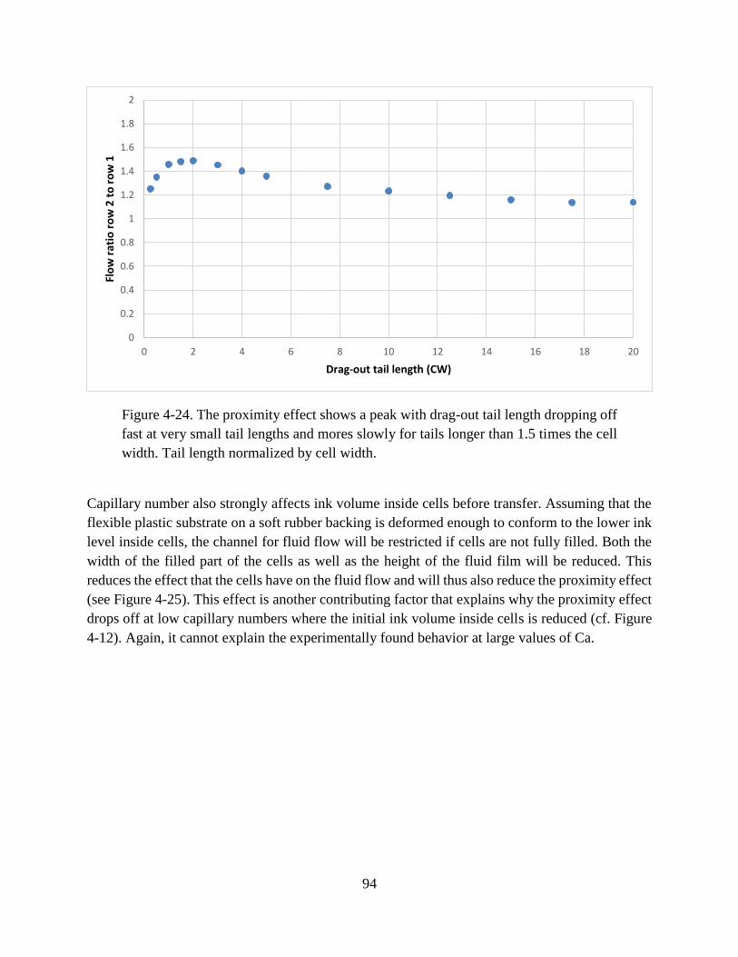
94
Figure 4-24. The proximity effect shows a peak with drag-out tail length dropping off
fast at very small tail lengths and mores slowly for tails longer than 1.5 times the cell
width. Tail length normalized by cell width.
Capillary number also strongly affects ink volume inside cells before transfer. Assuming that the
flexible plastic substrate on a soft rubber backing is deformed enough to conform to the lower ink
level inside cells, the channel for fluid flow will be restricted if cells are not fully filled. Both the
width of the filled part of the cells as well as the height of the fluid film will be reduced. This
reduces the effect that the cells have on the fluid flow and will thus also reduce the proximity effect
(see Figure 4-25). This effect is another contributing factor that explains why the proximity effect
drops off at low capillary numbers where the initial ink volume inside cells is reduced (cf. Figure
4-12). Again, it cannot explain the experimentally found behavior at large values of Ca.
0
0.2
0.4
0.6
0.8
1
1.2
1.4
1.6
1.8
2
0 2 4 6 8 10 12 14 16 18 20
Flo
w r
atio
ro
w 2
to
ro
w 1
Drag-out tail length (CW)

95
Figure 4-25. The proximity effect increases with ink volume inside cells before
transfer. Both cells have equal fill levels here.
In the above figures, one variable was varied at a time to gain understanding of the underlying
mechanisms. They were put together by taking the experimentally measured conditions before
transfer and putting them into the model. Figure 4-26 shows the expected trend of increasing
proximity effect with increasing capillary number. This describes the experimental trend for small
capillary numbers. For large capillary numbers, one needs to consider 3D effects that are not
captured by this 2D model.
0
0.2
0.4
0.6
0.8
1
1.2
1.4
1.6
1.8
2
0% 10% 20% 30% 40% 50% 60% 70% 80% 90% 100%
Flo
w r
atio
ro
w 2
to
ro
w 1
Fill fraction before transfer
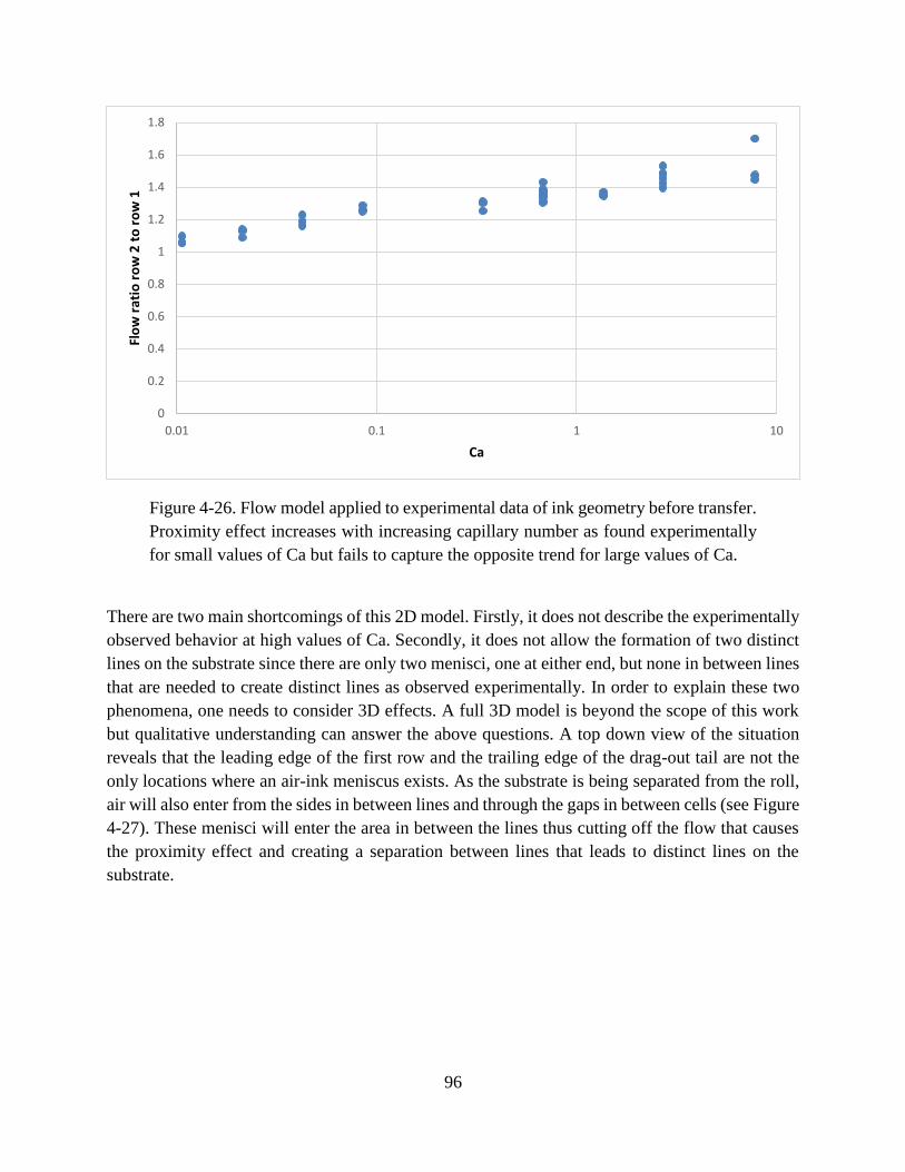
96
Figure 4-26. Flow model applied to experimental data of ink geometry before transfer.
Proximity effect increases with increasing capillary number as found experimentally
for small values of Ca but fails to capture the opposite trend for large values of Ca.
There are two main shortcomings of this 2D model. Firstly, it does not describe the experimentally
observed behavior at high values of Ca. Secondly, it does not allow the formation of two distinct
lines on the substrate since there are only two menisci, one at either end, but none in between lines
that are needed to create distinct lines as observed experimentally. In order to explain these two
phenomena, one needs to consider 3D effects. A full 3D model is beyond the scope of this work
but qualitative understanding can answer the above questions. A top down view of the situation
reveals that the leading edge of the first row and the trailing edge of the drag-out tail are not the
only locations where an air-ink meniscus exists. As the substrate is being separated from the roll,
air will also enter from the sides in between lines and through the gaps in between cells (see Figure
4-27). These menisci will enter the area in between the lines thus cutting off the flow that causes
the proximity effect and creating a separation between lines that leads to distinct lines on the
substrate.
0
0.2
0.4
0.6
0.8
1
1.2
1.4
1.6
1.8
0.01 0.1 1 10
Flo
w r
atio
ro
w 2
to
ro
w 1
Ca

97
Figure 4-27. Top down view of ink transfer. Air enters the fluid (yellow) that is
sandwiched between the roll and the substrate not only through cells (blue) and the
drag-out tail but also from the sides in between rows and though the gaps in between
cells.
In order to do so, these menisci need to move faster than the meniscus that empties the cells in the
first row. This can occur because of the Saffman-Taylor instability leading to viscous
fingering.125,126 The Saffman-Taylor instability occurs at interfaces where a low viscosity fluid
(here: air) penetrates a thin, confined film of a high viscosity fluid (here: ink). Any small
disturbances in the interface grow due to the difference in pressure gradient in the ink between the
tip and the base of air fingers penetrating the ink. The larger pressure gradient at the tip of the
fingers accelerates the growth of fingers ultimately leading to a small number of long air fingers
penetrating the ink. This phenomenon has been observed in gravure printing as well as other roll
based transfer processes.127–130 The growth of these fingers is greatly enhanced for thinner fluid
films. This allows the meniscus to grow faster in the regions with a thin fluid film outside of the
cells, to overtake the menisci inside cells and to cut them off in between rows. If this hypothesis
is to be true, one would expect the size of the gaps between cells as well as position relative to the
end of the lines to be important factors. Positions closer to the end of the lines will experience air
coming in from the sides first and thus the proximity effect flow will be cut off sooner. Similarly,
wider cell gaps will result in enhanced influx of air that cuts off the proximity effect sooner. Both
effects are observed experimentally. Both wider cell gaps and a position closer to the end of the
lines result in a diminished proximity effect (see Figure 4-28 and Figure 4-29). The Saffman-
Taylor instability also explains the observed effect of capillary number for large values of Ca.
Large values of Ca lead to thinner air fingers penetrating the viscous ink and thus faster
advancement of the meniscus due to continuity.126 Figure 4-30 shows how more ink is removed
from the area in between lines as capillary number increases. Thus, the proximity effect flow is
cut off faster for larger values of Ca giving the observed experimental trend.
In conclusion, the proximity effect can be explained by the difference in resistance to flow at the
leading and the trailing edge of the pattern. The cells close to the meniscus at the leading edge
exhibit a smaller resistance to flow than the thin drag-out tail at the trailing edge. At small capillary

98
numbers, the proximity effect is limited by long drag-out tails dominating the flow and by reduced
ink amounts inside cells not exhibiting low resistance to flow. At large capillary numbers, the
proximity effect is limited by viscous fingering through the cell gaps that cuts off the proximity
effect flow in between lines.
Figure 4-28. The proximity effect diminishes close to the end of the lines because this
flow is cut off by air entering from the sides. Distance from end normalized by cell
width.
Figure 4-29. The proximity effect diminishes for large gaps between cells because air
can easily enter region between lines cutting off proximity effect flow. Cell gap
normalized by cell width.
0.00
1.00
2.00
3.00
4.00
5.00
6.00
7.00
8.00
0 1 2 3 4 5 6 7
Fill
rati
o r
ow
2 /
ro
w 1
aft
er
tran
sfe
r
End distance (CW)
0
1
2
3
4
5
6
0 0.1 0.2 0.3 0.4 0.5 0.6
Fill
rati
o r
ow
2 /
ro
w 1
aft
er
tran
sfe
r
Cell gap (CW)

99
(a) (b) (c)
Figure 4-30. More ink is removed from the central area in between lines as capillary
number increases due to the increased effect of the Saffman-Taylor instability (a)
Ca=0.085, (b) Ca=0.34, (c) Ca=0.68.
4.5 Conclusions
Proximity effects in high-resolution gravure printing were studied here for the first time. Proximity
effects in gravure printing are due to the drag-out effect that creates tails of ink behind features.
Lines oriented perpendicular to the printing direction were studied to demonstrate the implications
of these proximity effects. Lines perpendicular to the print direction are significantly more
challenging to print than lines aligned with the print direction. Patterns were analyzed
automatically to determine optimal printing conditions for such challenging features. It was
demonstrated that proximity effects can be exploited by using assist features to print features that
otherwise could not be printed reliably. It was shown that proximity effects are due to an
interaction between the drag-out and the transfer process. The flow during transfer that is
responsible for the proximity effect was analyzed in detail and modelled with a simple 2D model.
To fully understand the flow, 3D effects need to be taken into account as well.
This chapter as well as the previous chapter have focused on printing single layers of highly-scaled
features both from a tooling and a pattern generation perspective. Such highly-scaled features can
form the basis for many different functional systems and devices. One important example is printed
transistors that greatly benefit from highly-scaled source and drain electrode widths and channel
lengths. Thus, the next chapter will focus on integrating such highly-scaled gravure printed
features into a multi-layer transistor structure that is fully printed at a high print speed.
100
Chapter 5: Printed organic thin-film transistors
5.1 Introduction
Many printed electronic systems require printed organic thin-film transistors (OTFTs) for tasks
such as signal amplification, pixel selection in an active matrix or simple logic. In order to fully
enable such applications, printed transistors need to fulfill a number of requirements. These OTFTs
need to deliver relatively high performance; performance can be improved by exploiting
innovations in both materials and printing resolution. Furthermore, the supply voltage will likely
be limited. In many such systems, power will be supplied by a printed battery or a printed solar
cell, placing constraints on available voltage. Additionally, in order to fully benefit from the
promise of high-throughput, low-cost fabrication, all transistor layers need to be printed at high
printing speeds. Finally, device-to-device variation needs to be small to realize any realistic circuit.
In the past, many reports have demonstrated tremendous progress in one or more of these areas.
Many reports have shown that novel organic semiconductor materials can boost performance.131–
133 In addition, innovation in processing methods can further improve performance. Directional
crystallization techniques have been shown to significantly enhance the performance of inorganic
semiconductors. Amorphous silicon can be crystallized into polysilicon by selective laser
heating.134–138 The crystallization mechanism involves melting and crystallization on
solidification. By scanning the laser heat source, very large grains can be grown. This mechanism
cannot be applied directly to solution processed semiconductors where the crystallization
mechanism relies on the solvent being driven out of the film. This cannot be done repeatedly unlike
melting and solidification of silicon, although there have been some reports for thick organic
semiconductor films.139,140 Multiple techniques have been reported to achieve directional
crystallization of solution processed organic semiconductors. However, many of these techniques
such as off-center spin coating85 and crystallization on a tilted substrate141 are incompatible with
roll-to-roll fabrication and have not been shown to work well in realistic flexible substrates. Others,
such as solution shearing142,143 and zone casting144–149 have shown great promise to leverage
directional crystallization for improved electrical performance. However, most reports on solution
sheared or zone cast films operate at very low speeds on the order of tens of micrometers per
second. Here, a method is demonstrated that operates at 1mm/second, which still requires further
improvement, but is orders of magnitude faster than previous reports. A stationary thermal gradient
has been used before to enhance the performance of solution processed TIPS-pentacene
transistors.150 This work demonstrates the benefit of thermal gradients for the crystallization of
solution processed organic semiconductors; however, does not allow sufficient control due to
inherent temperature variations across the sample. Here, a thermal gradient is scanned relative to
a plastic substrate thus inducing directional crystallization of an organic semiconductor. Since the
101
scanning process inherently exploits the relative motion of the substrate, it is very compatible with
roll-to-roll processing.26
In addition to the work described above to improve the semiconductor, it has also been shown that
thin gate dielectrics can be used to reduce the operating voltage significantly.151–153 However,
much of this work was performed with idealized systems that are not compatible with high volume
printing, for example using silicon substrates, evaporated contacts or spin coating. In addition,
crystallized semiconductors typically exhibit variability due to the random placement of grain
boundaries. There has been work to improve uniformity and produce fully solution-processed19 or
printed devices.154 However, these works did not employ high-speed printing techniques that can
run at speeds on the order of meters per second and the feature size was limited to tens of
micrometers. Recently, transistors have been fabricated with highly-scaled feature sizes below
5µm that have been printed using reverse offset25 and gravure printing23; however, some of the
layers were still fabricated with lower speed techniques. In the second part of this chapter, printed
OTFTs are demonstrated where every layer is printed by gravure with a high print speed of 1m/s
including highly-scaled source and drain lines with feature sizes on the order of 5µm. By scaling
the gate dielectric, the operating voltage is reduced to less than 5V. An amorphous polymer
semiconductor is used to reduce variability in comparison with polycrystalline small-molecule
semiconductors. Thus, for the first time, highly-scaled state-of-the-art high performance organic
transistors are realized delivering good performance, low-voltage operation, all realized using a
fabrication process based on high-speed gravure printing of all layers.28
In the first part of this chapter, transistor performance is significantly improved by scanning a
heater relative to the plastic substrate during the crystallization of an organic semiconductor. Since
this method depends on the reliable translation of a thermal gradient, the heat distribution inside
the substrate is modelled. Then, the impact of the method on grain size and device performance is
demonstrated experimentally. The crystallization is understood in terms of different scanning
directions and device geometries. In the second part of this chapter, fully high-speed gravure
printed transistors are demonstrated. The fabrication process of every layer is analyzed in detail.
Devices are characterized in terms of DC and AC performance and in terms of device stability.
5.2 A novel scanned thermal annealing technique to optimize organic
semiconductor crystallization
Here, a novel technique is demonstrated, which utilizes a scanned thermal gradient to induce the
directional crystallization of a solution processed organic semiconductor. A plastic substrate is
translated relative to a heated metal bar that is in contact with the bottom side of the plastic

102
substrate (see Figure 5-1 for an illustration of the technique). The top side contains devices with
the solution deposited semiconductor. A thermal gradient is induced within the plastic substrate at
the edge of the heated bar. This leads to a gradient in solvent evaporation rate and thus a gradient
in the crystallization driving force. This gradient is scanned across the substrate as the heated bar
is translated. The effect of this technique on crystallization is illustrated in Figure 5-2. To
understand this, it behooves us to first summarize the kinetics of crystallization. Crystallization is
typically described by two phenomena, nucleation and grain growth. Nucleation describes the
process by which initial crystallites are formed, while grain growth describes the process by which
these crystallites enlarge. Typically, the activation energy for nucleation exceeds that of grain
growth; as a consequence, once grains nucleate, they typically grow to fill the available space
between nuclei. As a consequence, grain size is typically limited by the density of initial nuclei.
Uniform heating as conventionally used leads to the uniform nucleation of grains, which will then
grow essentially isotropically. The final grain size is thus determined by the initial nucleation
density. By using a scanned heating source, a gradient in crystallization driving force can be
introduced using this novel technique, enhancing grain growth in preferred orientations relatively
to nucleation. After some initial nucleation, grains can grow freely without impinging on further
grains since no grains have nucleated ahead of the gradient yet. This will lead to significantly
enlarged grains that are elongated and aligned with the scanning direction.
Figure 5-1. Scanned thermal annealing method. A plastic substrate is brought in
contact with a heated metal bar and translated to the right relative to the bar. OTFTs
with the organic semiconductor are located on top of the plastic substrate. A thermal
gradient and thus solvent evaporation gradient exists inside the plastic substrate at the
leading edge of the heated bar. Crystallization occurs at the location of the gradient.
The semiconductor material to the left of the thermal gradient has not crystallized yet
whereas material to the right of it has already crystallized.

103
(a) (b)
Figure 5-2. Illustration of the crystallization mechanism for (a) uniform and (b)
scanned annealing. Uniform heating leads to uniform nucleation and grain growth.
Scanned thermal annealing leads to a separation of nucleation and growth and thus
significantly enlarged, elongated grains.
5.2.1 Simulation of thermal gradient
The key to achieving a reliable, sharp thermal gradient is the correct choice of substrate. The
substrate needs to fulfill three criteria. Firstly, since heat is conducted through the thickness of the
substrate, a thin substrate is desirable. This guarantees fast heat conduction to the top surface.
Secondly, heat must not spread too quickly laterally along the substrate. Otherwise, the thermal
gradient is rapidly washed out and the temperature profile approaches the condition of uniform
heating. Therefore, the thermal conductivity of the substrate must be limited. Thirdly, heat is
coupled into the substrate through a mechanical contact with the heated bar. This is enhanced
through a conformal contact, which requires the substrate to be flexible. All three requirements
suggest that plastic is an ideal substrate for this application. This was verified by numerical
simulations solving the heat diffusion equation using COMSOL Multiphysics:
𝜌𝑐𝑝𝜕𝑇
𝜕𝑡− 𝛻(𝑘𝛻𝑇) = 0 Eq. 5-1
The substrate material parameters that determine the result of this equation are ρ the material’s
density, cp the material’s specific heat capacity and k the material’s thermal conductivity. The
numerical values of these parameters as used in our simulations are listed in Table 5-1. The heat
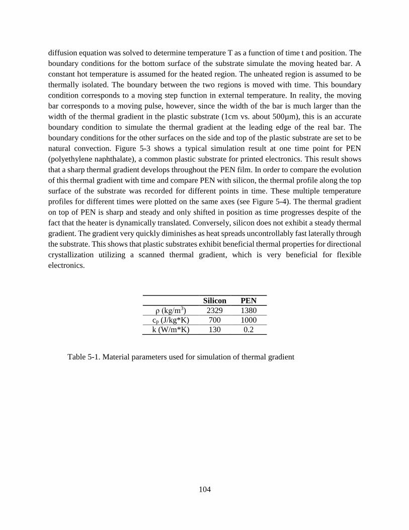
104
diffusion equation was solved to determine temperature T as a function of time t and position. The
boundary conditions for the bottom surface of the substrate simulate the moving heated bar. A
constant hot temperature is assumed for the heated region. The unheated region is assumed to be
thermally isolated. The boundary between the two regions is moved with time. This boundary
condition corresponds to a moving step function in external temperature. In reality, the moving
bar corresponds to a moving pulse, however, since the width of the bar is much larger than the
width of the thermal gradient in the plastic substrate (1cm vs. about 500µm), this is an accurate
boundary condition to simulate the thermal gradient at the leading edge of the real bar. The
boundary conditions for the other surfaces on the side and top of the plastic substrate are set to be
natural convection. Figure 5-3 shows a typical simulation result at one time point for PEN
(polyethylene naphthalate), a common plastic substrate for printed electronics. This result shows
that a sharp thermal gradient develops throughout the PEN film. In order to compare the evolution
of this thermal gradient with time and compare PEN with silicon, the thermal profile along the top
surface of the substrate was recorded for different points in time. These multiple temperature
profiles for different times were plotted on the same axes (see Figure 5-4). The thermal gradient
on top of PEN is sharp and steady and only shifted in position as time progresses despite of the
fact that the heater is dynamically translated. Conversely, silicon does not exhibit a steady thermal
gradient. The gradient very quickly diminishes as heat spreads uncontrollably fast laterally through
the substrate. This shows that plastic substrates exhibit beneficial thermal properties for directional
crystallization utilizing a scanned thermal gradient, which is very beneficial for flexible
electronics.
Silicon PEN
ρ (kg/m3) 2329 1380
cp (J/kg*K) 700 1000
k (W/m*K) 130 0.2
Table 5-1. Material parameters used for simulation of thermal gradient
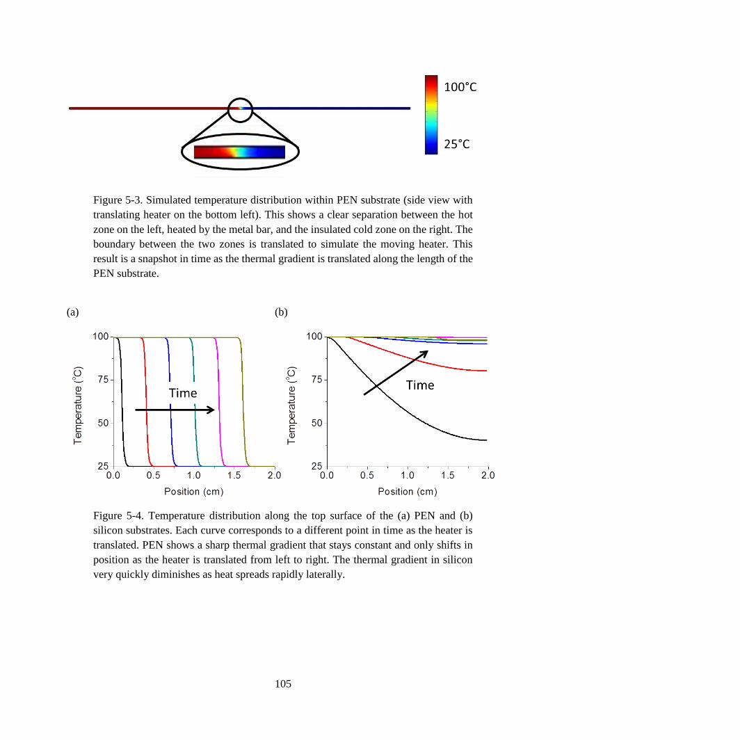
105
Figure 5-3. Simulated temperature distribution within PEN substrate (side view with
translating heater on the bottom left). This shows a clear separation between the hot
zone on the left, heated by the metal bar, and the insulated cold zone on the right. The
boundary between the two zones is translated to simulate the moving heater. This
result is a snapshot in time as the thermal gradient is translated along the length of the
PEN substrate.
(a) (b)
Figure 5-4. Temperature distribution along the top surface of the (a) PEN and (b)
silicon substrates. Each curve corresponds to a different point in time as the heater is
translated. PEN shows a sharp thermal gradient that stays constant and only shifts in
position as the heater is translated from left to right. The thermal gradient in silicon
very quickly diminishes as heat spreads rapidly laterally.

106
5.2.2 Device fabrication
Bottom-gate bottom-contact transistors were fabricated to study the crystallization mechanism and
electrical performance characteristics of the scanned thermal annealing technique demonstrated
here (see Figure 5-5 for device structure). Planarized PEN substrates were laser cut to a size of
9cm by 4cm of which an area of 4cm by 4cm was used for device fabrication. Silver gate electrodes
were inkjet-printed using CCI-300, a silver nanoparticle ink purchased from Cabot Corporation,
followed by sintering at 150⁰C for 30 minutes. The polymer gate dielectric lisicon® D207 was
deposited by spin coating at 3000RPM. The ink as received was diluted 1:1 by volume with 2-
Heptanone before spin coating. This resulted in an average film thickness of 330nm. The spun
layer was UV cross-linked for 10 minutes (λ=365nm, 3J/cm2). After a short UV ozone treatment
for 2 minutes, the source and drain electrodes were deposited by inkjet printing. The same CCI-
300 ink and sintering conditions were used as for the gate electrode. Before depositing the
semiconductor, a two-step surface treatment was applied.23 The source and drain electrodes and
the channel region were exposed to a forming gas RF plasma for 30 seconds at 40W. Within 5
minutes after the plasma cleaning step, lisicon® M001 was applied by drop casting. After spin
drying, the samples were rinsed with isopropyl alcohol and spin dried again. A state of the art
commercial organic semiconductor lisicon® S1200, which has been shown to hold great promise
for printed organic devices and circuits, was employed.19–21 Similar acene based organic
semiconductors have been studied extensively by John Anthony and co-workers.131,155,132 The
semiconductor was applied by spin coating. A high spin speed of 9000 RPM was chosen to realize
thin semiconductor layers, minimizing short channel effects. The semiconductor was crystallized
by uniform and by scanned annealing. Both were performed at the same temperature 100⁰C.
Uniform annealing was done on a standard hotplate for 1 minute. A custom built set-up was used
for scanned annealing (see Figure 5-1 for an illustration). The PEN substrate with devices on top
was pushed onto a heated aluminum bar. The bar was heated by a fire rod inserted into the bar and
the temperature was controlled by a thermocouple attached to the bar close to the area used for
annealing. The bar was then scanned at a speed of 1mm/s relative to the substrate. Both uniformly
annealed devices and devices with scanned annealing were subjected to a 5 minute post-anneal at
100⁰C on a hotplate to reduce the defect density and improve performance. Transistor
characteristics were measured using an Agilent 4156C semiconductor parameter analyzer in a
nitrogen atmosphere. All fabrication steps were performed in air.

107
Figure 5-5. Device structure of printed OTFTs.
5.2.3 Results and discussion
5.2.3.1 Device performance
Devices fabricated using scanned thermal annealing exhibit significantly improved electrical
performance when compared with devices fabricated using uniform annealing. Representative
transfer characteristics for short channel devices can be observed in Figure 5-6. Median transistor
parameters are summarized in Table 5-2. The greatest improvements can be observed for short
channel devices where the thermal gradient is scanned in parallel with the electrodes. Mobility is
increased by an order of magnitude from around 0.1cm2/V-s to over 1cm2/V-s. Off-state
characteristics are also improved in terms of subthreshold swing and turn-on voltage. On-off ratio
is good in all cases. This significant improvement is due to a greatly enhanced grain size. One can
clearly observe the difference between uniformly annealed samples, which exhibit randomly
oriented grains, and samples annealed by the scanned thermal gradient, which exhibit elongated
grains of much larger size (see Figure 5-7). Grains are aligned with the scanning direction
providing evidence of a successful separation of nucleation and growth during crystallization. This
is not only observed in areas away from devices but also in the channel region of transistors (see
Figure 5-8). This observation is especially clear for long channel devices.
In order to understand the crystallization mechanism better and to optimize performance, devices
with different channel lengths and scanning directions were fabricated. Two different scanning
directions were investigated: in parallel and perpendicular to the gate and source/drain electrodes
(see Figure 5-8 for illustration). A Welch’s t-test was performed on the experimentally obtained
saturation mobility distributions to identify statistically significant differences between conditions.
Statistically significant differences were found between uniformly annealed devices and devices
with scanned annealing in both directions. Significant differences were also found between the
108
two different scanning directions for long channel devices. Short and long channel devices were
also found to exhibit significantly different performance in the cases of both uniform annealing
and scanning parallel to the electrodes. However, for short channel devices, no statistically
significant differences were found between the scanning directions. For scanning perpendicular to
the electrodes, no statistically significant differences were found between short and long channel
devices either. These effects can be explained by considering both crystallization effects and the
effect of contact resistance.
(a) (b)
Figure 5-6. Representative transfer characteristics of short channel devices (25µm
channel length and 830µm channel width) crystallized by (a) uniform heating and (b)
scanned thermal annealing (scanning direction in parallel with electrodes). The
switching performance is significantly improved by scanned annealing both in the on-
and off-state.
109
L
[µm]
Anneal Linear
mobility
[cm2/V-s]
Saturation
mobility
[cm2/V-s]
On-off
ratio
Subthreshol
d swing
[V/dec]
Von
[V]
30 Uniform 0.086 0.099 1.0*105 1.27 7.50
30 Scanned
perpendicular
0.90 1.08 2.4*107 0.49 6.63
30 Scanned
parallel
0.98 1.27 2.9*106 0.46 5.25
220 Uniform 0.26 0.32 1.8*104 1.77 7.00
220 Scanned
perpendicular
0.91 1.09 2.0*104 0.55 0.50
220 Scanned
parallel
1.34 1.52 1.1*106 0.52 2.00
Table 5-2. Median values of transistor characteristics for different channel lengths and
annealing methods.
(a) (b)
Figure 5-7. Polarized optical microscope images showing crystallization away from
transistors. (a) Uniform annealing. Randomly oriented small grains. (b) Scanned
thermal annealing. Arrow indicates scanning direction. Grains are clearly enlarged and
aligned with the scanning direction as expected for the successful separation of
nucleation and growth.
50µm
110
Figure 5-8. Polarized optical micrographs of grain structure for different annealing
conditions. Black arrow indicates scanning directions. (a)&(b) Uniform annealing.
Grains are randomly oriented and small. (c)-(e) Scanned thermal annealing
perpendicular to electrodes. Grains are elongated and aligned with the scanning
direction. Small secondary grains impinge on large primary grains close to the second
electrode. This is most prevalent for long channel devices. (f)-(h) Scanned thermal
annealing in parallel with electrodes. Grains are again aligned with the scanning
direction and have the largest size of all the tested conditions. No impingement on
secondary grains is observed.
111
5.2.3.2 Effect of channel length
Both uniformly annealed devices and devices with scanned annealing parallel to the electrodes
exhibit increased performance for longer channels compared with shorter channel devices
annealed under the same conditions. One reason is the preferred nucleation of the semiconductor
on the electrodes. This leads to smaller grains on and close to the electrodes. This disruption of the
crystallization will impact short channel devices more severely because the region close to the
electrodes makes up a larger portion of the channel. Secondly, short channel devices are limited
by contact resistance due to a contact barrier. This has been minimized with a surface treatment,
however, has not been eliminated completely. In the case of short channel devices, the mean
saturation mobility is about 30% higher than the mean linear mobility due to the larger effect of
contact resistance in the linear regime. For long channel devices, this difference is reduced to about
10% as one would expect due to the larger influence of channel resistance compared with contact
resistance. Both effects combined lead to the limited performance of short channel devices.
5.2.3.3 Effect of scanning direction
Devices fabricated using scanning perpendicular to the electrodes generally exhibit lower
performance than devices fabricated by scanning parallel to the electrodes. The worst case devices
and the variability of performance tend to be worse for devices fabricated using scanning
perpendicular to the electrodes (see Figure 5-9 for boxplot of saturation mobility). The difference
in mean saturation mobility between scanning directions is more pronounced and only statistically
significant for long channel devices. Long channel devices fabricated by perpendicular scanning
are limited in performance despite the smaller effect of contact resistance compared with shorter
channel devices. Therefore no significant effect of channel length can be observed for
perpendicular scanning. To understand this effect, we may consider the details of the
crystallization mechanism. This is schematically illustrated in Figure 5-10. For perpendicular
scanning, the thermal gradient will initially approach one of the source/ drain electrodes (the upper
electrode in Figure 5-8). Nucleation will occur on this electrode and then grains will grow into the
channel without further nucleation, leading to elongated grains. As the thermal gradient
approaches the second (bottom) electrode, further nucleation will occur on this electrode. These
secondary grains can grow back into the channel impinging on the elongated primary grains
growing from the primary (top) electrode. This creates significant disorder and smaller grains close
to the second electrode, which will limit device performance, and can be observed clearly for the
long channel devices in Figure 5-8 (d) and (e) and is illustrated in Figure 5-10. This mechanism
does not exist for devices fabricated using scanning parallel to the electrodes. In these devices,
grains grow from both electrodes simultaneously and only impinge once at the center of the
channel (see both Figure 5-10 and Figure 5-8 (h)). This explains the improved performance of
devices where the thermal gradient is scanned in parallel with the electrodes. Further, in the case
of devices fabricated using scanning perpendicular to the electrodes, short channel devices are less

112
limited by primary grains impinging on secondary grains since both primary and secondary grains
can bridge shorter channels more easily as the size of the secondary grains is comparable to the
channel length. This effect is offset by the effect of contact resistance. Considering these effects
together, both the crystallization and contact resistance effects then result in no net difference in
performance between short and long channel devices when the thermal gradient is scanned
perpendicular to the electrodes. However, even with this slightly lessened improvement in devices
fabricated by scanning perpendicular to the electrodes, the scanning technique clearly gives
significant improvement in performance across all device geometries relative to uniform
annealing. Indeed, scanning perpendicular to the channel results in devices with more uniform
device characteristics across all channel lengths, which is beneficial for the design of realistic
circuits. The significant performance improvement across the board under these conditions is very
attractive, as a result.
Figure 5-9. Boxplot comparing performance statistics of different annealing
conditions (uniform annealing, scanning perpendicular and scanning parallel to
electrodes) and channel lengths.
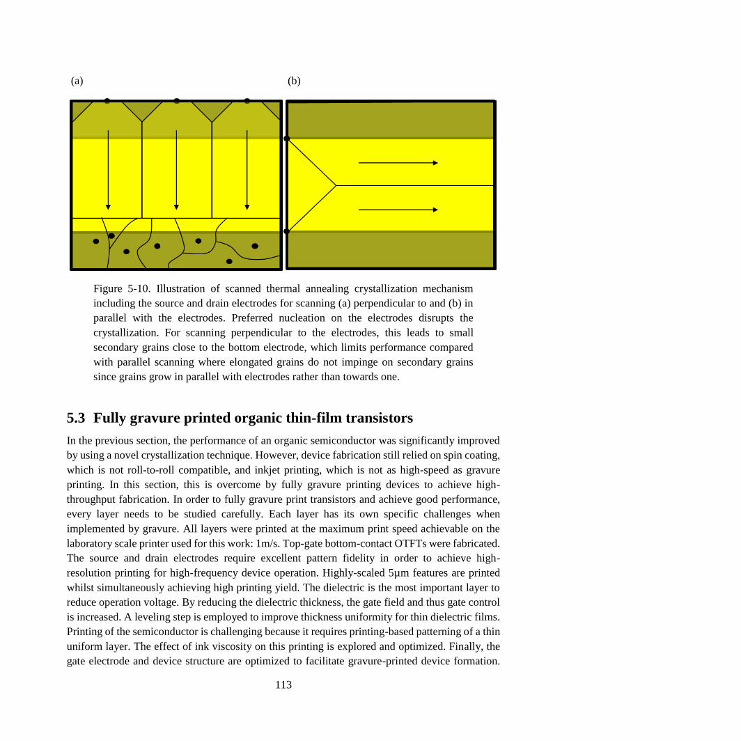
113
(a) (b)
Figure 5-10. Illustration of scanned thermal annealing crystallization mechanism
including the source and drain electrodes for scanning (a) perpendicular to and (b) in
parallel with the electrodes. Preferred nucleation on the electrodes disrupts the
crystallization. For scanning perpendicular to the electrodes, this leads to small
secondary grains close to the bottom electrode, which limits performance compared
with parallel scanning where elongated grains do not impinge on secondary grains
since grains grow in parallel with electrodes rather than towards one.
5.3 Fully gravure printed organic thin-film transistors
In the previous section, the performance of an organic semiconductor was significantly improved
by using a novel crystallization technique. However, device fabrication still relied on spin coating,
which is not roll-to-roll compatible, and inkjet printing, which is not as high-speed as gravure
printing. In this section, this is overcome by fully gravure printing devices to achieve high-
throughput fabrication. In order to fully gravure print transistors and achieve good performance,
every layer needs to be studied carefully. Each layer has its own specific challenges when
implemented by gravure. All layers were printed at the maximum print speed achievable on the
laboratory scale printer used for this work: 1m/s. Top-gate bottom-contact OTFTs were fabricated.
The source and drain electrodes require excellent pattern fidelity in order to achieve high-
resolution printing for high-frequency device operation. Highly-scaled 5µm features are printed
whilst simultaneously achieving high printing yield. The dielectric is the most important layer to
reduce operation voltage. By reducing the dielectric thickness, the gate field and thus gate control
is increased. A leveling step is employed to improve thickness uniformity for thin dielectric films.
Printing of the semiconductor is challenging because it requires printing-based patterning of a thin
uniform layer. The effect of ink viscosity on this printing is explored and optimized. Finally, the
gate electrode and device structure are optimized to facilitate gravure-printed device formation.

114
For gravure printing, alignment accuracy currently lags behind feature size, which means
alignment of the gate electrode to the source and drain electrodes is very challenging. Alignment
accuracy is reduced both by tool limitations, which will be addressed in future generation tools, as
well as by more fundamental issues with flexible substrates such as stretching or dimensional
changes during heating steps. Addressing these challenges in the future would be an important step
forward for the gravure printing of multi-layer devices. In the meantime, a fully overlapped gate
structure is employed with a large gate electrode. Due to the large size of the gate relative to the
channel and source-drain dimensions, the structure becomes misalignment tolerant.27 Thus, gate
pattern size is not very critical. The main challenge with the gate is to choose an ink that
sufficiently wets the dielectric and whose solvent does not interact with the dielectric. See Figure
5-11 for the device structure and the fabrication process.
(a) (b) (c) (d)
Figure 5-11. Overview of fabrication process and device structure. (a) Highly-scaled
silver electrodes are gravure printed on cleaned PEN plastic substrates. (b) After a self-
assembled monolayer treatment, the polymer semiconductor is patterned using
gravure printing. (c) The dielectric is blanket printed using gravure. (d) The silver gate
electrode is patterned by gravure printing. All printing steps are performed at 1m/s in
air.
5.3.1 Device fabrication
5.3.1.1 Source and drain printing
Downscaling of the source and drain electrodes and their spacing is crucial to achieve high-
performance TFT operation. In order to achieve good AC performance, the fully overlapped gate
architecture requires not only a highly-scaled channel length but also highly-scaled electrodes to
minimize overlap capacitance. Electrodes are printed whose width is on the same order as the
channel length. The previous chapters showed how high-resolution features can be printed at high
print speeds using gravure. Again, electrodes were printed onto planarized polyethylene
naphthalate (PEN) substrates provided by DuPont Teijin Films after a 30 seconds, 50W air plasma
treatment. The ink for the source and drain electrodes was again the silver nanoparticle ink (NPS)
purchased from Harima Chemicals Group and its viscosity was adjusted by dilution with its solvent
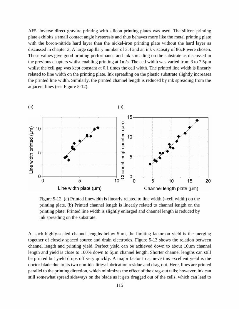
115
AF5. Inverse direct gravure printing with silicon printing plates was used. The silicon printing
plate exhibits a small contact angle hysteresis and thus behaves more like the metal printing plate
with the boron-nitride hard layer than the nickel-iron printing plate without the hard layer as
discussed in chapter 3. A large capillary number of 3.4 and an ink viscosity of 86cP were chosen.
These values give good printing performance and ink spreading on the substrate as discussed in
the previous chapters whilst enabling printing at 1m/s. The cell width was varied from 3 to 7.5µm
whilst the cell gap was kept constant at 0.1 times the cell width. The printed line width is linearly
related to line width on the printing plate. Ink spreading on the plastic substrate slightly increases
the printed line width. Similarly, the printed channel length is reduced by ink spreading from the
adjacent lines (see Figure 5-12).
(a) (b)
Figure 5-12. (a) Printed linewidth is linearly related to line width (=cell width) on the
printing plate. (b) Printed channel length is linearly related to channel length on the
printing plate. Printed line width is slightly enlarged and channel length is reduced by
ink spreading on the substrate.
At such highly-scaled channel lengths below 5µm, the limiting factor on yield is the merging
together of closely spaced source and drain electrodes. Figure 5-13 shows the relation between
channel length and printing yield. Perfect yield can be achieved down to about 10µm channel
length and yield is close to 100% down to 5µm channel length. Shorter channel lengths can still
be printed but yield drops off very quickly. A major factor to achieve this excellent yield is the
doctor blade due to its two non-idealities: lubrication residue and drag-out. Here, lines are printed
parallel to the printing direction, which minimizes the effect of the drag-out tails; however, ink can
still somewhat spread sideways on the blade as it gets dragged out of the cells, which can lead to

116
the merging of adjacent lines. Ideally, both wiping non-idealities occur uniformly across the print.
However, doctor blades typically have local defects whose density gets worse during printing due
to doctor blade wear. In the worst case, these defects can cause the printing of large streaks that
run throughout the print. Even without such catastrophic streaks, doctor blade defects and wear
affect yield dramatically for highly-scaled features. Figure 5-14 shows how yield changes
throughout a print for different doctor blade tip thicknesses (see Figure 5-15 for cross-sectional
micrographs of different blade tips). Doctor blades were used as supplied by Max Daetwyler
Corporation. A thin 60µm tip shows dramatic degradation in yield as the print progresses because
it is very susceptible to wear (see Figure 5-16 for optical micrographs of pattern degradation). A
75µm tip is far more robust. Yield even increases slightly after the beginning of the print, possibly
because initial defects are polished away. However, increasing the tip thickness too much leads to
decreased print quality and yield as evidenced by the 95µm tip. Larger tips develop a smaller
pressure at the tip leading to increased lubrication residue and allow more time for drag-out to
occur. A 75µm tip was thus used to fabricate devices.
Figure 5-13. Printing yield of source-drain patterns is close to 100% for channel
lengths above 5µm. Below 5µm, the number of merged lines increases significantly.
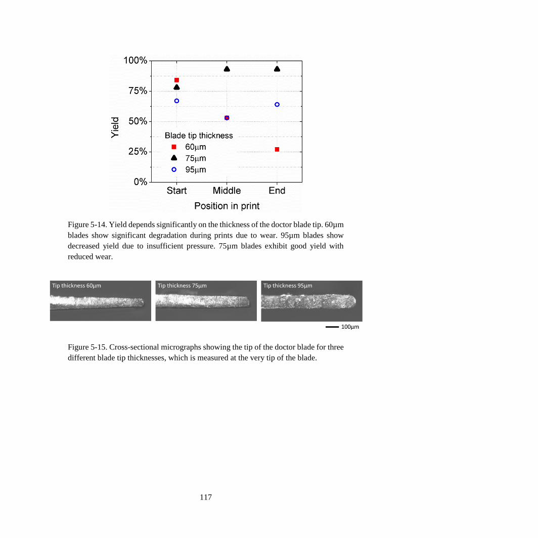
117
Figure 5-14. Yield depends significantly on the thickness of the doctor blade tip. 60µm
blades show significant degradation during prints due to wear. 95µm blades show
decreased yield due to insufficient pressure. 75µm blades exhibit good yield with
reduced wear.
Figure 5-15. Cross-sectional micrographs showing the tip of the doctor blade for three
different blade tip thicknesses, which is measured at the very tip of the blade.
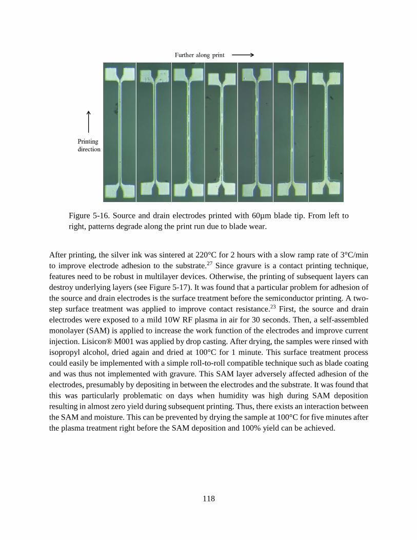
118
Figure 5-16. Source and drain electrodes printed with 60µm blade tip. From left to
right, patterns degrade along the print run due to blade wear.
After printing, the silver ink was sintered at 220°C for 2 hours with a slow ramp rate of 3°C/min
to improve electrode adhesion to the substrate.27 Since gravure is a contact printing technique,
features need to be robust in multilayer devices. Otherwise, the printing of subsequent layers can
destroy underlying layers (see Figure 5-17). It was found that a particular problem for adhesion of
the source and drain electrodes is the surface treatment before the semiconductor printing. A two-
step surface treatment was applied to improve contact resistance.23 First, the source and drain
electrodes were exposed to a mild 10W RF plasma in air for 30 seconds. Then, a self-assembled
monolayer (SAM) is applied to increase the work function of the electrodes and improve current
injection. Lisicon® M001 was applied by drop casting. After drying, the samples were rinsed with
isopropyl alcohol, dried again and dried at 100°C for 1 minute. This surface treatment process
could easily be implemented with a simple roll-to-roll compatible technique such as blade coating
and was thus not implemented with gravure. This SAM layer adversely affected adhesion of the
electrodes, presumably by depositing in between the electrodes and the substrate. It was found that
this was particularly problematic on days when humidity was high during SAM deposition
resulting in almost zero yield during subsequent printing. Thus, there exists an interaction between
the SAM and moisture. This can be prevented by drying the sample at 100°C for five minutes after
the plasma treatment right before the SAM deposition and 100% yield can be achieved.

119
Figure 5-17. Silver rectangles on PEN after SAM treatment without drying and
subsequent semiconductor printing. One can clearly observe regions of the rectangles
that have been destroyed during the semiconductor printing.
5.3.1.2 Semiconductor printing
The semiconductor material is crucial in determining the performance of a transistor. Here,
lisicon® SP400 is employed. This material as well as the surface treatment and the dielectric were
provided by EMD Performance Materials Corp. (an affiliate of Merck KGaA, Darmstadt,
Germany). This p-type semiconductor is a high-performance amorphous polymer. The amorphous
nature of the material reduces processing complexity and variability because there is no need for
a crystallization step, and device to device uniformity is improved due to the elimination of grain
boundary-induced variation as a performance-determining parameter. In addition, patterning and
control over the rheology is significantly improved by the fact that lisicon® SP400 is a polymer
rather than a small molecule. Patterning of the semiconductor layer is, in practice, imperative to
realize functional organic semiconductor-based circuits. When the semiconductor is patterned,
leakage paths are removed that would otherwise lead to excessive device off-current and cross-
talk between neighboring devices. The pattern dimensions for the semiconductor are much larger
than for the source and drain electrodes, typically on the order of tens to hundreds of micrometers.
Thus, they can be printed using conventional direct gravure with a metal roll fabricated by
electromechanical engraving. The roll was purchased from RotaDyne. However, patterning of the
semiconductor is more challenging because low viscosity inks are used to achieve thin films. The
use of thin films is desirable to obtain good device electrostatic integrity, resulting in improved
off-state behavior. Lowering the polymer concentration in the ink decreases both dry film
thickness and ink viscosity. The ink was diluted with its two co-solvents mesitylene and 1-methyl
naphthalene. Figure 5-18 shows how the pattern fidelity changes with different ink viscosities. As
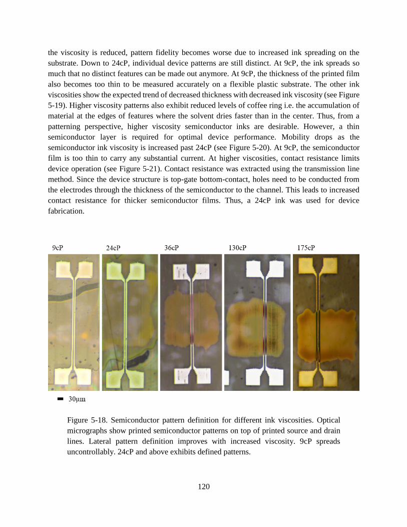
120
the viscosity is reduced, pattern fidelity becomes worse due to increased ink spreading on the
substrate. Down to 24cP, individual device patterns are still distinct. At 9cP, the ink spreads so
much that no distinct features can be made out anymore. At 9cP, the thickness of the printed film
also becomes too thin to be measured accurately on a flexible plastic substrate. The other ink
viscosities show the expected trend of decreased thickness with decreased ink viscosity (see Figure
5-19). Higher viscosity patterns also exhibit reduced levels of coffee ring i.e. the accumulation of
material at the edges of features where the solvent dries faster than in the center. Thus, from a
patterning perspective, higher viscosity semiconductor inks are desirable. However, a thin
semiconductor layer is required for optimal device performance. Mobility drops as the
semiconductor ink viscosity is increased past 24cP (see Figure 5-20). At 9cP, the semiconductor
film is too thin to carry any substantial current. At higher viscosities, contact resistance limits
device operation (see Figure 5-21). Contact resistance was extracted using the transmission line
method. Since the device structure is top-gate bottom-contact, holes need to be conducted from
the electrodes through the thickness of the semiconductor to the channel. This leads to increased
contact resistance for thicker semiconductor films. Thus, a 24cP ink was used for device
fabrication.
Figure 5-18. Semiconductor pattern definition for different ink viscosities. Optical
micrographs show printed semiconductor patterns on top of printed source and drain
lines. Lateral pattern definition improves with increased viscosity. 9cP spreads
uncontrollably. 24cP and above exhibits defined patterns.
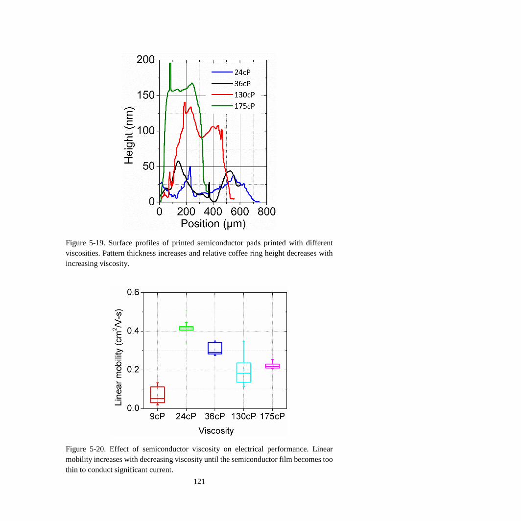
121
Figure 5-19. Surface profiles of printed semiconductor pads printed with different
viscosities. Pattern thickness increases and relative coffee ring height decreases with
increasing viscosity.
Figure 5-20. Effect of semiconductor viscosity on electrical performance. Linear
mobility increases with decreasing viscosity until the semiconductor film becomes too
thin to conduct significant current.

122
Figure 5-21. Thinner semiconductor films printed with lower viscosity inks lead to
improved contact resistance in a top-gate bottom-contact device structure where
current is conducted through the semiconductor thickness.
5.3.1.3 Dielectric scaling
The gate dielectric is crucial in ensuring good electrostatic control over the channel. Here, lisicon®
D320 is used, a polymer dielectric provided by EMD Performance Materials Corp., which has
been designed to match with the semiconductor lisicon® SP400. The semiconductor-dielectric
interface is optimized to ensure a low trap concentration, enabling the realization of devices with
high mobility and low subthreshold swing. In addition, the semiconductor is compatible with the
dielectric solvent (decane). It is also important for the dielectric to have a high enough surface
energy such that the subsequent gate ink does not dewet, which is a problem for fluorinated gate
dielectrics. The dielectric was blanket printed using a roll purchased from IGT Testing Systems
(402.101, 45µm cell depth). In order to achieve low-voltage operation, the gate dielectric needs to
be scaled down in thickness to increase the gate field and improve gate control over the channel.
Here, a number of different dielectric thicknesses were studied. Thickness was varied by dilution
of the dielectric ink. As the dielectric thickness is scaled, off-state performance improves
significantly (see Figure 5-22). For a 120nm thick dielectric, the magnitude of the threshold
voltage decreases to approximately -1V and swing drops below 500mV/decade. In order to achieve
such thickness scaling, a very uniform dielectric needs to be printed. Gravure printing often leads
to non-uniform films due to fluid instabilities as well as the discrete nature of the gravure cells that
requires ink to spread in between cells.130 Here, a leveling step in a solvent atmosphere is employed
before drying at 100°C for 5 minutes to improve the uniformity of the dielectric thickness and
dielectric yield significantly (see Figure 5-23). However, dielectric yield still needs to be improved
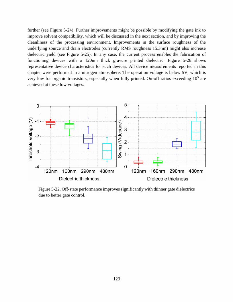
123
further (see Figure 5-24). Further improvements might be possible by modifying the gate ink to
improve solvent compatibility, which will be discussed in the next section, and by improving the
cleanliness of the processing environment. Improvements in the surface roughness of the
underlying source and drain electrodes (currently RMS roughness 15.3nm) might also increase
dielectric yield (see Figure 5-25). In any case, the current process enables the fabrication of
functioning devices with a 120nm thick gravure printed dielectric. Figure 5-26 shows
representative device characteristics for such devices. All device measurements reported in this
chapter were performed in a nitrogen atmosphere. The operation voltage is below 5V, which is
very low for organic transistors, especially when fully printed. On-off ratios exceeding 105 are
achieved at these low voltages.
Figure 5-22. Off-state performance improves significantly with thinner gate dielectrics
due to better gate control.
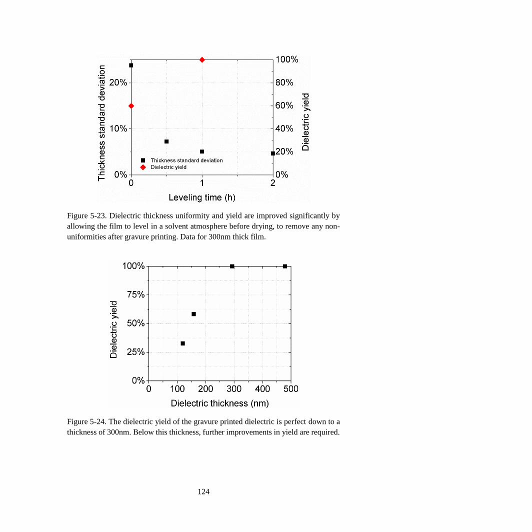
124
Figure 5-23. Dielectric thickness uniformity and yield are improved significantly by
allowing the film to level in a solvent atmosphere before drying, to remove any non-
uniformities after gravure printing. Data for 300nm thick film.
Figure 5-24. The dielectric yield of the gravure printed dielectric is perfect down to a
thickness of 300nm. Below this thickness, further improvements in yield are required.

125
Figure 5-25. Height profile of source and drain lines. The average RMS surface
roughness is 15.3nm. Improvements in source and drain surface roughness might
improve dielectric yield.
Figure 5-26. Representative transfer and output characteristics exhibiting low-voltage
operation with excellent off-state performance.
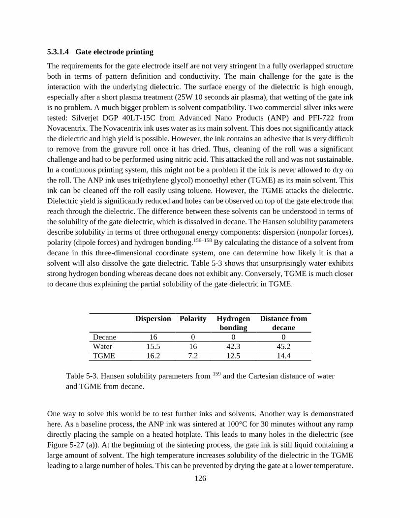
126
5.3.1.4 Gate electrode printing
The requirements for the gate electrode itself are not very stringent in a fully overlapped structure
both in terms of pattern definition and conductivity. The main challenge for the gate is the
interaction with the underlying dielectric. The surface energy of the dielectric is high enough,
especially after a short plasma treatment (25W 10 seconds air plasma), that wetting of the gate ink
is no problem. A much bigger problem is solvent compatibility. Two commercial silver inks were
tested: Silverjet DGP 40LT-15C from Advanced Nano Products (ANP) and PFI-722 from
Novacentrix. The Novacentrix ink uses water as its main solvent. This does not significantly attack
the dielectric and high yield is possible. However, the ink contains an adhesive that is very difficult
to remove from the gravure roll once it has dried. Thus, cleaning of the roll was a significant
challenge and had to be performed using nitric acid. This attacked the roll and was not sustainable.
In a continuous printing system, this might not be a problem if the ink is never allowed to dry on
the roll. The ANP ink uses tri(ethylene glycol) monoethyl ether (TGME) as its main solvent. This
ink can be cleaned off the roll easily using toluene. However, the TGME attacks the dielectric.
Dielectric yield is significantly reduced and holes can be observed on top of the gate electrode that
reach through the dielectric. The difference between these solvents can be understood in terms of
the solubility of the gate dielectric, which is dissolved in decane. The Hansen solubility parameters
describe solubility in terms of three orthogonal energy components: dispersion (nonpolar forces),
polarity (dipole forces) and hydrogen bonding.156–158 By calculating the distance of a solvent from
decane in this three-dimensional coordinate system, one can determine how likely it is that a
solvent will also dissolve the gate dielectric. Table 5-3 shows that unsurprisingly water exhibits
strong hydrogen bonding whereas decane does not exhibit any. Conversely, TGME is much closer
to decane thus explaining the partial solubility of the gate dielectric in TGME.
Dispersion Polarity Hydrogen
bonding
Distance from
decane
Decane 16 0 0 0
Water 15.5 16 42.3 45.2
TGME 16.2 7.2 12.5 14.4
Table 5-3. Hansen solubility parameters from 159 and the Cartesian distance of water
and TGME from decane.
One way to solve this would be to test further inks and solvents. Another way is demonstrated
here. As a baseline process, the ANP ink was sintered at 100°C for 30 minutes without any ramp
directly placing the sample on a heated hotplate. This leads to many holes in the dielectric (see
Figure 5-27 (a)). At the beginning of the sintering process, the gate ink is still liquid containing a
large amount of solvent. The high temperature increases solubility of the dielectric in the TGME
leading to a large number of holes. This can be prevented by drying the gate at a lower temperature.

127
Drying at 30°C for 15 minutes under vacuum results in a significant reduction in hole density (see
Figure 5-27 (b)). The vacuum aids with the removal of the solvent and enables lines to be
conductive even at such low temperatures. Further heating of the gate at 100°C after drying
improves conductivity but does not result in the creation of holes in the dielectric further
confirming that the holes are due to solvent interaction. The vacuum step can be replaced by
sintering in air using a very slow ramp of 2°C per minute to ramp up to 100°C. With this process,
perfect yield can be achieved down to a dielectric thickness of 300nm (see Figure 5-24). Further
improvements are needed for thinner dielectrics.
(a) (b) (c)
Figure 5-27. ANP gate on top of D320 gate dielectric after sintering. (a) Sintering at
100°C for 30 minutes without ramp resulting in large number of holes in dielectric
(black dots). (b) Sintering at 30°C for 15 minutes in vacuum significantly improves
the hole density. (c) Further heating at 100°C for 10 minutes after initial drying at
30°C does not result in the creation of holes.
5.3.2 Device characterization
5.3.2.1 Comparison with small molecule semiconductor
One reason for choosing a polymer semiconductor is its better printability compared with small
molecule semiconductors. This facilitates the printing of patterned semiconductor pads. In
addition, the polymer used here is amorphous, which allows for achievement of very good device-
to-device uniformity. In contrast, the performance of small molecule polycrystalline organic
semiconductors depends very strongly on the grain size and the location of grain boundaries. Due
to the random nature of the crystallization process, devices with small molecule semiconductors
tend to be more variable than devices with amorphous semiconductors. Furthermore,
polycrystalline semiconductors have larger surface roughness due to grain boundaries that can be
problematic for the yield of the dielectric deposited on top. Here, we compare our amorphous
polymer TFTs with devices fabricated using a state-of-the-art polycrystalline small molecule
semiconductor (Lisicon® S1200) supplied by EMD Performance Materials Corp. These small
molecule devices were fabricated with a very similar process except the small molecule
semiconductor was polycrystalline and not patterned, the dielectric was 200nm thick and the gate
was patterned by inkjet printing.27 Figure 5-28 shows the difference in electrical performance
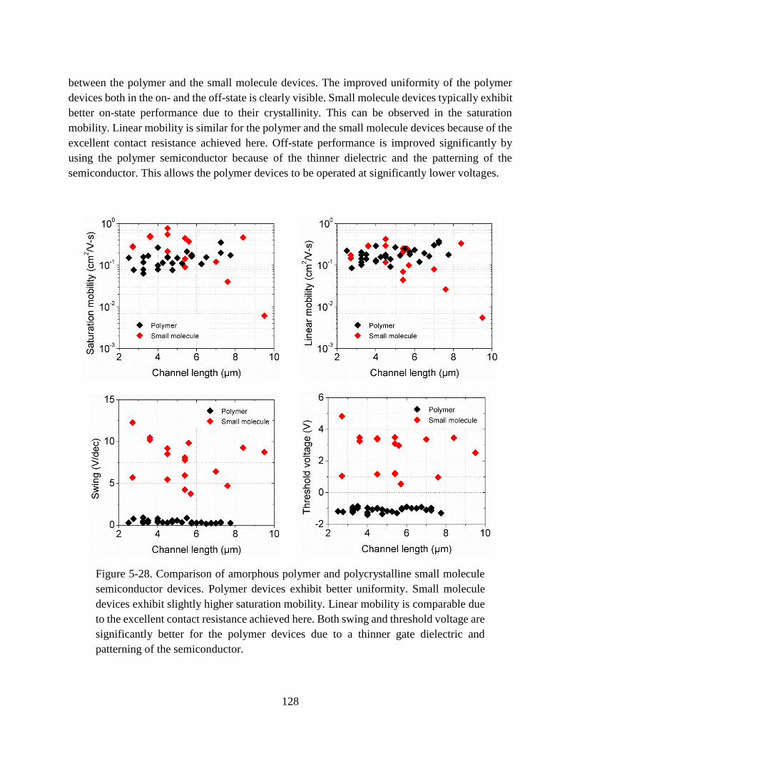
128
between the polymer and the small molecule devices. The improved uniformity of the polymer
devices both in the on- and the off-state is clearly visible. Small molecule devices typically exhibit
better on-state performance due to their crystallinity. This can be observed in the saturation
mobility. Linear mobility is similar for the polymer and the small molecule devices because of the
excellent contact resistance achieved here. Off-state performance is improved significantly by
using the polymer semiconductor because of the thinner dielectric and the patterning of the
semiconductor. This allows the polymer devices to be operated at significantly lower voltages.
Figure 5-28. Comparison of amorphous polymer and polycrystalline small molecule
semiconductor devices. Polymer devices exhibit better uniformity. Small molecule
devices exhibit slightly higher saturation mobility. Linear mobility is comparable due
to the excellent contact resistance achieved here. Both swing and threshold voltage are
significantly better for the polymer devices due to a thinner gate dielectric and
patterning of the semiconductor.
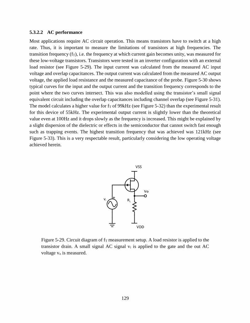
129
5.3.2.2 AC performance
Most applications require AC circuit operation. This means transistors have to switch at a high
rate. Thus, it is important to measure the limitations of transistors at high frequencies. The
transition frequency (fT), i.e. the frequency at which current gain becomes unity, was measured for
these low-voltage transistors. Transistors were tested in an inverter configuration with an external
load resistor (see Figure 5-29). The input current was calculated from the measured AC input
voltage and overlap capacitances. The output current was calculated from the measured AC output
voltage, the applied load resistance and the measured capacitance of the probe. Figure 5-30 shows
typical curves for the input and the output current and the transition frequency corresponds to the
point where the two curves intersect. This was also modelled using the transistor’s small signal
equivalent circuit including the overlap capacitances including channel overlap (see Figure 5-31).
The model calculates a higher value for fT of 99kHz (see Figure 5-32) than the experimental result
for this device of 55kHz. The experimental output current is slightly lower than the theoretical
value even at 100Hz and it drops slowly as the frequency is increased. This might be explained by
a slight dispersion of the dielectric or effects in the semiconductor that cannot switch fast enough
such as trapping events. The highest transition frequency that was achieved was 121kHz (see
Figure 5-33). This is a very respectable result, particularly considering the low operating voltage
achieved herein.
Figure 5-29. Circuit diagram of fT measurement setup. A load resistor is applied to the
transistor drain. A small signal AC signal vi is applied to the gate and the out AC
voltage vo is measured.
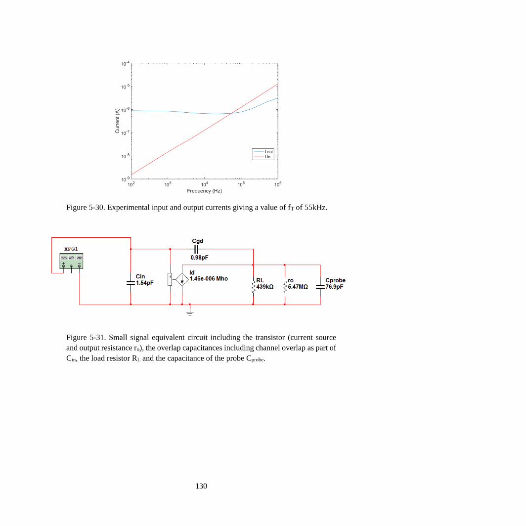
130
Figure 5-30. Experimental input and output currents giving a value of fT of 55kHz.
Figure 5-31. Small signal equivalent circuit including the transistor (current source
and output resistance ro), the overlap capacitances including channel overlap as part of
Cin, the load resistor RL and the capacitance of the probe Cprobe.
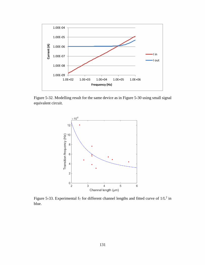
131
Figure 5-32. Modelling result for the same device as in Figure 5-30 using small signal
equivalent circuit.
Figure 5-33. Experimental fT for different channel lengths and fitted curve of 1/L2 in
blue.
1.00E-09
1.00E-08
1.00E-07
1.00E-06
1.00E-05
1.00E-04
1.0E+02 1.0E+03 1.0E+04 1.0E+05 1.0E+06
Cu
rre
nt
(A)
Frequency (Hz)
I in
I out
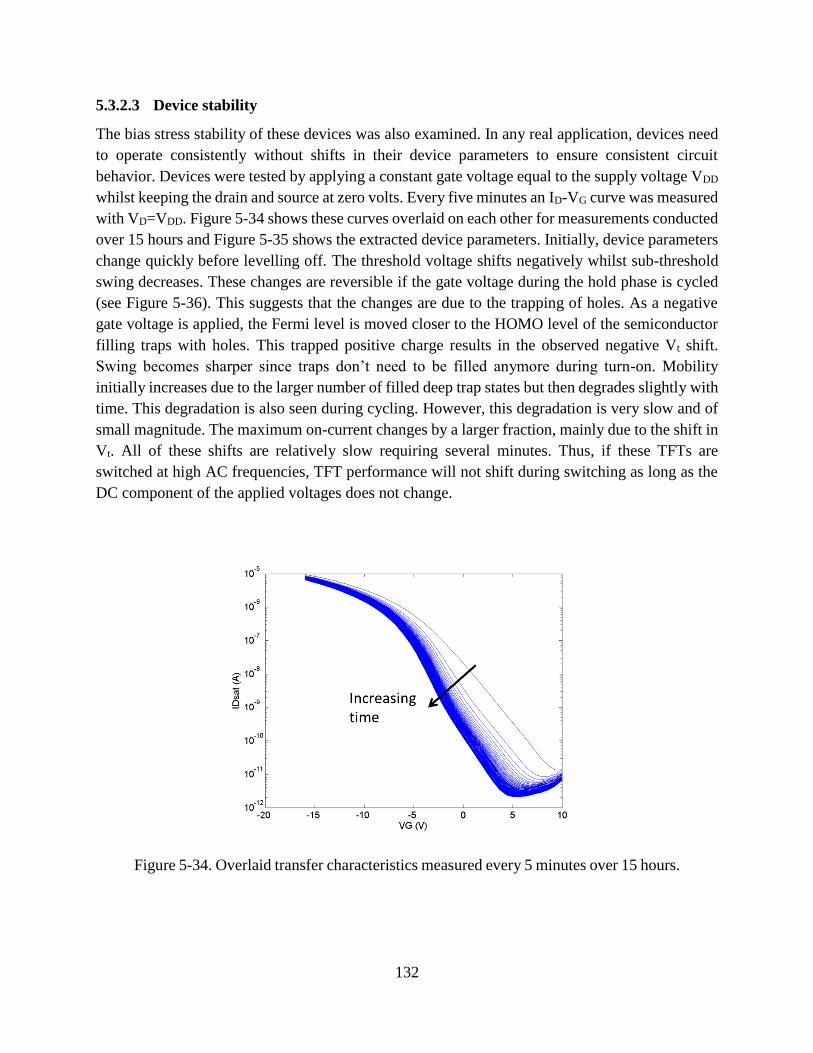
132
5.3.2.3 Device stability
The bias stress stability of these devices was also examined. In any real application, devices need
to operate consistently without shifts in their device parameters to ensure consistent circuit
behavior. Devices were tested by applying a constant gate voltage equal to the supply voltage VDD
whilst keeping the drain and source at zero volts. Every five minutes an ID-VG curve was measured
with VD=VDD. Figure 5-34 shows these curves overlaid on each other for measurements conducted
over 15 hours and Figure 5-35 shows the extracted device parameters. Initially, device parameters
change quickly before levelling off. The threshold voltage shifts negatively whilst sub-threshold
swing decreases. These changes are reversible if the gate voltage during the hold phase is cycled
(see Figure 5-36). This suggests that the changes are due to the trapping of holes. As a negative
gate voltage is applied, the Fermi level is moved closer to the HOMO level of the semiconductor
filling traps with holes. This trapped positive charge results in the observed negative Vt shift.
Swing becomes sharper since traps don’t need to be filled anymore during turn-on. Mobility
initially increases due to the larger number of filled deep trap states but then degrades slightly with
time. This degradation is also seen during cycling. However, this degradation is very slow and of
small magnitude. The maximum on-current changes by a larger fraction, mainly due to the shift in
Vt. All of these shifts are relatively slow requiring several minutes. Thus, if these TFTs are
switched at high AC frequencies, TFT performance will not shift during switching as long as the
DC component of the applied voltages does not change.
Figure 5-34. Overlaid transfer characteristics measured every 5 minutes over 15 hours.

133
Figure 5-35. Transistor characteristics extracted from the transfer characteristics in
Figure 5-34.

134
Figure 5-36. Cycling of hold voltage in between ID-VG measurements showing
reversibility of behavior with the exception of mobility.
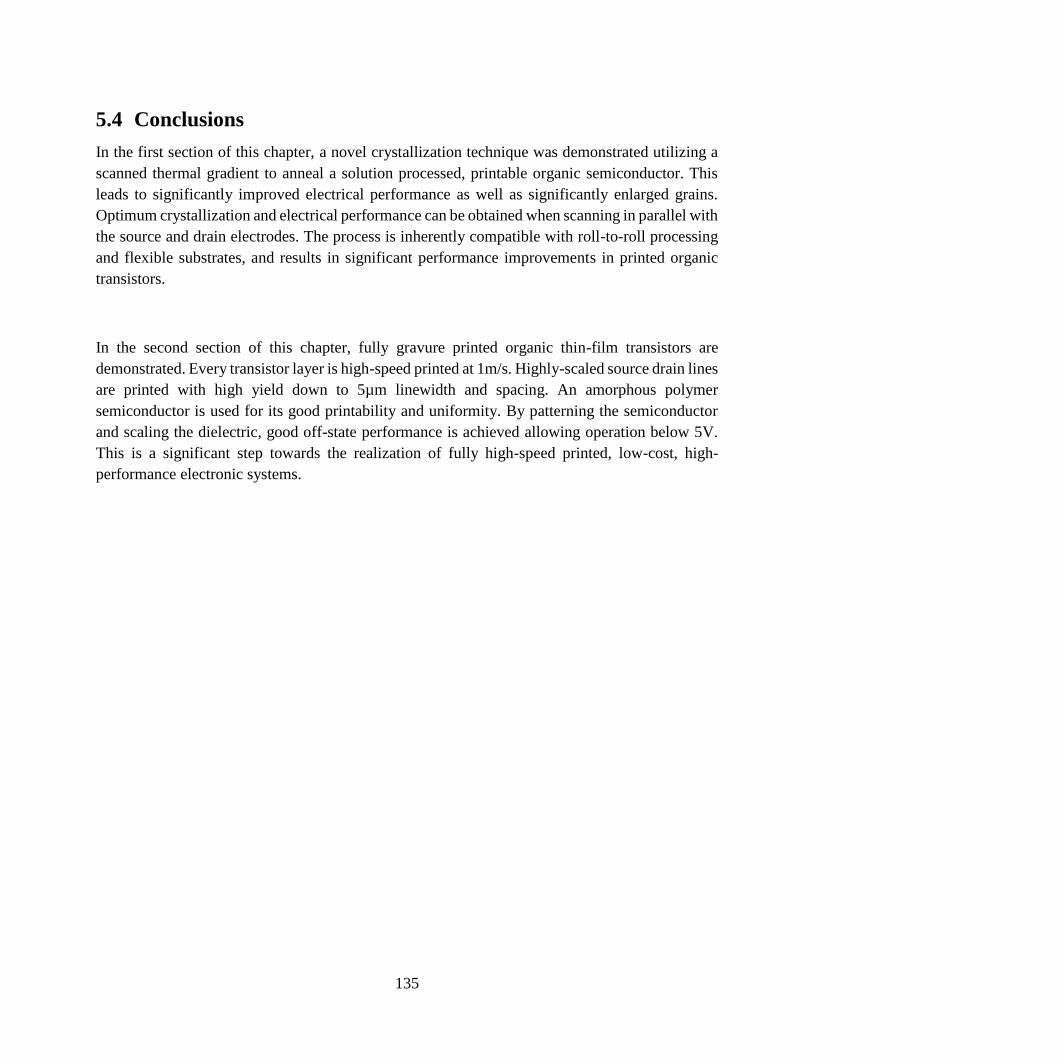
135
5.4 Conclusions
In the first section of this chapter, a novel crystallization technique was demonstrated utilizing a
scanned thermal gradient to anneal a solution processed, printable organic semiconductor. This
leads to significantly improved electrical performance as well as significantly enlarged grains.
Optimum crystallization and electrical performance can be obtained when scanning in parallel with
the source and drain electrodes. The process is inherently compatible with roll-to-roll processing
and flexible substrates, and results in significant performance improvements in printed organic
transistors.
In the second section of this chapter, fully gravure printed organic thin-film transistors are
demonstrated. Every transistor layer is high-speed printed at 1m/s. Highly-scaled source drain lines
are printed with high yield down to 5µm linewidth and spacing. An amorphous polymer
semiconductor is used for its good printability and uniformity. By patterning the semiconductor
and scaling the dielectric, good off-state performance is achieved allowing operation below 5V.
This is a significant step towards the realization of fully high-speed printed, low-cost, high-
performance electronic systems.
136
Chapter 6: Conclusions and future work In this chapter, first the conclusions from this thesis are summarized. Then, suggestions are made
for future work that could build specifically on the results of this thesis. Finally, broader
suggestions are made to advance gravure printing as well as printed electronics in general.
6.1 Conclusions
In this thesis, gravure printing for printed electronics is advanced on multiple levels. The gravure
process is advanced in terms of tooling and understanding of the printing physics of highly-scaled
single layers as well as its application to substrate preparation and multi-layer device fabrication.
It is demonstrated how gravure printing can transform paper into a viable substrate for printed
electronics. Printing of high-performance electronic devices onto paper has been limited by the
large surface roughness and ink absorption of paper. Here, a local smoothing layer is printed using
gravure to alleviate these problems. The ink viscosity when printing the smoothing layer is found
to play a critical role in enabling smooth films without either ink absorption or printing artifacts.
Organic thin-film transistors (OTFTs) are printed and optimized on top of the smoothed paper.
Transistor performance is shown to be on-par with similar devices using the same materials and
similar printing methods on plastic substrates demonstrating that smoothed paper is a viable
substrate for printed electronics.
Next, the tooling of gravure cylinders was advanced by using a microfabrication based approach.
Traditional roll making techniques are limited in terms of precision as feature sizes are scaled
down. Both cell definition as well as surface roughness are limiting factors. This is overcome by
fabricating a silicon printing plate using photolithography and standard etching techniques. A
flexible metal printing plate that can be wrapped around a magnetic cylinder for high-throughput
printing is fabricated from the silicon master employing a molding technique. The surface wetting
properties of this metal printing plate can be modified by using a different surface layer and it is
shown that this enables the printing of sub-3µm features at 1m/s.
The understanding of the printing physics of such highly-scaled features was advanced. It is
demonstrated that more complex patterns experience proximity effects. The final printed patterns
of lines printed in close proximity are studied and it is demonstrated how the proximity effect can
be exploited to print otherwise unprintable patterns using assist features. By studying the ink levels
inside gravure cells before and after ink transfer to the substrate, the mechanism for this effect is

137
studied and modelled. It is found that fluid flow in between cells that are connected by thin drag-
out tails during transfer is responsible for the proximity effect and its dependence on printing
conditions is understood.
Finally, advancements are made to printed organic thin-film transistors as an important technology
driver and demonstrator for printed electronics. First, the crystallization of an organic
semiconductor is significantly improved by employing a novel crystallization technique. By
scanning a thermal gradient relative to the semiconductor on a plastic substrate, grain nucleation
and growth are separated resulting in elongated and significantly enlarged grains. This improves
electrical performance significantly. This technique is inherently suitable for roll-to-roll based
manufacturing. The processing speed is significantly larger than previous directional
crystallization techniques for organic semiconductors. Second, transistors are demonstrated where
every layer is printed by gravure printing at 1m/s. Scaling of all layers both laterally and in terms
of thickness and optimizing every layer results in good electrical performance, low-voltage
operation and low variability. Transistors are characterized in terms of DC and AC performance
as well as stability.
6.2 Future work
There are a number of opportunities to build on the success of the gravure printed paper smoothing.
There is a wide range of papers available and in use for a variety of applications. In order to use
different papers, the process might need to be adapted for different papers. Since it was found that
the polymer viscosity is a critical variable, further improvements can be expected from further
tuning of the ink rheology. For example, different layers could be printed with different viscosity
inks. The bottom layer(s) could be high viscosity to fill the paper pores whilst the top layer(s)
could be lower viscosity to remove printing artefacts. Different smoothing materials could also be
used to change the properties of the smoothed film such as temperature stability.
The novel roll fabrication method also offers opportunities for further work. The surface of the roll
was modified using a boron-nitride hard layer. Further surface modifications can be considered.
Different surface modifications can be developed for different applications with different inks and
patterns. Selective surface modifications with hydrophobic land areas and hydrophilic cells could
reduce the amount of ink residue on the land areas. This needs to be implemented without
compromising the hardness and durability of the roll surface. Scale-up to larger roll dimensions
and higher print speeds is another important area for further work.

138
The analysis of complex highly-scaled gravure patterns could be extended to a range of patterns.
Closely spaced lines were chosen as a model system but real circuits contain a number of different
patterns such as pads, lines, knees, tees, grids, via holes and others. Libraries and process models
need to be developed to cover the full spectrum of patterns. The proximity effect was studied in
the context of drag-out. It can also be studied in other contexts such as lubrication residue or ink
squeezed out from cells during transfer when cells are closely spaced such as in 2D pads. It could
also be induced on purpose for example by including very small cells that act as assist features.
Further understanding could also be gained by conducting full 3D modelling.
The novel scanned annealing technique could also be improved further. It could be extended to
other organic semiconductors. X-ray scattering and/or polarized spectroscopy measurements could
be undertaken to further understand the origins of the significant performance improvements
observed. Such measurements would have to account for the contacts, which clearly strongly affect
crystallization. Currently, the technique relies on thermal energy being input from a heater bar in
contact with the backside of the plastic substrate, which means heat needs to be conducted through
the thickness of the substrate and a good thermal contact between the substrate and the bar is
crucial. Using optical energy input could simplify this. Process throughput could also be improved
by increasing the energy intensity and/or using multiple energy sources in parallel.
The main area offering opportunities for improvement of the fully gravure printed transistors
demonstrated here is the gate dielectric. Especially the interplay with the printed gate and
potentially the roughness of the underlying layers can be addressed to improve yield for thin
dielectrics. A different approach would be to employ organic high-k materials to combine high
gate capacitance with high yield due to a larger dielectric thickness. Organic semiconductors
constantly improve due to new materials being synthesized and this will lead to further device
performance improvements in the future. The next step will be to integrate these transistors with
other high-speed printed devices such as sensors, passives, energy supplies or optical devices to
create fully high-speed printed systems.
More generally, one of the next big topics that needs to be tackled to further advance high-
resolution gravure printing is the doctor blade. Non-idealities due to the doctor blade were
addressed in this thesis multiple times. Whilst non-idealities in traditional roll making were solved
with a microfabrication based process, no significant effort has been undertaken to fabricate doctor
blades that are optimized for high-resolution printing. These doctor blades need to be optimized in
terms of dimensions, surface wetting properties and hardness. Commercial doctor blades could be
a starting point for the application of coatings such as hard, hydrophobic ceramics such as ceria.
New doctor blades would have to be evaluated not only in terms of printing performance but also

139
in terms of durability of both the blade and the roll. Further understanding is also required in terms
of defect generation in the doctor blades that lead to variability and yield problems due to
catastrophic streaking. Trade-offs between defect generation and lubrication film thickness need
to be explored. Strategies such as a double blade setup could also be used to alleviate defect
problems.
More generally, one of the biggest challenges for printed electronics at the moment is variability.
There have been many reports pushing device performance, including this thesis, leading to fully
printed devices with performance suitable for some applications. However, any realistic circuit
application requires highly uniform devices fabricated with high yield. Some effort has been
directed towards this direction, again including this thesis, however, further efforts are needed.
Some improvements will come out of the more controlled tools and clean room environments
available in industrial settings compared with research laboratories. However, basic research can
add further insights into the fundamental mechanisms that lead to variability such as the above
mentioned doctor blade defects or the effect of substrate contamination on the wetting behavior of
scaled features. Another approach might be the development of fault tolerant circuits for printed
electronics. If such efforts result in printed circuits that deliver consistent performance, printed
electronics will be able to target a large number of interesting applications.
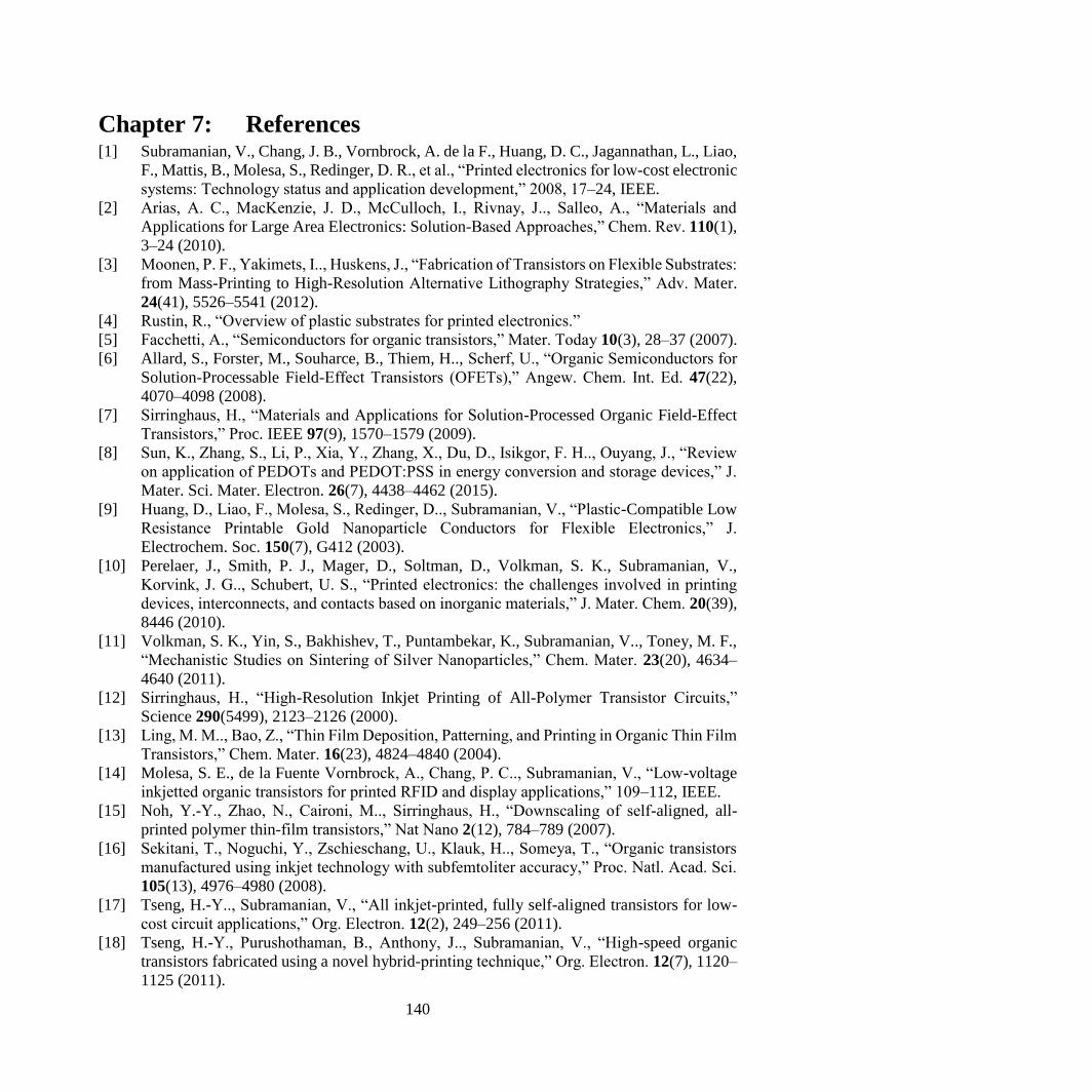
140
Chapter 7: References [1] Subramanian, V., Chang, J. B., Vornbrock, A. de la F., Huang, D. C., Jagannathan, L., Liao,
F., Mattis, B., Molesa, S., Redinger, D. R., et al., “Printed electronics for low-cost electronic
systems: Technology status and application development,” 2008, 17–24, IEEE.
[2] Arias, A. C., MacKenzie, J. D., McCulloch, I., Rivnay, J.., Salleo, A., “Materials and
Applications for Large Area Electronics: Solution-Based Approaches,” Chem. Rev. 110(1),
3–24 (2010).
[3] Moonen, P. F., Yakimets, I.., Huskens, J., “Fabrication of Transistors on Flexible Substrates:
from Mass-Printing to High-Resolution Alternative Lithography Strategies,” Adv. Mater.
24(41), 5526–5541 (2012).
[4] Rustin, R., “Overview of plastic substrates for printed electronics.”
[5] Facchetti, A., “Semiconductors for organic transistors,” Mater. Today 10(3), 28–37 (2007).
[6] Allard, S., Forster, M., Souharce, B., Thiem, H.., Scherf, U., “Organic Semiconductors for
Solution-Processable Field-Effect Transistors (OFETs),” Angew. Chem. Int. Ed. 47(22),
4070–4098 (2008).
[7] Sirringhaus, H., “Materials and Applications for Solution-Processed Organic Field-Effect
Transistors,” Proc. IEEE 97(9), 1570–1579 (2009).
[8] Sun, K., Zhang, S., Li, P., Xia, Y., Zhang, X., Du, D., Isikgor, F. H.., Ouyang, J., “Review
on application of PEDOTs and PEDOT:PSS in energy conversion and storage devices,” J.
Mater. Sci. Mater. Electron. 26(7), 4438–4462 (2015).
[9] Huang, D., Liao, F., Molesa, S., Redinger, D.., Subramanian, V., “Plastic-Compatible Low
Resistance Printable Gold Nanoparticle Conductors for Flexible Electronics,” J.
Electrochem. Soc. 150(7), G412 (2003).
[10] Perelaer, J., Smith, P. J., Mager, D., Soltman, D., Volkman, S. K., Subramanian, V.,
Korvink, J. G.., Schubert, U. S., “Printed electronics: the challenges involved in printing
devices, interconnects, and contacts based on inorganic materials,” J. Mater. Chem. 20(39),
8446 (2010).
[11] Volkman, S. K., Yin, S., Bakhishev, T., Puntambekar, K., Subramanian, V.., Toney, M. F.,
“Mechanistic Studies on Sintering of Silver Nanoparticles,” Chem. Mater. 23(20), 4634–
4640 (2011).
[12] Sirringhaus, H., “High-Resolution Inkjet Printing of All-Polymer Transistor Circuits,”
Science 290(5499), 2123–2126 (2000).
[13] Ling, M. M.., Bao, Z., “Thin Film Deposition, Patterning, and Printing in Organic Thin Film
Transistors,” Chem. Mater. 16(23), 4824–4840 (2004).
[14] Molesa, S. E., de la Fuente Vornbrock, A., Chang, P. C.., Subramanian, V., “Low-voltage
inkjetted organic transistors for printed RFID and display applications,” 109–112, IEEE.
[15] Noh, Y.-Y., Zhao, N., Caironi, M.., Sirringhaus, H., “Downscaling of self-aligned, all-
printed polymer thin-film transistors,” Nat Nano 2(12), 784–789 (2007).
[16] Sekitani, T., Noguchi, Y., Zschieschang, U., Klauk, H.., Someya, T., “Organic transistors
manufactured using inkjet technology with subfemtoliter accuracy,” Proc. Natl. Acad. Sci.
105(13), 4976–4980 (2008).
[17] Tseng, H.-Y.., Subramanian, V., “All inkjet-printed, fully self-aligned transistors for low-
cost circuit applications,” Org. Electron. 12(2), 249–256 (2011).
[18] Tseng, H.-Y., Purushothaman, B., Anthony, J.., Subramanian, V., “High-speed organic
transistors fabricated using a novel hybrid-printing technique,” Org. Electron. 12(7), 1120–
1125 (2011).

141
[19] Fukuda, K., Takeda, Y., Mizukami, M., Kumaki, D.., Tokito, S., “Fully Solution-Processed
Flexible Organic Thin Film Transistor Arrays with High Mobility and Exceptional
Uniformity,” Sci. Rep. 4, 3947 (2014).
[20] Fukuda, K., Takeda, Y., Yoshimura, Y., Shiwaku, R., Tran, L. T., Sekine, T., Mizukami,
M., Kumaki, D.., Tokito, S., “Fully-printed high-performance organic thin-film transistors
and circuitry on one-micron-thick polymer films,” Nat. Commun. 5 (2014).
[21] Yoshimura, Y., Takeda, Y., Fukuda, K., Kumaki, D.., Tokito, S., “High-speed operation in
printed organic inverter circuits with short channel length,” Org. Electron. 15(11), 2696–
2701 (2014).
[22] Grau, G., Kitsomboonloha, R., Swisher, S. L., Kang, H.., Subramanian, V., “Printed
Transistors on Paper: Towards Smart Consumer Product Packaging,” Adv. Funct. Mater.
24(32), 5067–5074 (2014).
[23] Kang, H., Kitsomboonloha, R., Ulmer, K., Stecker, L., Grau, G., Jang, J.., Subramanian, V.,
“Megahertz-class printed high mobility organic thin-film transistors and inverters on plastic
using attoliter-scale high-speed gravure-printed sub-5μm gate electrodes,” Org. Electron.
15(12), 3639–3647 (2014).
[24] Subramanian, V., Cen, J., de la Fuente Vornbrock, A., Grau, G., Kang, H., Kitsomboonloha,
R., Soltman, D.., Tseng, H.-Y., “High-Speed Printing of Transistors: From Inks to Devices,”
Proc. IEEE 103(4), 567–582 (2015).
[25] Fukuda, K., Yoshimura, Y., Okamoto, T., Takeda, Y., Kumaki, D., Katayama, Y.., Tokito,
S., “Reverse-Offset Printing Optimized for Scalable Organic Thin-Film Transistors with
Submicrometer Channel Lengths,” Adv. Electron. Mater. 1(8), 1500145 (2015).
[26] Grau, G., Kitsomboonloha, R., Kang, H.., Subramanian, V., “High performance printed
organic transistors using a novel scanned thermal annealing technology,” Org. Electron. 20,
150–157 (2015).
[27] Kitsomboonloha, R., Kang, H., Grau, G., Scheideler, W.., Subramanian, V., “MHz-Range
Fully Printed High-Performance Thin-Film Transistors by Using High-Resolution Gravure-
Printed Lines,” Adv. Electron. Mater. 1(12), 1500155 (2015).
[28] Grau, G.., Subramanian, V., “Fully High-Speed Gravure Printed, Low-Variability, High-
Performance Organic Polymer Transistors with Sub-5V Operation,” Adv. Electron. Mater.
2(4) (2016).
[29] Chang, J. B., Liu, V., Subramanian, V., Sivula, K., Luscombe, C., Murphy, A., Liu, J..,
Frechet, J. M. J., “Printable polythiophene gas sensor array for low-cost electronic noses,”
J. Appl. Phys. 100(1), 14506 (2006).
[30] Someya, T., Kato, Y., Sekitani, T., Iba, S., Noguchi, Y., Murase, Y., Kawaguchi, H..,
Sakurai, T., “Conformable, flexible, large-area networks of pressure and thermal sensors
with organic transistor active matrixes,” Proc. Natl. Acad. Sci. U. S. A. 102(35), 12321–
12325 (2005).
[31] Park, E. S., Chen, Y., Liu, T.-J. K.., Subramanian, V., “A New Switching Device for Printed
Electronics: Inkjet-Printed Microelectromechanical Relay,” Nano Lett. 13(11), 5355–5360
(2013).
[32] Chung, S., Ul Karim, M. A., Kwon, H.-J.., Subramanian, V., “High-Performance Inkjet-
Printed Four-Terminal Microelectromechanical Relays and Inverters,” Nano Lett. 15(5),
3261–3266 (2015).
142
[33] Braam, K.., Subramanian, V., “A Stencil Printed, High Energy Density Silver Oxide Battery
Using a Novel Photopolymerizable Poly(acrylic acid) Separator,” Adv. Mater. 27(4), 689–
694 (2015).
[34] Yang, J., Vak, D., Clark, N., Subbiah, J., Wong, W. W. H., Jones, D. J., Watkins, S. E..,
Wilson, G., “Organic photovoltaic modules fabricated by an industrial gravure printing
proofer,” Sol. Energy Mater. Sol. Cells 109, 47–55 (2013).
[35] Tekoglu, S., Hernandez-Sosa, G., Kluge, E., Lemmer, U.., Mechau, N., “Gravure printed
flexible small-molecule organic light emitting diodes,” Org. Electron. 14(12), 3493–3499
(2013).
[36] Cook, B. S.., Shamim, A., “Inkjet Printing of Novel Wideband and High Gain Antennas on
Low-Cost Paper Substrate,” IEEE Trans. Antennas Propag. 60(9), 4148–4156 (2012).
[37] McKerricher, G., Gonzalez Perez, J.., Shamim, A., “Fully Inkjet Printed RF Inductors and
Capacitors Using Polymer Dielectric and Silver Conductive Ink With Through Vias,” IEEE
Trans. Electron Devices 62(3), 1002–1009 (2015).
[38] Namsoo Lim., Jaeyoung Kim., Soojin Lee., Namyoung Kim., Gyoujin Cho., “Screen
Printed Resonant Tags for Electronic Article Surveillance Tags,” Adv. Packag. IEEE Trans.
On 32(1), 72–76 (2009).
[39] Sekitani, T., Nakajima, H., Maeda, H., Fukushima, T., Aida, T., Hata, K.., Someya, T.,
“Stretchable active-matrix organic light-emitting diode display using printable elastic
conductors,” Nat Mater 8(6), 494–499 (2009).
[40] Sekitani, T., Takamiya, M., Noguchi, Y., Nakano, S., Kato, Y., Sakurai, T.., Someya, T.,
“A large-area wireless power-transmission sheet using printed organic transistors and
plastic MEMS switches,” Nat Mater 6(6), 413–417 (2007).
[41] Krebs, F. C., “Fabrication and processing of polymer solar cells: A review of printing and
coating techniques,” Sol. Energy Mater. Sol. Cells 93(4), 394–412 (2009).
[42] Hambsch, M., Reuter, K., Stanel, M., Schmidt, G., Kempa, H., Fügmann, U., Hahn, U..,
Hübler, A. C., “Uniformity of fully gravure printed organic field-effect transistors,” Mater.
Sci. Eng. B 170(1–3), 93–98 (2010).
[43] Park, J.-U., Hardy, M., Kang, S. J., Barton, K., Adair, K., Mukhopadhyay, D. kishore., Lee,
C. Y., Strano, M. S., Alleyne, A. G., et al., “High-resolution electrohydrodynamic jet
printing,” Nat. Mater. 6(10), 782–789 (2007).
[44] Hannebauer, H., Dullweber, T., Falcon, T.., Brendel, R., “Fineline Printing Options for High
Efficiencies and Low Ag Paste Consumption,” Energy Procedia 38, 725–731 (2013).
[45] Erath, D., Filipović, A., Retzlaff, M., Goetz, A. K., Clement, F., Biro, D.., Preu, R.,
“Advanced screen printing technique for high definition front side metallization of
crystalline silicon solar cells,” Sol. Energy Mater. Sol. Cells 94(1), 57–61 (2010).
[46] “International Technology Roadmap for Photovoltaic (ITRPV), 2014 Results, Revision 1.”,
(2015).
[47] Joyce, M. J., Fleming III, P. D., Avuthu, S. G., Emamian, S., Eshkeiti, A., Atashbar, M..,
Donato, T., “Contribution of Flexo Process Variables to Fine Line Ag Electrode
Performance,” Int. J. Eng. Res. Technol. 3, ESRSA Publications (2014).
[48] Sung, D., de la Fuente Vornbrock, A.., Subramanian, V., “Scaling and Optimization of
Gravure-Printed Silver Nanoparticle Lines for Printed Electronics,” IEEE Trans. Compon.
Packag. Technol. 33(1), 105–114 (2010).
143
[49] Kitsomboonloha, R., Morris, S. J. S., Rong, X.., Subramanian, V., “Femtoliter-Scale
Patterning by High-Speed, Highly Scaled Inverse Gravure Printing,” Langmuir 28(48),
16711–16723 (2012).
[50] Nallan, H. C., Sadie, J. A., Kitsomboonloha, R., Volkman, S. K.., Subramanian, V.,
“Systematic Design of Jettable Nanoparticle-Based Inkjet Inks: Rheology, Acoustics, and
Jettability,” Langmuir 30(44), 13470–13477 (2014).
[51] Soltman, D., Smith, B., Kang, H., Morris, S. J. S.., Subramanian, V., “Methodology for
Inkjet Printing of Partially Wetting Films,” Langmuir 26(19), 15686–15693 (2010).
[52] Kang, H., Soltman, D.., Subramanian, V., “Hydrostatic optimization of inkjet-printed
films,” Langmuir 26(13), 11568–11573 (2010).
[53] Soltman, D., Smith, B., Morris, S. J. S.., Subramanian, V., “Inkjet printing of precisely
defined features using contact-angle hysteresis,” J. Colloid Interface Sci. 400, 135–139
(2013).
[54] de Gans, B.-J.., Schubert, U. S., “Inkjet Printing of Well-Defined Polymer Dots and Arrays,”
Langmuir 20(18), 7789–7793 (2004).
[55] Hu, H.., Larson, R. G., “Marangoni Effect Reverses Coffee-Ring Depositions,” J. Phys.
Chem. B 110(14), 7090–7094 (2006).
[56] Lim, J. A., Lee, W. H., Lee, H. S., Lee, J. H., Park, Y. D.., Cho, K., “Self-Organization of
Ink-jet-Printed Triisopropylsilylethynyl Pentacene via Evaporation-Induced Flows in a
Drying Droplet,” Adv. Funct. Mater. 18(2), 229–234 (2008).
[57] Soltman, D.., Subramanian, V., “Inkjet-Printed Line Morphologies and Temperature
Control of the Coffee Ring Effect,” Langmuir 24(5), 2224–2231 (2008).
[58] Janssen, D., De Palma, R., Verlaak, S., Heremans, P.., Dehaen, W., “Static solvent contact
angle measurements, surface free energy and wettability determination of various self-
assembled monolayers on silicon dioxide,” Thin Solid Films 515(4), 1433–1438 (2006).
[59] Cen, J., Kitsomboonloha, R.., Subramanian, V., “Cell Filling in Gravure Printing for Printed
Electronics,” Langmuir 30(45), 13716–13726 (2014).
[60] Bankoff, S. G., “Entrapment of gas in the spreading of a liquid over a rough surface,” AIChE
J. 4(1), 24–26 (1958).
[61] Reddy, S., Schunk, P. R.., Bonnecaze, R. T., “Dynamics of low capillary number interfaces
moving through sharp features,” Phys. Fluids 17(12), 122104 (2005).
[62] Brethour, J. M.., Benkeira, H., “Filling and Emptying of Gravure Cells – Experiment and
CFD Comparison,” presented at ISCST, 2002, Minneapolis.
[63] Noh, Y.-Y.., Sirringhaus, H., “Ultra-thin polymer gate dielectrics for top-gate polymer field-
effect transistors,” Org. Electron. 10(1), 174–180 (2009).
[64] Jung, Y., Kline, R. J., Fischer, D. A., Lin, E. K., Heeney, M., McCulloch, I.., DeLongchamp,
D. M., “The Effect of Interfacial Roughness on the Thin Film Morphology and Charge
Transport of High-Performance Polythiophenes,” Adv. Funct. Mater. 18(5), 742–750
(2008).
[65] Chabinyc, M. L., Lujan, R., Endicott, F., Toney, M. F., McCulloch, I.., Heeney, M., “Effects
of the surface roughness of plastic-compatible inorganic dielectrics on polymeric thin film
transistors,” Appl. Phys. Lett. 90(23), 233508 (2007).
[66] Kitsomboonloha, R.., Subramanian, V., “Lubrication-Related Residue as a Fundamental
Process Scaling Limit to Gravure Printed Electronics,” Langmuir 30(12), 3612–3624
(2014).

144
[67] Hariprasad, D., Grau, G., Schunk, R.., Tjiptowidjojo, K., “A computational model for
doctoring fluid films in gravure printing,” J. Appl. Phys. 119, 135303 (2016).
[68] Ceyhan, U.., Morris, S. J. S., “On tail formation during gravure printing of sessile drops,”
presented at 67th Annual Meeting of the APS Division of Fluid Dynamics, 2014, San
Francisco.
[69] Darhuber, A. A., Troian, S. M.., Wagner, S., “Physical mechanisms governing pattern
fidelity in microscale offset printing,” J. Appl. Phys. 90(7), 3602 (2001).
[70] Kapur, N., “A parametric study of direct gravure coating,” Chem. Eng. Sci. 58(13), 2875–
2882 (2003).
[71] Yin, X.., Kumar, S., “Flow visualization of the liquid emptying process in scaled-up gravure
grooves and cells,” Chem. Eng. Sci. 61(4), 1146–1156 (2006).
[72] Cai, S.., Bhushan, B., “Meniscus and viscous forces during normal separation of liquid-
mediated contacts,” Nanotechnology 18(46), 465704 (2007).
[73] Huang, W.-X., Lee, S.-H., Sung, H. J., Lee, T.-M.., Kim, D.-S., “Simulation of liquid
transfer between separating walls for modeling micro-gravure-offset printing,” Int. J. Heat
Fluid Flow 29(5), 1436–1446 (2008).
[74] Hoda, N.., Kumar, S., “Boundary integral simulations of liquid emptying from a model
gravure cell,” Phys. Fluids 20(9), 92106 (2008).
[75] Kang, H. W., Sung, H. J., Lee, T.-M., Kim, D.-S.., Kim, C.-J., “Liquid transfer between two
separating plates for micro-gravure-offset printing,” J. Micromechanics Microengineering
19(1), 15025 (2009).
[76] Dodds, S., Carvalho, M. da S.., Kumar, S., “Stretching and slipping of liquid bridges near
plates and cavities,” Phys. Fluids 21(9), 92103 (2009).
[77] Ghadiri, F., Ahmed, D. H., Sung, H. J.., Shirani, E., “Non-Newtonian ink transfer in
gravure–offset printing,” Int. J. Heat Fluid Flow 32(1), 308–317 (2011).
[78] Ahmed, D. H., Sung, H. J.., Kim, D.-S., “Simulation of non-Newtonian ink transfer between
two separating plates for gravure-offset printing,” Int. J. Heat Fluid Flow 32(1), 298–307
(2011).
[79] Sankaran, A. K.., Rothstein, J. P., “Effect of viscoelasticity on liquid transfer during gravure
printing,” J. Non-Newton. Fluid Mech. 175–176, 64–75 (2012).
[80] Nguyen, H. A. D., Lee, C., Shin, K.-H.., Lee, D., “An Investigation of the Ink-Transfer
Mechanism During the Printing Phase of High-Resolution Roll-to-Roll Gravure Printing,”
IEEE Trans. Compon. Packag. Manuf. Technol. 5(10), 1516–1524 (2015).
[81] Kumar, S., “Liquid Transfer in Printing Processes: Liquid Bridges with Moving Contact
Lines,” Annu. Rev. Fluid Mech. 47(1), 67–94 (2015).
[82] Grau, G., Cen, J., Kang, H., Kitsomboonloha, R., Scheideler, W. J.., Subramanian, V.,
“Gravure-printed electronics: Recent progress in tooling development, understanding of
printing physics, and realization of printed devices,” Flex. Print. Electron. (invited review
under review).
[83] Kang, H., Kitsomboonloha, R., Jang, J.., Subramanian, V., “High-Performance Printed
Transistors Realized Using Femtoliter Gravure-Printed Sub-10 μm Metallic Nanoparticle
Patterns and Highly Uniform Polymer Dielectric and Semiconductor Layers,” Adv. Mater.
24(22), 3065–3069 (2012).
[84] Minemawari, H., Yamada, T., Matsui, H., Tsutsumi, J. ’ya., Haas, S., Chiba, R., Kumai, R..,
Hasegawa, T., “Inkjet printing of single-crystal films,” Nature 475(7356), 364–367 (2011).

145
[85] Yuan, Y., Giri, G., Ayzner, A. L., Zoombelt, A. P., Mannsfeld, S. C. B., Chen, J., Nordlund,
D., Toney, M. F., Huang, J., et al., “Ultra-high mobility transparent organic thin film
transistors grown by an off-centre spin-coating method,” Nat. Commun. 5, 3005 (2014).
[86] de la Fuente Vornbrock, A., Sung, D., Kang, H., Kitsomboonloha, R.., Subramanian, V.,
“Fully gravure and ink-jet printed high speed pBTTT organic thin film transistors,” Org.
Electron. 11(12), 2037–2044 (2010).
[87] Sirringhaus, H., Kawase, T., Friend, R. H., Shimoda, T., Inbasekaran, M., Wu, W.., Woo,
E. P., “High-Resolution Inkjet Printing of All-Polymer Transistor Circuits,” Science
290(5499), 2123–2126 (2000).
[88] Noh, Y.-Y., Zhao, N., Caironi, M.., Sirringhaus, H., “Downscaling of self-aligned, all-
printed polymer thin-film transistors,” Nat. Nanotechnol. 2(12), 784–789 (2007).
[89] Sele, C. W., von Werne, T., Friend, R. H.., Sirringhaus, H., “Lithography-Free, Self-Aligned
Inkjet Printing with Sub-Hundred-Nanometer Resolution,” Adv. Mater. 17(8), 997–1001
(2005).
[90] Tobjörk, D.., Österbacka, R., “Paper Electronics,” Adv. Mater. 23, 1935–1961 (2011).
[91] Kim, J.-Y., Park, S. H., Jeong, T., Bae, M. J., Song, S., Lee, J., Han, I. T., Jung, D.., Yu, S.,
“Paper as a Substrate for Inorganic Powder Electroluminescence Devices,” IEEE Trans.
Electron Devices 57(6), 1470–1474 (2010).
[92] Lim, W., Douglas, E. A., Norton, D. P., Pearton, S. J., Ren, F., Heo, Y.-W., Son, S. Y..,
Yuh, J. H., “Low-voltage indium gallium zinc oxide thin film transistors on paper
substrates,” Appl. Phys. Lett. 96(5), 53510 (2010).
[93] Lamprecht, B., Thünauer, R., Ostermann, M., Jakopic, G.., Leising, G., “Organic
photodiodes on newspaper,” Phys. Status Solidi A 202(5), R50–R52 (2005).
[94] Yong-Hoon Kim., Dae-Gyu Moon., Jeong-In Han., “Organic TFT array on a paper
substrate,” Electron Device Lett. IEEE 25(10), 702–704 (2004).
[95] Kim, Y. H., Moon, D. G., Kim, W. K.., Han, J. I., “Organic thin-film devices on paper
substrates,” J. Soc. Inf. Disp. 13(10), 829–833 (2005).
[96] Li, Y., Liu, C., Xu, Y., Minari, T., Darmawan, P.., Tsukagoshi, K., “Solution-processed
organic crystals for field-effect transistor arrays with smooth semiconductor/dielectric
interface on paper substrates,” Org. Electron. 13(5), 815–819 (2012).
[97] Zhang, T., Wang, X., Li, T., Guo, Q.., Yang, J., “Fabrication of flexible copper-based
electronics with high-resolution and high-conductivity on paper via inkjet printing,” J.
Mater. Chem. C 2(2), 286 (2014).
[98] Lim, W., Douglas, E. A., Kim, S.-H., Norton, D. P., Pearton, S. J., Ren, F., Shen, H.., Chang,
W. H., “High mobility InGaZnO[sub 4] thin-film transistors on paper,” Appl. Phys. Lett.
94(7), 72103 (2009).
[99] Zschieschang, U., Yamamoto, T., Takimiya, K., Kuwabara, H., Ikeda, M., Sekitani, T.,
Someya, T.., Klauk, H., “Organic Electronics on Banknotes,” Adv. Mater. 23(5), 654–658
(2011).
[100] Harting, M., Zhang, J., Gamota, D. R.., Britton, D. T., “Fully printed silicon field effect
transistors,” Appl. Phys. Lett. 94(19), 193509 (2009).
[101] Yoon, B., Ham, D.-Y., Yarimaga, O., An, H., Lee, C. W.., Kim, J.-M., “Inkjet Printing of
Conjugated Polymer Precursors on Paper Substrates for Colorimetric Sensing and Flexible
Electrothermochromic Display,” Adv. Mater. 23(46), 5492–5497 (2011).
[102] Lee, C.-G.., Dodabalapur, A., “Solution-Processed High-k Dielectric, ZrO2, and Integration
in Thin-Film Transistors,” J. Electron. Mater. 41(5), 895–898 (2012).
146
[103] Li, X., Ballerini, D. R.., Shen, W., “A perspective on paper-based microfluidics: Current
status and future trends,” Biomicrofluidics 6(1), 11301-011301–011313 (2012).
[104] Molesa, S. E., De La Fuente Vornbrock, A., Chang, P. C.., Subramanian, V., “Low-voltage
inkjetted organic transistors for printed RFID and display applications,” Tech. Dig. - Int.
Electron Devices Meet. IEDM 2005, 109–112, IEEE (2005).
[105] Klauk, H., Halik, M., Zschieschang, U., Schmid, G., Radlik, W.., Weber, W., “High-
mobility polymer gate dielectric pentacene thin film transistors,” J. Appl. Phys. 92(9), 5259
(2002).
[106] Grau, G.., Subramanian, V., “Effect of substrate roughness on the performance of printed
OTFTs on paper substrates,” presented at MRS Fall Meeting, 3 December 2013, Boston.
[107] McCulloch, I., Heeney, M., Bailey, C., Genevicius, K., MacDonald, I., Shkunov, M.,
Sparrowe, D., Tierney, S., Wagner, R., et al., “Liquid-crystalline semiconducting polymers
with high charge-carrier mobility,” Nat. Mater. 5(4), 328–333 (2006).
[108] Xue, F., Liu, Z., Su, Y.., Varahramyan, K., “Inkjet printed silver source/drain electrodes for
low-cost polymer thin film transistors,” Microelectron. Eng. 83(2), 298–302 (2006).
[109] Kline, R. J., DeLongchamp, D. M., Fischer, D. A., Lin, E. K., Heeney, M., McCulloch, I..,
Toney, M. F., “Significant dependence of morphology and charge carrier mobility on
substrate surface chemistry in high performance polythiophene semiconductor films,” Appl.
Phys. Lett. 90(6), 62117 (2007).
[110] Hennig, G., Selbmann, K.-H.., Brockelt, A., “Laser engraving in gravure industry,” Proc
SPIE 6157, W. Gries and T. P. Pearsall, Eds., 61570C–61570C–14 (2005).
[111] Clark, D. A., “Major Trends in Gravure Printed Electronics,” California Polytechnic State
University (2010).
[112] Gravure Association of America., Gravure Education Foundation, eds., Gravure: process
and technology, Gravure Association of America, Rochester, NY (1991).
[113] Grau, G., Scheideler, W. J.., Subramanian, V., “High-resolution gravure printed lines:
Proximity effects and design rules,” Proc SPIE 9569, 95690B–1, San Diego (2015).
[114] Zhang, H., Ramm, A., Lim, S., Xie, W., Ahn, B. Y., Xu, W., Mahajan, A., Suszynski, W.
J., Kim, C., et al., “Wettability Contrast Gravure Printing,” Adv. Mater. 27(45), 7420–7425
(2015).
[115] Grau, G., Kitsomboonloha, R.., Subramanian, V., “Fabrication of a high-resolution roll for
gravure printing of 2µm features,” Proc SPIE 9568, 95680M, San Diego (2015).
[116] Arya, S. P. S.., D’Amico, A., “Preparation, properties and applications of boron nitride thin
films,” Thin Solid Films 157(2), 267–282 (1988).
[117] Ploof, L., “Electroless Nickel Composite Coatings,” Adv. Mater. Process. 166(5), 36–38
(2008).
[118] Buchheit, T. E., Goods, S. H., Kotula, P. G.., Hlava, P. F., “Electrodeposited 80Ni–20Fe
(Permalloy) as a structural material for high aspect ratio microfabrication,” Mater. Sci. Eng.
A 432(1–2), 149–157 (2006).
[119] Choi, S.-J., Kim, H. N., Bae, W. G.., Suh, K.-Y., “Modulus- and surface energy-tunable
ultraviolet-curable polyurethane acrylate: properties and applications,” J. Mater. Chem.
21(38), 14325 (2011).
[120] Pforr, R., Ronse, K. G., Van den Hove, L., Yen, A., Palmer, S. R., Fuller, G. E.., Otto, O.
W., “Feature biasing versus feature-assisted lithography: a comparison of proximity
correction methods for 0.5*(lambda/NA) lithography,” Proc SPIE 2440 Opt. Microlithogr.
VIII, T. A. Brunner, Ed., 150–170 (1995).
147
[121] Garofalo, J., “Mask assisted off-axis illumination technique for random logic,” J. Vac. Sci.
Technol. B Microelectron. Nanometer Struct. 11(6), 2651 (1993).
[122] Fung Chen, J., “Optical proximity correction for intermediate-pitch features using sub-
resolution scattering bars,” J. Vac. Sci. Technol. B Microelectron. Nanometer Struct. 15(6),
2426 (1997).
[123] Chen, J. F., Laidig, T. L., Wampler, K. E.., Caldwell, R. F., “Practical method for full-chip
optical proximity correction,” Proc SPIE 3051 Opt. Microlithogr. X, G. E. Fuller, Ed., 790–
803 (1997).
[124] Bornemann, N., “Characterization and Investigation of Large-Area, Ultra-Thin Gravure
Printed Layers,” PhD thesis, Technische Universitat Darmstadt (2014).
[125] Saffman, P. G.., Taylor, G., “The Penetration of a Fluid into a Porous Medium or Hele-
Shaw Cell Containing a More Viscous Liquid,” Proc. R. Soc. Math. Phys. Eng. Sci.
245(1242), 312–329 (1958).
[126] Tabeling, P., Zocchi, G.., Libchaber, A., “An experimental study of the Saffman-Taylor
instability,” J. Fluid Mech. 177(1), 67 (1987).
[127] Voß, C., “Analytische Modellierung, experimentelle Untersuchungen und dreidimensionale
Gitter-Boltzmann Simulation der quasistatischen und instabilen Farbspaltung,” PhD thesis,
Bergischen Universität Gesamthochschule Wuppertal (2002).
[128] Reuter, K., Kempa, H., Brandt, N., Bartzsch, M.., Huebler, A. C., “Influence of process
parameters on the electrical properties of offset printed conductive polymer layers,” Prog.
Org. Coat. 58(4), 312–315 (2007).
[129] Bornemann, N., Sauer, H. M.., Dörsam, E., “Gravure Printed Ultrathin Layers of Small-
Molecule Semiconductors on Glass,” J. Imaging Sci. Technol. 55(4), 40201 (2011).
[130] Hernandez-Sosa, G., Bornemann, N., Ringle, I., Agari, M., Dörsam, E., Mechau, N..,
Lemmer, U., “Rheological and Drying Considerations for Uniformly Gravure-Printed
Layers: Towards Large-Area Flexible Organic Light-Emitting Diodes,” Adv. Funct. Mater.
23(25), 3164–3171 (2013).
[131] Anthony, J. E., Eaton, D. L.., Parkin, S. R., “A Road Map to Stable, Soluble, Easily
Crystallized Pentacene Derivatives,” Org. Lett. 4(1), 15–18 (2002).
[132] Hamilton, R., Smith, J., Ogier, S., Heeney, M., Anthony, J. E., McCulloch, I., Veres, J.,
Bradley, D. D. C.., Anthopoulos, T. D., “High-Performance Polymer-Small Molecule Blend
Organic Transistors,” Adv. Mater. 21(10–11), 1166–1171 (2009).
[133] Smith, J., Hamilton, R., McCulloch, I., Stingelin-Stutzmann, N., Heeney, M., Bradley, D.
D. C.., Anthopoulos, T. D., “Solution-processed organic transistors based on
semiconducting blends,” J. Mater. Chem. 20(13), 2562 (2010).
[134] Hatano, M., Moon, S., Lee, M., Suzuki, K.., Grigoropoulos, C. P., “Excimer laser-induced
temperature field in melting and resolidification of silicon thin films,” J. Appl. Phys. 87(1),
36 (2000).
[135] Lee, M., Moon, S.., Grigoropoulos, C. P., “In situ visualization of interface dynamics during
the double laser recrystallization of amorphous silicon thin films,” J. Cryst. Growth 226(1),
8–12 (2001).
[136] Ryu, S.-G., Gruber, I., Grigoropoulos, C. P., Poulikakos, D.., Moon, S.-J., “Large area
crystallization of amorphous Si with overlapping high repetition rate laser pulses,” Thin
Solid Films 520(22), 6724–6729 (2012).
148
[137] Lee, M., Moon, S., Hatano, M., Suzuki, K.., Grigoropoulos, C. P., “Relationship between
fluence gradient and lateral grain growth in spatially controlled excimer laser crystallization
of amorphous silicon films,” J. Appl. Phys. 88(9), 4994 (2000).
[138] Sposili, R. S.., Im, J. S., “Sequential lateral solidification of thin silicon films on SiO2,”
Appl. Phys. Lett. 69(19), 2864 (1996).
[139] Liu, C.-Y.., Bard, A. J., “In-Situ Regrowth and Purification by Zone Melting of Organic
Single-Crystal Thin Films Yielding Significantly Enhanced Optoelectronic Properties,”
Chem. Mater. 12(8), 2353–2362 (2000).
[140] Schweicher, G., Paquay, N., Amato, C., Resel, R., Koini, M., Talvy, S., Lemaur, V., Cornil,
J., Geerts, Y., et al., “Toward Single Crystal Thin Films of Terthiophene by Directional
Crystallization Using a Thermal Gradient,” Cryst. Growth Des. 11(8), 3663–3672 (2011).
[141] Natsume, Y., Minakata, T.., Aoyagi, T., “Pentacene thin film transistors fabricated by
solution process with directional crystal growth,” Org. Electron. 10(1), 107–114 (2009).
[142] Becerril, H. A., Roberts, M. E., Liu, Z., Locklin, J.., Bao, Z., “High‐Performance Organic
Thin‐Film Transistors through Solution‐Sheared Deposition of Small‐Molecule Organic
Semiconductors,” Adv. Mater. 20(13), 2588–2594 (2008).
[143] Soeda, J., Uemura, T., Okamoto, T., Mitsui, C., Yamagishi, M.., Takeya, J., “Inch-Size
Solution-Processed Single-Crystalline Films of High-Mobility Organic Semiconductors,”
Appl. Phys. Express 6(7), 76503 (2013).
[144] Tracz, A., Jeszka, J. K., Watson, M. D., Pisula, W., Müllen, K.., Pakula, T., “Uniaxial
Alignment of the Columnar Super-Structure of a Hexa (Alkyl) Hexa-peri-
hexabenzocoronene on Untreated Glass by Simple Solution Processing,” J. Am. Chem. Soc.
125(7), 1682–1683 (2003).
[145] Pisula, W., Menon, A., Stepputat, M., Lieberwirth, I., Kolb, U., Tracz, A., Sirringhaus, H.,
Pakula, T.., Müllen, K., “A Zone-Casting Technique for Device Fabrication of Field-Effect
Transistors Based on Discotic Hexa-peri-hexabenzocoronene,” Adv. Mater. 17(6), 684–689
(2005).
[146] Miskiewicz, P., Mas-Torrent, M., Jung, J., Kotarba, S., Glowacki, I., Gomar-Nadal, E.,
Amabilino, D. B., Veciana, J., Krause, B., et al., “Efficient High Area OFETs by Solution
Based Processing of a π-Electron Rich Donor,” Chem. Mater. 18(20), 4724–4729 (2006).
[147] Duffy, C. M., Andreasen, J. W., Breiby, D. W., Nielsen, M. M., Ando, M., Minakata, T..,
Sirringhaus, H., “High-Mobility Aligned Pentacene Films Grown by Zone-Casting,” Chem.
Mater. 20(23), 7252–7259 (2008).
[148] Miskiewicz, P., Kotarba, S., Jung, J., Marszalek, T., Mas-Torrent, M., Gomar-Nadal, E.,
Amabilino, D. B., Rovira, C., Veciana, J., et al., “Influence of SiO2 surface energy on the
performance of organic field effect transistors based on highly oriented, zone-cast layers of
a tetrathiafulvalene derivative,” J. Appl. Phys. 104(5), 54509 (2008).
[149] Tszydel, I., Kucinska, M., Marszalek, T., Rybakiewicz, R., Nosal, A., Jung, J., Gazicki-
Lipman, M., Pitsalidis, C., Gravalidis, C., et al., “High-Mobility and Low Turn-On Voltage
n-Channel OTFTs Based on a Solution-Processable Derivative of Naphthalene Bisimide,”
Adv. Funct. Mater. 22(18), 3840–3844 (2012).
[150] Keum, C.-M., Kwon, J.-H., Lee, S.-D.., Bae, J.-H., “Control of the molecular order and
cracks of the 6,13-bis(triisopropylsilylethynyl)-pentacene on a polymeric insulator by
anisotropic solvent drying,” Solid-State Electron. 89, 189–193 (2013).
149
[151] Yoon, M.-H., Yan, H., Facchetti, A.., Marks, T. J., “Low-Voltage Organic Field-Effect
Transistors and Inverters Enabled by Ultrathin Cross-Linked Polymers as Gate Dielectrics,”
J. Am. Chem. Soc. 127(29), 10388–10395 (2005).
[152] Park, Y. D., Kim, D. H., Jang, Y., Hwang, M., Lim, J. A.., Cho, K., “Low-voltage polymer
thin-film transistors with a self-assembled monolayer as the gate dielectric,” Appl. Phys.
Lett. 87(24), 243509 (2005).
[153] Lai, S., Cosseddu, P., Gazzadi, G. C., Barbaro, M.., Bonfiglio, A., “Towards high frequency
performances of ultra-low voltage OTFTs: Combining self-alignment and hybrid, nanosized
dielectrics,” Org. Electron. 14(3), 754–761 (2013).
[154] Pierre, A., Sadeghi, M., Payne, M. M., Facchetti, A., Anthony, J. E.., Arias, A. C., “All-
Printed Flexible Organic Transistors Enabled by Surface Tension-Guided Blade Coating,”
Adv. Mater. 26(32), 5722–5727 (2014).
[155] Park, S. K., Jackson, T. N., Anthony, J. E.., Mourey, D. A., “High mobility solution
processed 6,13-bis(triisopropyl-silylethynyl) pentacene organic thin film transistors,” Appl.
Phys. Lett. 91(6), 63514 (2007).
[156] Hansen, C. M., “50 Years with solubility parameters—past and future,” Prog. Org. Coat.
51(1), 77–84 (2004).
[157] Hansen, C. M., “Aspects of solubility, surfaces and diffusion in polymers,” Prog. Org. Coat.
51(1), 55–66 (2004).
[158] Gaikwad, A. M., Khan, Y., Ostfeld, A. E., Pandya, S., Abraham, S.., Arias, A. C.,
“Identifying orthogonal solvents for solution processed organic transistors,” Org. Electron.
30, 18–29 (2016).
[159] Hansen, C. M., Hansen solubility parameters: a user’s handbook, 2nd ed, CRC Press, Boca
Raton (2007).
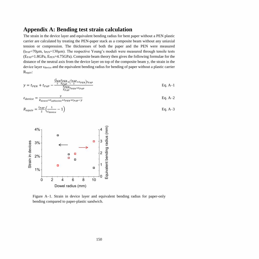
150
Appendix A: Bending test strain calculation The strain in the device layer and equivalent bending radius for bent paper without a PEN plastic
carrier are calculated by treating the PEN-paper stack as a composite beam without any uniaxial
tension or compression. The thicknesses of both the paper and the PEN were measured
(tPAP=70µm, tPEN=130µm). The respective Young’s moduli were measured through tensile tests
(EPAP=1.8GPa, EPEN=4.75GPa). Composite beam theory then gives the following formulae for the
distance of the neutral axis from the device layer on top of the composite beam y, the strain in the
device layer εdevice and the equivalent bending radius for bending of paper without a plastic carrier
Requiv:
𝑦 = 𝑡𝑃𝐸𝑁 + 𝑡𝑃𝐴𝑃 −
𝑡𝑃𝐸𝑁2
2
𝐸𝑃𝐸𝑁𝐸𝑃𝐴𝑃
+(𝑡𝑃𝐴𝑃
2+𝑡𝑃𝐸𝑁)𝑡𝑃𝐴𝑃
𝐸𝑃𝐸𝑁𝐸𝑃𝐴𝑃
𝑡𝑃𝐸𝑁+𝑡𝑃𝐴𝑃
Eq. A–1
휀𝑑𝑒𝑣𝑖𝑐𝑒 =𝑦
𝑅𝑑𝑜𝑤𝑒𝑙+𝑡𝑎𝑑ℎ𝑒𝑠𝑖𝑣𝑒+𝑡𝑃𝐸𝑁+𝑡𝑃𝐴𝑃−𝑦 Eq. A–2
𝑅𝑒𝑞𝑢𝑖𝑣 =𝑡𝑃𝐴𝑃
2(
1
𝜀𝑑𝑒𝑣𝑖𝑐𝑒− 1) Eq. A–3
0 2 4 6 8 10
1%
2%
3%
4%
Str
ain
in
devic
es
Dowel radius (mm)
0
1
2
3
4
Equ
iva
lent be
nd
ing r
ad
ius (
mm
)
Figure A–1. Strain in device layer and equivalent bending radius for paper-only
bending compared to paper-plastic sandwich.