gs gd ) c:r c.i1)aries.ucsd.edu/najmabadi/class/ece102/11-w/lab/ece... · structions to assist in...
TRANSCRIPT
unity. For the MOSFET, IT = gml2 ~Cgs + Cgd ) , and for the BJT,fT = gml2 7t( C:r + C.I1) .
• The internal capacitances of the MOSFET and the BJT cause the amplifier gain to fall off at high frequencies. An estimate of the amplifier bandwidth is provided by the frequency IH at which the gain drops 3 dB below its value at midband, AM. A figure-of-merit for the amplifier is the gain-bandwidth product G B = AM fH. Usually, it is possible to trade offgain for increased bandwidth, with GB remaining nearly constant. For amplifiers with a dominant pole with frequency IH' the gain falls off at a uniform 6-dB/octave (20-dB/decade) rate, reaching 0 dB at t; = GB.
• The high-frequency response of the CS and CE amplifiers is severely limited by the Miller effect: The small capacitance Cgd (C.I1) is multiplied by a factor approximately equal to the gain from gate to drain (base to collector) gmR~ and thus gives rise to a large capacitance at the amplifier input. The increased Cin interacts with the effective signal-source resistance R~ig and causes the amplifier gain to have a 3-dB frequency IH = 1I27tR~igCin .
• The method of open-circuit time constants provides a simple and powerful way to obtain a reasonably good estimate of the upper 3-dB frequency IH . The capacitors that limit the high-frequency response are considered one at time with Vsig = 0 and all the other capacitances set to zero (open circuited). The resistance seen by each capacitance is determined, and the overall time constant rH is obtained by summing the individual
time constants. Then/H is found as 112 JrrH .
9.10 Multistage Amplifier Examples 785
• The CG and CB amplifiers do not suffer from the Miller effect. Thus the cascode amplifier, which consists of a cascade of a CS and CG stages (CE and CB stages), can be designed to obtain wider bandwidth than that achieved in the CS (CE) amplifier alone. The key, however, is to design the cascode so that the gain obtained in the CS (CE) stage is minimized.
• The source and emitter followers do not suffer from the Miller effect and thus feature wide bandwidths.
• The high-frequency response of the differential amplifier can be obtained by considering the differential and common-mode half-circuits. The CMRR falls offat a relatively low frequency determined by the output impedance of the bias current source.
• The high-frequency response ofthe current-mirror-loaded differential amplifier is complicated by the fact that there are two signal paths between input and output: a direct path and one through the current mirror.
• Combining two transistors in a way that eliminates or minimizes the Miller effect can result in a much wider bandwidth. Some such configurations are presented in Section 9.9.
• The key to the analysis of the high-frequency response of a multistage amplifier is to use simple macro models to estimate the frequencies of the poles formed at the interface between each two stages, in addition to the input and output poles. The pole with the lowest frequency dominates and determines IH . I
I l
~
"'---------~-Computer Simulation Problems
IImI Problems identified by this icon are intended to demonstrate the value of using SPICE simulation to verify hand analysis and design, and to investigate important issues such as gain- bandwidth tradeoff. Instructions to assist in setting up PSpice and Multisim simulations for all the indicated problems can be found in the corresponding files on the disc. Note that ifa particular parameter value is not specified in the problem statement, you are to make a reasonable assumption. *difficult problem; ** more difficult; *** very challenging and/or time-consuming; D: design problem.
, Section 9.1: Low-Frequency Response of the CS and CE Amplifiers
o 9.1 The amplifier in Fig. P9.1 is biased to operate at gm = 1 mAN. Neglecting ro' find the midband gain. Find the value of Cs that places h at 20 Hz.
9.2 Consider the amplifier of Fig. 9.2(a). Let RD = 10 ill, ro = 100 ill, and RL = 10 ill. Find the value of CC2' specified to one significant digit, to ensure that the associated break frequency is at, or below, 10 Hz. Ifa higher-power design results in doubling 1D, with both RD and ro reduced by a factor of 2, what does the comer frequency (due to CC2) become? For

786 Chapter 9 Frequency Response
V\
~ W ..J m o a: A.
G\
III: w tea. V'TC :z: u
Figure P9.1
Voo
Ro
Cs
RS~ 6 kil
= 10 kil
Vo
-Vss
increasingly higher-power designs, what is the highest corner frequency that can be associated with Co?
9.3 The NMOS transistor in the discrete CS amplifier circuit
ofFig. P9.3 is biased to have gm = 5 mAN. FindAM>hIJP2JPJ' andk
VDD
47 Mil 4.7kil
100kil O.Ip,F:FVOlOkil
I
Vsig Ito-' Figure P9.3
o 9.4 Consider the low-frequency response of the CS amplifier of Fig. 9.2(a). Let Rsig = 0.5 MO, Ra =2 MO, gm = 3 mAN, RD = 20 ill, and RL = 10 ill. Find AM" Also, design the coupling and bypass capacitors to locate the three lowfrequency poles at 50 Hz, 10 Hz, and 3 Hz. Use a minimum total capacitance, with capacitors specified only to a single significant digit. What value ofh results?
o 9.5 A particular version of the CS amplifier in Fig. 9.2 uses a transistor biased to operate with gm = 5 mAN. Resistances Rsig = 200kQ, RG = 10MQ, RD = 3 kQ, and RL = 5 kQ . As an initial design, the circuit designer selects
CCI = CC2 = Cs = IIJ.F. Find the frequencieslpl' IP2, and Ip3 and rank them in order of frequency, highest first. Cal
culate the ratios ofthe first to second, and second to third. The final design requires that the first pole dominate at 10Hz with the second a factor of 4 lower, and the third another a factor of 4 lower. Find the values of all the capacitances and the total capacitance needed. If the separation factor were 10, what capacitor values and total capacitance would be needed? (Note: You can see that the total capacitance need not be much larger to spread the poles, as is desired in certain applications.)
o 9.6 Repeat Example 9.1 to find Cs , CC! , and CC2 that provide IL = 20 Hz and the other pole frequencies at 4 Hz and 1 Hz. Design to keep the total capacitance to a minimum.
o 9.7 Reconsider Exercise 9.1 with the aim offmding a better-performing design using the same total capacitance, that is, 3 IlF. Prepare a design in which the break frequencies are separated by a factor of 5 (i.e.,/, Jl5, andJl25). What are the three capacitor values, the three break frequencies, and IL that you achieve?
9.8 Repeat Exercise 9.2 for the situation in which CE = 50
IlF and CCI = CC2 = 2 IlF. Find the three break frequencies and estimate IL . o 9.9 Repeat Example 9.2 for a related CE amplifier whose supply voltages and bias current are each reduced to half their original value butRB , Rc ,Rsig , andRL are left unchanged. FindCC! ,CE , and CC2 for IL = 100 Hz. Minimize the total capacitance used, under the following conditions. Arrange that
the contributions of CE , C CI , and C C2 are 80%, 10%, and 10%, respectively. SpecifY capacitors to two significant digits, choosing the next highest value, in general, for a conservative design, but realizing that for C E, this may represent a larger capacitance increment. Check the value of IL that results. [Note: An attractive approach can be to select C E on the small side, allowing it to contribute more than 80% to IL, while making CCI and CC21arger, since they must contribute less to
IL .) o 9.10 A particular current-biased CE amplifier operating at 100llA from ±3 -V power supplies employs Rc = 20 kO, RB = 200 kQ ; it operates between a 20-kQ source and a 10k Q load. The transistor fJ = 100. Select C E first for a minimum value specified to one significant digit and providing
up to 90% of IL .Then choose C C I and C C2 , each specified to one significant digit, with the goal of minimizing the total capacitance used. What IL results? What total capacitance is needed?
9.11 Consider the common-emitter amplifier of Fig. P9.11 under the following conditions: Rsig = 5 ill, RI = 33 ill, R2 =22 ill, R£ =3.9 ill, Re =4.7 ill, RL =5.6 ill, Vee =5 V. The dc emitter current can be shown to be 1£ = 0.3 rnA, at which fJ = 120. Find the input resistance Rin and the midband gain AM" If CC! =Co =1 IlF and CE =20 !1F, find the three break frequencieshIJP2' andfPJ and an estimate fork Note that RE has to be taken into account in evaluatingh2.
~
Section 9.3: High-Frequency Response of the CS and CE Amplifiers
9.29 In a particular common-source amplifier for which the midband voltage gain between gate and drain (i.e., -gmR~ ) is -29 VN, the NMOS transistor has Cgs = 0.5 pF and Cgd = 0.1 pF. What input capacitance would you expect? For what range of signal-source resistances can you expect the 3-dB frequency to exceed 10 MHz? Neglect the effect of RG .
o 9.30 A design is required for a CS amplifier for which the MOSFET is operated at gm = 5 mAN and hasCgs = 5 pF and Cgd = 1 pF. The amplifier is fed with a signal source having Rsig = I kQ, andRG is very large. What is the largest value of R~ for which the upper 3-dB frequency is at least 10 MHz? What is the corresponding value of midband gain and gain-bandwidth product? Ifthe specification on the upper 3-dB frequency can be relaxed by a factor of 3, that is, to (10/3) MHz, what can AM and GB become?
9.31 Reconsider Example 9.3 for the situation in which the transistor is replaced by one whose width W is half that of the original transistor while the bias current remains unchanged. Find modified values for all the device parameters along withA M, fH' and the gain-bandwidth product, GB. Contrast this with the original design by calculating the ratios of new value to old for W, Vov , gm' Cgs , Cgd , Cin ,
AM,[H' and GB.
o 9.32 In a CS amplifier, such as that in Fig. 9.2(a), the resistance of the source R,;g = 100 ill, anlplifier input resistance (which is due to the biasing network) R;n = 100 ill, Cg, = 1 pF, Cgd = 0.2 pF, gm = 3 mAN, ro = 50 ill, RD = 8 ill, and RL = 10 ill. Determine the expected 3-dB cutoff frequency fH and the midband gain. In evaluating ways to doublefH' a designer considers the alternatives of changing either RL or Rm. To raise IH as described, what separate change in each would be required? What midband voltage gain results in each case?
9.33 A discrete MOSFET common-source amplifier has RG = I Mn, gm = 5 mAN, ro = 100 ill, RD = 10 ill, Cg, = 2 pF, and Cgd= 0.4 pF. The amplifier is fed from a voltage source with an internal resistance of 500 ill and is connected to a 10-ill load. Find:
(a) the overall midband gain AM (b) the upper 3-dB frequency IH
9.34 The analysis ofthe high-frequency response ofthe common-source amplifier, presented in the text, is based on the assumption that the resistance ofthe signal source, R~g' is large and, thus, that its interaction with the input capacitance C;n produces the "dominant pole" that determines the upper 3-dB frequencyIH" In some situations, however, the CS amplifier is fed with a very low R,;g. To investigate the high-frequency response of the amplifier in such a case, Fig. P9.34 shows the equivalent circuit when the CS amplifier is fed with an ideal voltage
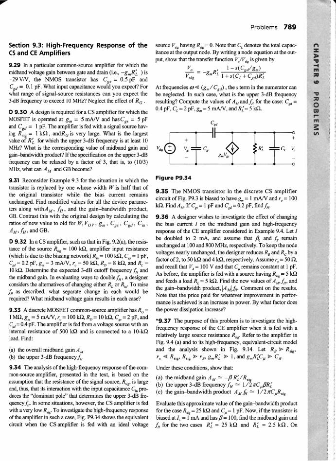
Problems 789
source v';g having R,;g = O. Note that CL denotes the total capacitance at the output node. By writing a node equation at the output, show that the transfer function V/v';g is given by
Vo ,1-s(Cg/gm) - = -g RL --.....,.-"""""-"-::-'-"'-:--:-VSlg m l+s(CL+Cgd)R~
At frequencies OJ~ (gmICgd), the s term in the numerator can be neglected. In such case, what is the upper 3-dB frequency "V
::aresulting? Compute the values of AM and IH for the case: Cgd = o0.4 pF, CL =2 pF,gm = 5 mAN, andR{= 5 ill. t:a rm s: 11\
R~
Figure P9.34
9.35 The NMOS transistor in the discrete CS amplifier circuit of Fig. P9.3 is biased to have gm = I mAN and ro = 100 ill. Find AM' IfCg, = I pF and Cgd =0.2 pF, find/H•
9.36 A designer wishes to investigate the effect of changing the bias current I on the midband gain and high-frequency response of the CE amplifier considered in Example 9.4. Let I be doubled to 2 rnA, and assume that Po and IT remain unchanged at 100 and 800 MHz, respectively. To keep the node voltages nearly unchanged, the designer reduces R8 and Re by a factor of2, to 50 ill and 4 ill, respectively. Assume rx = 50 Q, and recall that VA = 100 V and that C /1 remains constant at 1 pF. As before, the amplifier is fed with a source having R,jg = 5 ill and feeds a load RL = 5 ill. Find the new values ofAwIH' and the gain-bandwidth product, IA M/ fH. Comment on the results. Note that the price paid for whatever improvement in performance is achieved is an increase in power. By what factor does the power dissipation increase?
*9.37 The purpose ofthis problem is to investigate the highfrequency response of the CE amplifier when it is fed with a relatively large source resistance R~g. Refer to the amplifier in Fig. 9.4 (a) and to its high-frequency, equivalent-circuit model and the analysis shown in Fig. 9.14. Let R8:P Rsig ,
rx ~ Rsig, Rsig :P r ", gmRL :P 1, and gmRLCp :P C".
Under these conditions, show that:
(a) the midband gain AM = -/3 RZI Rsjg
(b) the upper 3-dB frequency fH = 112rcCp/3RL (c) the gain-bandwidth product AM.fH = 112 rcCpRsig
Evaluate this approximate value ofthe gain-bandwidth product for the case R,jg = 25 ill and C/1 = I pF. Now, ifthe transistor is biased at Ie = 1 rnA and has /3 =100, fmd the midband gain and IH for the two cases R{ = 25 kQ and R~ = 2.5 kQ. On

',~
l's
V\
:E w ....I en o a:: Q.
eft
l1li: III toA. ca: ::c u
194 Chapter 9 Frequency Response
G D
S
(a)
,o. 0 Vo
o--t + Vi
(b)
Figure P9.70
(c) For L = 0.5 /-lm, W2 = 25 /-lm,fr = 12 GHz, and floCox = 200 /-lAN2, design the circuit to obtain a gain of 3 VN per stage. Bias the MOSFETs at Vov = 0.3 V. Specify the required values of WI and 1. What is the 3-dB frequency achieved?
9.71 Consider an active-loaded common-emitter amplifier. Let the amplifier be fed with an ideal voltage source v" and neglect the effect of rx ' Assume that the bias current source has a very high resistance and that there is a capacitance CL present between the output node and ground. This capacitance represents the sum of the input capacitance of the subsequent stage and the inevitable parasitic capacitance between collector and ground. Show that the voltage gain is given by
Vo 1 -s(Cplgm) V, = -gmro l +s(CL + C1Jro
If the transistor is biased at Ie =200 /-lA and VA =100 V, CIl = 0.2 pF, and CL = 1 pF, find the dc gain, the 3-dB frequency, the frequency of the zero, and the frequency at which the gain reduces to unity. Sketch a Bode plot for the gain magnitude.
9.72 A common-source amplifier fed with a low-resistance signal source and operating with g m = 2 mAN has a unitygain frequency of 2 GHz. What additional capacitance must be connected to the drain node to reduce J; to 1 GHz?
9.73 Consider a CS amplifier loaded in a current source with an output resistance equal to roof the amplifying transistor. The amplifier is fed from a signal source with R sig = rol2. The transistor is biased to operate at gm = 2 mAN and ro = 20 kQ; Cgs = Cgd = 0.1 pF. Use the Miller approximation to determine an estimate of iH .Repeat for the following two cases: (i) the bias current I in the entire system is reduced by a factor of 4, and (ii) the bias current I in the entire system is increased by a factor of4. Remember that both Rsig and RL will change as r 0 changes.
9.74 Use the method ofopen-circuit time constants to find IH for a CS amplifier for which gm = 1.5 rnNV, Cgs = Cgd = 0.2 pF, ro = 20 kQ, RL = 12 kQ, and Rsig = 100 kQ for the following cases: (a) CL = 0, (b) CL = 10 pF, and (c) CL = 50 pF. Compare with the value of iH obtained using the Miller approximation.
Section 9.6: High-Frequency Response of the Common-Gate and Cascode Amplifiers
9.75 A CG amplifier is specified to have Cgs = 2 pF, Cgd = 0.1 pF, CL = 2pF, gm= 4rnAN, Rsig= 1 kQ, and R~ = 20 kQ. Neglecting the effects of ro , find the low-frequency gain V/Vsig, the frequencies of the poles};,1 andfn, and hence an estimate ofthe 3-dB frequency fH'
*9.76 Sketch the high-frequency equivalent circuit of a CB amplifier fed from a signal generator characterized by Vsig and Rsig and feeding a load resistance RL in parallel with a capaci
tance CL'
(a) Show that for ro = 00 the circuit can be separated into two parts: an input part that produces a pole at
1 iPI = -- II27rCjRsig re)
and an output part that forms a pole at
IP2 = 2n(CIl + CL)RL
Note that these are the bipolar counterparts of the MOS expressions in Eqs. (9.109) and (9.11 0). (b) Evaluate iPI and IP2 and hence obtain an estimate for fH for the case C" = 14 pF, CIl = 2 pF, CL = 1 pF, Ie = 1 rnA, R sig = 1 kn, and RL = 10 kn. Also, findfr of the transistor.
*9.77 Consider a CG amplifier loaded in a resistance RL = r 0 and fed with a signal source having a resistance Rsig = r/2. Also let CL = Cgs . Use the method of opencircuit time constants to show that for gm r 0 ~ I , the upper 3dB frequency is related to the MOSFET iT by the approximate expression
...
9.78 For the CG amplifier in Example 9.12, how much additional capacitance should be connected between the output node and ground to reduce III to 300 MHz?
9.79 Find the dc gain and the 3-dB frequency of aMOS cascode amplifier operated at gm = 1 mAiV and ro = 50 kn . The MOSFETs have Cgs = 30 tF, Cgd = 10 tF, and Cdb = 10 tF. The amplifier is fed from a signal source with Rsig = 100 kn and is connected to a load resistance of 2 MQ. There is also a load capacitance CL of 40 tF.
*9.80 (a) Consider a CS amplifier having Cgd = 0.2 pF, Rsig = RL = 20 kQ, gm = 4 mAN, Cgs = 2 pF, CL
(inclucling Cdh ) =I pF, Cdb = 0.2 pF, and ro = 20 kn. Find the low-frequency gain A,11' and estimate fH using open-circuit time constants. Hence determine the gain-bandwidth product. (b) Ifa CG stage is cascaded with the CS transistorin (a) to create a cascode amplifier, determine the new values of AM'flf' and gain-bandwidth product. Assume RL remains unchanged.
o 9.81 It is required to design a cascode amplifier to provide a dc gain of74 dB when driven with a low-resistance generator and utilizing NMOS transistors for which fA = 10 V, Jineox = 200 JlAN,
2 WIL = 50, Cgd = 0.1 pF, and
CL =1 pF. Assuming that RL = Ro, determine the overdrive voltage and the drain current at which the MOSFETs should be operated. Find the unity-gain frequency and the 3-dB frequency. Ifthe cascode transistor is removed and RL remains unchanged, what will the dc gain become?
9.82 Consider a bipolar cascode amplifier biased at a current of 1 rnA. The transistors used have j3 = 100, ro = 100 kn, Cl!= 14 pF, Cf.i = 2 pF, Ccs = 0, and rx = 50 n. The amplifier is fed with a signal source having Rsig = 4 kQ. The load resistance RL = 2.4 kn. Find the low-frequency gain AM' and estimate the value ofthe 3-dB frequency'~.
*9.83 In this problem we consider the frequency response of the bipolar cascode amplifier in the case that ro can be neglected.
(a) Refer to the circuit in Fig. 9.31, and note that the total resistance between the collector of QI and ground will be equal to r,2' which is usually very small. It follows that the pole introduced at this node will typically be at a very high frequency and thus will have negligible effect onfN" It also follows that at the frequencies of interest the gain from the base to the collector of QI will be -gmlre2 = -I. Use this to find the capacitance at the input of QI and hence show that the pole introduced at the input node will have a frequency
Problems 795
Then show that the pole introduced at the output node will have a frequency
If1'2 = -----...:---
2JrRL(CL + Ccs2 + Cf.i2)
(b) Evaluatefpl andfn, and use the sum-of-the-squares formula to estimate fH for the amplifier with I = 1 mA, C,,= 5 pF, Cf.i = 5 pF, Ccs = CL = 0, j3 =100, and rx = 0 in the following two cases:
(i) R sig = 1 kQ
(ii) Rsig = 10 kn
9.84 A BIT cascode amplifier uses transistors for which p= 100, VA = 100 V,fT= 1 GHz,and C,u = 0.1 pF.It operates at a bias current of 0.1 mA between a source with R sig = rJr and a load RL = pro' Let CL = Ccs = 0 and find the overall voltage gain at dc, Ill, and It .
Section 9.7: High-Frequency Response of the Source and Emitter Followers
9.85 A source follower has gm =5 mAiV, ro = 20 kn, Rsig = 20 kn, RL = 2 kn, Cgs = 2 pF, Cgd = 0.1 pF, and CL = 1 pF. Find AM' Ro'/z' andfH' Also, find the percentage contribution of each of the three capacitances to the time-constant TN"
9.86 Using the expression for the source follower III in Eq. (9.129) show that for situations in which R sig is large and RL is small,
III = ------..:..----Cgs2JrRSig[Cgd + , ]
1 + gmRL
Find III for the case Rsig= 100 kn, RL = 1 kn, ro= 20 kn, gm= 5 mAJV, Cgd = 10 iF, and Cgs= 30 iF.
9.87 Refer to Fig. 9.32(b). In situations in which Rsig is large, the high-frequency response of the source follower is determined by the low-pass circuit fonned by R sig and the input capacitance. An estimate of Cin can be obtained by using the Miller approximation to replace Cgs with an input capacitance Ceq = Cgs(1- K) where K is the gain from gate to source. Using the low-frequency value of K = gm R~ /(1 + gmR~) find Ceq and hence Cin and an estimate of Ill' Is this estimate higher or lower than that obtained by the method of open-circuit time constants?
9.88 For an emitter follower biased at Ie = 1rnA and having Rsig = RL = 1 kn, and using a transistor specified to have IT = 2 GHz, Cf.i = 0.1 pF, rx = 100 n, j3 = 100, and ~ = 20 V, evaluate the low-frequency gain AM and the 3-dB
frequency fH'